

Page 1
Geyserville-Enabled DC-DC
a
Converter Controller for Mobile CPUs
FEATURES
Meets Intel Mobile Voltage Positioning Requirements
Lowest Processor Dissipation for Longest Battery Life
Best Transient Containment
Minimum Number of Output Capacitors
System Power Management Compliant
Fast, Smooth, Output Transition During VID Code
Change
Programmable Current Limit
Power-Good
Integrated LDO Controllers for Clock and I/O Supplies
Programmable UVLO
Soft Start with Restart Lock-In
APPLICATIONS
Geyserville-Enabled Core DC-DC Converters
Fixed Voltage Mobile CPU Core DC-DC Converters
Notebook/Laptop Power Supplies
Programmable Output Power Supplies
GENERAL DESCRIPTION
The ADP3421 is a hysteretic dc-dc buck converter controller
with two auxiliary linear regulator controllers. The ADP3421
provides a total power conversion control solution for a microprocessor by delivering the core, I/O, and clock voltages. The
optimized low-voltage design is powered from the 3.3 V system
supply and draws only 10 µA maximum in shutdown. The main
output voltage is set by a 5-bit VID code. To accommodate the
transition time required by the newest processors for on-thefly VID changes, the ADP3421 features high-speed operation
to allow a minimized inductor size that results in the fastest change
of current to the output. To further allow for the minimum
number of output capacitors to be used, the ADP3421 features
active voltage positioning that can be optimally compensated
to ensure a superior load transient response. The main output
signal interfaces with the ADP3410 dual MOSFET driver,
which is optimized for high speed and high efficiency for driving
both the upper and lower (synchronous) MOSFETs of the
buck converter.
DACOUT
VID4
VID3
VID2
VID1
VID0
LTO
LTB
LTI
CLKDRV
CLKFB
IODRV
IOFB
UVLO
VCC
GND
SD
ADP3421
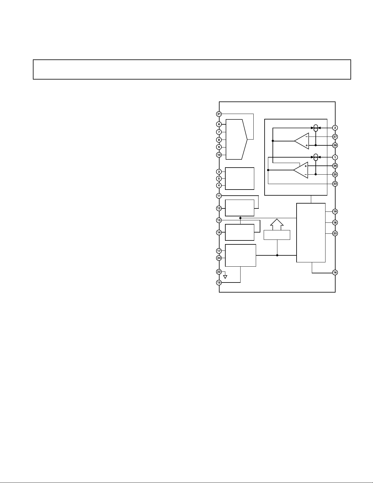
FUNCTIONAL BLOCK DIAGRAM
ADP3421
VID DAC
CURRENT
LIMIT
COMPARATOR
EN
LEVEL
TRANSLATOR
CLOCK LDO
CONTROLLER
I/O LDO
CONTROLLER
VIN/VCC
MONITOR AND
UVLO BIAS
REFERENCE
CONTROLLER
BIAS AND
REFERENCE
BIAS EN
CORE
COMPARATOR
CORE CONTROLLER
SOFT START
TIMER
AND
POWER GOOD
GENERATOR
CLSET
CS+
CS–
VHYS
REG
RAMP
OUT
SSC
SSL
CORE
PWRGD
REV. 0
Information furnished by Analog Devices is believed to be accurate and
reliable. However, no responsibility is assumed by Analog Devices for its
use, nor for any infringements of patents or other rights of third parties
which may result from its use. No license is granted by implication or
otherwise under any patent or patent rights of Analog Devices.
One Technology Way, P.O. Box 9106, Norwood, MA 02062-9106, U.S.A.
Tel: 781/329-4700 World Wide Web Site: http://www.analog.com
Fax: 781/326-8703 © Analog Devices, Inc., 1999
Page 2

ADP3421–SPECIFICATIONS
(0ⴗC ≤ TA ≤ 100ⴗC, VCC = 3.3 V, V
1
C
= 10 pF, C
OUT
= 1.8 nF, C
SSC
= VCC, V
SD
= 1.3 nF, C
SSL
= 2.0 V, V
ULVO
= 1.5 nF, unless otherwise noted)
LTB
CORE
= V
DAC
, R
OUT
= 100 k⍀,
Parameter Symbol Conditions Min Typ Max Unit
SUPPLY-UVLO-POWER-GOOD
Supply Current I
VCC UVLO Threshold I
VCC UVLO Hysteresis V
Battery UVLO Threshold V
Battery UVLO Hysteresis I
Shutdown Input Threshold V
Core Power Good Threshold V
PWRGD Output Voltage V
CC(ON)
I
CC(UVLO)
V
CCH
CCH
V
CCL
CCHYS
UVLOTH
UVLO
SDTH
COREH(UP)
V
COREH(DN)
V
COREL(UP)
V
COREL(DN)
PWRGD
V
= 0.2 V 350 µA
UVLO
V
= 0 V, 3.0 V ≤ VCC ≤ 3.6 V 10 µA
SD
2.7 V
20 mV
1.175 1.225 1.275 V
V
= 1.275 V –0.3 +0.3 µA
UVLO
= 1.175 V 0.6 1.0 1.4 µA
V
UVLO
3.0 V < VCC < 5.0 V 0.8 0.7 × VCC V
1
2
1
2
3
0.925 V < V
V
= V
CORE
= 0.8 V
V
CORE
V
= 0.2 V 0 0.4 V
UVLO
< 2.000 V 1.10 × V
DAC
DAC
DAC
1.08 × V
0.90 × V
0.88 × V
0.95 × VCC VCC V
0 0.8 V
715 mA
2.9 V
DAC
DAC
DAC
DAC
1.12 × V
1.10 × V
0.92 × V
0.90 × V
DAC
DAC
DAC
DAC
V
V
V
V
CORE CONVERTER SOFT-START TIMER
Timing Charge Current I
Discharge Current I
Enable Threshold V
Termination Threshold V
SSC(UP)
SSC(DN)
SSCEN
SSCTH
4
V
= 0 V –0.6 –1.0 –1.4 µA
SSC
V
= 1.7 V, V
SSC
= 1.1 V 0.3 1.0 mA
UVLO
150 400 mV
1.53 1.70 1.87 V
VID DAC
VID Input Threshold V
VID Input Pull-up Current I
VID0..4
Nominal Output Voltage V
Output Voltage Accuracy ∆V
Output Voltage Settling Time t
DACS
VID0..4
DAC
DAC/VDAC
5
See VID Code Table I 0.925 2.000 V
0.8 0.7 × VCC V
10 40 µA
–0.85 0.85 %
35 µs
CORE COMPARATOR
Input Offset Voltage V
Input Bias Current I
Hysteresis Current I
Hysteresis Setting Reference Voltage V
Output Voltage V
Propagation Delay Time
Rise and Fall Time
6
6
COREOS
REG
RAMP
VHYS
OUTH
V
OUTL
t
COREPD
8
t
,710ns
CORER
8
t
COREF
V
= 1.3 V –3 +3 mV
REG
V
= V
REG
V
CORE
= 1.30 V, V
V
CS–
= 1.28 V
V
REG
R
VHYS
R
VHYS
R
VHYS
= 1.32 V
V
REG
R
VHYS
R
VHYS
R
VHYS
= V
= 1.3 V –2 +2 µA
RAMP
= 1.3 V
RAMP
= 1.28 V
CS+
Open –2 +2 µA
= 170 kΩ –7 –10 –13 µA
= 17 kΩ –82 –97 –113 µA
Open –2 +2 µA
= 170 kΩ 71013µA
= 17 kΩ 82 97 113 µA
1.53 1.70 1.87 V
VCC = 3.0 V 2.5 3.0 V
VCC = 3.6 V 0 0.4 V
7
T
= 25°C20ns
A
0°C ≤ T
≤ 100°C30ns
A
REV. 0–2–
Page 3

ADP3421
Parameter Symbol Conditions Min Typ Max Unit
CURRENT LIMIT COMPARATOR
Input Offset Voltage V
Input Bias Current I
Hysteresis Current I
Hysteresis Setting Reference Voltage V
Propagation Delay Time
6
CLOS
CL+
CL–
VHYS
t
CLPD
7
LINEAR REGULATOR SOFT-START TIMER
Charge Current I
Discharge Current I
Enable Threshold V
Termination Threshold V
SSC(UP)
SSC(DN)
SSCEN
SSCTH
4
2.5 V CLK LDO CONTROLLER
Feedback Bias Current I
Output Drive Current I
DC Transconductance G
CLKFB
CLKDRV
CLK
1.5 V I/O LDO CONTROLLER
Feedback Bias Current I
Output Drive Current I
DC Transconductance G
IOFB
IODRV
IO
LEVEL TRANSLATOR
Input Clamping Threshold V
Output Voltage V
Propagation Delay Time
NOTES
1
V
ramps up monotonically.
CORE
2
V
ramps down monotonically.
CORE
3
During latency time of VID code change, the Power-Good output signal should not be considered valid.
4
Internal bias and soft start are not enabled unless the soft-start pin voltage first drops below the enable threshold.
5
Measured from 50% of VID code transient amplitude to the point where V
6
Guaranteed by characterization.
7
40 mV p-p amplitude impulse with 20 mV overdrive. Measure from the input threshold intercept point to 50% of the output voltage swing.
8
Measured between the 30% and 70% points of the output voltage swing.
9
The LTO output tied to V
Specifications subject to change without notice.
6
= 2.5 V rail through an R
CCLT
LTIH
LTOH
V
LTOL
t
LTPD
LTO
V
= 1.3 V –6 +6 mV
CS–
V
= 1.3 V –5 +5 µA
CS+
V
CORE
= 1.28 V, V
V
REG
= 1.28 V
V
CS+
R
IHYS
R
IHYS
R
IHYS
= 1.32 V
V
CS+
R
IHYS
R
IHYS
R
IHYS
= V
= 1.3 V
RAMP
= 1.3 V
CS–
Open –5 µA
= 170 kΩ –22 –30 –38 µA
= 17 kΩ –265 –300 –335 µA
Open –5 µA
= 170 kΩ –13 –20 –27 µA
= 17 kΩ –175 –200 –225 µA
1.53 1.70 1.87 V
T
= 25°C3060ns
A
0°C ≤ TA ≤ 100°C 50 100 ns
V
= 0 V –0.6 –1.0 –1.4 µA
SSC
V
= 1.7 V, V
SSC
= 1.1 V 0.3 1.0 mA
UVLO
150 400 mV
1.53 1.70 1.87 V
V
= 2.5 V 12.5 25 µA
CLKFB
V
V
∆I
V
V
V
∆I
I
I
V
= 2.55 V 1 µA
CLKDRV
= 2.45 V 3 20 mA
CLKDRV
= 1 mA 500 mA/V
CLKDRV
= 1.5 V 7.5 15 µA
IOFB
= 1.53 V 1 µA
IODRV
= 1.47 V 10 60 mA
IODRV
= 1 mA 650 mA/V
CLKDRV
= –10 µA 0.95 1.5 V
LTI
= –10 µA
LTI
= 0.175 V
LTI
9
9
0.9 × V
CCLT
V
375 mV
10 ns
settles within ±1% of its steady state value.
DAC
= 150 Ω pull-up resistor.
CCLT
V
REV. 0 –3–
Page 4
ADP3421
WARNING!
ESD SENSITIVE DEVICE
ABSOLUTE MAXIMUM RATINGS*
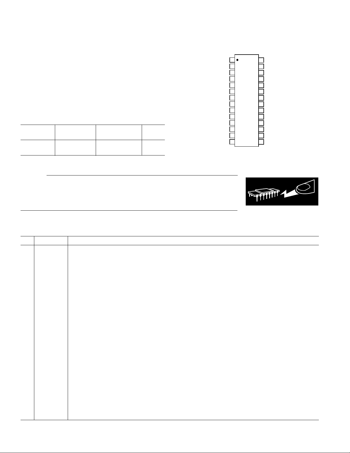
PIN CONFIGURATION
Input Supply Voltage (VCC) . . . . . . . . . . . . . . –0.3 V to +7 V
UVLO Input Voltage . . . . . . . . . . . . . . . . . . . . –0.3 V to +7 V
All Other Inputs/Outputs . . . . . . . . . . . . . . . . . . VCC + 0.3 V
Operating Ambient Temperature Range . . . . . . 0°C to 100°C
Junction Temperature Range . . . . . . . . . . . . . . . 0°C to 150°C
. . . . . . . . . . . . . . . . . . . . . . . . . . . . . . . . . . . . . . . . 98°C/W
θ
JA
Storage Temperature Range . . . . . . . . . . . . –65°C to +150°C
Lead Temperature (Soldering, 10 sec.) . . . . . . . . . . . . . 300°C
*This is a stress rating only; operation beyond these limits can cause the device to
be permanently damaged.
ORDERING GUIDE
Temperature Package Package
Model Range Description Option
ADP3421JRU 0°C to 100°C Thin Shrink Small RU-28
CLKDRV
VHYS
CLSET
LTO
LTI
LTB
VID4
VID3
VID2
VID1
VID0
CLKFB
IODRV
IOFB
1
2
3
4
5
6
ADP3421
7
TOP VIEW
(Not to Scale)
8
9
10
11
12
13
14
Outline (TSSOP)
CAUTION
ESD (electrostatic discharge) sensitive device. Electrostatic charges as high as 4000 V readily
accumulate on the human body and test equipment and can discharge without detection.
Although the ADP3421 features proprietary ESD protection circuitry, permanent damage may
occur on devices subjected to high-energy electrostatic discharges. Therefore, proper ESD
precautions are recommended to avoid performance degradation or loss of functionality.
28
27
26
25
24
23
22
21
20
19
18
17
16
15
CS–
CS+
REG
RAMP
VCC
OUT
GND
DACOUT
CORE
SSC
SSL
UVLO
PWRGD
SD
PIN FUNCTION DESCRIPTIONS
Pin Mnemonic Function
1 VHYS Core Comparator Hysteresis Setting. The voltage at this pin is held at a 1.7 V reference level. A resistor to
ground programs at a 1:1 ratio the current that is alternately switched into and out of the RAMP pin.
2 CLSET Current Limit Setting. The voltage at this pin is held at a 1.7 V reference level. A resistor to ground programs
a current that is gained up by 3:1 flowing out of the CS– pin, assuming the current limit comparator is not
triggered.
3 LTO Level Translator Output. This pin must be tied through a pull-up resistor to the voltage level desired for the
output high level. That voltage cannot be less than 1.5 V.
4 LTI Level Translator Input. This pin should be driven from an open drain/collector signal. The pull-up current is
provided by the pull-up resistor on the LTO pin. However, the pull-up current will be terminated when the
LTI pin reaches 1.5 V.
5 LTB Level Translator Bypass. For operation of the level translator with high-speed signals, this pin should be by-
passed to ground with a large value capacitor.
6 VID4 VID Input. Most significant bit.
7 VID3 VID Input.
8 VID2 VID Input.
9 VID1 VID Input.
10 VID0 VID Input. Least significant bit.
11 CLKDRV 2.5 V Linear Regulator Driver Output. This pin sinks current from the base of a PNP transistor as needed to
keep the CLKFB node regulated at 2.5 V.
12 CLKFB 2.5 V Linear Regulator Output Feedback. This pin is connected to the collector of a PNP transistor whose
base is driven by the CLKDRV pin.
13 IODRV 1.5 V Linear Regulator Driver Output. This pin sinks current from the base of a PNP transistor as needed to
keep the IOFB node regulated at 1.5 V.
14 IOFB 1.5 V Linear Regulator Output Feedback. This pin is connected to the collector of a PNP transistor whose
base is driven by the IODRV pin.
–4–
REV. 0
Page 5

ADP3421
Pin Mnemonic Function
15 SD Shutdown Input. When this pin is pulled low, the IC shuts down and all regulation functions will be disabled.
16 PWRGD Power-Good Output. This signal will go high only when the SD pin is high to allow IC operation, the UVLO
and VCC pins are above their respective start-up thresholds, the SSC and SSL pins are above a voltage where
soft start is completed, and the voltage at the CORE pin is within the specified limits of the programmed VID
voltage. By choosing the soft-start capacitor for the core larger than that for the linear regulators, at start-up
the core and linear outputs should all be in regulation before PWRGD is asserted.
17 UVLO Undervoltage Lockout Input. This pin monitors the input voltage through a resistor divider. When the pin
voltage is below a specified threshold, the IC enters into UVLO mode regardless of the status of SD. When
in UVLO mode, a current source is switched on at this pin, which sinks current from the external resistor
divider. The generated UVLO hysteresis is equal to the current sink value times the upper divider resistor.
18 SSL Linear Regulator Soft Start. During power-up, an external soft-start capacitor is charged by a current source
to control the ramp-up rates of the linear regulators.
19 SSC Core Voltage Soft Start. During power-up, an external soft-start capacitor is charged by a current source to
control the ramp-up rate of the core voltage.
20 CORE Core Converter Voltage Monitor. This pin is used to monitor the core voltage for power-good verification.
21 DACOUT VID-programmed Digital-to-Analog Converter Output. This voltage is the reference voltage for output
voltage regulation.
22 GND Ground.
23 OUT Logic-Level Drive Signal Output of Core Controller. This pin provides the drive command signal to the IN
pin of the ADP3410 driver. This pin is not capable of directly driving a power MOSFET.
24 VCC Power Supply.
25 RAMP Current Ramp Input. This pin provides the negative feedback for the core output voltage. The switched sink/
source current from this pin, which is set up at the VHYS pin, works against the terminating resistance at this
pin to set the hysteresis for the hysteretic control.
26 REG Regulation Voltage Summing Input. In the recommended configuration, the DACOUT voltage and the core
voltage are summed at this pin to establish regulation with output voltage positioning.
27 CS+ Current Limit Positive Sense. This pin senses the positive node of the current sense resistor.
28 CS– Current Limit Negative Sense. This pin connects through a resistor to the negative node of the current sense
resistor. A current flows out of the pin, as programmed at the CLSET pin. When this pin is more negative
than the CS+ pin, the current limit comparator is triggered and the current flowing out of the pin is reduced
to two-thirds of its previous value, producing a current limit hysteresis.
REV. 0
–5–
Page 6

ADP3421–Typical Performance Characteristics
LOAD CURRENT – A
CLK LDO REGULATOR OUTPUT VOLTAGE – V
2.45
100m 1m 0.01
2.50
2.55
0.1 1
b
EXT
= 100
2.40
2.60
100m
NORMAL OPERATING MODE
10m
1m
UVLO MODE
100m
SUPPLY CURRENT – A
SHUTDOWN MODE
10m
1m
0
20 10040 60 80
TEMPERATURE – 8C
Figure 1. Supply Current vs.
Temperature
2.010
2.000
1.990
0.9375
DAC OUTPUT – V
0.925
0.9125
+0.85%
–0.85%
+0.85%
–0.85%
0
20 10040 60 80
AMBIENT TEMPERATURE – 8C
FULL SCALE
ZERO SCALE
Figure 4. DAC Output Voltage vs.
Temperature
HIGH
POWER-GOOD
LOW
–0.15 –0.1 0.1–0.05 0 0.05
RELATIVE CORE VOLTAGE – DV
CORE
/ V
0.15
CORE
Figure 2. Power-Good vs. Relative
Core Voltage Variation
100
OUT = HIGH, RHYS = 17kV
OUT = HIGH, RHYS = 170kV
0
OUT = LOW, RHYS = 170kV
HYSTERESIS CURRENT – mA
–100
OUT = LOW, RHYS = 17kV
0
20 10040 60 80
AMBIENT TEMPERATURE – 8C
Figure 5. Core Hysteresis Current vs.
Temperature
1000
100
10
1
SOFT-START TIME – ms
0.1
0.1 100110
CORE FULL SCALE
CORE ZERO SCALE
AND LDOS
TIMING CAPACITANCE – nF
Figure 3. Soft-Start Time vs. Timing
Capacitance
0
–100
–200
–300
CURRENT LIMIT THRESHOLD CURRENT – mA
OUT = LOW, R
OUT = LOW, R
OUT = HIGH, R
0
20 10040 60 80
AMBIENT TEMPERATURE – 8C
= 170kV
CLSET
OUT = HIGH, R
= 17kV
CLSET
= 17kV
CLSET
CLSET
= 170kV
Figure 6. Current Limit Threshold
Current vs. Temperature
40
30
V
= 1.47V
IOFB
20
10
OUTPUT DRIVE CURRENT – mA
V
= 2.45V
CLKFB
0
0
20 10040 60 80
AMBIENT TEMPERATURE – 8C
IO LDO
CLK LDO
Figure 7. LDO Drive Current vs.
Temperature
1.55
b
1.52
1.50
1.48
IO LDO REGULATOR OUTPUT VOLTAGE – V
1.45
100m 1m 0.01
LOAD CURRENT – A
0.1 1 10
EXT
= 100
Figure 8. IO LDO DC Load Regulation
–6–
Figure 9. CLK LDO DC Load
Regulation
REV. 0
Page 7

ADP3421
THEORY OF OPERATION
Supply Voltages
The ADP3421 is optimized for use with, and specified at a
3.3 V supply, but can operate at up to 6 V at the expense of
increased quiescent current and minor tolerance degradation.
The ADP3410 MOSFET driver can accommodate up to 30 V
for driving the upper power MOSFET to 5 V above a 25 V rail.
Undervoltage Lockout
The undervoltage lockout (UVLO) circuit comprises the low
and low VCC detection comparators. UVLO for VIN pro-
V
IN
vides a system UVLO that monitors the battery voltage and
allows the converter operation to be disabled if the battery falls
below a preset threshold. A resistor divider to the UVLO pin
sets the UVLO-off level for the system comparing to a specified
reference. When V
goes low enough to activate UVLO, this
IN
triggers a specified current sink into the pin to be switched on.
This raises the UVLO-on threshold above the UVLO-off
threshold by the current sink values times the upper resistor of
the divider. So the resistor divider ratio at the UVLO pin is
used to set the UVLO threshold and the hysteresis.
Hysteresis for the system UVLO is recommended to prevent
oscillation due to nonzero battery impedance. If UVLO is triggered during a condition where the battery is loaded by the
converter operation, the converter will turn off and the battery
voltage will then rise to a slightly higher level. A good design
will ensure that the hysteresis is sufficient to prevent the converter
from turning on again.
UVLO for VCC provides an internally specified UVLO threshold for the ADP3421 to ensure that it only operates when the
applied VCC is sufficient to ensure that it can operate properly.
Activation of either UVLO circuit disables the reference and
bias circuits in the IC except for that which is needed for UVLO
detection.
Power Good
If the IC is enabled and is not in the UVLO mode and has fin-
ished its soft-start period, and if the core voltage is within ±10%
of the VID programmed value, then a high-level signal appears
at the PWRGD pin.
Power Good During VID Change
When a VID change occurs, the DAC output responds faster than
the output voltage, which is slew-rate limited by the output
filter. In this case, PWRGD may momentarily go low. To avoid
system interruption, the PC power management system should
not respond to this glitch. The PWRGD signal corresponds to
V_GATE as specified in Intel’s Geyserville Voltage Regulator
specification. The glitch can be masked from the system by
using the appropriate system programming settings or by using
a functionally-equivalent OR gate, which provides a blanking
signal for the specified latency period in which the core voltage
is allowed to settle at its new value. Because of the minimal output capacitor requirement, the response time of the core voltage
is well within the specified latency period and, when the power
converter is properly compensated, it does not exhibit any
overshoot.
VID Programmed DAC Reference
This 5-bit digital-to-analog converter (DAC) serves as the
programmable reference source of the dc-dc converter. Programming is accomplished by CMOS logic level VID code
applied to the DAC input. The VID code corresponds to that
recommended in guidelines for the mobile Pentium
®
-III published
by Intel. (See Table I.)
Table I. VID Code
VID4 VID3 VID2 VID1 VID0 VOUT
000002.000
000011.950
000101.900
000111.850
001001.800
001011.750
001101.700
001111.650
010001.600
010011.550
010101.500
010111.450
011001.400
011011.350
011101.300
01111Off*
100001.275
100011.250
100101.225
100111.200
101001.175
101011.150
101101.125
101111.100
110001.075
110011.050
110101.025
110111.00
111000.975
111010.950
111100.925
11111Off*
*No CPU-shutdown.
Core Comparator
The core comparator is an ultrafast hysteretic comparator with
a typical propagation delay to the OUT pin of 15 ns at a 20 mV
overdrive.
This comparator is used with a switched hysteresis current for
controlling the main feedback loop, as described in the Main
Feedback Loop Operation section. This comparator has no
relation to the CORE pin, which is used only for core voltage
monitoring for the PWRGD function.
Current Limit Comparator
The current limit comparator monitors the voltage across the
current-sense resistor R
and it overrides the core comparator
CS
and forces the OUT pin to low when the current exceeds the
peak current limit threshold. The current control is hysteretic,
with a valley current threshold equal to two-thirds of the peak
current limit threshold. When the sensed current signal falls to
two-thirds of the peak threshold, the OUT pin is allowed to go
high again, and the control of the main loop reverts back to the
core comparator.
Pentium is a registered trademark of Intel Corp.
REV. 0
–7–
Page 8

ADP3421
A resistor (R
) connected between the CLSET and ground
CLS
sets a current that is internally multiplied by a factor of three
and flows out of the CS– pin. The resistor R
connected in
CL
series with the CS– pin to the negative current sense point (i.e.,
the output voltage) sets the voltage that must be developed
across R
to trip the current limit comparator. Once it is tripped,
CS
the CS– current is scaled down by two-thirds, so the inductor
current must ramp down accordingly to reset the comparator.
Core Converter Soft-Start Timer
The soft-start function limits the ramp-up time of the core voltage in order to reduce the initial inrush current on the core
input voltage (battery) rail. The soft-start circuit consists of an
internal current source, an external soft-start timing capacitor,
an internal switch across the capacitor, and a comparator
monitoring the capacitor voltage.
The soft-start capacitor is held discharged when either the SD
signal is low or the device is in UVLO mode. As soon as SD is
set to high, and VCC and V
rise above their respective UVLO
IN
thresholds, the short across the external timing capacitor is
removed, and the internal soft-start current source begins to
charge the timing capacitor. During the charge of the soft-start
capacitor, the Power-Good signal is set to low. When the timing
capacitor voltage reaches an internally set soft-start termination
threshold, the core monitor window comparator output is
enabled, allowing the Power-Good status to be determined. If
the core voltage has already settled within the specified limits
the Power-Good signal goes high, otherwise it stays low. The
soft-start capacitor remains charged until either SD goes low,
or VCC or V
drop below their respective UVLO thresholds.
IN
When this occurs, an internal switch quickly discharges the
soft-start timing capacitor to prepare the IC for a new start-up
sequence.
Soft-Start Restart Lock In
In the event that a UVLO event was not long enough to allow
the soft-start capacitors to discharge (e.g., a momentary power
glitch), the UVLO event is captured by a latch. The forced discharge of the soft-start capacitors will continue until a lower
threshold is reached, at which time the converter will restart
with a fully controlled soft start.
1.5 V I/O Voltage Regulator
Two pins control an external PNP, for example, transistor as
a linear regulator for a 1.5 V output. The IODRV pin directly
drives the base of the PNP with ≥10␣ mA to support an output
current as high as the PNP’s current gain and power dissipation
capability will allow. For example, with a high gain PNP transistor
such as the Zetex ZFT788B (SOT-223), the I/O linear regulator
is capable of delivering peak currents of greater than 2.5 A. The
1.5 V output is connected to the IOFB pin to provide feedback.
2.5 V CLK LDO Voltage Regulator
Two pins control an external PNP transistor as a linear regulator
for a 2.5 V output. The CLKDRV pin, for example, directly
drives the base of the PNP with ≥3 mA to support an output
current as high as the PNP’s current gain and power dissipation
capability will allow. For example, with a high gain PNP transistor such as the Zetex ZFT788B (SOT-223), the CLK linear
regulator is capable of delivering peak currents of greater than
1.2 A. The 2.5 V output is connected to the CLKFB pin to
provide feedback.
Linear Regulator Soft-Start Timer
The soft-start timer circuit of the linear regulators is similar to
that of the core converter, and is used to control the ramp-up
time of the linear regulator output voltages. For maximum
flexibility in controlling the start-up sequence, the soft-start
function of the linear regulators was separated from that of the
core converter.
Level Translator
The level translator converts any digital input signal to a userprogrammable voltage level. This can be used to translate an
IO-level signal (i.e., 1.5 V) into a CLK-level or VCC-level or
even 5 V-level signal. For example, the 1.5 V FERR# signal can
be converted to a 3.3 V level for the PII-X4 chipset. The output
signal is in phase with the input, and it is not necessary to have
a pull-up on the input signal. The ADP3421 provides pull-up
for the input signal to 1.5 V. The only practical restriction on
the input signal is that it must not prevent pull-up to 1.5 V. An
external pull-up resistor sets the output signal level. Throughput
time for the signal using a 150 Ω pull-up resistor is 5 ns (typ).
APPLICATION INFORMATION
Overview—Combined ADP3421 and ADP3410 Power Controller for PC Systems
The ADP3421 is a power controller that can provide a regulation solution for all three power rails of an Intel Pentium II or
III processor. Together with the ADP3410 driver IC, these ICs
form an integral part of a PC system, featuring a high-speed
(<10 ns) level translator, interface with GCL and PII-X4
or other power management signals, and a power sequenced
switched 5 V rail. For high-slew-rate microprocessors, this
minimizes the total solution cost by allowing the quantity of
output capacitors to be minimized to the limit of what the buck
converter topology and the capacitor technology can allow.
Recommended Configuration
The ADP3421 controls the regulation of the core voltage without amplifiers in a unique ripple regulator control topology. In
a proprietary optimized compensation configuration offered
by Analog Devices, Inc., the inductor ripple current is kept at a
fixed programmable value while the output voltage is regulated
with fully programmable voltage positioning parameters, which
can be tuned to optimize the design for any particular CPU
regulation specifications. By fixing the ripple current, the frequency variations associated with changes in output capacitance
and ESR for standard ripple regulators will not appear.
Accurate current sensing is needed to accomplish accurate output voltage positioning, which, in turn, is required to allow the
minimum number of output capacitors to be used to contain
transients. A current-sense resistor is used between the inductor
and the output capacitors. To allow the control to operate without amplifiers, the negative feedback signal is taken from the
inductor, or upstream, side of the current-sense resistor, and the
positive feedback signal is taken from the downstream side.
Active voltage positioning, whose advantages are described later,
has two parameters that are separately controlled. The negative
feedback signal uses a resistor divider to ground into the RAMP
pin to create the precise offset voltage needed for voltage positioning. The positive feedback signal and the DAC’s VID-controlled
reference are summed into the REG pin through resistors to set
the desired voltage positioning gain. The proprietary optimal com-
pensation is a final parameter that must be tuned to ensure that
–8–
REV. 0
Page 9

ADP3421
the voltage positioning is not bandwidth limited. This is accomplished by using the appropriately-sized capacitor in parallel
with the resistor that sums the positive feedback signal. The
optimal compensation also gives the ripple current control that
adds stability to the switching frequency.
Standard Hysteretic Control Configuration
The ADP3421 can also be used as a conventional hysteretic
ripple regulator where the output ripple voltage is directly programmed. To achieve this conventional operation, the DAC’s
output is connected directly to the REG pin and the output
voltage connects through a resistor to the RAMP pin. This resistor
sets the output ripple voltage, which will be symmetrically centered
around the DAC voltage. If the optimal DAC voltage is not
available, an offset could be summed into the RAMP pin with
another resistor, as was done with the previous configuration.
Intel Mobile Voltage Positioning Implementation
In the recommended configuration, the ADP3421 uses voltage
Intel Mobile Voltage positioning technology as an inherent part
of its architecture.
No matter how fast the response of the switches, even instantaneous, the inductor limits the response speed at the output of
the converter. This places the primary burden of transient
response containment on the output capacitors. The size and
cost of the output capacitors can be minimized by keeping the
output voltage higher at light load in anticipation of a load
increase, and lowering the output voltage at heavier loads in
anticipation of a load decrease. Voltage positioning with the
ADP3421 is active, which means the voltage positioning can be
controlled by loop gain. This increases efficiency compared to
passive voltage positioning that is sometimes used as a supplementary regulation technique with voltage-mode controllers.
Instead of sizing a series resistor to create the entire voltage drop
(often called a “droop” resistor in the passive voltage positioning
implementation), a smaller value current-sensing resistor can be
used and the loop can amplify its voltage drop to position the
voltage as desired without additional power loss.
Voltage Positioning for Power Savings
In addition to the size and cost reduction of the output capacitors,
another advantage of using voltage positioning is a reduction
in the CPU core dissipation. That dissipation is equal to the
product of the applied core voltage and the current drawn by
the CPU. The CPU current is primarily due to the capacitive
switching load of digital circuitry, and it is also proportional to
the applied voltage. The result is that the CPU power dissipation is
approximately proportional to the applied voltage squared.
P
CPU
= k × V
CPU
2
This characteristic, combined with the wide tolerance on the
core voltage specification, suggests that the maximum CPU
power dissipation can be substantially reduced by setting the
core voltage near the lower specified voltage limit. For example,
if a 1.6 V processor is operated 7% below its nominal voltage
rating, the CPU power dissipation is reduced by 13.5%. Losses
in the switches and inductor of the power converter are also
reduced due to the decrease in maximum load current.
To realize the full cost-reducing benefits of active voltage positioning, a current-sensing resistor should be used in order to
convey accurate current information to the control loop. This is
needed to accurately position the core voltage as a function of
load current, and accurate positioning of the core voltage allows
the highest reduction in output capacitors. It is common to see
passive voltage positioning implemented by sensing voltage drop
on a copper trace or across a power MOSFET. This causes poor
control of the voltage positioning—a tolerance analysis can show
the weakness of this design technique.
Although additional power is dissipated by the current-sense
resistor, the total power consumption is reduced because of the
squared reduction of current consumption by the CPU. For
example, if the CPU draws 15␣ A at 1.6␣ V, the current-sensing
resistor is 3␣ mΩ, and the supply voltage is reduced by 7%, the
core dissipation can be reduced from 24␣ W to:
24 W␣ ×␣ 0.93
2
= 20.76␣ W,
and the power dissipated in the resistor is only:
[20.76 W/(1.6 V × 0.93)]
2
× 3 mΩ = 0.58␣ W.
The total power savings from the battery is 2.65␣ W, or 11.1%.
Optimally Compensated for Voltage Positioning
Although voltage positioning helps to control the initial load
transient, high-frequency load repetition rates can cause the
voltage to exceed by double the limits within which the transients can be contained. For complete transient containment
over the bandwidth of the core’s transient activity, the solution
is an enhanced optimally compensated version of voltage
positioning.
It prevents the tendency of the core voltage to “bounce” before
settling to its final positioned value after the inductor current
has been ramped to its final value.
Main Feedback Loop Operation
In conjunction with a selected control topology, the ADP3421
regulates a drive control signal at the OUT pin using a comparator.
The two inputs are pins RAMP (–) and REG (+). A bidirectional
switched control current is used at the RAMP input to establish
hysteresis with a chosen termination resistance. Beginning in the
drive high state (OUT pin high), the control current is sinking
current into the RAMP pin, but the output current in the buck
converter is increasing and so V
RAMP
will eventually exceed V
REG
.
When this happens, the control current reverses and sources
current out of the RAMP pin to provide both hysteresis and
overdrive for the comparator. The OUT pin goes low and the
buck converter output current decreases until V
RAMP
< V
REG
,
at which time the comparator switches, the control current
reverses, and the process repeats.
How the hysteresis current is used (depending on the control
configuration) will determine which parameter is hysteretically
controlled—presumably either the inductor ripple current or the
output ripple voltage, as in the two suggested configurations, or
a weighted combination of the two or another variable could be
introduced.
Core Converter Design Procedure
There are two primary objectives considered in optimizing the
design of a power converter. The first objective is to meet the
specifications; the second objective is to do so at the lowest cost.
Analog Devices, Inc., addresses both of these objectives with the
ADP3421 and its recommended design procedure. The optimized
design yields the additional benefit of reducing the maximum
CPU power consumption by ~10% for typical CPU specifications, which has created great interest to those using the CPU.
REV. 0
–9–
Page 10

ADP3421
Microprocessors have the distinguishing characteristic of
creating extremely fast load transients from nearly zero to the
maximum load and vice versa. The advent of increasing power
management (used to interrupt the CPU processing) causes
these transients to occur with increasing frequency. Since it takes a
far longer time (typically on the order of several microseconds)
to ramp the inductor current up or down to the correct average
value after a load transient has occurred, the output capacitors
must supply or absorb the extra charge during that period of
time. This causes the output voltage to dip down or peak up.
In order to contain the output voltage within the specified limits
during load transients, with the minimum quantity of output
capacitors, the output voltage must be positioned as a function
of load, and it must be done so accurately. Therefore, currentsensing with a discrete resistor (e.g., rather than using trace
resistance) is strongly recommended, as this will allow the number
of capacitors to be reduced toward the theoretical minimum—
which is nearly half as many as required for a standard fixedregulation technique. This is the key to minimizing the cost (and
also size) of the power converter.
The voltage should be positioned (i.e., regulated) high at no
load and low at maximum load. This means that the power
supply will appear to have an initial offset and reduced load
regulation, because the output voltage will regulate higher than
nominal at no load and below nominal at maximum load. This
regulation technique positions the voltage in anticipation of a
load transient. At no load, the voltage is high, so when the load
transient strikes, the downward dip can be more easily contained
within the limits. Similarly at maximum load, the voltage is low,
so when the load transient strikes, the upward peak can be more
easily contained.
Multiple MLC capacitors will always be needed on the output
across the CPU power pins to handle the high-frequency component of the transient with minimized series inductance to and
through the bulk capacitors of the power converter’s output filter.
Although there are numerous trade-offs between size and cost of
various combinations of capacitor types for meeting a given
specification, the accurate voltage positioning provided by the
ADP3421 will allow the overall combination of capacitors to be
minimized.
A key requirement for optimizing the dynamic performance
of a power converter with accurate voltage positioning is to
apply “optimal compensation”—that is, the compensation that
creates a loop response that causes the output voltage to settle
immediately after a load transient, resulting in a “flat” transient
response. The ADP3421’s unique architecture is designed to
accommodate this ADI proprietary optimal compensation
technique in core dc-dc converters for Mobile CPUs. It is implemented by creating the proper frequency response characteristic
at the summing junction of the output voltage and the DAC
voltage, which occurs at the REG pin.
The complete design procedure is supplied in a separate application note from Analog Devices, Inc., entitled: DC-DC Power
Converter Design using the ADP3421 Controller.
PRINTED CIRCUIT BOARD LAYOUT
CONSIDERATIONS
The ADP3421 is a high-speed controller capable of providing
a response time well under 100 ns. In order to avoid having the
ADP3421 respond to noise, the first step in achieving good noise
immunity is to follow the layout considerations.
In some layouts it may be necessary to supplement the ADP3421
control design with additional components designed to minimize
noise problems. For this purpose, some additional hysteresis can
be added around the core and current limit comparators. This
takes the form of adding a small capacitor (~1 pF) from OUT to
REG (for the main loop) and OUT to CS– (for current limit
loop), and providing some resistance for the capacitive hysteresis feedback to work against. For the current limit loop, this
register is already in the basic circuit. For the main loop, this
resistor must be added between the REG pin and the standard
feedback components. This provides a quick dynamic hysteresis
with a small time constant that is chosen only long enough to
ensure that the switching noise ringing through the circuit has
decayed by the time the dynamic hysteresis is substantially lost.
The following guidelines are recommended for optimal performance of the ADP3421 and ADP3410 in a power converter.
The circuitry is considered in four parts: the power switching
circuitry, the output filter, the control circuitry, and the LDOs.
Placement Overview
1. For ideal component placement, the output filter capacitors
will divide the power switching circuitry from the control
section. As an approximate guideline, considered on a singlesided PCB, the best layout would have components aligned
in the following order: ADP3410, MOSFETs and input
capacitor, output inductor, current-sense resistor, output
capacitors, control components, and ADP3421. Note that
the ADP3421 and ADP3410 are completely separated for
an ideal layout, which is only possible with a two-chip solution. This will minimize jitter in the control caused by having
the driver and MOSFETs close to the control and give
more freedom in the layout of the power switching circuitry.
2. Whenever a power dissipating component (e.g., a power
MOSFET) is soldered to a PCB, the liberal use of vias, both
directly on the mounting pad and immediately surrounding
it, is recommended. Two important reasons for this are:
improved current rating through the vias (if it is a current
path), and improved thermal performance—especially if the
vias extend to the opposite side of the PCB where a plane
can more readily transfer heat to air.
–10–
REV. 0
Page 11

ADP3421
Power Switching Circuitry
ADP3410, MOSFETs, Input Capacitors
3. Locate the ADP3410 near the MOSFETs so the parasitic
inductance in the gate drive traces and the trace to the SW
pin is small, and so that the ground pins of the ADP3410 are
closely connected to the lower MOSFET’s source.
4. Locate at least one substantial (i.e., > ~1 µF) input bypass
MLC capacitor close to the MOSFETs so that the physical
area of the loop enclosed in the electrical path through the
bypass capacitor and around through the top and bottom
MOSFETs (drain-source) is small. This is the switching
power path loop.
5. Make provisions for thermal management of all the MOSFETs.
Heavy copper and wide traces to ground and power planes will
help to pull out the heat. Heat sinking by a metal tap soldered
in the power plane near the MOSFETs will help. Even just
small airflow can help tremendously. Paralleled MOSFETs will
help spread the heat, even if the on-resistance is higher.
6. An external “antiparallel” Schottky diode (across the bottom
MOSFET) may help efficiency a small amount (<␣ ~1␣ %); a
MOSFET with a built-in antiparallel Schottky is more effective. For an external Schottky, it should be placed next to the
bottom MOSFET or it may not be effective at all. Also, a
higher current rating (bigger device with lower voltage drop)
is more effective.
7. Both ground pins of the ADP3410 should be connected into
the same ground plane with the power switching circuitry,
and the VCC bypass capacitor should be close to the VCC
pin and connected into the same ground plane.
Output Filter
Output Inductor and Capacitors, Current-Sense Resistor
8. Locate the current-sense resistor very near to the output
capacitors.
9. PCB trace resistances from the current-sense resistor to the
output capacitors, and from the output capacitors to the
load, should be minimized, known (calculated or measured),
and compensated for as part of the design if it is significant.
(Remote sensing is not sufficient for relieving this requirement.) A square section of 1-ounce copper trace has a
resistance of ~500 mΩ. Using 2~3 squares of copper can
make a noticeable impact on a 15␣ A design.
10. Whenever high currents must be routed between PCB layers,
vias should be used liberally to create several parallel current
paths so that the resistance and inductance introduced by
these current paths is minimized and the via current rating
is not exceeded.
11. The ground connection of the output capacitors should be
close to the ground connection of the lower MOSFET and
it should be a ground plane. Current may pulsate in this
path if the power source ground is closer to the output
capacitors than the power switching circuitry, so a close
connection will minimize the voltage drop.
Control Circuitry
ADP3421, Control Components
12. If the placement overview cannot be followed, the ground
pin of the ADP3421 should be Kelvin-connected into the
ground plane near the output capacitors to avoid introducing ground noise from the power switching stage into the
control circuitry. All other control components should be
grounded on that same signal ground.
13. If critical signal lines (i.e., signals from the current-sense
resistor leading back to the ADP3421) must cross through
power circuitry, it is best if a signal ground plane can be
interposed between those signal lines and the traces of the
power circuitry. This serves as a shield to minimize noise
injection into the signals at the expense of making signal
ground a bit noisier.
14. Absolutely avoid crossing any signal lines over the switching
power path loop, as previously described.
15. Accurate voltage positioning depends on accurate current
sensing, so the control signals that differentially monitor
the voltage across the current-sense resistor should be
Kelvin-connected.
16. The RC filter used for the current-sense signal should be
located near the control components.
LDOs
PNP Transistors
17. The maximum steady-state power dissipation expected
for the design should be calculated so that an acceptable
package type PNP for each output is selected and properly
mounted to be able to dissipate the power with acceptable
temperature rise.
18. Each PNP transistor should be located close to the load that
it sources.
19. The supply voltage to the PNP emitters should be low
impedance to avoid loop instability. It is good design practice
to have at least one MLC capacitor near each of the PNP
emitters to help ensure the impedance is sufficiently low.
REV. 0
–11–
Page 12

ADP3421
Typical Application – Geyserville-Enabled Mobile VRM Converter
3.3V
5V
VIN
Q2
2N3906
Q1
MJD210
C20
10mF
R10
10k
FROM
CPU
VRON
V
100nF
C2
C3
68mF
C14
100
mF
R1
51.1kV
R2
160kV
1
2
3
4
5
6
7
8
9
10
11
12
13
14
ADP3421
VHYS
CLSET
LTO
LTI
LTB
VID4
VID3
VID2
VID1
VID0
CLKDRV
CLKFB
IODRV
IOFB
U1
RAMP
DACOUT
CORE
UVLO
PWRGD
CS–
CS+
REG
VCC
OUT
GND
SSC
SSL
R22
kV
100
22nF
R17
75k
R6
576
kV
C23
1nF
V
R18
kV
332
R15
R19
2
10
V
C15
10mF
D1
10BQ040
C16
10mF
C32
15nF
L1
R
mH
1
VCC ON CORE SENSE
CS
5m
V
C4–C6,
C11, C12,
C26, C27
220mF 3 7
V GATE
VCC CPU IO
VCC CPU CLK
R20
10
CORE
V
VCC
CPU
GND
C3703–2.5–10/99
M2
IRF7811
R8
2.2
V
C10
10
mF
M1
IRF7811
IRF7811
M3
R9
2.2
V
kV
C18
10pF
R5
kV
U2
ADP3410
1
OVPSET
2
SD
3
GND
4
IN
5
DRVLSD
6
DLY
7
VCCGD VCC
BST
DRVH
SRMON
PGND
DRVL
SW
14
13
12
11
10
C28
10mF
D2
10BQ040
C17
100nF
9
8
R16
3.3k
28
C31
27
26
25
C1
24
100nF
23
22
21
20
19
C22
18
1nF
17
R11
16
SD
220k
15
V
C25
1pF
R21, 10k
V
C41
1pF
C29
100pF
C21
1.5nF
7.5
R12
V
kV
470
Figure 10. Mobile VRM Schematic
OUTLINE DIMENSIONS
Dimensions shown in inches and (mm).
28-Lead Thin Shrink Small Outline Package (TSSOP)
(RU-28)
0.386 (9.80)
0.378 (9.60)
28 15
PIN 1
0.006 (0.15)
0.002 (0.05)
SEATING
PLANE
0.0256 (0.65)
BSC
0.0118 (0.30)
0.0075 (0.19)
0.177 (4.50)
0.169 (4.30)
141
0.0433 (1.10)
MAX
0.0079 (0.20)
0.0035 (0.090)
0.256 (6.50)
0.246 (6.25)
88
08
0.028 (0.70)
0.020 (0.50)
PRINTED IN U.S.A.
–12–
REV. 0
 Loading...