

Page 1
Dual MOSFET Driver
with Bootstrapping
ADP3415
FEATURES
All-in-One Synchronous Buck Driver
One PWM Signal Generates Both Drives
Anticross Conduction Protection Circuitry
Programmable Transition Delay
Zero-Crossing Synchronous Drive Control
Synchronous Override Control
Undervoltage Lockout
Shutdown Quiescent Current <100 A
APPLICATIONS
Mobile Computing CPU Core Power Converters
Multiphase Desktop CPU Supplies
Single-Supply Synchronous Buck Converters
Standard-to-Synchronous Converter Adaptations
GENERAL DESCRIPTION
The ADP3415 is a dual MOSFET driver optimized for driving
two N-channel FETs that are the two switches in the nonisolated
synchronous buck power converter topology. Each driver size is
optimized for performance in notebook PC regulators for CPUs
in the 20 A range. The high-side driver can be bootstrapped atop
the switched node of the buck converter as needed to drive the
upper switch and is designed to accommodate the high voltage
slew rate associated with high performance, high frequency
switching. The ADP3415 features an overlapping protection
circuit (OPC); undervoltage lockout (UVLO) that holds the
switches off until the driver is assured of having sufficient voltage
for proper operation; a programmable transition delay; and a
synchronous drive disable pin. The quiescent current, when the
device is disabled, is less than 100 µA.
The ADP3415 is specified over the extended commercial
temperature range of 0°C to 100°C and is available in a 10-lead
MSOP package.
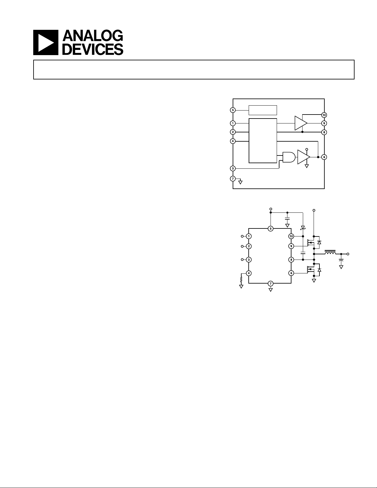
FUNCTIONAL BLOCK DIAGRAM
VCC
IN
SD
DLY
DRVLSD
GND
FROM DUTY RATIO
MODULATOR
FROM SYSTEM
ENABLE CONTROL
FROM SYSTEM
STATE LOGIC
Figure 1. Typical Application Circuit
UVLO
OVERLAP
PROTECTION
CIRCUIT
5V
VCC
IN
SD
ADP3415
DRVLSD
DLY
GND
BST
DRVH
SW
DRVL
ADP3415
VCC
V
DCIN
BST
DRVH
SW
DRVL
V
OUT
REV. B
Information furnished by Analog Devices is believed to be accurate and
reliable. However, no responsibility is assumed by Analog Devices for its
use, nor for any infringements of patents or other rights of third parties that
may result from its use. No license is granted by implication or otherwise
under any patent or patent rights of Analog Devices. Trademarks and
registered trademarks are the property of their respective owners.
One Technology Way, P.O. Box 9106, Norwood, MA 02062-9106, U.S.A.
Tel: 781/329-4700 www.analog.com
Fax: 781/326-8703 © 2004 Analog Devices, Inc. All rights reserved.
Page 2

ADP3415–SPECIFICATIONS
(TA = 0ⴗC to 100ⴗC, VCC = 5 V, V
1
unless otherwise noted.)
– VSW = 5 V, SD = 5 V, C
BST
DRVH
= C
DRVL
= 3 nF,
Parameter Symbol Conditions Min Typ Max Unit
SUPPLY (VCC)
Quiescent Current
2
I
CCQ
Shutdown Mode VSD = 0.8 V 30 65 µA
Operating Mode VSD = 5 V, No Switching 1.2 2 mA
UNDERVOLTAGE LOCKOUT
(UVLO)
UVLO Threshold V
UVLO Hysteresis V
CCUVLO
CCHUVLO
3.9 4.15 4.5 V
0.05 V
LOW-SIDE DRIVER SHUTDOWN
(DRVLSD)
Input Voltage High
Input Voltage Low
Propagation Delay
(See Figure 3) tpdh
SHUTDOWN (SD)
Input Voltage High
Input Voltage Low
INPUT (IN)
Input Voltage High
Input Voltage Low
3
3, 4
3
3
3
3
3
V
IH
V
IL
tpdl
V
IH
V
IL
V
IH
V
IL
DRVLSD
DRVLSD
2.0 V
0.8 V
20 50 ns
10 30 ns
2.0 V
0.8 V
2.0 V
0.8 V
THERMAL SHUTDOWN (THSD)
THSD Threshold T
THSD Hysteresis T
SD
HSD
TJ = T
TJ = T
A
A
165 °C
10 °C
HIGH-SIDE DRIVER (DRVH)
Output Resistance, DRVH–BST 1.5 3.5 Ω
Output Resistance, DRVH–SW 0.85 2.0 Ω
DRVH Transition Times
(See Figure 4) tf
DRVH Propagation Delay
(See Figure 4) tpdl
4
4, 5
tr
DRVH
DRVH
tpdh
DRVH
DRVH
V
– VSW = 4.6 V 20 30 ns
BST
25 35 ns
V
– VSW = 4.6 V, V
BST
R
≥ 120 kΩ 100 200 ns
DLY
= 0 V 10 22 40 ns
DLY
40 70 ns
LOW-SIDE DRIVER (DRVL)
Output Resistance, DRVL–VCC 1.6 3.0 Ω
Output Resistance, DRVL–GND 1.0 3.0 Ω
DRVL Transition Times
(See Figure 4) tf
DRVL Propagation Delay
(See Figure 4) tpdl
SW Transition Timeout
Zero-Crossing Threshold V
NOTES
1
All limits at temperature extremes are guaranteed via correlation using standard Statistical Quality Control (SQC) methods.
2
Including I
3
The signal source driving the pin must have 70 µA (typ) pull-down strength to make a high-to-low transient, and 20 µA (typ) pull-up strength to make a low-to-high
transient. The pin does not represent load (<100 nA) in static low (<0.8 V) and static high (>2.0 V) logic states (see TPC 3.) The pin can be driven with standard
TTL logic level source.
4
Guaranteed by characterization.
5
For propagation delays, tpdh refers to the specified signal going high, tpdl refers to it going low.
6
Propagation delay measured until DRVL begins its transition.
7
The turn-on of DRVL is initiated after IN goes low by either VSW crossing a ~1.6 V threshold or by expiration of t
Specifications subject to change without notice.
quiescent current.
BSTQ
4
7
4, 5, 6
tr
DRVL
DRVL
tpdh
t
SWTO
ZC
DRVL
DRVL
V
– VSW = 4.6 V 25 40 ns
BST
V
– VSW = 4.6 V 20 30 ns
BST
V
– VSW = 4.6 V 10 30 38 ns
BST
V
– VSW = 4.6 V 10 25 ns
BST
V
– VSW = 4.6 V 130 300 ns
BST
1.6 V
.
SWTO
REV. B–2–
Page 3
ADP3415
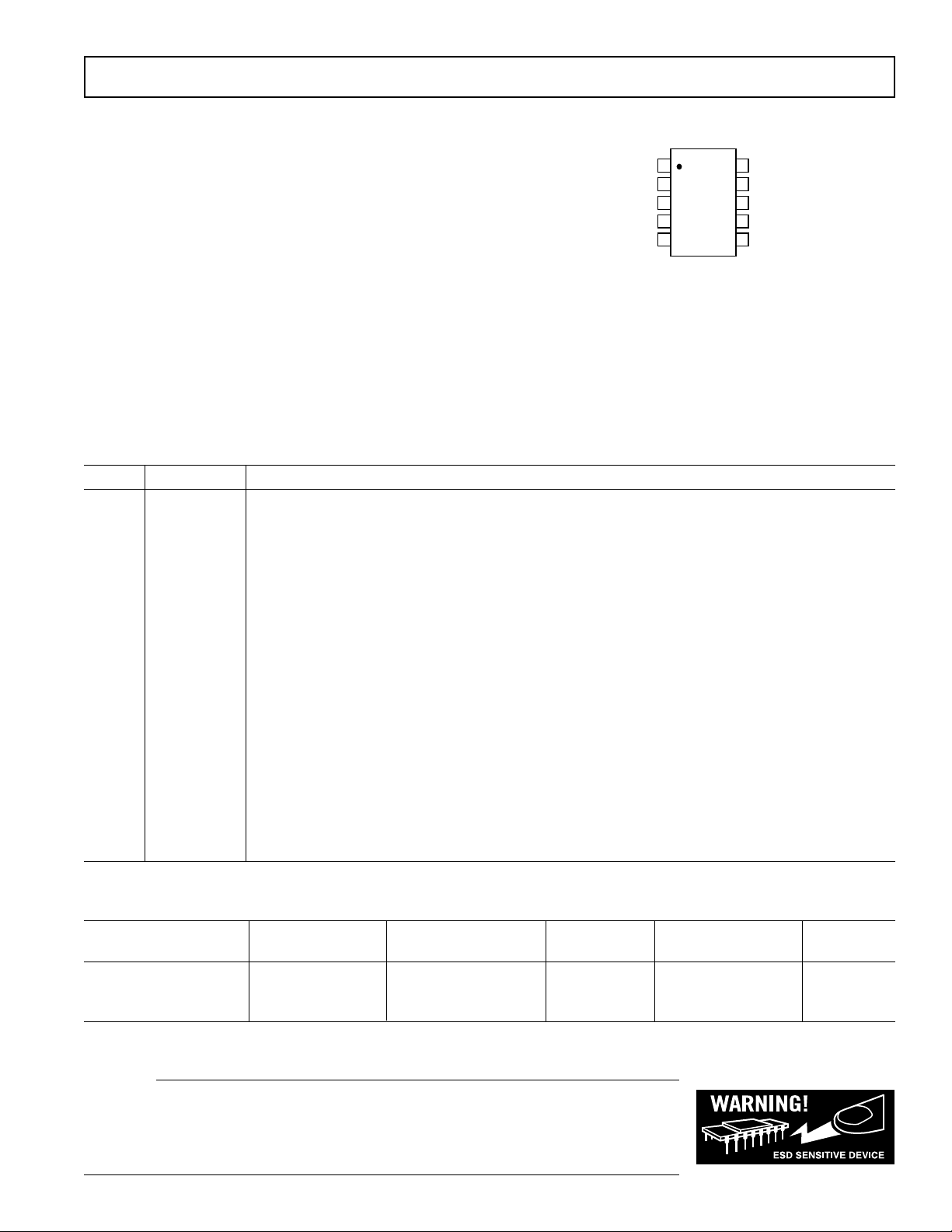
TOP VIEW
(Not to Scale)
10
9
8
7
6
1
2
3
4
5
IN
SD
DRVLSD
DLY
BST
DRVH
SW
GND
ADP3415
VCC
DRVL
ABSOLUTE MAXIMUM RATINGS*
PIN CONFIGURATION
VCC to GND . . . . . . . . . . . . . . . . . . . . . . . . . –0.3 V to +7 V
BST to GND . . . . . . . . . . . . . . . . . . . . . . . . . –0.3 V to +30 V
BST to SW . . . . . . . . . . . . . . . . . . . . . . . . . . . –0.3 V to +7 V
SW to GND . . . . . . . . . . . . . . . . . . . . . . . . . –2.0 V to +25 V
SD, IN, DRVLSD to GND . . . . . . . . . . . . . . –0.3 V to +7.3 V
Operating Ambient Temperature Range . . . . . . 0°C to 100°C
Operating Junction Temperature Range . . . . . . 0°C to 125°C
. . . . . . . . . . . . . . . . . . . . . . . . . . . . . . . . . . . . . . 155°C/W
JA
. . . . . . . . . . . . . . . . . . . . . . . . . . . . . . . . . . . . . . . 40°C/W
JC
Storage Temperature Range . . . . . . . . . . . . –65°C to +150°C
Lead Temperature (Soldering, 10 sec) . . . . . . . . . . . . . 300°C
*Stresses above those listed under Absolute Maximum Ratings may cause perma-
nent damage to the device. This is a stress rating only; functional operation of the
device at these or any other conditions above those listed in the operational
sections of this specification is not implied. Exposure to absolute maximum rating
conditions for extended periods may affect device reliability. Absolute maximum
ratings apply individually only, not in combination. Unless otherwise specified, all
other voltages are referenced to GND.
PIN FUNCTION DESCRIPTIONS
Pin No. Mnemonic Function
1IN TTL-Level Input Signal. Has primary control of the drive outputs.
2 SD Shutdown. When high, this pin enables normal operation. When low, DRVH and DRVL are forced low
and the supply current (I
) is minimized as specified.
CCQ
3 DRVLSD Drive-Low Shutdown. When DRVLSD is low, DRVL is kept low. When DRVLSD is high, DRVL is
enabled and controlled by IN and by the adaptive OPC function.
4 DLY High-Side Turn-On Delay. A resistor from this pin to ground programs an extended delay from turn-off
of the lower FET to turn-on of the upper FET.
5 VCC Input Supply. This pin should be bypassed to GND with a ~10 µF ceramic capacitor.
6 DRVL Synchronous Rectifier Drive. Output drive for the lower (synchronous rectifier) FET.
7GND Ground. Should be directly connected to the ground plane, close to the source of the lower FET.
8SWThis pin should be connected to the buck switching node, close to the upper FET’s source. It is the
floating return for the upper FET drive signal. Also, it is used to monitor the switched voltage for the
OPC function.
9 DRVH Buck Drive. Output drive for the upper (buck) FET.
10 BST Floating Bootstrap Supply for the Upper FET. A capacitor connected between BST and SW pins holds
this bootstrapped supply voltage for the high-side FET driver as it is switched. The capacitor should be
an MLC type and should have substantially greater capacitance (e.g., ~ 20×) than the input capacitance
of the upper FET.
ORDERING GUIDE
Temperature Package Package Quantity
Model Guide Description Option per Reel Branding
ADP3415LRM-REEL 0°C to 100°C MSOP RM-10 3,000 P1E
ADP3415LRM-REEL7 0°C to 100°C MSOP RM-10 1,000 P1E
ADP3415LRMZ-REEL* 0°C to 100°C MSOP RM-10 3,000 P1E
*Z = Pb-free part.
CAUTION
ESD (electrostatic discharge) sensitive device. Electrostatic charges as high as 4000 V readily
accumulate on the human body and test equipment and can discharge without detection. Although the
ADP3415 features proprietary ESD protection circuitry, permanent damage may occur on devices
–3–
subjected to high energy electrostatic discharges. Therefore, proper ESD precautions are recommended
to avoid performance degradation or loss of functionality.
REV. B
Page 4
ADP3415
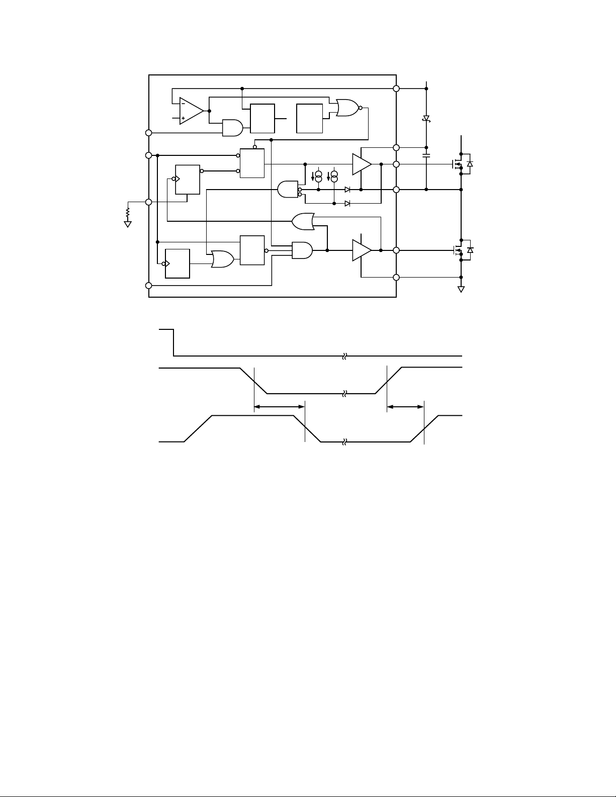
D
R
DLY
DRVLSD
SD
DLY
VCC
VCC
UVLO
V
UVLOTH
IN
DRVH
T
ON
DLY
SET
DRVL
T
ON
DLY
R
S
R
S
EN
CLR
BIAS
Q
Q
BIAS
THERM
SD
THSD
VCC
VTOK
BST
DRVH
SW
DRVL
GND
D
BST
V
DCIN
+
C
BST
Q1
Q2
ADP3415
Figure 2. Functional Block Diagram
IN
RVLSD
DRVL
Figure 3.
DRVLSD
tpdl
DRVLSD
Propagation Delay
tpdh
DRVLSD
REV. B–4–
Page 5

ADP3415
IN
DRVL
DRVH-SW
tpdl
DRVL
tf
DRVL
tpdh
DRVH
tr
DRVH
tpdl
DRVH
tf
DRVH
tr
DRVL
tpdh
DRVL
Figure 4. Switching Timing Diagram (Propagation Delay Referenced to 50%, Rise and Fall Time to 10% and 90% Points)
IN
t
SWTO
DRVL
CROWBAR
ACT ION
SW
DRVH
Figure 5. Switching Waveforms–SW Node Failure Mode–DRVL Timeout
REV. B
–5–
Page 6

ADP3415–Typical Performance Characteristics
2V/DIV
DRVH
DRVL
IN
VCC = 5V
C
= 3nF
LOAD
= 0V
20ns/DIV
TIME – ns
TPC 1. DRVH Fall and DRVL Rise Times
2V/DIV
DRVL
V
SW
TPC 4. DRVL Rise and Fall Times vs. Temperature
37
VCC = 5V
C
= 3nF
LOAD
35
33
31
29
TIME – ns
27
25
23
21
0 12525 50 75 100
30
VCC = 5V
C
LOAD
28
26
JUNCTION TEMPERATURE – ⴗC
= 3nF
RISE TIME
FA LL TIME
FA LL TIME
DRVH
IN
VCC = 5V
= 3nF
C
LOAD
= 40k⍀
20ns/DIV
TIME – ns
R
DLY
TPC 2. DRVL Fall and DRVH Rise Times
100
VCC = 5V
90
= 25ⴗC
T
A
C
= 3nF
LOAD
80
70
60
50
40
30
PEAK CURRENT – A
20
10
0
05
HIGH-TO-LOW TRANSITION
LOW-TO-HIGH TRANSITION
1234
INPUT VOLTAGE – V
TPC 3. Input Voltage vs. Input Current
24
22
TIME – ns
20
18
16
0 12525 50
JUNCTION TEMPERATURE – ⴗC
TPC 5. DRVH Rise and Fall Times vs. Temperature
70
VCC = 5V
T
= 25ⴗC
A
60
50
40
TIME – ns
30
20
10
1103579
2468
LOAD CAPACITANCE – nF
TPC 6. DRVH and DRVL Rise Time vs. Load Capacitance
RISE TIME
75 100
DRVL
DRVH
REV. B–6–
Page 7

ADP3415
52
VCC = 5V
C
= 3nF
LOAD
47
42
37
32
27
TIME – ns
22
17
12
7
2
0 12525 50 75 100
tpdl
DRVH
tpdl
DRVL
JUNCTION TEMPERATURE – ⴗC
TPC 7. DRVH and DRVL Propagation Delay
vs. Temperature
52
VCC = 5V
T
= 25ⴗC
A
47
42
37
32
27
TIME – ns
22
17
12
7
24 79
1103568
DRVH
DRVL
LOAD CAPACITANCE – nF
TPC 8. DRVH and DRVL Fall Time vs. Load Capacitance
45
VCC = 5V
T
= 25ⴗC
A
40
C
= 3nF
LOAD
35
30
25
20
15
SUPPLY CURRENT – mA
10
5
0
200 1200
400 600 800 1000
IN FREQUENCY – kHz
TPC 10. Supply Current vs. Frequency
10.5
10.0
9.5
9.0
8.5
8.0
7.5
SUPPLY CURRENT – mA
7.0
VCC = 5V
f
= 250kHz
IN
6.5
6.0
= 3nF
C
LOAD
0 125
25 50 75 100
JUNCTION TEMPERATURE – ⴗC
TPC 11. Supply Current vs. Temperature
REV. B
182
VCC = 5V
f
= 200kHz
IN
162
C
= 3nF
LOAD
142
OPEN DELAY PIN
122
102
82
TIME – ns
62
42
SHORTED TO GROUND
22
2
0 125
25 50 75 100
JUNCTION TEMPERATURE – ⴗC
TPC 9. tpdh
vs. Temperature
DRVH
–7–
Page 8

ADP3415
THEORY OF OPERATION
The ADP3415 is a dual MOSFET driver optimized for driving
two N-channel FETs in a synchronous buck converter topology.
A single duty ratio modulation signal is all that is required to
command the proper drive signal for the high-side and the
low-side FETs.
A more detailed description of the ADP3415 and its features
follows. Refer to the Functional Block Diagram (Figure 2).
Drive State Input
The drive state input, IN, should be connected to the duty ratio
modulation signal of a switch-mode controller. IN can be driven
by 2.5 V to 5.0 V logic. The FETs will be driven so that the SW
node follows the polarity of IN.
Low-Side Driver
The supply rails for the low-side driver, DRVL, are VCC and
GND. In its conventional application, it drives the gate of the
synchronous rectifier FET.
When the driver is enabled, the driver’s output is 180° out of
phase with the duty ratio input aside from overlap protection
circuit, propagation, and transition delays. When the driver is
shut down or the entire ADP3415 is in shutdown or in undervoltage lockout, the low-side gate is held low.
High-Side Driver
The supply rail for the high-side driver, DRVH, is between the
BST and SW pins and is created by an external bootstrap supply circuit. In its conventional application, it drives the gate of
the (top) main buck converter FET.
The bootstrap circuit comprises a Schottky diode, D
bootstrap capacitor, C
. When the ADP3415 is starting up,
BST
BST
, and
the SW pin is at ground, so the bootstrap capacitor will charge
up to VCC through DBST. As the supply voltage ramps up and
exceeds the UVLO threshold, the driver is enabled. When the
input pin, IN, goes high, the high-side driver will begin to turn
the high-side FET (Q1) ON by transferring charge from C
BST
to
the gate of the FET. As Q1 turns ON, the SW pin will rise up to
V
, forcing the BST pin to V
DCIN
DCIN
+ V
, which is enough
C(BST)
gate to source voltage to hold Q1 ON. To complete the cycle,
when IN goes low, Q1 is switched OFF as DRVH discharges
the gate to the voltage at the SW pin. When the low-side FET,
Q2, turns ON, the SW pin is held at ground. This allows the
bootstrap capacitor to charge up to VCC again.
The high-side driver’s output is in phase with the duty ratio
input. When the driver is in undervoltage lockout, the high-side
gate is held low.
Overlap Protection Circuit
The overlap protection circuit (OPC) prevents both of the main
power switches, Q1 and Q2, from being ON at the same time.
This prevents excessive shoot-through currents from flowing
through both power switches and minimizes the associated
losses that can occur during their ON-OFF transitions. The
overlap protection circuit accomplishes this by adaptively
controlling the delay from Q1’s turn OFF to Q2’s turn ON and
by programming the delay from Q2’s turn OFF to Q1’s turn ON.
To prevent the overlap of the gate drives during Q1’s turn OFF
and Q2’s turn ON, the overlap circuit monitors the voltage at
the SW pin. When IN goes low, Q1 will begin to turn OFF
(after a propagation delay), but before Q2 can turn ON, the
overlap protection circuit waits for the voltage at the SW pin to
fall from V
to 1.6 V. Once the voltage on the SW pin has
DCIN
fallen to 1.6 V, Q2 will begin to turn ON. By waiting for the
voltage on the SW pin to reach 1.6 V, the overlap protection
circuit ensures that Q1 is OFF before Q2 turns on, regardless of
variations in temperature, supply voltage, gate charge, and drive
current. There is, however, a timeout circuit that will override
the waiting period for the SW pin to reach 1.6 V. After the
timeout period has expired, DRVL will be asserted regardless of
the SW voltage.
To prevent the overlap of the gate drives during Q2’s turn OFF
and Q1’s turn ON, the overlap circuit provides a programmable
delay that is set by a resistor on the DLY pin. When IN goes
high, Q2 will begin to turn OFF (after a propagation delay), but
before Q1 can turn ON, the overlap protection circuit waits for
the voltage at DRVL to go low. Once the voltage at DRVL is
low, the overlap protection circuit initiates a delay timer that is
programmed by the external resistor R
. The delay resistor
DLY
adds an additional specified delay. The delay allows time for
current to commutate from the body diode of Q2 to an external
Schottky diode, which allows turn-off losses to be reduced.
Although not as foolproof as the adaptive delay, the programmable delay adds a safety margin to account for variations in size,
gate charge, and internal delay of the external power MOSFETs.
Low-Side Driver Shutdown
The low-side driver shutdown, DRVLSD, allows a control
signal to shut down the synchronous rectifier. This signal should
be modulated by system state logic to achieve maximum battery
life under light load conditions and maximum efficiency under
heavy load conditions. Under heavy load conditions, DRVLSD
should be high so that the synchronous switch is modulated for
maximum efficiency. Under light load conditions, DRVLSD
should be low to prevent needless switching losses due to charge
shuttling caused by polarity reversal of the inductor current
when the average current is low.
When the DRVLSD input is low, the low-side driver stays low.
When the DRVLSD input is high, the low-side driver is enabled
and controlled by the driver signals as previously described.
Low-Side Driver Timeout Circuit
In normal operation, the DRVH signal tracks the IN signal
and turns OFF the Q1 high-side switch with a few tens of ns
tpdl
delay following the falling edge of the input signal.
DRVH
When Q1 is turned OFF, then DRVL is allowed to go high,
Q2 to turn ON, and the SW node voltage to collapse to zero.
But in a faulty scenario, such as the case of a high-side Q1
switch drain-source short circuit when even DRVH goes low,
the SW node cannot fall to zero.
The ADP3415 has a timer circuit to address this scenario. Every
time the IN goes low, a DRVL on-time delay timer gets triggered (see Figure 2). Should the SW node voltage not trigger
the low side turn-on, the DRVL on-time delay circuit will do it
instead, when it times out with t
delay (see Figure 5). If the
SWTO
high-side Q1 is still turned ON, i.e., its drain is shorted to the
source, the low-side Q2 turn-on will create a direct short circuit
across the V
the fuse in the V
voltage rail, and the crowbar action will blow
DCIN
current patch. The opening of the fuse saves
DCIN
the load (CPU) from potential damage that the high-side switch
short circuit could have caused.
REV. B–8–
Page 9

ADP3415
Shutdown
For optimal system power management, when the output voltage
is not needed, the ADP3415 can be shut down to conserve power.
When the SD pin is high, the ADP3415 is enabled for normal
operation. Pulling the SD pin low forces the DRVH and DRVL
outputs low, turning the buck converter OFF and reducing the
VCC supply current to less than 40 µA.
Undervoltage Lockout
The undervoltage lockout (UVLO) circuit holds both FET
driver outputs low during VCC supply ramp-up. The UVLO
logic becomes active and in control of the driver outputs at a
supply voltage of no greater than 1.5 V. The UVLO circuit
waits until the VCC supply has reached a voltage high enough
to bias logic level FETs fully ON, around 4.1 V, before releasing control of the drivers to the control pins.
Thermal Shutdown
The thermal shutdown circuit protects the ADP3415 against
damage due to excessive power dissipation. Under extreme
conditions, high ambient temperature and high power dissipation, the die temperature may rise up to the thermal shutdown
threshold of 165°C. If the die temperature exceeds 165°C, the
thermal shutdown circuit will turn the output drivers OFF. The
drivers remain disabled until the junction temperature has
decreased by 10°C, at which point the drivers are again enabled.
APPLICATION INFORMATION
Supply Capacitor Selection
For the supply input (VCC) of the ADP3415, a local bypass
capacitor is recommended to reduce the noise and to supply
some of the peak currents drawn. Use a 10 µF MLC capacitor.
Keep the ceramic capacitor as close as possible to the ADP3415.
Multilayer ceramic (MLC) capacitors provide the best combination of low ESR and small size and can be obtained from the
following vendors:
Murata GRM235Y5V106Z16 www.murata.com
Taiyo-Yuden EMK325F106ZF www.t-yuden.com
Tokin C23Y5V1C106ZP www.tokin.com
Bootstrap Circuit
The bootstrap circuit requires a charge storage capacitor, C
BST
,
and a Schottky diode, D1, as shown in Figure 2. Selecting these
components can be done after the high-side FET has been chosen.
The bootstrap capacitor must have a voltage rating that is able
to handle the maximum battery voltage plus 5 V. The capacitance is determined using the following equation
Q
C
BST
where Q
and ⌬V
GATE
=
V
∆
BST
is the total gate charge of the high-side FET,
GATE
is the voltage droop allowed on the high-side FET
BST
(1)
drive. For example, the IRFR8503 has a total gate charge of
about 15 nC. For an allowed droop of 150 mV, the required
bootstrap capacitance is 100 nF. Use an MLC capacitor.
A Schottky diode is recommended for the bootstrap diode due
to its low forward drop, which maximizes the drive available for
the high-side FET. The bootstrap diode must also be able to
withstand the maximum battery voltage plus 5 V. The average
forward current can be estimated by
IQf
where f
Delay Resistor Selection
The delay resistor, R
≈×
F AVG GATE MAX()
is the maximum switching frequency of the controller.
MAX
, is used to add an additional delay
DLY
(2)
when the low-side FET drive turns off and when the high-side
drive starts to turn on. The delay resistor programs a specified
additional delay besides the 20 ns of fixed delay.
Printed Circuit Board Layout Considerations
Use the following general guidelines when designing printed
circuit boards:
1. Trace out the high current paths and use short, wide traces
to make these connections.
2. Locate the VCC bypass capacitor as close as possible to the
VCC and GND pins.
REV. B
–9–
Page 10

ADP3415
OUTLINE DIMENSIONS
10-Lead Micro Small Outline Package [MSOP]
(RM-10)
Dimensions shown in millimeters
3.00 BSC
6
10
5
4.90 BSC
1.10 MAX
SEATING
PLANE
0.23
0.08
8ⴗ
0ⴗ
3.00 BSC
PIN 1
0.95
0.85
0.75
0.15
0.00
COPLANARITY
1
0.50 BSC
0.27
0.17
0.10
COMPLIANT TO JEDEC STANDARDS MO-187BA
0.80
0.60
0.40
REV. B–10–
Page 11

ADP3415
Revision History
Location Page
1/04—Data Sheet changed from REV. A to REV. B.
Updated ORDERING GUIDE . . . . . . . . . . . . . . . . . . . . . . . . . . . . . . . . . . . . . . . . . . . . . . . . . . . . . . . . . . . . . . . . . . . . . . . . . . . . . 3
Updated OUTLINE DIMENSIONS . . . . . . . . . . . . . . . . . . . . . . . . . . . . . . . . . . . . . . . . . . . . . . . . . . . . . . . . . . . . . . . . . . . . . . . 10
1/03—Data Sheet changed from REV. 0 to REV. A.
Edits to GENERAL DESCRIPTION . . . . . . . . . . . . . . . . . . . . . . . . . . . . . . . . . . . . . . . . . . . . . . . . . . . . . . . . . . . . . . . . . . . . . . . . 1
Edits to SPECIFICATIONS . . . . . . . . . . . . . . . . . . . . . . . . . . . . . . . . . . . . . . . . . . . . . . . . . . . . . . . . . . . . . . . . . . . . . . . . . . . . . . . 2
Edits to ORDERING GUIDE . . . . . . . . . . . . . . . . . . . . . . . . . . . . . . . . . . . . . . . . . . . . . . . . . . . . . . . . . . . . . . . . . . . . . . . . . . . . . . 3
Updated OUTLINE DIMENSIONS . . . . . . . . . . . . . . . . . . . . . . . . . . . . . . . . . . . . . . . . . . . . . . . . . . . . . . . . . . . . . . . . . . . . . . . 10
REV. B
–11–
Page 12

C01681–0–1/04(B)
–12–
 Loading...