

Page 1
Dual Bootstrapped MOSFET Driver
a
FEATURES
All-In-One Synchronous Buck Driver
Bootstrapped High Side Drive
One PWM Signal Generates Both Drives
Anticross-Conduction Protection Circuitry
Pulse-by-Pulse Disable Control
APPLICATIONS
Multiphase Desktop CPU Supplies
Mobile Computing CPU Core Power Converters
Single-Supply Synchronous Buck Converters
Standard-to-Synchronous Converter Adaptations
GENERAL DESCRIPTION
The ADP3413 is a dual MOSFET driver optimized for driving
two N-channel MOSFETs which are the two switches in a
nonisolated synchronous buck power converter. Each of the
drivers is capable of driving a 3000 pF load with a 20 ns propagation delay and a 30 ns transition time. One of the drivers can
be bootstrapped and is designed to handle the high voltage
slew rate associated with “floating” high side gate drivers.
The ADP3413 includes overlapping drive protection (ODP)
to prevent shoot-through current in the external MOSFETs.
The OD Pin provides high speed control to quickly turn off
both gate drives.
The ADP3413 is specified over the commercial temperature
range of 0°C to 70°C and is available in an 8-lead SOIC package.
ADP3413
VCC
with Output Disable
ADP3413
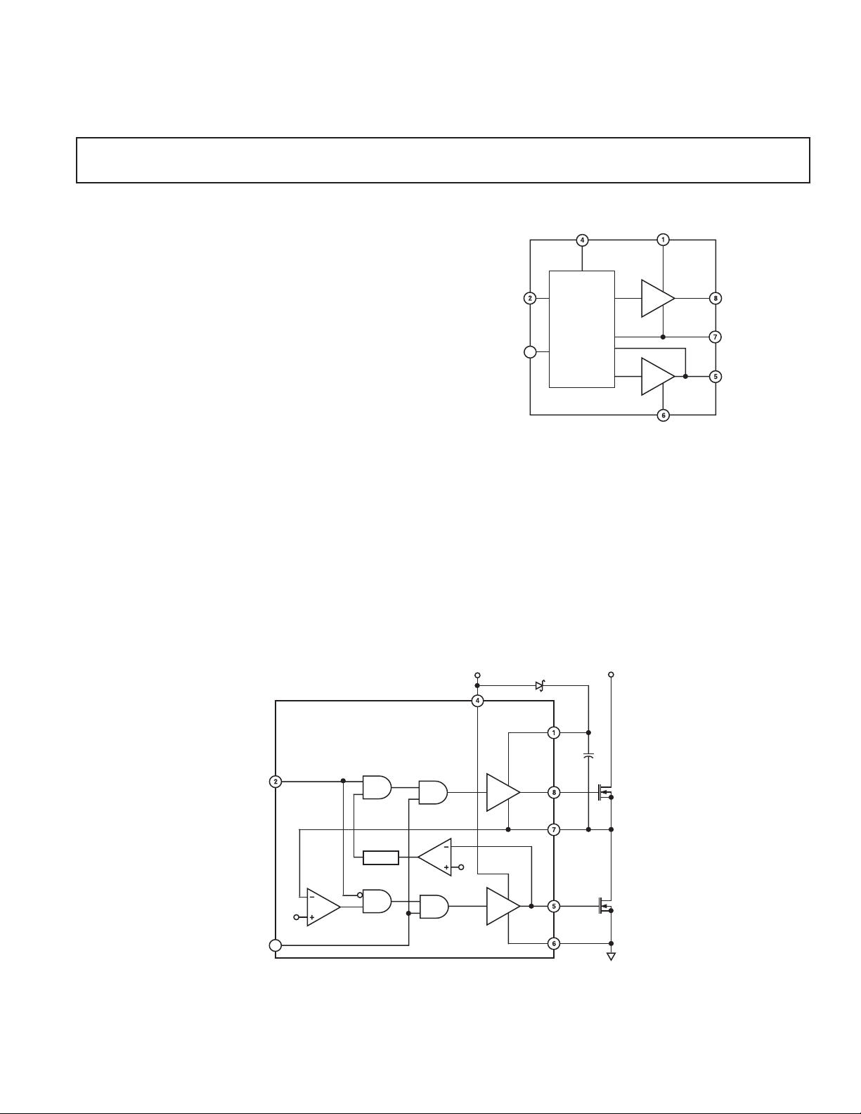
FUNCTIONAL BLOCK DIAGRAM
VCC
IN
OVERLAP
PROTECTION
CIRCUIT
3
OD
ADP3413
7V
D1
BST
12V
BST
DRVH
SW
DRVL
PGND
IN
DELAY
1V
3
OD
REV. A
Information furnished by Analog Devices is believed to be accurate and
reliable. However, no responsibility is assumed by Analog Devices for its
use, nor for any infringements of patents or other rights of third parties that
may result from its use. No license is granted by implication or otherwise
under any patent or patent rights of Analog Devices.
Figure 1. General Application Circuit
C
BST
DRVH
SW
+1V
DRVL
PGND
One Technology Way, P.O. Box 9106, Norwood, MA 02062-9106, U.S.A.
Tel: 781/329-4700 www.analog.com
Fax: 781/326-8703 © Analog Devices, Inc., 2002
Q1
Q2
Page 2

1
ADP3413–SPECIFICATIONS
Parameter Symbol Conditions Min Typ Max Unit
SUPPLY
Supply Voltage Range VCC 4.15 7.5 V
Quiescent Current ICC
OD INPUT
Input Voltage High
Input Voltage Low
2
2
Propagation Delay Time tpdl
PWM INPUT
Input Voltage High
Input Voltage Low
2
2
HIGH SIDE DRIVER
Output Resistance, Sourcing Current V
Output Resistance, Sinking Current V
Transition Times
Propagation Delay
3
(See Figure 2) tr
3, 4
(See Figure 2) tpdh
LOW SIDE DRIVER
Output Resistance, Sourcing Current VCC = 5 V 3.0 5.0 Ω
Output Resistance, Sinking Current VCC = 5 V 1.5 3.0 Ω
3
Transition Times
Propagation Delay
NOTES
1
All limits at temperature extremes are guaranteed via correlation using standard Statistical Quality Control (SQC) methods.
2
Logic inputs meet typical CMOS I/O conditions for source/sink current (~1 µA).
3
AC specifications are guaranteed by characterization but not production tested.
4
For propagation delays, “tpdh” refers to the specified signal going high; “tpdl” refers to it going low.
Specifications subject to change without notice.
(See Figure 2) tr
3, 4
(See Figure 2) tpdh
tpdh
DRVH
tf
DRVH
tpdl
DRVL
tf
DRVL
tpdl
Q
OD
OD
DRVH
DRVH
DRVL
DRVL
(TA = 0ⴗC to 70ⴗC, VCC = 7 V, BST = 4 V to 26 V, OD > 2 V, unless otherwise noted.)
12 mA
2.0 V
0.8 V
15 30 ns
15 30 ns
2.3 V
0.8 V
– VSW = 5 V 3.0 5.0 Ω
BST
V
– VSW = 7 V 2.0 3.5 Ω
BST
– VSW = 5 V 1.25 2.5 Ω
BST
– VSW = 7 V 1.0 2.5 Ω
V
BST
V
– VSW = 7 V, C
BST
V
– VSW = 7 V, C
BST
V
– V
BST
BST
– V
SW
SW
V
= 7 V 65 86 ns
= 7 V 22 32 ns
= 3 nF 36 47 ns
LOAD
= 3 nF 20 30 ns
LOAD
VCC = 7 V 2.0 3.5 Ω
VCC = 7 V 1.0 2.5 Ω
VCC = 7 V, C
VCC = 7 V, C
= 3 nF 27 35 ns
LOAD
= 3 nF 19 26 ns
LOAD
VCC = 7 V 30 35 ns
VCC = 7 V 17 25 ns
–2–
REV. A
Page 3
ADP3413
ABSOLUTE MAXIMUM RATINGS*
VCC . . . . . . . . . . . . . . . . . . . . . . . . . . . . . . . . –0.3 V to +8 V
BST . . . . . . . . . . . . . . . . . . . . . . . . . . . . . . . . –0.3 V to +30 V
BST to SW . . . . . . . . . . . . . . . . . . . . . . . . . . . –0.3 V to +8 V
SW . . . . . . . . . . . . . . . . . . . . . . . . . . . . . . . . –5.0 V to +25 V
OD, IN . . . . . . . . . . . . . . . . . . . . . . . . –0.3 V to VCC + 0.3 V
Model Range Description Option
ADP3413JR 0°C to 70°C8-Lead Standard SOIC-8
ORDERING GUIDE
Temperature Package Package
Small Outline (SOIC)
Operating Ambient Temperature Range . . . . . . . 0°C to 70°C
Operating Junction Temperature Range . . . . . . 0°C to 125°C
. . . . . . . . . . . . . . . . . . . . . . . . . . . . . . . . . . . . . . . 155°C/W
θ
JA
. . . . . . . . . . . . . . . . . . . . . . . . . . . . . . . . . . . . . . . . 40°C/W
θ
JC
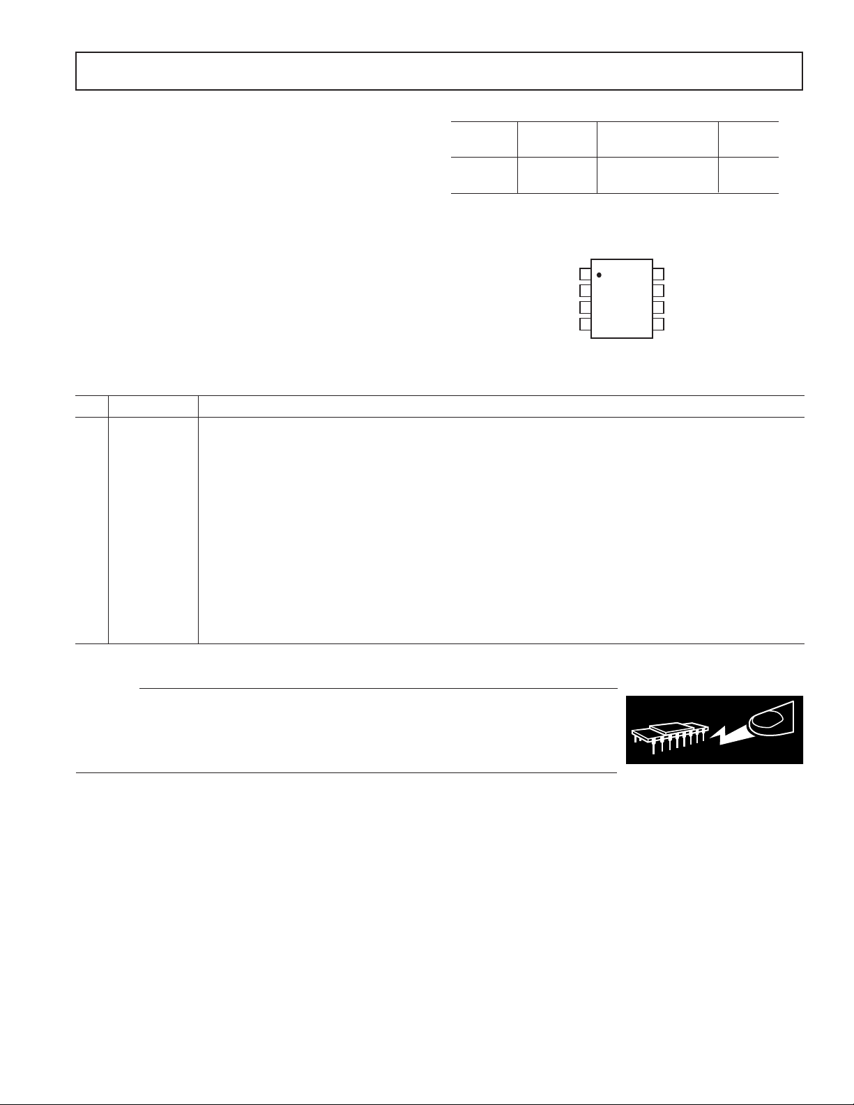
PIN CONFIGURATION
Storage Temperature Range . . . . . . . . . . . . –65°C to +150°C
Lead Temperature (Soldering, 10 sec) . . . . . . . . . . . . . 300°C
*This is a stress rating only; operation beyond these limits can cause the device to
be permanently damaged. Unless otherwise specified, all voltages are referenced
to PGND.
BST
OD
VCC
IN
2
ADP3413
3
TOP VIEW
(Not To Scale)
4
8
7
6
5
DRVH
SW
PGND
DRVL
1
PIN FUNCTION DESCRIPTIONS
Pin Mnemonic Function
1 BST Floating Bootstrap Supply for the Upper MOSFET. A capacitor connected between BST and SW Pins
holds this bootstrapped voltage for the high side MOSFET as it is switched. The capacitor should be
chosen between 100 nF and 1 F.
2IN TTL-level input signal that has primary control of the drive outputs.
3 OD Output Disable. When low, this pin disables normal operation, forcing DRVH and DRVL low.
4 VCC Input Supply. This pin should be bypassed to PGND with ~1 µF ceramic capacitor.
5 DRVL Synchronous Rectifier Drive. Output drive for the lower (synchronous rectifier) MOSFET.
6 PGND Power Ground. Should be closely connected to the source of the lower MOSFET.
7SW This pin is connected to the buck-switching node, close to the upper MOSFET’s source. It is the floating
return for the upper MOSFET drive signal. It is also used to monitor the switched voltage to prevent turnon of the lower MOSFET until the voltage is below ~1 V. Thus, according to operating conditions, the
high low transition delay is determined at this pin.
8 DRVH Buck Drive. Output drive for the upper (buck) MOSFET.
CAUTION
ESD (electrostatic discharge) sensitive device. Electrostatic charges as high as 4000 V readily
accumulate on the human body and test equipment and can discharge without detection. Although
the ADP3413 features proprietary ESD protection circuitry, permanent damage may occur on
devices subjected to high energy electrostatic discharges. Therefore, proper ESD precautions are
recommended to avoid performance degradation or loss of functionality.
REV. A
–3–
WARNING!
ESD SENSITIVE DEVICE
Page 4
ADP3413
DRVL
IN
DRVL
tf
DRVL
tpdh
DRVHtrDRVH
tpdl
DRVH
tf
DRVH
tr
DRVL
tpdl
DRVH-SW
SW
V
TH
V
TH
tpdh
DRVL
1V
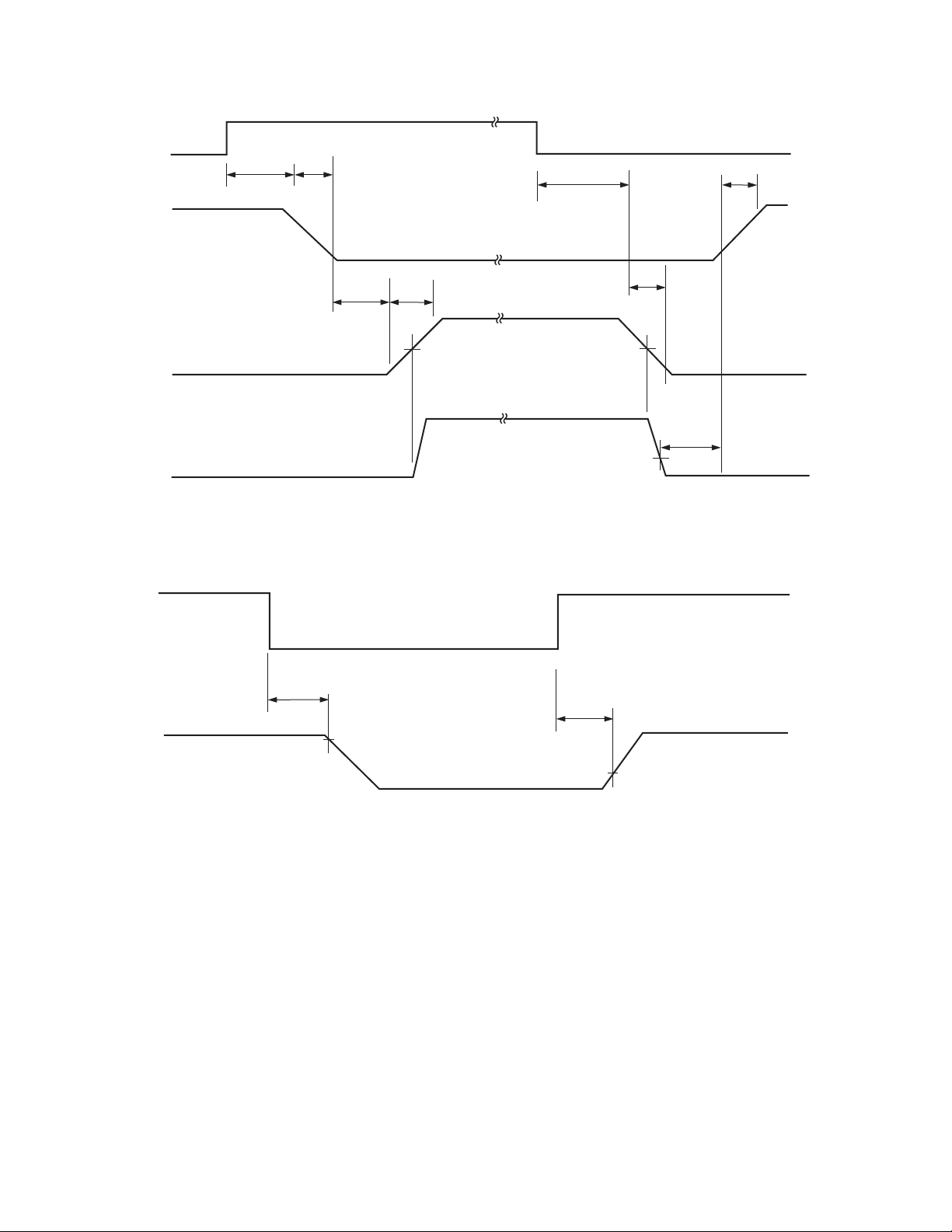
Figure 2. Nonoverlap Timing Diagram (Timing Is Referenced to the 90% and 10% Points Unless Otherwise Noted)
OD
tpdl
DRVH
OR
DRVL
OD
90%
tpdh
OD
10%
Figure 3. Output Disable Timing Diagram
–4–
REV. A
Page 5

Typical Performance Characteristics–
ADP3413
R3
R2
R1
DRVH
5V/DIV
IN
2V/DIV
T
T
= 25ⴗC
A
VCC = 5V
DRVL
5V/DIV
40ns/DIV
TPC 1. DRVH Fall and DRVL Rise
Times
35
30
25
20
15
TIME – ns
10
5
0
0
DRVL @ VCC = 5V
25
JUNCTION TEMPERATURE – ⴗC
DRVL @ VCC = 7V
DRVH @ VCC = 7V
DRVH @ VCC = 5V
50 75 100
125
TPC 4. DRVH and DRVL Fall Times
vs. Temperature
T
R3
R2
R1
TA = 25ⴗC
VCC = 5V
IN
2V/DIV
DRVL
2V/DIV
DRVH
5V/DIV
40ns/DIV
TPC 2. DRVL Fall and DRVH Rise
Times
55
50
45
40
35
30
TIME – ns
25
20
15
10
1.0
DRVH @ VCC = 5V
DRVH @ VCC = 7V
DRVL @ VCC = 5V
DRVL @ VCC = 7V
2.0 3.0 4.0 5.0
LOAD CAPACITANCE – nF
TPC 5. DRVH and DRVL Rise Times
vs. Load Capacitance
50
C
= 3nF
LOAD
DRVH @ VCC = 5V
45
40
35
TIME – ns
30
25
20
0
DRVL @ VCC = 5V
25
JUNCTION TEMPERATURE – ⴗC
DRVH @ VCC = 7V
DRVL @ VCC = 7V
50 75
100
125
TPC 3. DRVH and DRVL Rise Times
vs. Temperature
37
32
DRVL @ VCC = 7V
27
22
TIME – ns
17
12
7
1.0
DRVH @ VCC = 7V
DRVL @ VCC = 5V
1.5 2.0 2.5 3.0 3.5 4.0 4.5 5.0
LOAD CAPACITANCE – nF
DRVH @ VCC = 5V
TPC 6. DRVH and DRVL Fall Times
vs. Load Capacitance
35
TA = 25ⴗC
= 3nF
C
30
LOAD
25
20
15
10
SUPPLY CURRENT – mA
5
0
0
VCC
200
400 600 800
IN FREQUENCY – kHz
= 7V
TPC 7. Supply Current vs.
Frequency
VCC = 5V
1000 1200 1400
8.5
8
VCC = 7V
7.5
7
6.5
6
SUPPLY CURRENT – mA
VCC = 5V
5.5
5
0
25 50 75
JUNCTION TEMPERATURE – ⴗC
TPC 8. Supply Current vs.
Temperature
C
LOAD
= 250kHz
f
IN
100
= 3nF
125
REV. A
–5–
Page 6

ADP3413
THEORY OF OPERATION
The ADP3413 is a dual MOSFET driver optimized for driving
two N-channel MOSFETs in a synchronous buck converter
topology. A single PWM input signal is all that is required to
properly drive the high side and the low side FETs. Each driver
is capable of driving a 3 nF load.
A more detailed description of the ADP3413 and its features
follows. Refer to the Functional Block Diagram.
Low Side Driver
The low side driver is designed to drive low R
DS(ON)
N-channel
MOSFETs. The maximum output resistance for the driver is
3.5 Ω for sourcing and 2.5 Ω for sinking gate current. The
low output resistance allows the driver to have 30 ns rise
and fall times into a 3 nF load. The bias to the low side driver is
internally connected to the VCC supply and PGND.
When the driver is enabled, the driver’s output is 180 degrees
out of phase with the PWM input. When the ADP3413 is disabled, the low side gate is held low.
High Side Driver
The high side driver is designed to drive a floating low R
DS(ON)
N-channel MOSFET. The maximum output resistance for the
driver is 3.5 Ω for sourcing and 2.5 Ω for sinking gate current. The low output resistance allows the driver to have 30 ns
rise and fall times into a 3 nF load. The bias voltage for the
high side driver is developed by an external bootstrap supply
circuit, which is connected between the BST and SW Pins.
The bootstrap circuit comprises a diode, D1, and bootstrap
capacitor, C
. When the ADP3413 is starting up, the SW Pin
BST
is at ground, so the bootstrap capacitor will charge up to VCC
through D1. When the PWM input goes high, the high side
driver will begin to turn the high side MOSFET, Q1, ON by
pulling charge out of C
rise up to V
, forcing the BST Pin to VIN + V
IN
. As Q1 turns ON, the SW Pin will
BST
C(BST)
, which is
enough gate to source voltage to hold Q1 ON. To complete the
cycle, Q1 is switched OFF by pulling the gate down to the voltage at the SW Pin. When the low side MOSFET, Q2, turns
ON, the SW Pin is pulled to ground. This allows the bootstrap
capacitor to charge up to VCC again.
The high side driver’s output is in phase with the PWM input.
When the driver is disabled, the high side gate is held low.
Overlap Protection Circuit
The overlap protection circuit (OPC) prevents both of the main
power switches, Q1 and Q2, from being ON at the same time.
This is done to prevent shoot-through currents from flowing
through both power switches and the associated losses that can
occur during their ON-OFF transitions. The overlap protection
circuit accomplishes this by adaptively controlling the delay from
Q1’s turn OFF to Q2’s turn ON and by internally setting the
delay from Q2’s turn OFF to Q1’s turn ON.
To prevent the overlap of the gate drives during Q1’s turn OFF
and Q2’s turn ON, the overlap circuit monitors the voltage at the
SW Pin. When the PWM input signal goes low, Q1 will begin to
turn OFF (after a propagation delay), but before Q2 can turn ON
the overlap protection circuit waits for the voltage at the SW Pin
to fall from V
to 1 V. Once the voltage on the SW Pin has fallen
IN
to 1 V, Q2 will begin turn ON. By waiting for the voltage on the
SW Pin to reach 1 V, the overlap protection circuit ensures that
Q1 is OFF before Q2 turns on, regardless of variations in temperature, supply voltage, gate charge, and drive current.
To prevent the overlap of the gate drives during Q2’s turn OFF
and Q1’s turn ON, the overlap circuit provides a internal delay
that is set to 50 ns. When the PWM input signal goes high, Q2
will begin to turn OFF (after a propagation delay), but before
Q1 can turn ON, the overlap protection circuit waits for the
voltage at DRVL to drop to around 10% of VCC. Once the
voltage at DRVL has reached the 10% point, the overlap protection circuit will wait for a 20 ns typical propagation delay. Once
the delay period has expired, Q1 will begin turn ON.
Output Disable
The disable input is used to turn off the buck converter. If the
circuits running off of the buck converter are not needed, the
ADP3413 can be shutdown to conserve power. When the OD
Pin is low, the ADP3413 is disabled. The DRVH and DRVL
outputs are forced low, turning the buck converter OFF.
APPLICATION INFORMATION
Supply Capacitor Selection
For the supply input (VCC) of the ADP3413, a local bypass
capacitor is recommended to reduce the noise and to supply some
of the peak currents drawn. Use a 1 µF, low ESR capacitor.
Multilayer ceramic chip (MLCC) capacitors provide the best
combination of low ESR and small size and can be obtained from
the following vendors:
Murata GRM235Y5V106Z16 www.murata.com
TaiyoYuden EMK325F106ZF www.t-yuden.com
Tokin C23Y5V1C106ZP www.tokin.com
Keep the ceramic capacitor as close as possible to the ADP3413.
Bootstrap Circuit
The bootstrap circuit uses a charge storage capacitor (C
BST
) and a
Schottky diode, as shown in Figure 1. Selection of these components can be done after the high side MOSFET has been chosen.
The bootstrap capacitor must have a voltage rating that is able
to handle the maximum battery voltage plus 5 V. A minimum 50
V rating is recommended. The capacitance is determined
using the following equation:
Q
GATE
=
∆
V
BST
where, Q
and ∆V
BST
C
BST
is the total gate charge of the high side MOSFET,
GATE
is the voltage droop allowed on the high side MOSFET
drive. For example, the IRF7811 has a total gate charge of about
20 nC. For an allowed droop of 200 mV, the required bootstrap capacitance is 100 nF. A good quality ceramic capacitor
should be used.
A Schottky diode is recommended for the bootstrap diode due
to its low forward drop, which maximizes the drive available for
the high side MOSFET. The bootstrap diode must have a minimum 40 V rating to withstand the maximum battery voltage
plus 5 V. The average forward current can be estimated by:
IQf
≈×
F(AVG) GATE MAX
where f
is the maximum switching frequency of the control-
MAX
ler. The peak surge current rating should be checked in-circuit,
since this is dependent on the source impedance of the 5 V
supply, and the ESR of C
BST
.
–6–
REV. A
Page 7

ADP3413
Printed Circuit Board Layout Considerations
Use the following general guidelines when designing printed
circuit boards:
1. Trace out the high current paths and use short, wide traces
to make these connections.
2. Connect the PGND pin of the ADP3413 as close as possible to the source of the lower MOSFET.
3. The VCC bypass capacitor should be located as close as
possible to VCC and PGND Pins.
34.0k⍀
C
OC
1.4nF
1.1k⍀
11.5k⍀
V
R
12V
RTN
IN
R
A
Z
R
B
100pF
V
IN
C2
FROM
CPU
270F ⴛ 4
OS–CON 16V
U1
ADP3160
VID4 VCC
1
2
VID3
3
VID2
4
VID1
5
VID0
6
COMP
7
PWRGND
FB
8
CT
C1
150pF
R1
1k⍀
C4
4.7F
REF
CS–
PWM1
PWM2
CS+
GND
C15C14C13C12
10⍀
C26
4.7F
R6
C21
15nF
C22
16
1nF
15
14
13
12
11
10
9
R5
2.4k⍀
Z1
ZMM5236BCT
1F
C6
20⍀
MBR052LTI
Q5
2N3904
MBR052LTI
R7
C5
1F
D2
D1
Typical Application Circuits
The circuit in Figure 4 shows how two drivers can be combined with the ADP3160 to form a total power conversion
solution for V
CC(CORE)
generation in a high current Intel CPU
computer. Figure 5 gives a similar application circuit for a
45 A AMD processor.
R4
4m⍀
C23
10F
1
2
3
4
U2
ADP3413
1
BST DRVH
2
IN
OD
3
VCC
4
U3
ADP3413
BST DRVH
IN
OD
VCC
C24
10F
SW
PGND
DRVL
SW
PGND
DRVL
C10
1F
C9
1F
8
7
6
5
8
7
6
5
Q1
FDB7030L
Q2
FDB8030L
+ +
C11 C16 C17 C18 C19 C20 C21 C22
Q3
FDB7030L
Q4
FDB8030L
L1
600nH
1200F ⴛ 8
OS–CON 2.5V
11m⍀ ESR (EACH)
+ +
L2
600nH
+ +
+
V
CC(CORE)
1.1V – 1.85V
53.4A
+
V
RTN
CC(CORE)
REV. A
Figure 4. 53.4 A Intel CPU Supply Circuit
–7–
Page 8

ADP3413
VINRTN
12V V
V
CC
R
6.98k⍀
C
OC
4.7nF
R
Z
750⍀
R
14.0k⍀
100pF
A
B
V
5V
12V
RTN
IN
CC
FROM
C2
RUBYCON ZA SERIES
VID4 VCC
1
2
VID3
CPU
3
VID2
4
VID1
5
VID0
6
COMP
7
FB
8
CT
C1
150pF
R1
1k⍀
1000F ⴛ 6
4.7F
U1
ADP3160
PWM1
PWM2
PWR
GND
C4
REF
CS–
CS+
C15C14C13C12
10⍀
R6
16
15
14
13
12
11
10
9
C24 C25
C21
15nF
C22
1nF
R7
20⍀
C26
4.7F
R5
2.4k⍀
Z1
ZMM5236BCT
C6
1F
MBR052LTI
Q5
2N3904
MBR052LTI
C5
1F
D2
D1
C29
10F
ADP3413
1
BST DRVH
2
IN
OD
3
VCC
4
U3
ADP3413
1
BST DRVH
2
IN
3
OD
VCC
4
U2
5m⍀
C30
10F
SW
PGND
DRVL
SW
PGND
DRVL
R4
C9
1F
Q1
FDB7030L
Q2
FDB7045L
+ +
L1
600nH
1000F ⴛ 8
RUBYCON ZA SERIES
24m⍀ ESR (EACH)
+ +
+
+ +
C11 C16 C17 C18 C19 C20 C27 C28
Q3
FDB7030L
Q4
FDB7045L
L2
600nH
V
CC(CORE)
1.1V – 1.85V
45A
+
V
RTN
CC(CORE)
C10
1F
8
7
6
5
8
7
6
5
Figure 5. 45 A Athlon Duron CPU Supply Circuit
–8–
REV. A
Page 9

OUTLINE DIMENSIONS
8-Lead Standard Small Outline Package [SOIC]
Narrow Body
(R-8)
Dimensions shown in millimeters and (inches)
5.00 (0.1968)
4.80 (0.1890)
4.00 (0.1574)
3.80 (0.1497)
85
6.20 (0.2440)
5.80 (0.2284)
41
ADP3413
PIN 1
1.27 (0.0500)
PLANE
BSC
0.51 (0.0201)
0.33 (0.0130)
0.25 (0.0098)
0.10 (0.0040)
SEATING
CONTROLLING DIMENSIONS ARE IN MILLIMETERS; INCH DIMENSIONS
(IN PARENTHESES) ARE ROUNDED-OFF MILLIMETER EQUIVALENTS FOR
REFERENCE ONLY AND ARE NOT APPROPRIATE FOR USE IN DESIGN
COMPLIANT TO JEDEC STANDARDS MS-012AA
1.75 (0.0688)
1.35 (0.0532)
0.25 (0.0098)
0.19 (0.0075)
0.50 (0.0196)
0.25 (0.0099)
8ⴗ
0ⴗ
1.27 (0.0500)
0.41 (0.0160)
ⴛ 45ⴗ
REV. A
–9–
Page 10

ADP3413
Revision History
Location Page
08/02—Data Sheet changed from REV. 0 to REV. A.
Updated OUTLINE DIMENSIONS . . . . . . . . . . . . . . . . . . . . . . . . . . . . . . . . . . . . . . . . . . . . . . . . . . . . . . . . . . . . . . . . . . . . . . . . 9
–10–
REV. A
Page 11

–11–
Page 12

C02399–0–8/02(A)
–12–
PRINTED IN U.S.A.
 Loading...