

Page 1
+5 V Fixed, Adjustable
ADP3367
IN
SHDN
LBO
LBI
GND
50mV
SET
DD
OUT
1.255V
REF
A1
C1
C2
a
FEATURES
Low Dropout: 150 mV @ 200 mA
Low Dropout: 300 mV @ 300 mA
Low Power CMOS: 17 mA Quiescent Current
Shutdown Mode: 0.2 mA Quiescent Current
300 mA Output Current Guaranteed
Pin Compatible with MAX667
Stable with 10 mF Load Capacitor
+2.5 V to +16.5 V Operating Range
Low Battery Detector
Fixed +5 V or Adjustable Output
High Accuracy: 62%
Dropout Detector Output
Low Thermal Resistance Package*
ESD > 6000 V
APPLICATIONS
Handheld Instruments
Cellular Telephones
Battery Operated Devices
Portable Equipment
Solar Powered Instruments
High Efficiency Linear Power Supplies
Low-Dropout Linear Voltage Regulator
ADP3367*
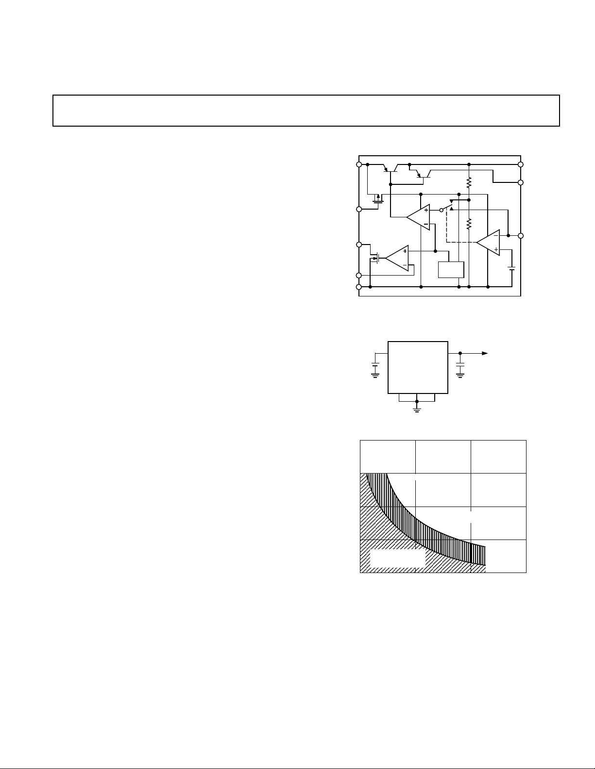
FUNCTIONAL BLOCK DIAGRAM
TYPICAL OPERATING CIRCUIT
+6V
INPUT
IN
+
ADP3367
OUT
+
C1
10µF
+5V
OUTPUT
GENERAL DESCRIPTION
GNDSET SHDN
The ADP3367 is a low-dropout precision voltage regulator that
can supply up to 300 mA output current. It can be used to give
a fixed +5 V output with no additional external components or
can be adjusted from +1.3 V to +16 V using two external
resistors. Fixed or adjustable operation can be selected via the
SET input. The low quiescent current (17 µA) in conjunction
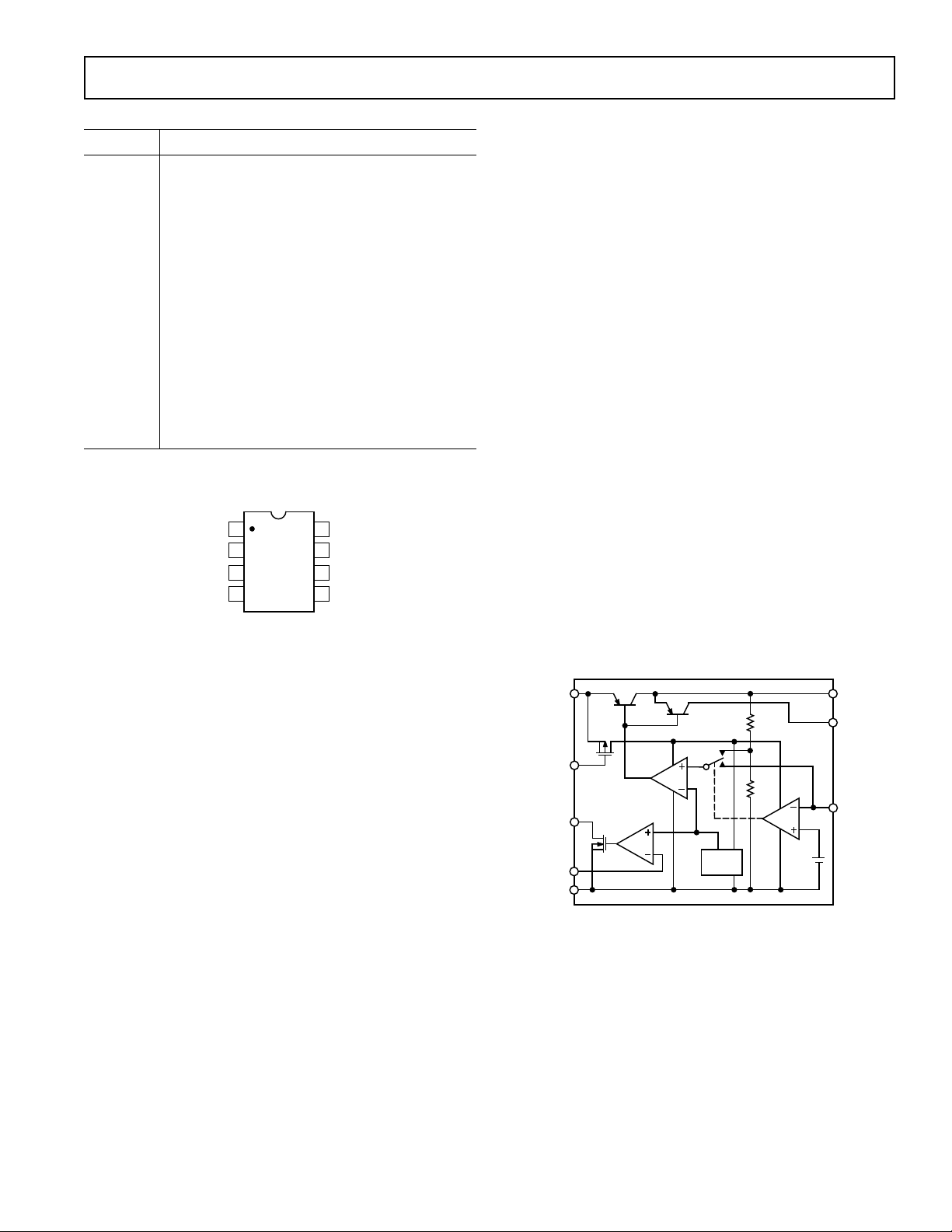
400
TA = +50°C
with the standby or shutdown mode (0.2 µA) makes this device
especially suitable for battery powered systems. The dropout
voltage when supplying 100 µA is only 15 mV allowing opera-
300
GUARANTEED 300mA
tion with minimal headroom thereby prolonging the useful battery life. At higher output current levels the dropout remains
low increasing to just 150 mV when supplying 200 mA. A wide
input voltage range from 2.5 V to 16.5 V is allowable. Additional features include a dropout detector and a low supply/battery monitoring comparator. The dropout detector can be used
to signal loss of regulation while the low battery detector can be
used to monitor the input supply voltage.
The ADP3367 is a much improved pin-compatible replacement
for the MAX667. Improvements include lower supply current,
tighter voltage accuracy and superior line and load regulation.
Improved ESD protection (>6000 V) is achieved by advanced
voltage clamping structures. The ADP3367 is specified over the
industrial temperature range –40°C to +85°C and is available in
narrow surface mount (SOIC) packages.
ADI’s proprietary Thermal Coastline leadframe used in ADP3367AR
packaging, has 30% lower thermal resistance than the standard
leadframes. This improvement in heat flow rate results in lower
200
LOAD CURRENT – mA
100
STANDARD
SO PACKAGE
DISSIPATION LIMIT
0
015
ADP3367
DISSIPATION LIMIT
510
VIN–V
– V
OUT
Load Current vs. Input-Output Differential Voltage
die temperature hence improves reliability.
*Patent pending.
REV. 0
Information furnished by Analog Devices is believed to be accurate and
reliable. However, no responsibility is assumed by Analog Devices for its
use, nor for any infringements of patents or other rights of third parties
which may result from its use. No license is granted by implication or
otherwise under any patent or patent rights of Analog Devices.
One Technology Way, P.O. Box 9106, Norwood, MA 02062-9106, U.S.A.
Tel: 617/329-4700 Fax: 617/326-8703
© Analog Devices, Inc., 1995
Page 2
ADP3367–SPECIFICA TIONS
(VIN = +9 V, GND = 0 V, V
= +5 V, TA = T
OUT
MIN
to T
unless otherwise noted)
MAX
Parameter Min Typ Max Units Test Conditions/Comments
Input Voltage, V
IN
Output Voltage, V
OUT
2.5 16.5 V
4.9 5.0 5.1 V V
= 0 V, VIN = 6 V, I
SET
Maximum Output Current 200 mA VIN = +9 V, + 4.5 V < V
Quiescent Current
: Shutdown Mode 0.2 0.75 µAV
I
GND
: Normal Mode V
I
GND
17 25 µAI
20 30 µAI
514 mAI
= 2 V
SHDN
= 0 V, V
SHDN
= 0 µA
OUT
= 100 µA
OUT
= 200 mA
OUT
SET
= 0 V
Dropout Voltage
= 5 V 15 40 mV I
V
OUT
60 125 mV I
100 175 mV I
150 250 mV I
175 300 mV I
300 500 mV I
= 3.3 V 94 140 mV I
V
OUT
210 312 mV I
430 625 mV I
Load Regulation 5 10 mV I
Line Regulation 0.1 5 mV VIN = 6 V to 10 V, I
Reference Voltage, V
SET
1.23 1.255 1.28 V
= 100 µA
OUT
= 50 mA
OUT
= 100 mA
OUT
= 200 mA, TA = +25°C
OUT
= 200 mA
OUT
= 300 mA
OUT
= 50 mA
OUT
= 100 mA
OUT
= 200 mA, TA = +25°C
OUT
= 10 mA–100 mA, VIN = 6 V
OUT
= 10 mA–200 mA, VIN = 6 V
I
OUT
OUT
= 10 mA
SET Input Threshold 50 mV
SET Input Current, I
Output Leakage Current, I
Short Circuit Current, I
Low Battery Detector Input Threshold, V
SET
OUT
OUT
LBI
1.215 1.255 1.295 V
±0.01 ±10 nA V
0.1 1 µAV
= 1.5 V
SET
SHDN
= 2 V
400 mA TA = +25°C
450 mA TA = T
MIN
to T
MAX
LBI Hysteresis 6 mV
LBI Input Leakage Current, I
Low Battery Detector Output Voltage, V
LBI
LBO
±0.01 ±10 nA V
0.25 V V
0.40 V V
Shutdown Input Voltage, V
SHDN
1.5 V V
0.4 V V
Shutdown Input Current, I
SHDN
±0.01 ±10 nA V
Dropout Detector Output Voltage 0.25 V (V
4.0 (V
Specifications subject to change without notice.
= 1.5 V
LBI
= 0 V, I
LBI
= 0 V, I
LBI
IH
IL
= 0 V to V
SHDN
= 0 V, V
SET
= 7 V, I
V
IN
SET
OUT
= 0 V, V
VIN = 4.5 V, I
= 10 mA, TA = +25°C
LBO
= 10 mA, TA = T
LBO
IN
= 0 V, RDD = 100 kΩ,
SHDN
= 10 mA)
= 0 V, RDD = 100 kΩ,
SHDN
= 10 mA)
OUT
= 10 mA
OUT
< +5.5 V
OUT
MIN
to T
MAX
ABSOLUTE MAXIMUM RATINGS*
(
TA= +25°C unless otherwise noted)
Input Voltage, VIN . . . . . . . . . . . . . . . . . . . . . . . . . . . . . +18 V
Output Short Circuit to GND Duration . . . . . . . . . . . . . 1 sec
LBO Output Sink Current . . . . . . . . . . . . . . . . . . . . . . . 50 mA
LBO Output Voltage . . . . . . . . . . . . . . . . . . . . . GND to V
OUT
SHDN Input Voltage . . . . . . . . . . . . . . –0.3 V to (VIN + 0.3 V)
LBI, SET Input Voltage . . . . . . . . . . . –0.3 V to (V
+ 0.3 V)
IN
Power Dissipation, R-8 . . . . . . . . . . . . . . . . . . . . . . . 960 mW
(Derate 10 mW/°C above +50°C)
θ
, Thermal Impedance . . . . . . . . . . . . . . . . . . . . . . 98°C/W
JA
Operating Temperature Range
Industrial (A Version) . . . . . . . . . . . . . . . . . –40°C to +85°C
Storage Temperature Range . . . . . . . . . . . –65°C to +150°C
Lead Temperature (Soldering, 10 sec) . . . . . . . . . . . . . +300°C
Vapor Phase (60 sec) . . . . . . . . . . . . . . . . . . . . . . . . +215°C
Infrared (15 sec) . . . . . . . . . . . . . . . . . . . . . . . . . . . . +220°C
ESD Rating . . . . . . . . . . . . . . . . . . . . . . . . . . . . . . . . > 6000 V
*This is a stress rating only and functional operation of the device at these or any
other conditions above those indicated in the operation sections of this specification is not implied. Exposure to absolute maximum rating conditions for extended
periods of time may affect reliability.
ORDERING GUIDE
Model Temperature Range Package Option*
ADP3367AR –40°C to +85°C SO-8
*SO = Small Outline Package.
–2–
REV. 0
Page 3
ADP3367
ADP3367
IN
SHDN
LBO
LBI
GND
50mV
SET
DD
OUT
1.255V
REF
A1
C1
C2
PIN FUNCTION DESCRIPTION
Mnemonic Function
DD Dropout Detector Output. PNP collector output
GENERAL INFORMATION
The ADP3367 contains a micropower bandgap reference voltage source, an error amplifier A1, two comparators (C1, C2)
and a series PNP output pass transistor.
which sources current as dropout is reached.
V
IN
Voltage Regulator Input.
GND Ground Pin. Must be connected to 0 V.
LBI Low Battery Detect Input. Compared with 1.255 V.
LBO Low Battery Detect Output. Open Drain Output
that goes low when LBI is below the threshold.
SHDN Digital Input. May be used to disable the device
so that the power consumption is minimized.
SET Voltage Setting Input. Connect to GND for +5 V
output or connect to resistive divider for adjust-
able output.
OUT Regulated Output Voltage. Connect to filter
capacitor.
CIRCUIT DESCRIPTION
The internal bandgap voltage reference is trimmed to 1.255V
and is used as a reference input to the error amplifier A1. The
feedback signal from the regulator output is supplied to the
other input by an on-chip voltage divider or by two external
resistors. When the SET input is at ground, the internal divider
provides the error amplifier’s feedback signal giving a +5V output. When SET is at more than 50 mV above ground, comparator C1 switches the error amplifier’s input directly to the SET
pin, and external resistors are used to set the output voltage.
The external resistors are selected so that the desired output
voltage gives 1.255 V at the SET input.
The output from the error amplifier supplies base current to the
PNP output pass transistor which provides output current. Up
to 300 mA output current is available provided that the device
power dissipation is not exceeded.
DIP & SOIC PIN CONFIGURATION
Comparator C2 compares the voltage on the Low Battery Input
(LBI) pin to the internal +1.255 V reference voltage. The out-
DD
OUT
LBI
GND
1
2
ADP3367
TOP VIEW
3
(Not to Scale)
4
8
IN
7
LBO
6
SET
5
SHDN
put from the comparator drives an open drain FET connected
to the Low Battery Output pin, LBO. The Low Battery Threshold may be set using a suitable voltage divider connected to
LBI. When the voltage on LBI falls below 1.255 V, the open
drain output, LBO, is pulled low.
A shutdown (SHDN) input that can be used to disable the
error amplifier and hence the voltage output is also available.
TERMINOLOGY
The supply current in shutdown is less than 0.75 µA.
Dropout Voltage: The input/output voltage differential at
which the regulator no longer maintains regulation against further reductions in input voltage. It is measured when the output
decreases 100 mV from its nominal value. The nominal value is
the measured value with V
IN
= V
OUT
+2 V.
Line Regulation: The change in output voltage as a result of a
change in the input voltage. It is specified for a change of input
voltage from 6 V to 10 V.
Load Regulation: The change in output voltage for a change
in output current. It is specified for an output current change
from 10 mA to 200 mA.
Quiescent Current (I
): The input bias current which
GND
flows into the regulator not including load current. It is measured on the GND line and is specified in shutdown and also for
different values of load current.
Figure 1. ADP3367 Functional Block Diagram
Shutdown: The regulator is disabled and power consumption
is minimized.
Dropout Detector: An output that indicates that the regulator
is dropping out of regulation.
Maximum Power Dissipation: The maximum total device
dissipation for which the regulator will continue to operate
within specifications.
REV. 0
–3–
Page 4

CH1 2.00V CH2 200mV M 2.00ms
TA = +25°C
+10V
+6V
V
IN
V
OUT
200mV
0V
ADP3367–T ypical Performance Characteristics
500
TA = +25°C
250
DROPOUT VOLTAGE – mV
10
1
LOAD CURRENT – mA
Figure 2. Dropout Voltage vs. Load Current
10
V
= 6V
IN
= +25°C
T
A
1
2.5
TA = +25°C
V
= 6V
IN
= 10µF
C
L
2.0
1.5
∆V – mV
1.0
0.5
300100 200
0.0
0 200
Figure 5. Load Regulation (DV
50 100 150
∆1 – mA
OUT
vs. DI
OUT
)
0.1
GROUND CURRENT – mA
0.01
0.01
I
OUT
– mA
100101
Figure 3. Ground Current vs. Load Current
1000
TA = +25°CTA = +25°C
100mA
100
20mA
10mA
10
DD OUTPUT CURRENT – µA
1
0.00 0.450.05
5mA
2mA
0.10 0.15 0.20 0.25 0.30 0.35 0.40
50mA
I-O DIFFERENCE – mV
10000.1
Figure 6. Dynamic Response to Input Change
OUTPUT
CURRENT
V
OUT
CH1 1.00V CH2 20.0mV M 2.00ms
100mA
10mA
20mV
0V
Figure 4. DD Output Current vs. I-O Differential
–4–
Figure 7. Dynamic Response to Load Change
REV. 0
Page 5

ADP3367
IN
OUT
LBO
ADP3367
C1
10µF
+
10kΩ
V
IN
LBI
GND SETSHDN
R3
R4
LOW BATTERY
STATUS OUTPUT
V
OUT
APPLICATIONS INFORMATION
Circuit Configurations
For a fixed +5 V output the SET input should be grounded, and
no external resistors are necessary. This basic configuration is
shown in Figure 8. The input voltage can range from +5.15 V
to +16.5 V, and output currents up to 300 mA are available
provided that the maximum package power dissipation is not
exceeded.
IN
++
ADP3367
OUT
GNDSET SHDN
C1
10µF
+5V
OUTPUT
Figure 8. Fixed +5 V Output Circuit
Output Voltage Setting
If the SET input is connected to a resistor divider network, the
output voltage is set according to the following equation:
R1+ R2
×
R1
where V
= 1.255 V.
SET
V
OUT=VSET
Low Supply or Low Battery Detection
The ADP3367 contains on-chip circuitry for low power supply
or battery detection. If the voltage on the LBI pin falls below
the internal 1.255 V reference, then the open drain output LBO
will go low. The low threshold voltage may be set to any voltage
above 1.255 V by appropriate resistor divider selection.
V
R3= R4×
BATT
V
where R3 and R4 are the resistive divider resistors and V
LBI
−1
is
BATT
the desired low voltage threshold.
Since the LBI input leakage current is less than 10 nA, large
values may be selected for R3 and R4 in order to minimize
loading. For example, a 6 V low threshold, may be set using
10 MΩ for R3 and 2.7 MΩ for R4.
The LBO output is an open-drain output that goes low sinking
current when LBI is less than 1.255 V. A pull-up resistor of
10 kΩ or greater may be used to obtain a logic output level with
the pull-up resistor connected to V
OUT
.
V
IN
IN
ADP3367
SHDN
GND
OUT
SET
V
C1
10µF
OUT
Figure 10. Low Battery/Supply Detect Circuit
Dropout Detector
+
R2
R1
The ADP3367 features an extremely low dropout voltage making it suitable for low voltage systems where headroom is
limited. A dropout detector is also provided. The dropout
Figure 9. Adjustable Output Circuit
The resistor values may be selected by first choosing a value for
R1 and then selecting R2 according to the following equation:
R2 = R1×
V
OUT
V
SET
−1
The input leakage current on SET is 10 nA maximum. This
allows large resistor values to be chosen for R1 and R2 with
little degradation in accuracy. For example, a 1 MΩ resistor
may be selected for R1, and then R2 may be calculated accordingly. The tolerance on SET is guaranteed at less than ± 25 mV,
so in most applications fixed resistors will be suitable.
Shutdown Input (SHDN)
detector output, DD, changes as the dropout voltage approaches
its limit. This is useful for warning that regulation can no longer be
maintained. The dropout detector output is an open collector output from a PNP transistor. Under normal operating conditions
with the input voltage more than 300mV above the output, the
PNP transistor is off and no current flows out the DD pin. As the
voltage differential reduces to less than 300mV, the transistor
switches on and current is sourced. This condition indicates that
regulation can no longer be maintained. Please refer to Figure 4 in
the “Typical Performance Characteristics.” The current output
can be translated into a voltage output by connecting a resistor
from DD to GND. A resistor value of 100 kΩ is suitable. A digital
status signal can be obtained using a comparator. The on-chip
comparator LBI may be used if it is not being used to monitor a
battery voltage. This is illustrated in Figure 11.
The SHDN input allows the regulator to be switched off with a
logic level signal. This will disable the output and reduce the
current drain to a low quiescent (0.75 µA maximum) current.
This is very useful for low power applications. Driving the
SHDN input to greater than 1.5 V places the part in shutdown.
If the shutdown function is not being used, then SHDN should
be connected to GND.
REV. 0
–5–
Page 6

ADP3367
+
C1
10µF
IN OUT
ADP3367
+5V
OUTPUT
GND
SET
SHDN
DD
R1
610kΩ
R2
2MΩ
R3
1MΩ
+
V
IN
QUIESCENT CURRENT BELOW DROPOUT
0
1623 5
400
200
900
1mA
800
700
600
500µA
300
100
4
1.2mA
900µA
V
IN
– V
GROUND PIN CURRENT
IN
+
V
IN
ADP3367
LBI
GNDSET SHDN
Figure 11. Dropout Status Output
Output Capacitor
An output capacitor is required on the ADP3367 to maintain stability and also to improve the load transient response. Capacitor
values from 10 µF upwards are recommended. Capacitors larger
than 10 µF will further improve the transient response. Tantalum
or aluminum electrolytics are suitable for most applications. For
temperatures below about –25°C, solid tantalums should be used
as many aluminum electrolytes freeze at this temperature.
Quiescent Current Considerations
The ADP3367 uses a PNP output stage to achieve low dropout
voltages combined with high output current capability. Under
normal regulating conditions the quiescent current is extremely
low. However if the input voltage drops so that it is below the
desired output voltage, the quiescent current increases considerably. This happens because regulation can no longer be maintained and large base current flows in the PNP output transistor
in an attempt to hold it fully on. For minimum quiescent current, it is therefore important that the input voltage is maintained higher than the desired output level. If the device is being
powered using a battery that can discharge down below the recommended level, there are a couple of techniques that can be
applied to reduce the quiescent current, but at the expense of
dropout voltage. The first of these is illustrated in Figure 12. By
connecting DD to SHDN the regulator is partially disabled with
input voltages below the desired output voltage and therefore
the quiescent current is reduced considerably.
IN OUT
+
V
IN
Another technique for reducing the quiescent current near dropout is illustrated in Figure 13. The DD output is used to modify
the output voltage so that as V
age setpoint also drops. This technique only works when external resistors are used to set the output voltage. With V
than V
, DD has no effect. As VINreduces and dropout is
OUT
ADP3367
Figure 12. IQ Reduction 1
OUT
+
C1
10µF
LBO
DD
R1
100kΩ
+
C1
10µF
DD
GNDSET SHDN
R1
47kΩ
drops, the desired output volt-
IN
R2
10kΩ
DROPOUT
STATUS
OUTPUT
+5V
OUTPUT
C2
0.1µF
+5V
OUTPUT
IN
greater
reached, the DD output starts sourcing current into the SET
input through R3. This increases the SET voltage so that the
regulator feedback loop does not drive the internal PNP transistor as hard as it otherwise would. As the input voltage continues
to decrease, more current is sourced, thereby reducing the PNP
drive even further. The advantage of this scheme is that it maintains a low quiescent current down to very low values of V
IN
which point the batteries are well outside their useful operating
range. The output voltage tracks the input voltage minus the
dropout. The SHDN function is also unaffected and may be
used normally if desired.
Figure 13. IQ Reduction 2
POWER DISSIPATION
The ADP3367 can supply currents up to 300mA and can operate with input voltages as high as 16.5 V, but not simultaneously.
It is important that the power dissipation and hence the internal
die temperature be maintained below the maximum limits. Power
Dissipation is the product of the voltage differential across the
regulator times the current being supplied to the load. The
maximum package power dissipation is given in the Absolute
Maximum Ratings. In order to avoid excessive die temperatures,
these ratings must be strictly observed.
P
= (VIN– V
D
OUT
) (IL)
The die temperature is dependent on both the ambient temperature and on the power being dissipated by the device. The internal die temperature must not exceed 125°C. Therefore, care
must be taken to ensure that, under normal operating conditions, the die temperature is kept below the thermal limit.
T
–6–
= TA + PD (
J
θ
)
JA
REV. 0
at
Page 7

ADP3367
This may be expressed in terms of power dissipation as follows:
= (TJ– TA)/(
P
D
θ
)
JA
where:
= Die Junction Temperature (°C)
T
J
= Ambient Temperature (°C)
T
A
= Power Dissipation (W)
P
D
θ
= Junction to Ambient Thermal Resistance (°C/W)
JA
If the device is being operated at the maximum permitted ambient temperature of 85°C, the maximum power dissipation permitted is:
P
(max) = (TJ (max) – TA)/(
D
(max) = (125 – 85)/(θJA)
P
D
θ
= 40/
JA
θ
)
JA
where:
θ
= 98°C/W for the 8-pin SOIC (R-8) package
JA
Therefore, for a maximum ambient temperature of 85°C
(max) = 408 mW for R-8
P
D
At lower ambient temperatures the maximum permitted power
dissipation increases accordingly up to the maximum limits
specified in the absolute maximum specifications.
The thermal impedance (θ
) figures given are measured in still
JA
air conditions and are reduced considerably where fan assisted
cooling is employed. Other techniques for reducing the thermal
impedance include large contact pads on the printed circuit
board and wide traces. The copper will act as a heat exchanger
thereby reducing the effective thermal impedance.
POWER DISSIPATION
Low Thermal Resistance Package
The ADP3367 utilizes a patented and proprietary Thermal
Coastline Leadframe which offers significantly lower resistance
to heat flow from die to the PC board.
Heat generated on the die is removed and transferred to the PC
board faster resulting in lower die temperature than standard
packages. Table II is a performance comparison between and
standard and Thermal Coastline package.
Table I. Thermal Resistance Performance Comparison*
Standard Package (SO-8) Thermal Coastline Package
44°C/W 40°C/W
θ
JC
θ
170°C/W 98°C/W
JA
PD 235 mW 408 mW
*Data presented in Table II is obtained using SEMI Standard Method G38-47
and SEMI Standard Specification G42-88.
A device operating at room temperature, +25°C, and +125°C
junction temperature can dissipate 1.15 W.
To maintain this high level of heat removal efficiency, once heat
is removed from the die to the PC board, it should be dissipated
to the air or other mediums to maintain the largest possible tem-
perature differential between the die and PC board; remember,
the rate at which heat is transferred is directly proportional to
the temperature differential.
Various PC board layout techniques could be used to remove
the heat from the immediate vicinity of the package. Consider
the following issues when designing a board layout:
1. PC board traces with larger copper cross section areas will
remove more heat; use PCs with thicker copper and/or wider
traces.
2. Increase the surface area exposed to open air so heat can be
removed by convection or forced air flow.
3. Use larger masses such as heat sinks or thermally conductive
enclosures to distribute and dissipate the heat.
4. Do not solder mask or silk screen the heat dissipating traces;
black anodizing will significantly improve heat dissipation by
means of increased radiation.
High Power Dissipation Recommendations
Where excessive power dissipation due to high input-output
differential voltages and/or high current conditions exists, the
simplest method of reducing the power requirements on the
regulator is to use a series dropper resistor. In this way the
excess power can be dissipated in the external resistor. As an
example, consider an input voltage of +12V and an output
voltage requirement of +5 V @ 100 mA with an ambient temperature of +85°C. The package power dissipation under these
conditions is 700 mW which exceeds the maximum ratings. By
using a dropper resistor to drop 4 V, the power dissipation
requirement for the regulator is reduced to 300 mW which is
within the maximum specifications for the SO-8 package at
85°C. The resistor value is calculated as R = 4/0.1 = 40Ω.A
resistor power rating of 1/2 W or greater may be used.
40Ω
0.5W
V
12V
IN
1µF
IN
+
C1
ADP3367
OUT
GNDSET SHDN
+
C2
10µF
+5V
OUTPUT
Figure 14. Reducing Regulator Power Dissipation
Transient Response
The ADP3367 exhibits excellent transient performance as illustrated in the “Typical Performance Characteristics.” Figure 6
shows that an input step from 10 V to 6V results in a very small
output disturbance (50 mV). Adding an input capacitor would
improve this even more.
Figure 7 shows how quickly the regulator recovers from an output load change from 10 mA to 100mA. The offset due to the
load current change is less than 1 mV.
Monitored µP Power Supply
Figure 15 shows the ADP3367 being used in a monitored µP
supply application. The ADP3367 supplies +5V for the micro-
REV. 0
–7–
Page 8

ADP3367
IN
OUT
GND SET SHDN
ADP3367
10µF
+
+5V
ADM705
RESET
PFO
GND
PFI
UNREGULATED
DC
R1
R2
V
CC
µP
RESET
INTERRUPT
V
CC
processor. Monitoring the supply, the ADM705 will generate a
reset if the supply voltage falls below 4.65 V. Early warning of
an impending power fail is generated by a power fail comparator
on the ADM705. A resistive divider network samples the preregulator input voltage so that failing power is detected while
the regulator is still operating normally. An interrupt is generated so that a power-down sequence can be completed before
power is completely lost. The low dropout voltage on the
ADP3367 maximizes the available time to carry out the powerdown sequence. The resistor divider network R1 and R2 should
be selected so that the voltage on PFI is 1.25V at the desired
warning voltage.
OUTLINE DIMENSIONS
Dimensions shown in inches and (mm).
C2083–10–10/95
Figure 15.µP Regulator with Supply Monitoring and Early
Power-Fail Warning
0.0098 (0.25)
0.0040 (0.10)
8-Lead Narrow-Body SOIC
(SO-8)
PIN 1
8
1
0.1968 (5.00)
0.1890 (4.80)
0.0500
(1.27)
BSC
5
4
0.0192 (0.49)
0.0138 (0.35)
0.1574 (4.00)
0.1497 (3.80)
0.2440 (6.20)
0.2284 (5.80)
0.0688 (1.75)
0.0532 (1.35)
0.0098 (0.25)
0.0075 (0.19)
8
°
0
°
0.0196 (0.50)
0.0099 (0.25)
0.0500 (1.27)
0.0160 (0.41)
x 45
°
PRINTED IN U.S.A.
–8–
REV. 0
 Loading...