

Page 1
High Accuracy anyCAP™ Adjustable
ADP3303A
ERR
OUT
IN
FB
R1
C2
1mF
V
OUT
= +5V
ON
OFF
SD
GND
C1
0.47mF
V
IN
R2
R3
330kV
E
OUT
SD
a
FEATURES
High Accuracy Over Line and Load:
ⴞ0.8% @ +25ⴗC, ⴞ1.4% Over Temperature
Ultralow Dropout Voltage: 150 mV Typical @ 200 mA
Requires Only C
anyCAP = Stable with All Types of Capacitors
(Including MLCC)
Current and Thermal Limiting
Low Noise
Dropout Detector
Low Shutdown Current: 1 A
3.2 V to 12 V Supply Range
Adjustable 2.2 V to 10 V Output Range
–20ⴗC to +85ⴗC Ambient Temperature Range
Thermally Enhanced TSSOP-14 Package
APPLICATIONS
Cellular Telephones
Notebook, Palmtop Computers
Battery Powered Systems
Portable Instruments
Post Regulator for Switching Supplies
Bar Code Scanners
= 1 F for Stability
O
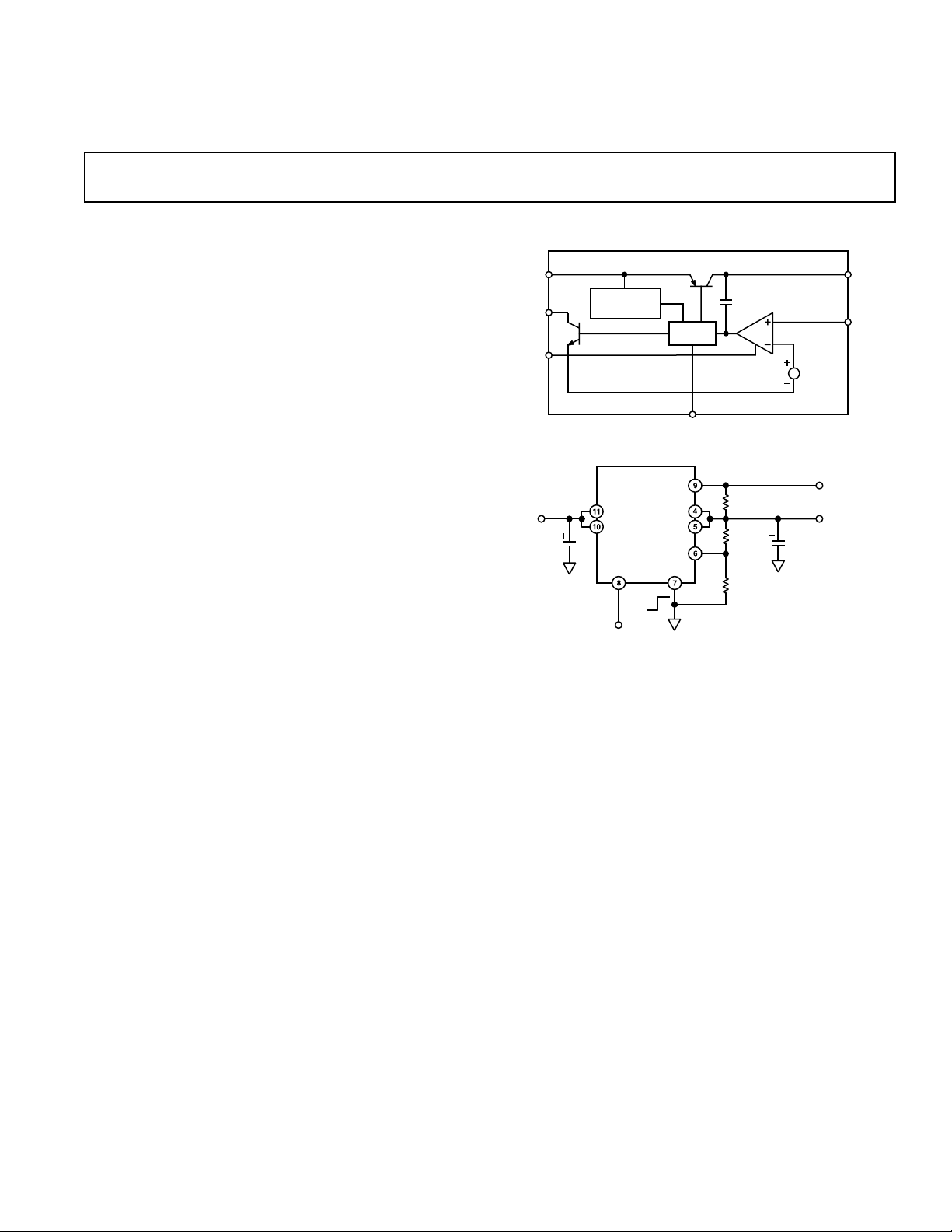
200 mA Low Dropout Linear Regulator
ADP3303A
FUNCTIONAL BLOCK DIAGRAM
ADP3303A
CC
g
m
BANDGAP
REF
OUT
FB
ERR
SD
IN
THERMAL
PROTECTION
Q2
Q1
DRIVER
GND
Figure 1. Typical Application Circuit
GENERAL DESCRIPTION
The ADP3303A is a member of the ADP330x family of precision low dropout anyCAP voltage regulators. The ADP3303A
stands out from conventional LDOs with a novel architecture,
an enhanced process and a new package. Its patented design
requires only a 1 µF output capacitor for stability. This device is
insensitive to output capacitor ESR (Equivalent Series Resistance), and is stable with any good quality capacitor, including
ceramic types (MLCC) for space restricted applications. The
ADP3303A achieves exceptional accuracy of ±0.8% at room
temperature and ±1.4% overall accuracy over temperature, line
and load variations. The dropout voltage of the ADP3303A is
only 150 mV (typical) at 200 mA.
anyCAP is a trademark of Analog Devices Inc.
REV. A
Information furnished by Analog Devices is believed to be accurate and
reliable. However, no responsibility is assumed by Analog Devices for its
use, nor for any infringements of patents or other rights of third parties
which may result from its use. No license is granted by implication or
otherwise under any patent or patent rights of Analog Devices.
In addition to the new architecture and process, ADI’s new
proprietary thermally enhanced package (Thermal Coastline)
can handle 1 W of power dissipation without an external heat
sink or large copper surface on the PC board. This keeps PC
board real estate to a minimum and makes the ADP3303A very
attractive for use in portable equipment.
The ADP3303A operates over an input voltage range of 3.2 V
to 12 V and delivers a load current in excess of 200 mA. The
output voltage can be adjusted from 2.2 V to 10 V using an
external resistor divider. It also features an error flag that signals
when the device is about to lose regulation or when the short
circuit or thermal overload protection is activated. Other features include shutdown and optional noise reduction capabilities.
One Technology Way, P.O. Box 9106, Norwood, MA 02062-9106, U.S.A.
Tel: 781/329-4700 World Wide Web Site: http://www.analog.com
Fax: 781/326-8703 © Analog Devices, Inc., 1999
Page 2

ADP3303A–SPECIFICATIONS
(@ TA = –20ⴗC to +85ⴗC, VIN = 7 V, CIN = 0.47 F, C
1
noted)
= 1 F, unless otherwise
OUT
Parameter Symbol Conditions Min Typ Max Units
OUTPUT VOLTAGE
ACCURACY I
2, 3, 4
V
OUT
VIN = Nom V
= 1.0 mA to 200 mA
L
T
= +25°C –0.8 +0.8 %
A
V
= Nom V
IN
+0.5 V to +12 V
OUT
+0.5 V to +12 V
OUT
IL = 1.0 mA to 200 mA –1.4 +1.4 %
LINE REGULATION ∆V
∆V
LOAD REGULATION ∆V
∆I
GROUND CURRENT
5
I
GND
O
IN
O
L
VIN = Nom V
T
= +25°C 0.01 mV/V
A
+0.5 V to +12 V
OUT
IL = 1.0 mA to 200 mA
T
= +25°C 0.005 mV/mA
A
IL = 200 mA 2.0 4 mA
IL = 1.0 mA 0.35 0.6 mA
GROUND CURRENT
5
I
GND
VIN = 2.5 V, V
OUT
= 5.0 V
IN DROPOUT IL = 1.0 mA 1.9 3.0 mA
V
DROPOUT VOLTAGE V
DROP
≤ 98% of VO Nominal
OUT
I
= 200 mA 0.15 0.4 V
L
I
= 10 mA 0.02 0.07 V
L
IL = 1 mA 0.003 0.03 V
SHUTDOWN THRESHOLD V
THSD
ON 2.0 0.9 V
OFF 0.9 0.3 V
SHUTDOWN PIN I
SDIN
0 V < VSD
≤
5 V 1 µA
INPUT CURRENT 5 V ≤ VSD ≤ 12 V @ VIN = 12 V 22 µA
GROUND CURRENT IN
5
SHUTDOWN MODE T
OUTPUT CURRENT IN I
SHUTDOWN MODE T
I
Q
OSD
VSD = 0, VIN = 12 V
= +25°C1µA
A
V
= 0 V, VIN = 12 V
SD
T
= +85°C5µA
A
T
= +25°C @ VIN = 12 V 2.5 µA
A
= +85°C @ VIN = 12 V 4 µA
A
ERROR PIN OUTPUT
LEAKAGE I
EL
V
= 5 V 13 µA
EO
ERROR PIN OUTPUT
“LOW” VOLTAGE V
PEAK LOAD CURRENT I
OUTPUT NOISE V
EOL
LDPK
NOISE
@ 5 V OUTPUT C
NOTES
1
Ambient temperature of +85°C corresponds to a typical junction temperature of +125°C under typical full load test conditions. The formula for Nom V
in the Output Voltage Selection section.
2
Accuracy guaranteed using external trim pots.
3
For 2.7 V output, the minimum VIN is 3.2 V.
4
Guaranteed by design and characterization.
5
Ground currents include the current through R1, R2.
Specifications subject to change without notice.
I
= 400 µA 0.15 0.3 V
SINK
VIN = Nom V
+ 1 V 300 mA
OUT
f = 10 Hz–100 kHz
= 0 100 µV
NR
CNR = 10 nF, C
= 10 µF30µV
L
OUT
rms
rms
is found
–2–
REV. A
Page 3
ADP3303A
WARNING!
ESD SENSITIVE DEVICE
ABSOLUTE MAXIMUM RATINGS*
Input Supply Voltage . . . . . . . . . . . . . . . . . . . –0.3 V to +16 V
Shutdown Input Voltage . . . . . . . . . . . . . . . . –0.3 V to +16 V
Error Flag Output Voltage . . . . . . . . . . . . . . . –0.3 V to +16 V
Noise Bypass Pin Voltage . . . . . . . . . . . . . . . . –0.3 V to +5 V
Power Dissipation . . . . . . . . . . . . . . . . . . . Internally Limited
Operating Ambient Temperature Range . . . –55°C to +125°C
Operation Junction Temperature Range . . . –55°C to +125°C
. . . . . . . . . . . . . . . . . . . . . . . . . . . . . . . . . . . . . 96°C/W
θ
JA
Storage Temperature Range . . . . . . . . . . . . –65°C to +150°C
Lead Temperature Range (Soldering 10 sec) . . . . . . . +300°C
Vapor Phase (60 sec) . . . . . . . . . . . . . . . . . . . . . . . +215°C
Infrared (15 sec) . . . . . . . . . . . . . . . . . . . . . . . . . . +220°C
*This is a stress rating only; operation beyond these limits can cause the device to
be permanently damaged.
Other Members of anyCAP Family
Output Package
Model Current Options
2
1
Comments
ADP3300 50 mA SOT-23-6 High Accuracy
ADP3301 100 mA SO-8 High Accuracy
ADP3302 100 mA SO-8 Dual Output
ADP3307 100 mA SOT-23-6 High Accuracy
ADP3308 50 mA SOT-23-5 High Accuracy
ADP3309 100 mA SOT-23-5 High Accuracy
NOTES
1
See individual data sheets for detailed ordering information.
2
SO = Small Outline, SOT = Surface Mount Outline.
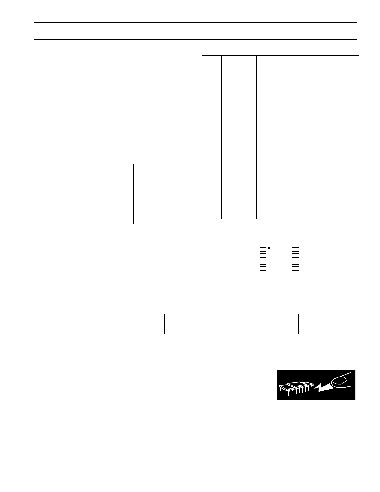
PIN FUNCTION DESCRIPTIONS
Pin Mnemonic Function
1–3 NC No Connect.
4 & 5 OUT Output of the Regulator. Bypass to
ground with a 1 µF or larger capacitor.
Pins 4 and 5 must be connected
together for proper operation.
6 FB Feedback. Connect to an external
resistor divider that sets the output
voltage.
7 GND Ground.
8 SD Active Low Shutdown Pin. Connect to
ground to disable the regulator output.
When shutdown is not used, this pin
should be connected to the input pin.
9 ERR Open Collector Output that goes low to
indicate that the output is about to go
out of regulation.
10 & 11 IN Regulator Input. Pins 10 and 11 must
be connected together for proper
operation.
12–14 NC No Connect.
PIN CONFIGURATION
NC
NC
NC
OUT
OUT
FB
GND
NC = NO CONNECT
ADP3303A
TOP VIEW
(Not to Scale)
NC
NC
NC
IN
IN
ERR
SD
ORDERING GUIDE
Model Voltage Output Package Description Package Option
ADP3303AARU-Reel ADJ Thin Shrink Small Outline Package (TSSOP) TSSOP-14
NOTES
All devices operate over the ambient temperature range of –20°C to +85°C.
Contact the factory for the availability of other output voltage options.
CAUTION
ESD (electrostatic discharge) sensitive device. Electrostatic charges as high as 4000 V readily
accumulate on the human body and test equipment and can discharge without detection.
Although the ADP3303A features proprietary ESD protection circuitry, permanent damage may
occur on devices subjected to high energy electrostatic discharges. Therefore, proper ESD
precautions are recommended to avoid performance degradation or loss of functionality.
REV. A
–3–
Page 4

ADP3303A
–Typical Performance Characteristics
3.30025
3.30000
3.29975
3.29950
3.29925
3.29900
OUTPUT VOLTAGE – Volts
3.29875
3.29850
3.5 4 165 6 7 8 9 10 1112131415
IL = 0mA
IL = 10mA
V
OUT
IL = 100mA
IL = 200mA
INPUT VOLTAGE – Volts
= +3.3V
Figure 2. Line Regulation: Output
Voltage vs. Supply Voltage
2000
1800
1600
1400
1200
1000
800
600
GROUND CURRENT – mA
400
200
40 60 80 100 120 140 160 180
0 20 200
IL = 0 TO 200mA
OUTPUT LOAD – mA
3.30025
3.30000
3.29975
3.29950
3.29925
OUTPUT VOLTAGE – Volts
3.29900
3.29875
40 60 80 100 120 140 160180
0 20 200
OUTPUT LOAD – mA
VIN = +7V
= +3.3V
V
OUT
Figure 3. Output Voltage vs. Load
Current
0.2
0.1
0.0
–0.1
–0.2
OUTPUT VOLTAGE – %
–0.3
–0.4
–45 –25 135
IL = 0mA
–5 15 35 75 95 11555
TEMPERATURE – C
V
2.0
1.6
1.2
0.8
GROUND CURRENT – mA
0.4
0
02
468 12141610
INPUT VOLTAGE – Volts
OUT
I
L
Figure 4. Quiescent Current vs.
Supply Voltage
3000
2500
2000
1500
1000
\
GROUND CURRENT – mA
500
0
–25 –5 135
IL = 200mA
IL = 100mA
IL = 0mA
15 35 55 75 95 115
TEMPERATURE – C
= +3.3V
= 0mA
VIN = +7V
Figure 5. Quiescent Current vs. Load
Current
180
160
140
120
100
80
60
40
INPUT-OUTPUT VOLTAGE – mV
20
0
0 20 200
40 60 80 100 120 140 160 180
OUTPUT LOAD – mA
Figure 8. Dropout Voltage vs. Output
Current
Figure 6. Output Voltage Variation
% vs. Temperature
5
4
3
2
RL = 16.5V
1
INPUT-OUTPUT VOLTAGE – Volts
0
211
03 0
INPUT VOLTAGE – Volts
V
= +3.3V
OUT
432
Figure 9. Power-Up/Power-Down
Figure 7. Quiescent Current vs.
Temperature
8.0
7.0
6.0
5.0
4.0
3.0
2.0
INPUT-OUTPUT VOLTAGE – Volts
1.0
0
20
40 60 80 120 140 160 180
0 100
V
IN
V
OUT
VSD = VIN OR +3V
C
R
V
TIME – ms
= 1mF
L
= 16.5V
L
= +3.3V
OUT
Figure 10. Power-Up Transient
200
–4–
REV. A
Page 5

ADP3303A
5.02
V
= +5V
OUT
5.01
5.00
4.99
4.98
Volts
7.5
7.0
0 20 200
25V, 1mF LOAD
V
IN
40 60 80 100 120 140160 180
TIME – ms
Figure 11. Line Transient Response
3.310
V
= +3.3V
OUT
3.305
V
3.300
Volts
3.295
3.290
mA
200
CL = 10mF
I (V
)
OUT
10
OUT
5.02
V
= +5V
OUT
5.01
5.00
4.99
4.98
Volts
7.5
7.0
0 40 400
5kV, 1mF LOAD
V
IN
80 120 160 200 240 280 320 360
TIME – ms
Figure 12. Line Transient Response
VIN = +7V
Volts
400
300
200
mA
100
3.5
+3.3V
0
0
V
OUT
I
OUT
3.310
V
= +3.3V
OUT
3.305
V
3.300
Volts
3.295
3.290
200
mA
10
0 200 1000
CL = 1mF
I (V
)
OUT
400 600 800
TIME – ms
OUT
Figure 13. Load Transient for 10 mA
to 200 mA Pulse
VIN = +7V
CL = 1mF, RL = 3.3kV
4
3
2
1
Volts
0
5
3
0
+3.3V
V
CL = 10mF, RL = 16.5V
CL = 10mF, RL = 3.3kV
SD
OUT
0 200 1000
Figure 14. Load Transient for
400 600 800
TIME – ms
12 34
05
Figure 15. Short Circuit Current
10 mA to 200 mA Pulse
4
3
2
1
Volts
0
5
0
050
C = 1mF
R = 16.5V ON +3.3V OUTPUT
V
OUT
V
SD
10 20 30 40
TIME – ms
Figure 17. Turn Off
0
a. 1mF, RL = 33kV
–10
b. 1mF, RL = 16.5V
–20
c. 10mF, RL = 33kV
d. 10mF, RL = 16.5V
–30
–40
–50
–60
–70
b
d
RIPPLE REJECTION – dB
–80
–90
a c
–100
10 100 10M
Figure 18. Power Supply Ripple
Rejection
TIME – sec
a
1k 10k 100k
FREQUENCY – Hz
0 40 200
80 120 160
TIME – ms
Figure 16. Turn On
V
= +3.3V
OUT
b
d
c
1M
10
V/ Hz
m
1.0
0.1
0.01
100 1k 100k10k
VOLTAGE NOISE SPECTRAL DENSITY –
V
= 3.3V, CL = 1mF,
OUT
IL = 1mA, C
V
OUT
IL = 1mA, C
V
OUT
IL = 1mA, C
NR
= 2.2-5.0V, CL = 10mF,
FREQUENCY – Hz
= 5V, CL = 1mF,
= 0
NR
= 0
= 10nF
NR
0.47mF BYPASS
PIN 7, 8 TO PIN3
Figure 19. Output Noise Density
REV. A
–5–
Page 6

ADP3303A
THEORY OF OPERATION
The new anyCAP LDO ADP3303A uses a single control loop
for regulation and reference functions. The output voltage is
sensed by a resistive voltage divider consisting of R1 and R2,
which is varied to provide the available output voltage options.
Feedback is taken from this network by way of a series diode
(D1) and a second resistor divider (R3 and R4) to the input of
an amplifier.
INPUT
Q1
NONINVERTING
WIDEBAND
DRIVER
ADP3303A
COMPENSATION
CAPACITOR
PTAT
V
OS
g
m
R4
GND
OUTPUT
ATTENUATION
(V
BANDGAP/VOUT
D1
R3
PTAT
CURRENT
R1
)
C
LOAD
(a)
R
LOAD
R2
Figure 20. Functional Block Diagram
A very high gain error amplifier is used to control this loop. The
amplifier is constructed in such a way that at equilibrium it
produces a large, temperature proportional input “offset voltage”
that is repeatable and very well controlled. The temperatureproportional offset voltage is combined with the complementary
diode voltage to form a “virtual bandgap” voltage, implicit in
the network, although it never appears explicitly in the circuit.
Ultimately, this patented design makes it possible to control the
loop with only one amplifier. This technique also improves the
noise characteristics of the amplifier by providing more flexibility on the trade-off of noise sources that leads to a low noise
design.
The R1, R2 divider is chosen in the same ratio as the bandgap
voltage to the output voltage. Although the R1, R2 resistor
divider is loaded by the diode D1, and a second divider consisting of R3 and R4, the values are chosen to produce a temperature stable output. This unique arrangement specifically corrects
for the loading of the divider so that the error resulting from
base current loading in conventional circuits is avoided.
The patented amplifier controls a new and unique noninverting
driver that drives the pass transistor, Q1. The use of this special
noninverting driver enables the frequency compensation to
include the load capacitor in a pole splitting arrangement to
achieve reduced sensitivity to the value, type and ESR of the
load capacitance.
Most LDOs place strict requirements on the range of ESR values for the output capacitor because they are difficult to stabilize due to the uncertainty of load capacitance and resistance.
Moreover, the ESR value, required to keep conventional LDOs
stable, changes depending on load and temperature. These ESR
limitations make designing with LDOs more difficult because
of their unclear specifications and extreme variations over
temperature.
This is no longer true with the ADP3303A anyCAP LDO. It
can be used with virtually any capacitor, with no constraint on
the minimum ESR. The innovative design allows the circuit to
be stable with just a small 1 µF capacitor on the output. Addi-
tional advantages of the pole splitting scheme include superior line
noise rejection and very high regulator gain, which leads to excel-
lent line and load regulation. An impressive ±1.4% accuracy is
guaranteed over line, load and temperature.
Additional features of the circuit include current limit, thermal
shutdown and noise reduction. Compared to standard solutions
that give warning after the output has lost regulation, the
ADP3303A provides improved system performance by enabling
the ERR Pin to give warning before the device loses regulation.
As the chip’s temperature rises above 165°C, the circuit acti-
vates a soft thermal shutdown, indicated by a signal low on the
ERR Pin, to reduce the current to a safe level.
APPLICATION INFORMATION
The ADP3303A is very easy to use. The only external compo-
nent required for stability is a small 1 µF bypass capacitor on the
output. If the shutdown feature is not used, the shutdown pin
(Pin 8) should be tied to the input pin.
CAPACITOR SELECTION
Bypass Capacitor (C1): connecting a 0.47 µF capacitor from the
IN pins (Pins 10 and 11) to ground greatly improves its line
transient response and reduces the circuit’s sensitivity to PC
board layout. A larger capacitor could be used if line transients
of longer duration are expected.
Output Capacitor (C2): as will all members of the anyCAP low
dropout regulator family, the ADP3303A is stable with any type
of output capacitor down to zero ESR. A small 1 µF output
capacitor is required for stability. Larger capacitors with low
ESR are recommended for improved load transient response.
For space limited applications, Multilayer Ceramic Capacitors
(MLCC) are a good choice. For low temperature operations
OS-CON capacitors offer better performance.
Noise Reduction Capacitor (CNR): to reduce the ADP3303A’s
low output noise by 6 dB–10 dB, a noise gain limiting capacitor
can be connected between the feedback (FB) pin (Pin 6) and
the OUT pins as shown in Figure 21. Low leakage capacitors
in the 100 pF–500 pF range provide the best performance.
Larger capacitors will slow down the output transient response.
CNR is not needed in low noise applications where fast load
transients are not expected.
9
ADP3303A
11
V
IN
C1
IN
SD
OUT
FB
7
8
GND
10
R3
330kV
4
5
R1
6
R2
ERR
V
= +5V
OUT
1mF
C
NR
Figure 21. Noise Reduction Circuit
OUTPUT VOLTAGE SELECTION
The ADP3303A is characterized by having the output voltage
divider placed externally. The output voltage will be divided by
R1 and R2 and fed back to the FB pin.
In order to have the lowest possible sensitivity of output voltage
versus any temperature variation, it is important that the parallel
resistance of R1 and R2 is always 44 kΩ.
–6–
REV. A
Page 7

ADP3303A
The proper formula to compute R1 and R2 is:
Where V
kV
44
×
ΩΩ
R
1
=
is the desired output voltage.
SEL
1 189
.
SEL
R
2
,
k
44
=
1
1 189
−
V
.
SEL
The output voltage can be selected from 2.2 V to 10 V. R1 is
connected from the OUT pin to the FB pin and R2 is connected
from the FB pin to GND. As an example, the Feedback Resistor
Selection Table shows the feedback resistor values for 3 V and
5 V output voltages.
Table I. Feedback Resistor Selection Table
R1 R2
V
OUT
(1% Resistor) (1% Resistor)
3 V 110 kΩ 73.2 kΩ
5 V 187 kΩ 57.6 kΩ
OUTPUT CURRENT LIMITING
Short circuit protection is provided by limiting the pass transistors base drive current. Maximum output current is limited to
200 mA.
THERMAL OVERLOAD PROTECTION
The ADP3303A is protected against damage due to excessive
power dissipation by its thermal overload protection circuit,
which limits the die temperature to a maximum of 165°C.
Under extreme conditions (i.e., high ambient temperature and
power dissipation), where die temperature starts to rise above
165°C, the output current is reduced until the die temperature
has dropped to a safe level. The output current is restored when
the die temperature is reduced.
Current and thermal limit protections are intended to protect
the device against accidental overload conditions. For normal
operation, device power dissipation should be externally limited
so that junction temperatures will not exceed 125°C.
CALCULATING JUNCTION TEMPERATURE
Device power dissipation is calculated as follows:
P
= (V
– V
) I
D
IN
OUT
Where I
and V
Assuming I
V
= 3.0 V, device power dissipation is:
OUT
and I
LOAD
are input and output voltages, respectively.
OUT
LOAD
P
= (5.5 V – 3.0 V ) 0.2 + 5.5 × 0.004 = 0.522 W
D
are load current and ground current, V
GND
= 200 mA, I
GND
+ (VIN) I
LOAD
GND
= 4 mA, VIN = 5.5 V and
IN
The proprietary thermal coastline TSSOP-14 package of the
ADP3303A, in conjunction with the recommended PCB layout
shown in Figure 21, yields a thermal resistance of 96°C/W. As a
result, the die temperature rise for the example circuit is:
∆T = T
– TA = P
J
×
θ
= 0.522 × 96 = 50.1
D
JA
°
C
If the maximum ambient temperature is 50°C, this yields a
maximum junction temperature of T
= 100.1°C, which is
JMAX
below the 125°C maximum operating junction temperature
rating.
PRINTED CIRCUIT BOARD LAYOUT CONSIDERATION
The rate at which heat is transferred is directly proportional to
the temperature differential between the die and PC board.
Once heat is transferred to the PC board, it should be dissipated
to the air or other medium.
Surface mount components rely on the conductive traces or
pads to transfer heat away from the device. Appropriate PC
board layout technique should be used to remove heat from
immediate vicinity of the package.
The following general guidelines will be helpful when designing
a board layout:
1. PC board traces with larger cross section areas will remove
more heat. For optimum results, use PC’s with thicker copper and or wider traces.
2. Increase the surface area exposed to open air so heat can be
removed by convection or forced air flow.
3. Do not solder mask or silk screen the heat dissipating traces.
Black anodizing will significantly improve heat reduction by
means of increased radiation.
Figure 22 shows the recommended board layout for the
ADP3303A. Although it is not critical, make sure R1 is connected right at the pin or the point you want to regulate in order
to realize a proper kelvin connection. This will improve overall
precision and stability. The same consideration is valid for the
R2 connection to the ground pin, but a short connection is
strongly suggested. No other components can be connected to
the FB pin except an optional 10 nF–100 nF capacitor (C
NR
) in
parallel to R1 that serves as a noise reduction capacitor.
SHUTDOWN MODE
Applying a TTL high signal to the shutdown pin, or tying it to
the input pin, will turn the output ON. Pulling the shutdown
pin down to 0.3 V or below, or tying it to ground, will turn the
output OFF. In shutdown mode, quiescent current is reduced
to less than 1 µA.
INPUT–OUTPUT DROPOUT VOLTAGE AND DROPOUT
DETECTOR
The ADP3303A maintains a regulated output with an input
voltage as low as 150 mV above the nominal output voltage.
Input voltage falling below this level will generate an error signal
indicating that the error amplifier output is reaching its saturated state and will not be able to drive the pass transistor any
harder. Lowering the input voltage any further will result in
output voltage reduction and loss of regulation.
The input voltage threshold which generates the error output
signal depends on the load current. At the rated output current,
it is slightly lower than the nominal output voltage plus the
dropout voltage. However, the threshold is much lower at
lighter loads.
APPLICATION CIRCUITS
Crossover Switch
The circuit in Figure 23 shows that two ADP3303As can be
used to form a mixed supply voltage system. The output
switches between two different levels selected by an external
digital input. Output voltages can be any combination of voltages from the Ordering Guide.
REV. A
–7–
Page 8

ADP3303A
Higher Output Current
The ADP3303A can source up to 200 mA without any heatsink
or pass transistor. If higher current is needed, an appropriate
pass transistor can be used, as in Figure 24, to increase the
output current to 1 A.
Constant Dropout Post Regulator
The circuit in Figure 25 provides high precision with low dropout for any regulated output voltage. It significantly reduces the
ripple from a switching regulator while providing a constant
dropout voltage, which limits the power dissipation of the LDO
to 60 mW. The ADP3000 used in this circuit is a switching
regulator in the step-up configuration.
TOP OF THE BOARD
10mm
DRAWINGS NOT TO SCALE
BOTTOM OF THE BOARD
10mm
10mm
Figure 22. ADP3303A (TSSOP-14) Recommended Board
Layout
D1
L1
6.8mH
SW1
1N5817
C2
100mF
10V
FB
2N3906
VIN = 2.5V TO 3.5V
100mF
10V
C1
R1
120V
I
V
LIM
IN
ADP3000-ADJ
GND
SW2
GND
GND
OUT
187kV
FB
57.6kV
OUT
110kV
FB
73.2kV
V
= 5.5V TO 12V
IN
OUTPUT SELECT
5V
0V
1.0mF
IN
ADP3303A
SD
IN
C1
ADP3303A
SD
Figure 23. Crossover Switch
VIN = 6V TO 8V V
C1
47mF
*AAVOD531002 HEAT SINK IS USED
MJE253*
R1
50V
IN
ADP3303A
SD
GND
OUT
ERR
FB
C2
10mF
187kV
57.6kV
Figure 24. High Output Current Linear Regulator
ADP3303A
OUT
IN
SD
R2
30.1kV
1%
Q1
R3
124kV
1%
GND
R5
121kV
FB
R6
68.1kV
Q2
2N3906
R4
274kV
3.3V @ 160mA
C3
2.2mF
V
C2
1.0mF
= 5V @ 1A
OUT
OUT
= 5V/3V
C3328a–2–7/99
Figure 25. Constant Dropout Post Regulator
OUTLINE DIMENSIONS
Dimensions shown in inches and (mm).
14-Lead Thin Shrink Small Outline Package (TSSOP)
(RU-14)
0.201 (5.10)
0.193 (4.90)
14 8
0.177 (4.50)
0.169 (4.30)
0.006 (0.15)
0.002 (0.05)
SEATING
PLANE
1
PIN 1
0.0256
(0.65)
BSC
0.0118 (0.30)
0.0075 (0.19)
7
0.256 (6.50)
0.246 (6.25)
0.0433
(1.10)
MAX
0.0079 (0.20)
0.0035 (0.090)
8°
0°
0.028 (0.70)
0.020 (0.50)
–8–
PRINTED IN U.S.A.
REV. A
 Loading...