

Page 1
High Precision anyCAP™
ADP3302
7
6
2
OUT1
IN
1
5
ERR
330kΩ
E
OUT
0.47µF
V
OUT1
ON
OFF
0.47µF
8
V
IN
GND
SD1
3
IN
4
OUT2
0.47µF
V
OUT2
SD2
a
Dual Low Dropout Linear Regulator
FEATURES
High Accuracy: 60.8%
Ultralow Dropout Voltage: 120 mV @ 100 mA Typical
Requires only C
= 0.47 mF for Stability
O
anyCAP™ = Stable with All Types of Capacitors
Current and Thermal Limiting
Low Noise
Dropout Detector
Multiple Voltage Options
Thermally Enhanced SO-8 Package
APPLICATIONS
Cellular Telephones
Notebook and Palmtop Computers
Battery Powered Systems
Portable Instruments
High Efficiency Linear Regulators
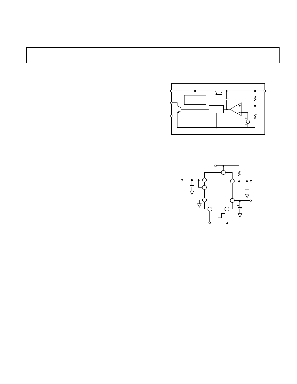
GENERAL DESCRIPTION
The ADP3302 is a member of the ADP330X family of precision
micropower low dropout anyCAP™ regulators. The ADP3302
contains two fully independent 100 mA regulators with separate
shutdown and merged error outputs. It features 1.4% overall
output accuracy and very low, 120 mV typical, dropout voltage.
The ADP3302 has a wide input voltage range from 13 V to
112 V. It features an error flag that signals when either of the
two regulators is about to lose regulation. It has short circuit
current protection as well as thermal shutdown.
The ADP3302’s enhanced lead frame design allows for a maximum power dissipation of 630 mW @ +70°C ambient temperature
and 1.0 W at room temperature without any external heat sink.
ERR
SD
ADP3302
FUNCTIONAL BLOCK DIAGRAM
(1/2 IS SHOWN)
IN
THERMAL
PROTECTION
Q2
Q1
DRIVER
GND
Figure 1. Application Circuit
ADP3302
CC
GM
BANDGAP
REF
OUT
R1
R2
anyCAP™ is a trademark of Analog Devices, Inc.
REV. 0
Information furnished by Analog Devices is believed to be accurate and
reliable. However, no responsibility is assumed by Analog Devices for its
use, nor for any infringements of patents or other rights of third parties
which may result from its use. No license is granted by implication or
otherwise under any patent or patent rights of Analog Devices.
One Technology Way, P.O. Box 9106, Norwood, MA 02062-9106, U.S.A.
Tel: 617/329-4700 World Wide Web Site: http://www.analog.com
Fax: 617/326-8703 © Analog Devices, Inc., 1997
Page 2
ADP3302–SPECIFICATIONS
(@ TA = –208C to +858C, VIN = 7 V, CIN = 0.47 mF, C
1
noted)
= 0.47 mF, unless otherwise
OUT
Parameter Symbol Conditions Min Typ Max Units
GROUND CURRENT I
GND
IL1 = IL2 = 100 mA 2 4 mA
IL1 = IL2 = 0.1 mA 0.4 0.8 mA
GROUND CURRENT IN DROPOUT I
GND
VIN = 2.5 V 1.0 2 mA
IL1 = IL2 = 0.1 mA
DROPOUT VOLTAGE V
DROP
V
OUT
I
= 100 mA 0.12 0.2 V
L
I
= 10 mA 0.05 0.1 V
L
IL = 1 mA 0.02 0.05 V
SHUTDOWN THRESHOLD V
THSD
ON 2.0 0.9 V
OFF 0.9 0.3 V
SHUTDOWN PIN INPUT CURRENT I
SDIN
0 < V
5 ≤ V
GROUND CURRENT IN SHUTDOWN I
Q
V
SDI
MODE @ V
V
SDI
@ V
OUTPUT CURRENT IN SHUTDOWN I
OSD
MODE T
ERROR PIN OUTPUT LEAKAGE I
ERROR PIN OUTPUT “LOW” VOLTAGE V
PEAK LOAD CURRENT I
THERMAL REGULATION V
OUTPUT NOISE V
NOTES
1
Ambient temperature of 185°C corresponds to a typical junction temperature of
Specifications subject to change without notice.
EL
EOL
LDPK
∆V
V
NOISE
O
O
T
= +85°C, @ VIN = 12 V 12 µA
A
= +25°C, @ VIN = 12 V 2 µA
A
V
= 5 V 13 µA
EO
I
SINK
VIN = Nominal V
= 12 V, IL = 100 mA 0.05 %/W
IN
T = 10 ms
f = 10 Hz–100 kHz, @ T
V
OUT
V
OUT
≤ 98% of V
< 5 V 0 1 µA
SD
≤ 12 V, @ VIN = 12 V 22 µA
SD
= V
SD2
=12 V 0 1 µA
IN
= V
SD2
=12 V 5 µA
IN
= 0, T
= 0, T
, Nominal
O
= +25°C,
A
= +85°C,
A
= 400 µA 0.15 0.3 V
+1 V 200 mA
OUT
= +25°C
A
= 3.3 V 75 µV rms
= 5 V 110 µV rms
+125°C.
ADP3302-3.0–SPECIFICATIONS
(@ TA = –208C to +858C, VIN = 3.3 V, CIN = 0.47 mF, C
otherwise noted)
= 0.47 mF, unless
OUT
Parameter Symbol Conditions Min Typ Max Units
OUTPUT VOLTAGE V
or VIN = 3.3 V to 12 V 2.976 3 3.024 V
OUT1
V
OUT2
IL = 0.1 mA to 100 mA
T
= +25°C
A
V
= 3.3 V to 12 V 2.958 3 3.042 V
IN
IL = 0.1 mA to 100 mA
∆V
or
∆V
∆V
∆I
∆V
∆I
IN
O
L
L2
∆V
O
01
∆I
= 3.3 V to 12 V 0.024 mV/V
IN
T
= +25°C, I
A
T
= +25°C
A
= 0.1 mA to 100 mA 1 µV/mA
L
T
= +25°C
A
02
L1
–2–
= 0.1 mA
L
REV. 0
LINE REGULATION V
LOAD REGULATION IL = 0.1 mA to 100 mA 0.030 mV/mA
CROSS REGULATION I
Specifications subject to change without notice.
Page 3
ADP3302
(@ TA = –208C to +858C, VIN = 3.5 V, CIN = 0.47 mF, C
ADP3302-3.2–SPECIFICATIONS
otherwise noted)
Parameter Symbol Conditions Min Typ Max Units
= 0.47 mF, unless
OUT
OUTPUT VOLTAGE V
or VIN = 3.5 V to 12 V 3.174 3.2 3.226 V
OUT1
V
OUT2
IL = 0.1 mA to 100 mA
T
= +25°C
A
V
= 3.5 V to 12 V 3.155 3.2 3.245 V
IN
IL = 0.1 mA to 100 mA
∆V
∆V
∆V
∆I
or
∆V
∆I
L2
O
L
01
O
IN
∆V
∆I
02
L1
LINE REGULATION V
LOAD REGULATION I
CROSS REGULATION I
Specifications subject to change without notice.
ADP3302-3.3–SPECIFICATIONS
= 3.5 V to 12 V 0.026 mV/V
IN
T
= +25°C, I
A
= 0.1 mA to 100 mA 0.032 mV/mA
L
T
= +25°C
A
= 0.1 mA to 100 mA 1 µV/mA
L
T
= +25°C
A
(@ TA = –208C to +858C, VIN = 3.6 V, CIN = 0.47 mF, C
= 0.1 mA
L
= 0.47 mF, unless
OUT
otherwise noted)
Parameter Symbol Conditions Min Typ Max Units
OUTPUT VOLTAGE V
or VIN = 3.6 V to 12 V 3.273 3.3 3.327 V
OUT1
V
OUT2
IL = 0.1 mA to 100 mA
T
= +25°C
A
V
= 3.6 V to 12 V 3.253 3.3 3.347 V
IN
IL = 0.1 mA to 100 mA
∆V
∆V
∆V
or
∆V
∆I
∆I
O
L
L2
O
IN
01
∆V
∆I
= 3.6 V to 12 V 0.026 mV/V
IN
T
= +25°C, I
A
= 0.1 mA to 100 mA 0.033 mV/mA
L
T
= +25°C
A
= 0.1 mA to 100 mA 1 µV/mA
L
T
= +25°C
A
02
L1
(@ TA = –208C to +858C, VIN = 5.3 V, CIN = 0.47 mF, C
= 0.1 mA
L
= 0.47 mF, unless
OUT
otherwise noted)
LINE REGULATION V
LOAD REGULATION I
CROSS REGULATION I
Specifications subject to change without notice.
ADP3302-5.0–SPECIFICATIONS
Parameter Symbol Conditions Min Typ Max Units
OUTPUT VOLTAGE V
or VIN = 5.3 V to 12 V 4.960 5.0 5.040 V
OUT1
V
OUT2
IL = 0.1 mA to 100 mA
T
= +25°C
A
V
= 5.3 V to 12 V 4.930 5.0 5.070 V
IN
IL = 0.1 mA to 100 mA
∆V
∆V
∆V
∆I
∆V
∆I
or
IN
L
L2
O
O
01
∆V
∆I
= 5.3 V to 12 V 0.04 mV/V
IN
T
= +25°C, I
A
= 0.1 mA to 100 mA 0.05 mV/mA
L
T
= +25°C
A
= 0.1 mA to 100 mA 1 µV/mA
L
T
= +25°C
A
02
L1
= 0.1 mA
L
–3–
LINE REGULATION V
LOAD REGULATION I
CROSS REGULATION I
Specifications subject to change without notice.
REV. 0
Page 4

ADP3302
WARNING!
ESD SENSITIVE DEVICE
IN
SD1
SD2
IN
OUT1
ERR
GND
OUT2
1
2
3
4
8
7
6
5
TOP VIEW
(Not to Scale)
ADP3302
ABSOLUTE MAXIMUM RATINGS*
Input Supply Voltage . . . . . . . . . . . . . . . . . . . .–0.3 V to +16 V
Please note: Pins 5 and 8 should be connected externally for proper operation.
Shutdown Input Voltage . . . . . . . . . . . . . . . . .–0.3 V to +16 V
Error Flag Output Voltage . . . . . . . . . . . . . . . . –0.3 V to +16 V
Power Dissipation . . . . . . . . . . . . . . . . . . . . Internally Limited
Operating Ambient Temperature Range . . . .–55°C to +125°C
Operating Junction Temperature Range . . . . –55°C to +125°C
θ
. . . . . . . . . . . . . . . . . . . . . . . . . . . . . . . . . . . . . . 96°C/W
JA
θ
. . . . . . . . . . . . . . . . . . . . . . . . . . . . . . . . . . . . . . 55°C/W
JC
Storage Temperature Range . . . . . . . . . . . . . –65°C to +150°C
Lead Temperature Range (Soldering 10 sec) . . . . . . . . +300°C
Vapor Phase (60 sec) . . . . . . . . . . . . . . . . . . . . . . . . +215°C
Infrared (15 sec) . . . . . . . . . . . . . . . . . . . . . . . . . . . +220°C
*This is a stress rating only; functional operation of the device at these or any other
conditions above those indicated in the operation section of this specification is not
implied. Exposure to absolute maximum rating conditions for extended periods
may affect device reliability.
ORDERING GUIDE
Voltage Package
Model
Outputs Option*
ADP3302AR1 OUT 1 3.0 V SO-8
OUT 2 3.0 V SO-8
ADP3302AR2 OUT 1 3.2 V SO-8
OUT 2 3.2 V SO-8
ADP3302AR3 OUT 1 3.3 V SO-8
OUT 2 3.3 V SO-8
ADP3302AR4 OUT 1 3.3 V SO-8
OUT 2 5.0 V SO-8
ADP3302AR5 OUT 1 5.0 V SO-8
OUT 2 5.0 V SO-8
NOTES
*SO = Small Outline Package.
Contact factory for availability of customized options available with mixed
output voltages.
PIN FUNCTION DESCRIPTIONS
Pin Name Function
1 OUT1 Output of Regulator 1, fixed 3.0 V, 3.2 V,
3.3 V or 5 V output voltage. Sources up to
200 mA. Bypass to ground with a 0.47 µF
capacitor.
2 ERR Open Collector Output. Active low indicates
that one of the two outputs is about to go out
of regulation.
3 GND Ground Pin.
4 OUT2 Output Regulator 2. Independent of Regula-
tor 1. Fixed 3.0 V, 3.2 V, 3.3 V or 5 V output
voltage. Bypass to ground with a 0.47 mF
capacitor.
5, 8 IN Regulator Input. Supply voltage can range
from 13.0 V to 112 V. Pins 5 and 8 must be
connected together for proper operation.
6 SD2 Active Low Shutdown Pin for Regulator 2.
Connect to ground to disable the Out 2 out-
put. When shutdown is not used, this pin
should be connected to the input pin.
7 SD1 Shutdown Pin for Regulator 1, otherwise
identical to SD2.
PIN CONFIGURATION
CAUTION
ESD (electrostatic discharge) sensitive device. Electrostatic charges as high as 4000 V readily
accumulate on the human body and test equipment and can discharge without detection.
Although the ADP3302 features proprietary ESD protection circuitry, permanent damage may
occur on devices subjected to high energy electrostatic discharges. Therefore, proper ESD
precautions are recommended to avoid performance degradation or loss of functionality.
–4–
REV. 0
Page 5

Typical Performance Characteristics–
TEMPERATURE – °C
GROUND CURRENT – µA
3000
0
–45 –25 135–5 15 35 75 95 11555
2500
2000
1500
1000
500
IL1 = 100mA
IL2 = 100mA
IL1 = 100mA
IL2 = 0mA
IL1 = 0mA
IL2 = 0mA
TIME – µs
0
0 100
200
2.0
VSD = V
IN
CL = 0.47µF
R
L
= 33Ω
1.0
3.0
4.0
5.0
6.0
7.0
8.0
20
INPUT/OUTPUT VOLTAGE – Volts
40 60 80 120 140 160 180
V
IN
V
OUT
ADP3302
5.001
5
IL = 1mA
4.999
IL = 20mA
4.998
4.997
OUTPUT VOLTAGE – Volts
4.996
4.995
5.1
IL = 0mA
IL = 100mA
6168101214
5.55.45.35.2
INPUT VOLTAGE – Volts
Figure 2. Line Regulation Output
Voltage vs. Supply Voltage on
ADP3302AR5
5
VIN = 7V
4
3
2
GROUND CURRENT – mA
1
0
050
IL1 = 0 TO 200mA
I
= 0 TO 200mA
L2
IL1 = 0 TO 200mA
I
= 0mA
L2
100 150 200
OUTPUT LOAD – mA
5.005
5.000
4.995
4.990
OUTPUT VOLTAGE – Volts
4.985
4.980
025
VIN = 7V
50 75
100 125 150 175 200
OUTPUT LOAD – mA
Figure 3. Output Voltage vs.
Load Current Up to 200 mA
on ADP3302AR5
0.2
0.1
0.0
–0.1
–0.2
OUTPUT VOLTAGE – %
–0.3
–0.4
–45 –25 135–5 15 35 75 95 11555
IL = 0
TEMPERATURE – °C
1.6
1.4
1.2
1.0
0.8
0.6
0.4
GROUND CURRENT – mA
0.2
0.0
3165 7 9 11 13
1
IL = IL2 =0
INPUT VOLTAGE – Volts
Figure 4. Quiescent Current vs.
Supply Voltage–ADP3302AR3
Figure 5. Quiescent Current vs. Load
Current
250
200
150
100
50
INPUT-OUTPUT VOLTAGE – mV
0
0 20 200
Figure 8. Dropout Voltage vs. Output
Current
REV. 0
40 60 80 100 120 140 160 180
OUTPUT LOAD – mA
Figure 6. Output Voltage Variation %
vs. Temperature
5
4
3
2
RL = 33Ω
1
INPUT/OUTPUT VOLTAGE – Volts
0
03 0
211
INPUT VOLTAGE – Volts
432
Figure 9. Power-Up/Power-Down on
ADP3302AR3.
SD
= 3 V or V
IN
–5–
Figure 7. Quiescent Current vs.
Temperature
Figure 10. Power-Up Transient on
ADP3302AR1
Page 6

ADP3302
–Typical Performance Characteristics
3.31
3.3
3.29
3.31
Volts
3.3
3.29
7.5
7
0 40 400
3.3kΩ, 0.47µF LOAD
33Ω, 0.47µF LOAD
V
IN
80 120 160 200 240 280 320 360
TIME – µs
Figure 11. Line Transient Response—
µ
F Load) on ADP3302AR4
(0.47
3.302
3.3
Volts
3.298
Volts
mA
CL = 10µF
5.03
5.01
5
4.99
4.97
100
0
0 1000
V
OUT1
V
OUT2
I (V
) 100mA
OUT2
200 400 600 800
TIME – µs
3.31
3.3
3.29
3.31
Volts
3.3
3.29
7.5
7
0 40 400
3.3kΩ, 10µF LOAD
33Ω, 10µF LOAD
V
IN
80 120 160 200 240 280 320 360
TIME – µs
Figure 12. Line Transient Response
(10
µ
F Load) on ADP3302AR4
3.305
3.3
Volts
3.295
5.002
5
Volts
4.998
100
mA
0
0 1000
Figure 13. Load Transient on
and Crosstalk of V
V
OUT1
ADP3302AR4 for 1 mA to 100 mA
Pulse
5
3.3V
0
0
12 34
05
TIME – sec
4
3
Volts
2
1
0
5
Volts
0
0 20 200
Volts
400
300
200
mA
100
3.5
V
OUT1
CL = 0.47µF
V
OUT2
I (V
) 100mA
OUT1
200 400 600 800
TIME – µs
OUT2
CL = 0.47µF
CL = 4.7µF
3V
40 60 80 100 120 140 160 180
TIME – µs
RL = 33Ω
3.3V
on
Figure 14. Load Transient on
and Crosstalk on V
V
OUT2
OUT1
on
ADP3302AR4 for 1 mA to 100 mA
Pulse
4
3
2
1
Volts
0
5
0
05 50
C = 0.47µF
R = 33Ω ON 3.3V OUTPUT
V
OUT
V
SD
10 15 20 25 30 35 40 45
TIME – µs
Figure 17. Turn Off on ADP3302AR3
Figure 15. Short Circuit Current
0
a. 0.47µF @ NO LOAD
–10
b. 0.47µF @ 33Ω
c. 10µF @ NO LOAD
–20
d. 10µF @ 33Ω
–30
–40
–50
–60
–70
b d
RIPPLE REJECTION – dB
–80
–90
a
c
–100
10 100 10M
1k 10k 100k 1M
FREQUENCY – Hz
b
d
c
Figure 18. Power Supply Ripple
Rejection on ADP3302AR3
Figure 16. Turn On ADP3302AR3
0.8
c
a
0.6
0.4
a. 0.47µF @ NO LOAD
a
0.2
b. 0.47µF @ 33Ω
c. 10µF @ NO LOAD
d. 10µF @ 33Ω
0
102 103 105
VOLTAGE NOISE SPECTRAL DENSITY – µV/ Hz
FREQUENCY = Hz
b d
0.47µF BYPASS
PIN 5, 8 TO PIN 3
a
c
104
b
d
Figure 19. Output Noise Density on
ADP3302AR5
–6–
REV. 0
Page 7

ADP3302
APPLICATION INFORMATION
anyCAP
™
The ADP3302 is an easy to use dual low dropout voltage
regulator. The ADP3302 requires only a very small 0.47 µF bypass
capacitor on the outputs for stability. Unlike the conventional
LDO designs, the ADP3302 is stable with virtually any type of
capacitors (anyCAP™) independent of the capacitor’s ESR
(Effective Series Resistance) value.
Capacitor Selection
Output Capacitors: As with any micropower device, output
transient response is a function of the output capacitance. The
ADP3302 is stable with a wide range of capacitor values, types
and ESR (anyCAP™). A capacitor as low as 0.47 mF is all that
is needed for stability. However, larger capacitors can be used if
high output current surges are anticipated. The ADP3302 is
stable with extremely low ESR capacitors (ESR ≈ 0), such as
multilayer ceramic capacitors (MLCC) or OSCON.
Input Bypass Capacitor: An input bypass capacitor is not
required. However, for applications where the input source is
high impedance or far from the input pins, a bypass capacitor is
recommended. Connecting a 0.47 mF capacitor from the input
pins (Pins 5 and 8) to ground reduces the circuit’s sensitivity to
PC board layout.
Low ESR capacitors offer better performance on a noisy supply;
however, for less demanding requirements a standard tantalum
or aluminum electrolytic capacitor is adequate.
Thermal Overload Protection
The ADP3302 is protected against damage due to excessive
power dissipation by its thermal overload protection circuit,
which limits the die temperature to a maximum of 165°C.
Under extreme conditions (i.e., high ambient temperature and
power dissipation) where die temperature starts to rise above
165°C, the output current is reduced until the die temperature
has dropped to a safe level. The output current is restored when
the die temperature is reduced.
Current and thermal limit protections are intended to protect
the device against accidental overload conditions. For normal
operation, device power dissipation should be externally limited
so that junction temperatures will not exceed 125°C.
Calculating Junction Temperature
Device power dissipation is calculated as follows:
PD = (V
Where I
I
GND
– V
IN
LOAD1
is ground current, VIN and V
OUT1
and I
) I
+ (V
– V
) I
LOAD1
LOAD2
IN
OUT2
are Load currents on Outputs 1 and 2,
are input and output
OUT
LOAD2
+ (VIN) I
GND
voltages respectively.
Assuming I
and V
OUT1
LOAD1
= V
= I
OUT2
LOAD2
= 100 mA, I
= 2 mA, VIN = 7.2 V
GND
= 5.0 V, device power dissipation is:
PD = (7.2 V – 5 V) 100 mA + (7.2 V – 5 V) 100 mA + (7.2 V)
2 mA = 0.454 W
The proprietary thermal coastline lead frame used in the
ADP3302 yields a thermal resistance of 96°C/W, which is significantly lower than a standard 8-pin SOIC package at 170°C/W.
Junction temperature above ambient temperature will be
approximately equal to:
0.454 W 3 96°C/W = 43.6°C
To limit the maximum junction temperature to 125°C, maximum ambient temperature must be lower than:
TA
= 125°C 2 43.6°C = 81.4°C
MAX
PRINTED CIRCUIT BOARD LAYOUT CONSIDERATION
All surface mount packages rely on the traces of the PC board to
conduct heat away from the package.
In standard packages the dominant component of the heat
resistance path is the plastic between the die attach pad and the
individual leads. In typical thermally enhanced packages one or
more of the leads are fused to the die attach pad, significantly
decreasing this component. However, to make the improvement
meaningful, a significant copper area on the PCB has to be
attached to these fused pins.
The ADP3302’s patented thermal coastline lead frame design
uniformly minimizes the value of the dominant portion of the
thermal resistance. It ensures that heat is conducted away by all
pins of the package. This yields a very low 96°C/W thermal
resistance for an SO-8 package, without any special board layout requirements, relying just on the normal traces connected to
the leads. The thermal resistance can be decreased by, approximately, an additional 10% by attaching a few square cm of
copper area to the two V
pins of the ADP3302 package.
IN
It is not recommended to use solder mask or silkscreen on the
PCB traces adjacent to the ADP3302 pins since it will increase
the junction to ambient thermal resistance of the package.
Shutdown Mode
Applying a TTL high signal to the shutdown pin or tying it to
the input pin will turn the output ON. Pulling the shutdown pin
down to a TTL low signal or tying it to ground will turn the
output OFF. Outputs are independently controlled. In shutdown
mode, quiescent current is reduced to less than 2 mA.
Error Flag Dropout Detector
The ADP3302 will maintain its output voltage over a wide
range of load, input voltage and temperature conditions. If
regulation is lost, for example, by reducing the supply voltage
below the combined regulated output and dropout voltages, the
ERRor flag will be activated. The ERR output is an open
collector, which will be driven low.
Once set, the ERRor flag’s hysteresis will keep the output low
until a small margin of operating range is restored, either by
raising the supply voltage or reducing the load.
A single ERR pin serves both regulators in the ADP3302 and
indicates that one or both regulators are on the verge of losing
regulation.
APPLICATION CIRCUIT
Dual Post Regulator Circuit for Switching Regulators
The ADP3302 can be used to implement a dual 3 V/100 mA
post regulator power supply from a 1 cell Li-Ion input (Figure
20). This circuit takes 2.5 V to 4.2 V as the input and delivers
dual 3 V/100 mA outputs. Figure 21 shows the typical efficiency
curve.
For ease of explanation, let’s partition the circuit into the
ADP3000 step-up regulator section and the ADP3302 low
dropout regulation section. Furthermore, let’s divide the operation
of this application circuit into the following three phases.
REV. 0
–7–
Page 8

ADP3302
2
OUT1
IN
1
8
ERR
V
OUT1
3.3V
C5
1µF
5
V
IN
= 6V TO 12V
GND
SD1
IN
OUT2
V
OUT2
5.0V
SD2
C2
0.01µF
C1
0.01µF
C4
0.5µF
C3
0.5µF
ON/OFF
3.3V
D2
D1
R2
220kΩ
R1
220kΩ
D3
R3
330kΩ
4
7
6
3
ADP3302
2.5V → 4.2V
1MΩ
R4
120kΩ
V
I
IN
LIM
SET
R3
ADP3000
A
O
GND SW2
SW1
R1
100kΩ
100µF
C1
10V
AVX-TPS
R2
90kΩ
FB
R5
330kΩ
Q1
2N2907
R6
100kΩR810kΩ
C2
33nF
R7
90kΩ
Figure 20. Cell Li-Ion to 3 V/200 mA Converter with Shutdown at VIN < 2.5 V
Phase One: When the input voltage is equal to 3.7 V or higher,
the ADP3000 is off and the ADP3302 operates on its own to
regulate the output voltage. At this phase, current is flowing into
the input pins of the ADP3302 via the inductor L1 and the
Schottky diode. At the same time, the ADP3000 is set into sleep
mode by pulling the FB pin (via R9 and R10 resistor divider
network) to about 10% higher than its internal reference which
is set to be 1.245 V.
Phase Two: As the input voltage drops below 3.7 V, the
decreasing input voltage causes the voltage of the FB pin to be
within 5% of the 1.245 V reference. This triggers the ADP3000
to turn on, providing a 3.4 V regulated output to the inputs of
the ADP3302. The ADP3000 continues to supply the 3.4 V
regulated voltage to the ADP3302 until the input voltage drops
below 2.5 V.
Phase Three: When the input voltage drops below 2.5 V, the
ADP3302 will shut down and the ADP3000 will go into sleep
mode. With the input voltage below 2.5 V, the resistor divider
network, R1 and R2, applies a voltage that is lower than the
ADP3000’s internal 1.245 V reference voltage to the SET pin.
This causes the A
pin to have a voltage close to 0 V, which
O
causes the ADP3302 to go into shutdown directly and Q1 to
turn on and pull the FB pin 10% or higher than the internal
1.245 V reference voltage. With the FB pin pulled high, the
ADP3000 goes into sleep mode.
AT V
≤ 2.5V
80
75
70
% EFFICIENCY
65
2.6 3.0 3.4 3.8 4.2
IO = 50mA + 50mA
= 100mA + 100mA
I
O
IN
SHDN IQ = 500µA
V
IN
(V)
(SUMIDA–CDRH62)
L1
6.6µF
IN5817
R9
348kΩ
1%
R10
200kΩ
1%
C3
100µF
10V
AVX-TPS
IN
IN
ADP3302
SD
GND
V
O2
V
O2
1µF
6V
(MLC)
1µF
6V
(MLC)
3V
100mA
C4
C5
3V
100mA
Supply Sequencing Circuit
Figure 22 shows a simple and effective way to achieve sequencing of two different output voltages, 3.3 V and 5 V, in a mixed
supply voltage system. In most cases, these systems need careful
sequencing for the supplies to avoid latchup.
At turn-on, D1 rapidly charges up C1 and enables the 5 V output. After a R2-C2 time constant delay, the 3.3 V output is
enabled. At turn-off, D2 quickly discharges C2 and R3 pulls
SD1 low, turning off the 3.3 V output first. After a R1-C1 time
constant delay, the 5 V output turns off.
Figure 22. Turn-On/Turn-Off Sequencing for Mixed Supply
Voltages
OUTLINE DIMENSIONS
Dimensions shown in inches and (mm).
8-Pin SOIC
(SO-8)
0.1968 (5.00)
0.1890 (4.80)
8
0.1574 (4.00)
0.1497 (3.80)
5
0.2440 (6.20)
41
0.2284 (5.80)
C2989-12-1/97
Figure 21. Typical Efficiency of the Circuit of Figure 20
Refer to Figure 20. R9 and R10 set the output voltage of the
ADP3000. R1, R2, and R3 set the shutdown threshold voltage
for the circuit. For further details on the ADP3000, please refer
to the ADP3000 data sheet.
–8–
PIN 1
0.0098 (0.25)
0.0040 (0.10)
SEATING
PLANE
0.0500
(1.27)
BSC
0.0688 (1.75)
0.0532 (1.35)
0.0192 (0.49)
0.0138 (0.35)
0.0098 (0.25)
0.0075 (0.19)
0.0196 (0.50)
0.0099 (0.25)
8°
0°
0.0500 (1.27)
0.0160 (0.41)
x 45°
PRINTED IN U.S.A.
REV. 0
 Loading...