

Datasheet ADP3300ART-5, ADP3300ART-3.3, ADP3300ART-3.2, ADP3300ART-3, ADP3300ART-2.7 Datasheet (Analog Devices)
Page 1
High Accuracy anyCAP
E
®
a
50 mA Low Dropout Linear Regulator
FEATURES
High Accuracy Over Line and Load: ⴞ0.8% @ 25ⴗC,
ⴞ1.4% Over Temperature
Ultralow Dropout Voltage: 80 mV Typical @ 50 mA
Requires Only C
= 0.47 F for Stability
O
anyCAP = Stable with All Types of Capacitors
(Including MLCC)
Current and Thermal Limiting
Low Noise
Dropout Detector
Low Shutdown Current: 1 A
3.0 V to 12 V Supply Range
–40ⴗC to +85ⴗC Ambient Temperature Range
Several Fixed Voltage Options
Ultrasmall SOT-23 6-Lead Package
Excellent Line and Load Regulation
APPLICATIONS
Cellular Telephones
Notebook, Palmtop Computers
Battery Powered Systems
PCMCIA Regulators
Bar Code Scanners
Camcorders, Cameras
GENERAL DESCRIPTION
The ADP3300 is a member of the ADP330x family of precision
low dropout anyCAP voltage regulators. The ADP3300 stands
out from conventional LDOs with a novel architecture and an
enhanced process. Its patented design requires only a 0.47 µF
output capacitor for stability. This device is stable with any
capacitor, regardless of its ESR (Equivalent Series Resistance)
value, including ceramic types (MLCC) for space restricted applications. The ADP3300 achieves exceptional accuracy of ±0.8%
at room temperature and ± 1.4% overall accuracy over temperature, line and load variations. The dropout voltage of the
ADP3300 is only 80 mV (typical) at 50 mA.
The ADP3300 operates with a wide input voltage range from
3.0 V to 12 V and delivers a load current in excess of 50 mA.
It features an error flag that signals when the device is about to
lose regulation or when the short circuit or thermal overload
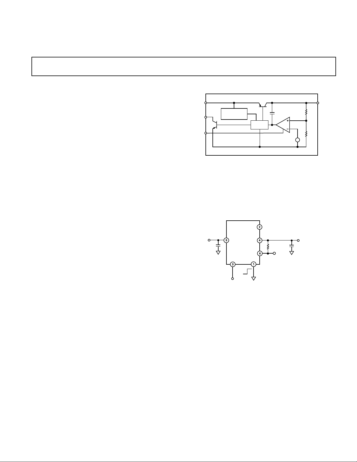
ADP3300
FUNCTIONAL BLOCK DIAGRAM
CC
BANDGAP
R1
330k⍀
E
ADP3300
g
m
REF
+
OUT
+
–
C2
0.47F
OUT
R1
R2
V
= +5V
OUT
IN
RR
SD
V
IN
0.47F
Q2
C1
THERMAL
PROTECTION
+
ADP3300-5
IN
ON
OFF
SD
Q1
DRIVER
GND
NR
OUT
ERR
GND
Figure 1. Typical Application Circuit
protection is activated. Other features include shutdown and
optional noise reduction capabilities. The ADP330x anyCAP LDO
family offers a wide range of output voltages and output current
levels from 50 mA to 200 mA:
ADP3301 (100 mA)
ADP3302 (100 mA, Dual Output)
ADP3303 (200 mA)
anyCAP is a registered trademark of Analog Devices Inc.
REV. B
Information furnished by Analog Devices is believed to be accurate and
reliable. However, no responsibility is assumed by Analog Devices for its
use, nor for any infringements of patents or other rights of third parties that
may result from its use. No license is granted by implication or otherwise
under any patent or patent rights of Analog Devices.
One Technology Way, P.O. Box 9106, Norwood, MA 02062-9106, U.S.A.
Tel: 781/329-4700 www.analog.com
Fax: 781/326-8703 © Analog Devices, Inc., 2001
Page 2
ADP3300–SPECIFICATIONS
(@ TA = –40ⴗC to +85ⴗC, VIN = 7 V, CIN = 0.47 F, C
otherwise noted)
= 0.47 F, unless
OUT
Parameter Symbol Conditions Min Typ Max Unit
OUTPUT VOLTAGE V
OUT
ACCURACY I
VIN = V
T
V
OUT(NOM)
= 0.1 mA to 50 mA
L
= 25°C –0.8 +0.8 %
A
= V
IN
OUT(NOM)
0.3 V to 12 V
0.3 V to 12 V
IL = 0.1 mA to 50 mA –1.4 +1.4 %
LINE REGULATION ∆V
∆V
LOAD REGULATION ∆V
∆I
GROUND CURRENT I
GND
O
IN
O
L
= V
IN
OUT(NOM)
TA = 25°C 0.02 mV/V
IL = 0.1 mA to 50 mA
TA = 25°C 0.06 mV/mA
IL = 50 mA 0.55 1.7 mA
0.3 V to 12 V
V
IL = 0.1 mA 0.19 0.3 mA
GROUND CURRENT I
GND
VIN = 2.5 V
IN DROPOUT IL = 0.1 mA 0.6 1.2 mA
DROPOUT VOLTAGE V
DROP
V
= 98% of V
OUT
OUT(NOM)
IL = 50 mA 0.08 0.17 V
I
= 10 mA 0.025 0.07 V
L
IL = 1 mA 0.004 0.03 V
SHUTDOWN THRESHOLD V
THSD
ON 2.0 0.75 V
OFF 0.75 0.3 V
SHUTDOWN PIN I
SDIN
0 < V
INPUT CURRENT 5 < V
GROUND CURRENT IN I
Q
VSD = 0, VIN = 12 V
SHUTDOWN MODE T
V
≤ 5 V 1 µA
SD
≤ 12 V @ VIN = 12 V 22 µA
SD
= 25°C 0.005 1 µA
A
= 0, VIN = 12 V
SD
TA = 85°C0.013µA
OUTPUT CURRENT IN I
OSD
TA = 25°C @ VIN = 12 V 2 µA
SHUTDOWN MODE TA = 85°C @ VIN = 12 V 4 µA
ERROR PIN OUTPUT
LEAKAGE I
EL
VEO = 5 V 13 µA
ERROR PIN OUTPUT
“LOW” VOLTAGE V
PEAK LOAD CURRENT I
OUTPUT NOISE V
EOL
LDPK
NOISE
@ 5 V OUTPUT C
I
= 400 µA 0.12 0.3 V
SINK
VIN = V
OUT(NOM)
1 V 100 mA
f = 10 Hz–100 kHz
= 0 100 µV rms
NR
CNR = 10 nF, CL = 10 µF30µV rms
NOTE
Ambient temperature of +85°C corresponds to a typical junction temperature of 125 °C under typical full load test conditions.
Specifications subject to change without notice.
–2–
REV. B
Page 3
ADP3300
WARNING!
ESD SENSITIVE DEVICE
ABSOLUTE MAXIMUM RATINGS*
Input Supply Voltage . . . . . . . . . . . . . . . . . . . . –0.3 V to +16 V
Shutdown Input Voltage . . . . . . . . . . . . . . . . . –0.3 V to +16 V
Error Flag Output Voltage . . . . . . . . . . . . . . . . –0.3 V to +16 V
Noise Bypass Pin Voltage . . . . . . . . . . . . . . . . . –0.3 V to +5 V
Power Dissipation . . . . . . . . . . . . . . . . . . . . Internally Limited
Operating Ambient Temperature Range . . . . –55°C to +125°C
Operating Junction Temperature Range . . . . –55°C to +125°C
. . . . . . . . . . . . . . . . . . . . . . . . . . . . . . . . . . . . . . 165°C/W
θ
JA
θ
. . . . . . . . . . . . . . . . . . . . . . . . . . . . . . . . . . . . . . . 92°C/W
JC
Storage Temperature Range . . . . . . . . . . . . . –65°C to +150°C
Lead Temperature Range (Soldering 10 sec) . . . . . . . . . . 300°C
Vapor Phase (60 sec ) . . . . . . . . . . . . . . . . . . . . . . . . . . 215°C
Infrared (15 sec) . . . . . . . . . . . . . . . . . . . . . . . . . . . . . 220°C
*This is a stress rating only; operation beyond these limits can cause the device to
be permanently damaged.
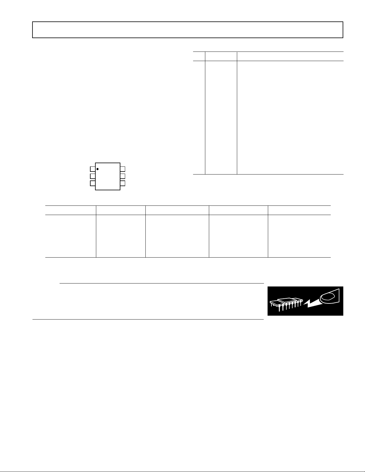
PIN CONFIGURATION
Pin Mnemonic Function
1 GND Ground Pin
2 NR Noise Reduction Pin. Used for further
3 SD Active Low Shutdown Pin. Connect to
4 OUT Output of the Regulator, fixed 2.7, 3.0, 3.2,
5 IN Regulator Input
6 ERR Open Collector Output which goes low to
PIN FUNCTION DESCRIPTIONS
reduction of the output noise (see text for
details). No connection if not used.
ground to disable the regulator output.
When shutdown is not used, this pin should
be connected to the input pin.
3.3 or 5 volts output voltage. Bypass to
ground with a 0.47 µF or larger capacitor.
indicate that the output is about to go out
GND
NR
SD
1
ADP3300
2
TOP VIEW
(Not to Scale)
3
6
ERR
5
IN
OUT
4
of regulation.
ORDERING GUIDE
Model Voltage Output Package Description Package Options Branding Information
ADP3300ART-2.7 2.7 V Surface Mount SOT-23-6 LAB
ADP3300ART-2.85 2.85 V Surface Mount SOT-23-6 LFB
ADP3300ART-3 3.0 V Surface Mount SOT-23-6 LBB
ADP3300ART-3.2 3.2 V Surface Mount SOT-23-6 LCB
ADP3300ART-3.3 3.3 V Surface Mount SOT-23-6 LDB
ADP3300ART-5 5.0 V Surface Mount SOT-23-6 LEB
Contact the factory for the availability of other output voltage options.
CAUTION
ESD (electrostatic discharge) sensitive device. Electrostatic charges as high as 4000 V readily
accumulate on the human body and test equipment and can discharge without detection. Although
the ADP3300 features proprietary ESD protection circuitry, permanent damage may occur on
devices subjected to high-energy electrostatic discharges. Therefore, proper ESD precautions are
recommended to avoid performance degradation or loss of functionality.
REV. B
–3–
Page 4

ADP3300–Typical Performance Characteristics
3.202
3.201
3.200
3.199
3.198
OUTPUT VOLTAGE – Volts
3.197
3.196
3.3 144 5 6 7 8 9 10 11 12 13
IL = 0mA
IL = 10mA
V
OUT
IL = 50mA
INPUT VOLTAGE – Volts
= 3.2V
TPC 1. Line Regulation Output
Voltage vs. Supply Voltage
820
690
560
430
300
GROUND CURRENT – A
IL = 0 TO 80mA
= 7V
V
IN
3.202
V
3.201
3.200
3.199
3.198
3.197
OUTPUT VOLTAGE – Volts
3.196
3.195
0808 1624324048 566472
OUTPUT LOAD – mA
= 3.2V
OUT
= 7V
V
IN
TPC 2. Output Voltage vs. Load
Current
0.2
0.1
0.0
IL = 0 – 50mA
–0.1
–0.2
OUTPUT VOLTAGE – %
–0.3
800
V
640
480
320
160
GROUND CURRENT – A
0
0 12.01.2 2.4 3.6 4.8 6.0 7.2 8.4 9.6 10.8
INPUT VOLTAGE – Volts
OUT
= 0mA
I
L
TPC 3. Quiescent Current vs.
Supply Voltage
700
600
= 50mA
I
500
400
300
200
GROUND CURRENT – A
100
L
IL = 0mA
= 3.2V
VIN = 7V
170
08020 40 60
OUTPUT LOAD – mA
TPC 4. Quiescent Current vs.
Load Current
120
96
72
48
24
INPUT/OUTPUT VOLTAGE – mV
0
08020 40 60
OUTPUT LOAD – mA
TPC 7. Dropout Voltage
vs. Output Current
–0.4
–51535 759511555
–45 –25 135
TEMPERATURE – ⴗC
TPC 5. Output Voltage Variation % vs. Temperature
5
4
3
2
1
INPUT/OUTPUT VOLTAGE – Volts
0
03 0
RL = 33⍀
211
INPUT VOLTAGE – Volts
V
OUT
= 64⍀
R
L
432
= 3.2V
TPC 8. Power-Up/Power-Down
0
–25 –51535557595115135
–45
TEMPERATURE – ⴗC
TPC 6. Quiescent Current vs.
Temperature
8.0
7.0
6.0
5.0
4.0
3.0
2.0
1.0
INPUT/OUTPUT VOLTAGE – Volts
0
40 60 80 120 140 160 180
0 100
20
V
V
TIME – s
IN
OUT
VSD = V
CL = 0.47F
R
L
V
OUT
= 66⍀
TPC 9. Power-Up Overshoot
IN
= 3.3V
200
–4–
REV. B
Page 5

ADP3300
3.220
V
= 3.2V
OUT
3.210
3.200
3.190
3.180
RL = 3.2k⍀
= 0.47F
C
L
VOLTS
7.5
V
IN
7.0
0 20020 40 60 80 100 120 140 160 180
TIME – s
TPC 10. Line Transient Response
3.220
V
= 3.2V
OUT
= 4.7F
C
L
3.205
3.200
VOLTS
3.195
3.190
I
= 50mA
50
mA
1
OUT
1mA
3.220
V
= 3.2V
3.210
OUT
3.200
3.190
3.180
RL = 64⍀
= 0.47F
C
L
VOLTS
7.5
7.0
0
20 40 60 80 100 120 140 160
TIME – s
180
TPC 11. Line Transient Response
V
= 3.0V
3.0
VOLTS
200
150
100
mA
50
OUT
0
0
V
OUT
I
OUT
V
= 7V
IN
200
3.220
V
= 3.2V
OUT
3.205
= 0.47F
C
L
3.200
VOLTS
3.195
3.190
I
= 50mA
50
mA
1
0 1000200 400 600 800
OUT
TIME – s
TPC 12. Load Transient
4
CL = 0.47F
3
2
1
VOLTS
0
+3
0
CL = 4.7F
V
OUT
R
L
3V
1mA
3.2V
= 64⍀
V
OUT
= 3.2V
V
SD
0 1000200 400 600 800
TIME – s
TPC 13. Load Transient
4
3.2V
3
2
1
VOLTS
0
3
0
VOLTS
0 10020 40 60 80
TIME – s
TPC 16. Turn Off
V
R
C
V
SD
= 3.2V
OUT
= 64⍀
L
= 0.47F
L
0512 34
TIME – sec
TPC 14. Short Circuit Current
0
a. 0.47F, RL = 33k⍀
–10
b. 0.47F, RL = 64⍀
–20
c. 4.7F, RL = 33k⍀
d. 4.7F, R
–30
= 64⍀
L
–40
–50
–60
b
–70
d
RIPPLE REJECTION – dB
–80
–90
a c
–100
10 100 10M1k 10k 100k
FREQUENCY – Hz
V
a
TPC 17. Power Supply Ripple
Rejection
OUT
c
= 3.3V
b
d
1M
0 10020 40 60 80
TIME – s
TPC 15. Turn On
10
V
= 5V, C
= 0.47F,
OUT
= 1mA, C
I
L
L
=
NR
V
I
1
0.1
V
= 2.7-5.0V, CL = 0.47F,
OUT
1mA, C
=
I
L
0.01
100 1k 100k
VOLTAGE NOISE SPECTRAL DENSITY – V/ Hz
= 10nF
NR
V
OUT
= 1mA, C
I
L
FREQUENCY – Hz
0.47F BYPASS
PIN 5 TO PIN 1
0
= 3.3V, CL = 0.47F,
OUT
= 1mA, CNR = 0
L
= 2.7-5.0V, CL = 0.47F,
= 10nF
NR
10k
TPC 18. Output Noise Density
REV. B
–5–
Page 6

ADP3300
THEORY OF OPERATION
The new anyCAP LDO ADP3300 uses a single control loop for
regulation and reference functions. The output voltage is sensed
by a resistive voltage divider consisting of R1 and R2 which is
varied to provide the available output voltage option. Feedback
is taken from this network by way of a series diode (D1) and
a second resistor divider (R3 and R4) to the input of an amplifier.
D1
R3
PTAT
CURRENT
OUTPUT
R1
)
R2
(a)
R
LOAD
C
LOAD
INPUT
Q1
NONINVERTING
WIDEBAND
DRIVER
ADP3300
COMPENSATION
CAPACITOR
PTAT
V
OS
g
m
ATTENUATION
(V
BANDGAP/VOUT
R4
Figure 2. Functional Block Diagram
A very high gain error amplifier is used to control this loop. The
amplifier is constructed in such a way that at equilibrium it
produces a large, temperature proportional input “offset voltage”
that is repeatable and very well controlled. The temperatureproportional offset voltage is combined with the complimentary
diode voltage to form a “virtual bandgap” voltage, implicit in
the network, although it never appears explicitly in the circuit.
Ultimately, this patented design makes it possible to control the
loop with only one amplifier. This technique also improves the
noise characteristics of the amplifier by providing more flexibility
on the trade-off of noise sources that leads to a low noise design.
The R1, R2 divider is chosen in the same ratio as the bandgap
voltage to the output voltage. Although the R1, R2 resistor
divider is loaded by the diode D1 and a second divider consisting
of R3 and R4, the values are chosen to produce a temperature
stable output. This unique arrangement specifically corrects for
the loading of the divider so that the error resulting from base
current loading in conventional circuits is avoided.
The patented amplifier controls a new and unique noninverting
driver that drives the pass transistor, Q1. The use of this special
noninverting driver enables the frequency compensation to
include the load capacitor in a pole splitting arrangement to
achieve reduced sensitivity to the value, type and ESR of the
load capacitance.
Most LDOs place strict requirements on the range of ESR
values for the output capacitor because they are difficult to
stabilize due to the uncertainty of load capacitance and resistance. Moreover, the ESR value, required to keep conventional
LDOs stable, changes depending on load and temperature.
These ESR limitations make designing with LDOs more difficult because of their unclear specifications and extreme variations
over temperature.
This is no longer true with the ADP3300 anyCAP LDO. It can
be used with virtually any capacitor, with no constraint on the
minimum ESR. The innovative design allows the circuit to be
stable with just a small 0.47 µF capacitor on the output. Addi-
tional advantages of the pole splitting scheme include superior line
noise rejection and very high regulator gain, which leads to excellent line and load regulation. An impressive ±1.4% accuracy is
guaranteed over line, load and temperature.
Additional features of the circuit include current limit, thermal
shutdown and noise reduction. Compared to the standard solutions that give warning after the output has lost regulation,
the ADP3300 provides improved system performance by enabling
the ERR pin to give warning before the device loses regulation.
As the chip’s temperature rises above 165°C, the circuit activates a
soft thermal shutdown, indicated by a signal low on the ERR
pin, to reduce the current to a safe level.
To reduce the noise gain of the loop, the node of the main
divider network (a) is made available at the noise reduction (NR)
pin, which can be bypassed with a small capacitor (10 nF–100 nF).
APPLICATION INFORMATION
Capacitor Selection: anyCAP
Output Capacitors: as with any micropower device, output
transient response is a function of the output capacitance. The
ADP3300 is stable with a wide range of capacitor values, types
and ESR (anyCAP). A capacitor as low as 0.47 µF is all that is
needed for stability. However, larger capacitors can be used if
high output current surges are anticipated. The ADP3300 is
stable with extremely low ESR capacitors (ESR ≈ 0), such as
multilayer ceramic capacitors (MLCC) or OSCON.
Input Bypass Capacitor: an input bypass capacitor is not
required; however, for applications where the input source is high
impedance or far from the input pins, a bypass capacitor is recommended. Connecting a 0.47 µF capacitor from the input to
ground reduces the circuit’s sensitivity to PC board layout. If a
bigger output capacitor is used, the input capacitor should be 1 µF
minimum.
Noise Reduction
A noise reduction capacitor (CNR) can be used to further reduce
the noise by 6 dB–10 dB (Figure 3). Low leakage capacitors in
the 10 nF–100 nF range provide the best performance. For load
current less than 200 µA, a 4.7 µF output capacitor provides the
lowest noise and the best overall performance. Since the noise
reduction pin (NR) is internally connected to a high impedance
node, any connection to this node should be carefully done to
avoid noise pickup from external sources. The pad connected to
this pin should be as small as possible. Long PC board traces
are not recommended.
V
IN
1.0F
NR
ADP3300-5
IN
+
C1
SD
OUT
ERR
ON
OFF
GND
C
NR
10nF
330k⍀
V
= 5V
OUT
+
C2
4.7F
E
OUT
Figure 3. Noise Reduction Circuit
–6–
REV. B
Page 7

ADP3300
VIN = 6V TO 8V
V
OUT
= 5V @ 1A
MJE253*
C2
10F
C1
47F
R1
50⍀
*AAVID531002 HEAT SINK IS USED
IN
OUT
ERR
GND
SD
ADP3300-5
+
Thermal Overload Protection
The ADP3300 is protected against damage due to excessive
power dissipation by its thermal overload protection circuit,
which limits the die temperature to a maximum of 165°C.
Under extreme conditions (i.e., high ambient temperature
and high power dissipation), where die temperature starts to rise
above 165°C, the output current is reduced until die temperature has dropped to a safe level. Output current is restored
when the die temperature is reduced.
Current and thermal limit protections are intended to protect
the device against accidental overload conditions. For normal
operation, device power dissipation should be externally
limited so that junction temperatures will not exceed 125°C.
Calculating Junction Temperature
Device power dissipation is calculated as follows:
PD = (V
Where I
V
and V
IN
Assuming I
V
= 3.3 V, device power dissipation is:
OUT
and I
LOAD
are input and output voltages respectively.
OUT
LOAD
– V
) I
IN
OUT
are load current and ground current,
GND
= 50 mA, I
GND
+ (VIN) I
LOAD
GND
= 0.5 mA, VIN = 8 V and
PD = (8 – 3.3) 0.05 + 8 × 0.5 mA = 0.239 W
∆T = TJ – TA = PD × θJA = 0.239 × 165 = 39.4°C
With a maximum junction temperature of 125°C, this yields a
maximum ambient temperature of 85°C.
Printed Circuit Board Layout Consideration
Surface mount components rely on the conductive traces or
pads to transfer heat away from the device. Appropriate PC
board layout techniques should be used to remove heat from the
immediate vicinity of the package.
The following general guidelines will be helpful when designing
a board layout:
1. PC board traces with larger cross section areas will remove
more heat. For optimum results, use PC boards with thicker
copper and wider traces.
2. Increase the surface area exposed to open air so heat can be
removed by convection or forced air flow.
3. Do not use solder mask or silkscreen on the heat dissipating
traces because it will increase the junction to ambient thermal
resistance of the package.
Shutdown Mode
Applying a high signal to the shutdown pin or tying it to the
input pin will turn the output ON. Pulling the shutdown pin
down to 0.3 V or below, or tying it to ground, will turn the
output OFF. In shutdown mode, quiescent current is reduced
to less than 1 µA.
Error Flag Dropout Detector
The ADP3300 will maintain its output voltage over a wide
range of load, input voltage and temperature conditions. If the
output is about to lose regulation, for example, by reducing the
supply voltage below the combined regulated output and dropout
voltages, the ERR pin will be activated. The ERR output is an
open collector that will be driven low.
Once set, the ERRor flag’s hysteresis will keep the output low
until a small margin of operating range is restored either by
raising the supply voltage or reducing the load.
APPLICATION CIRCUITS
Crossover Switch
The circuit in Figure 4 shows that two ADP3300s can be used
to form a mixed supply voltage system. The output switches
between two different levels selected by an external digital input.
Output voltages can be any combination of voltages from the
Ordering Guide.
V
C2
0.47F
OUT
= 5V/3.3V
= 5.5V TO 12V
V
IN
OUTPUT SELECT
5.0V
0V
1.0F
IN
ADP3300-5.0
SD
IN
+
C1
ADP3300-3.3
SD
GND
GND
OUT
OUT
+
Figure 4. Crossover Switch
Higher Output Current
If higher current is needed, an appropriate pass transistor can be
used, as in Figure 5, to increase the output current to 1 A.
Figure 5. High Output Current Linear Regulator
REV. B
–7–
Page 8

ADP3300
Constant Dropout Post Regulator
The circuit in Figure 6 provides high precision with low dropout for any regulated output voltage. It significantly reduces the
ripple from a switching regulator while providing a constant
dropout voltage, which limits the power dissipation of the LDO
to 15 mW. The ADP3000 used in this circuit is a switching
regulator in the step-up configuration.
D1
1N5817
FB
VIN = 2.5V TO 3.5V
100F
10V
L1
6.8H
C1
R1
120⍀
I
V
LIM
IN
SW1
ADP3000-ADJ
GND
SW2
Figure 6. Constant Dropout Post Regulator
OUTLINE DIMENSIONS
Dimensions shown in inches and (mm).
C2
100F
10V
2N3906
Q1
R2
30.1k⍀
1%
R3
124k⍀
1%
ADP3300-5
IN
SD
GND
OUT
Q2
2N3906
R4
274k⍀
5V @ 50mA
C3
2.2F
C00132–0–7/01(B)
6-Lead Surface Mount Package
(SOT-23)
0.122 (3.10)
0.106 (2.70)
2
0.075
(1.90)
BSC
0.020 (0.50)
0.010 (0.25)
4 5
0.037
(0.95) BSC
0.118 (3.00)
0.098 (2.50)
0.057 (1.45)
0.035 (0.90)
SEATING
PLANE
0.009 (0.23)
0.003 (0.08)
10ⴗ
0ⴗ
0.022 (0.55)
0.014 (0.35)
0.071 (1.80)
0.059 (1.50)
0.051 (1.30)
0.035 (0.90)
0.006 (0.15)
0.000 (0.00)
6
1 3
PIN 1
ADP3300–Revision History
Location Page
Data Sheet changed from REV. A to REV. B.
Edits to FEATURES . . . . . . . . . . . . . . . . . . . . . . . . . . . . . . . . . . . . . . . . . . . . . . . . . . . . . . . . . . . . . . . . . . . . . . . . . . . . . . . . . . . . . 1
Edits to GENERAL DESCRIPTION . . . . . . . . . . . . . . . . . . . . . . . . . . . . . . . . . . . . . . . . . . . . . . . . . . . . . . . . . . . . . . . . . . . . . . . . 1
Edits to ABSOLUTE MAXIMUM RATINGS . . . . . . . . . . . . . . . . . . . . . . . . . . . . . . . . . . . . . . . . . . . . . . . . . . . . . . . . . . . . . . . . . 3
Addition to the ORDERING GUIDE . . . . . . . . . . . . . . . . . . . . . . . . . . . . . . . . . . . . . . . . . . . . . . . . . . . . . . . . . . . . . . . . . . . . . . . . 3
PRINTED IN U.S.A.
–8–
REV. B
 Loading...