

Page 1
查询ADP3158供应商查询ADP3158供应商
4-Bit Programmable
a
FEATURES
Optimally Compensated Active Voltage Positioning
with Gain and Offset Adjustment (ADOPT™) for
Superior Load Transient Response
Complies with VRM Specifications with Lowest
System Cost
4-Bit Digitally Programmable 1.3 V to 2.05 V Output
N-Channel Synchronous Buck Driver
Total Accuracy 0.8% Over Temperature
Two On-Board Linear Regulator Controllers Designed
to Meet System Power Sequencing Requirements
High Efficiency Current-Mode Operation
Short Circuit Protection for Switching Regulator
Overvoltage Protection Crowbar Protects Micro-
processors with No Additional External Components
APPLICATIONS
Core Supply Voltage Generation for:
Intel Pentium
Intel Celeron™
®
III
Synchronous Buck Controllers
ADP3158/ADP3178
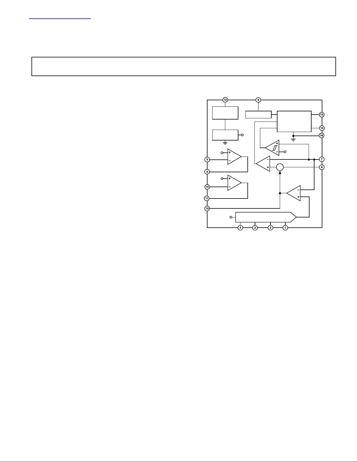
FUNCTIONAL BLOCK DIAGRAM
VCC CT
ADP3158/ADP3178
CMP
VID DAC
+–
PWM
DRIVE
DAC+20%
g
m
LRFB1
LRDRV1
LRFB2
LRDRV2
COMP
UVLO
& BIAS
REFERENCE
V
LR1
V
LR2
REF
OSCILLATOR
REF
DRVH
DRVL
GND
CS–
CS+
GENERAL DESCRIPTION
The ADP3158 and ADP3178 are highly efficient synchronous
buck switching regulator controllers optimized for converting a
5 V main supply into the core supply voltage required by highperformance processors. These devices use an internal 4-bit DAC
to read a voltage identification (VID) code directly from the
processor, which is used to set the output voltage between 1.3 V
and 2.05 V. They use a current mode, constant off-time architecture to drive two N-channel MOSFETs at a programmable
switching frequency that can be optimized for regulator size and
efficiency.
The ADP3158 and ADP3178 also use a unique supplemental
regulation technique called Analog Devices Optimal Positioning
Technology (ADOPT) to enhance load transient performance.
Active voltage positioning results in a dc/dc converter that
meets the stringent output voltage specifications for highperformance processors, with the minimum number of output
capacitors and smallest footprint. Unlike voltage-mode and
ADOPT is a trademark of Analog Devices, Inc.
Pentium is a registered trademark of Intel Corporation.
Celeron is a trademark of Intel Corporation.
VID3 VID2 VID1 VID0
standard current-mode architectures, active voltage positioning
adjusts the output voltage as a function of the load current so it
is always optimally positioned for a system transient. They also
provide accurate and reliable short circuit protection and
adjustable current limiting. The devices include an integrated
overvoltage crowbar function to protect the microprocessor
from destruction in case the core supply exceeds the nominal
programmed voltage by more than 20%.
The ADP3158 and ADP3178 contain two linear regulator
controllers that are designed to drive external N-channel
MOSFETs. The outputs are internally fixed at 2.5 V and 1.8 V
in the ADP3158, while the ADP3178 provides adjustable outputs that are set using an external resistor divider. These
linear regulators are used to generate the auxiliary voltages
(AGP, GTL, etc.) required in most motherboard designs,
and have been designed to provide a high bandwidth loadtransient response.
The ADP3158 and ADP3178 are specified over the commercial
temperature range of 0°C to 70°C and are available in a 16-lead
SOIC package.
REV. A
Information furnished by Analog Devices is believed to be accurate and
reliable. However, no responsibility is assumed by Analog Devices for its
use, nor for any infringements of patents or other rights of third parties that
may result from its use. No license is granted by implication or otherwise
under any patent or patent rights of Analog Devices.
One Technology Way, P.O. Box 9106, Norwood, MA 02062-9106, U.S.A.
Tel: 781/329-4700 www.analog.com
Fax: 781/326-8703 © Analog Devices, Inc., 2001
Page 2

ADP3158/ADP3178–SPECIFICA TIONS
(VCC = 12 V, TA = 0C to 70C, unless otherwise noted.)
Parameter Symbol Conditions Min Typ Max Unit
SWITCHING REGULATOR
Output Accuracy V
CS–
1.3 V Output Figure 1 1.289 1.3 1.311 V
1.65 V Output Figure 1 1.637 1.65 1.663 V
2.05 V Output Figure 1 2.034 2.05 2.066 V
Line Regulation ∆V
Crowbar Trip Point V
OUT
CROWBAR
VCC = 10 V to 14 V 0.06 %
% of Nominal DAC Voltage 115 120 125 %
Crowbar Reset Point % of Nominal DAC Voltage 40 50 60 %
Crowbar Response Time t
CROWBAR
Overvoltage to DRVL Going High 400 ns
VID INPUTS
Input Low Voltage V
Input High Voltage V
Input Current I
Pull-Up Resistance R
IL(VID)
IH(VID)
VID
VID
2.0 V
VID(X) = 0 V 185 250 µA
20 30 kΩ
0.6 V
Internal Pull-Up Voltage 5.0 5.4 5.7 V
OSCILLATOR
Off Time T
CT Charge Current I
CT
= 25°C, CT = 200 pF 3.5 4.0 4.5 µs
A
TA = 25°C, V
TA = 25°C, V
in Regulation 130 150 170 µA
OUT
= 0 V 253545 µA
OUT
ERROR AMPLIFIER
Output Resistance R
Transconductance g
Output Current I
Maximum Output Voltage V
Output Disable Threshold V
O(ERR)
m(ERR)
O(ERR)
COMP(MAX)
COMP(OFF)
–3 dB Bandwidth BW
ERR
2.05 2.2 2.35 mmho
CS– Forced to V
CS– Forced to V
– 3% 625 µA
OUT
– 3% 3.0 V
OUT
600 750 900 mV
COMP = Open 500 kHz
1MΩ
CURRENT SENSE
Threshold Voltage V
CS(TH)
CS– Forced to V
– 3% 69 78 87 mV
OUT
CS– ≤ 0.45 V 35 45 54 mV
0.8 V ≤ COMP ≤ 1 V 1 5 mV
Input Bias Current I
Response Time t
CS+
CS
, I
CS–
CS+ = CS– = V
OUT
0.5 5 µA
CS+ – (CS–) > 87 mV to DRVH 50 ns
Going Low
OUTPUT DRIVERS
Output Resistance R
O(DRV(X))
Output Transition Time tR, t
F
IL = 50 mA 6 Ω
CL = 3000 pF 80 ns
LINEAR REGULATORS
Feedback Current I
LR1 Feedback Voltage V
FB(X)
LRFB(1)
ADP3158, Figure 2, 2.44 2.5 2.56 V
0.3 1 µA
VCC = 4.5 V to 12.6 V
ADP3178, Figure 2, 0.97 1.0 1.03 V
VCC = 4.5 V to 12.6 V
LR2 Feedback Voltage V
LRFB(2)
ADP3158, Figure 2, 1.75 1.8 1.85 V
VCC = 4.5 V to 12.6 V
ADP3178, Figure 2, 0.97 1.0 1.03 V
VCC = 4.5 V to 12.6 V
Driver Output Voltage V
SUPPLY
DC Supply Current
2
UVLO Threshold Voltage V
LRDRV(X)
I
CC
UVLO
VCC = 4.5 V, V
= 0 V 4.2 V
LRFB(X)
79 mA
6.75 7 7.25 V
UVLO Hysteresis 0.8 1 1.2 V
NOTES
1
All limits at temperature extremes are guaranteed via correlation using standard Statistical Quality Control (SQC).
2
Dynamic supply current is higher due to the gate charge being delivered to the external MOSFETs.
Specifications subject to change without notice.
–2–
REV. A
Page 3
ADP3158/ADP3178
WARNING!
ESD SENSITIVE DEVICE
ABSOLUTE MAXIMUM RATINGS*
VCC . . . . . . . . . . . . . . . . . . . . . . . . . . . . . . . –0.3 V to +15 V
DRVH, DRVL, LRDRV1, LRDRV2 . . . . . –0.3 V to VCC + 0.3 V
All Other Inputs and Outputs . . . . . . . . . . . . –0.3 V to +10 V
Operating Ambient Temperature Range . . . . . . . 0°C to 70°C
Operating Junction Temperature . . . . . . . . . . . . . . . . . 125°C
Storage Temperature Range . . . . . . . . . . . . –65°C to +150°C
θ
JA
Two-Layer Board . . . . . . . . . . . . . . . . . . . . . . . . . 125°C/W
Four-Layer Board . . . . . . . . . . . . . . . . . . . . . . . . . . 81°C/W
Lead Temperature (Soldering, 10 sec) . . . . . . . . . . . . 300°C
Vapor Phase (60 sec) . . . . . . . . . . . . . . . . . . . . . . . . . . 215°C
Infrared (15 sec) . . . . . . . . . . . . . . . . . . . . . . . . . . . . . 220°C
*This is a stress rating only; operation beyond these limits can cause the device to
be permanently damaged. Unless otherwise specified, all voltages are referenced
to GND.
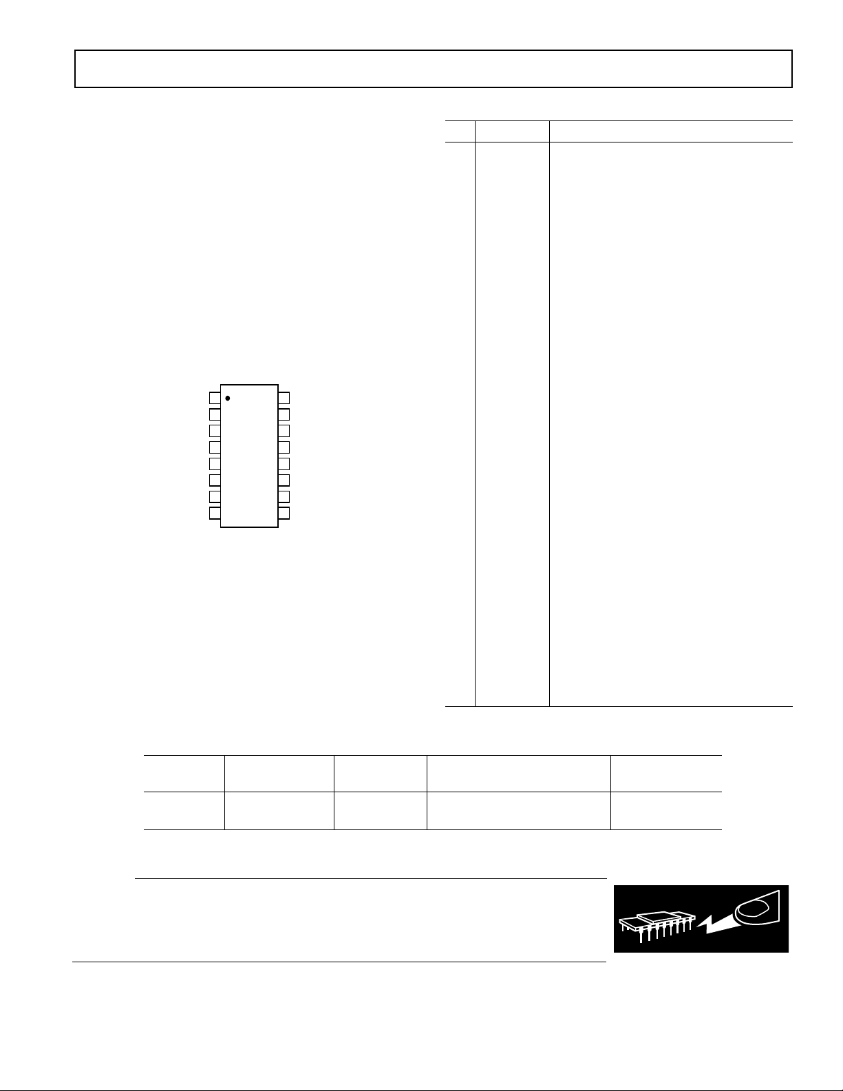
PIN CONFIGURATION
VID0
VID1
VID2
VID3
LRFB1
LRDRV1
CS–
CS+
1
2
3
ADP3158/
ADP3178
4
TOP VIEW
5
(Not to Scale)
6
7
8
16
15
14
13
12
11
10
9
GND
DRVH
DRVL
VCC
LRFB2
LRDRV2
COMP
CT
PIN FUNCTION DESCRIPTIONS
Pin Mnemonic Function
1–4 VID0–VID3 Voltage Identification DAC Inputs.
These pins are pulled up to an internal
reference, providing a Logic 1 if left
open. The DAC output programs the CS–
regulation voltage from 1.3 V to 2.05 V.
5, 12 LRFB1, Feedback connections for the linear
LRFB2 regulator controllers.
6, 11 LRDRV1, Gate drives for the respective linear
LRDRV2 regulator N-channel MOSFETs.
7 CS– Current Sense Negative Node. Negative
input for the current comparator. This pin
also connects to the internal error amplifier that senses the output voltage.
8 CS+ Current Sense Positive Node. Positive
input for the current comparator. The
output current is sensed as a voltage at this
pin with respect to CS–.
9 CT External capacitor connected from CT to
ground sets the Off-time of the device.
10 COMP Error Amplifier Output and Compensation
Point. The voltage at this output programs
the output current control level between
CS+ and CS–.
13 VCC Supply Voltage for the device.
14 DRVL Low-Side MOSFET Drive. Gate drive for
the synchronous rectifier N-channel
MOSFET. The voltage at DRVL swings
from GND to VCC.
15 DRVH High-Side MOSFET Drive. Gate drive
for the buck switch N-channel MOSFET.
The voltage at DRVH swings from GND
to VCC.
16 GND Ground Reference. GND should have a
low impedance path to the source of the
synchronous MOSFET.
ORDERING GUIDE
Temperature LDO Package Package
Model Range Voltage Description Option
ADP3158JR 0°C to 70°C 2.5 V, 1.8 V SO = Small Outline Package R-16A (SO-16)
ADP3178JR 0°C to 70°C Adjustable SO = Small Outline Package R-16A (SO-16)
CAUTION
ESD (electrostatic discharge) sensitive device. Electrostatic charges as high as 4000 V readily
accumulate on the human body and test equipment and can discharge without detection. Although
the ADP3158/ADP3178 feature proprietary ESD protection circuitry, permanent damage may
occur on devices subjected to high-energy electrostatic discharges. Therefore, proper ESD precautions
are recommended to avoid performance degradation or loss of functionality.
REV. A
–3–
Page 4
ADP3158/ADP3178
–Typical Performance Characteristics
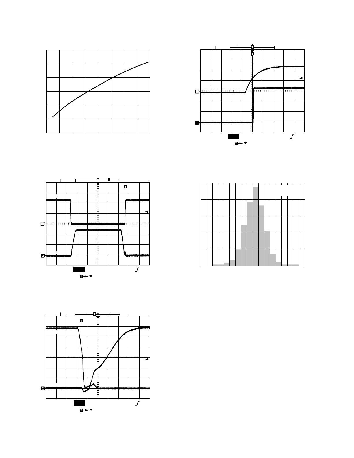
60
50
40
30
20
SUPPLY CURRENT – mA
10
0
0 100 200 300 400 500 600 700 800
OSCILLATOR FREQUENCY – kHz
TPC 1. Supply Current vs. Operating Frequency Using
MOSFETs of Figure 3
TEK RUN TRIG'D
DRVH
TEK RUN TRIG'D
VCC
1
V
CORE
2
CH1
5.00V CH2 500mV BW M 10.0ms A CH1
W
0.00000 s
TPC 4. Power-On Start-Up Waveform
25
20
TA = 25C
V
= 1.65V
OUT
5.90VB
1
DRVL
CH1
5.00V CH2 5.00V BW M 1.00s A CH1
W
–2.6500s
5.90VB
TPC 2. Gate Switching Waveforms Using MOSFETs of
Figure 3
TEK RUN TRIG'D
DRVH
DRVL
15
10
NUMBER OF PARTS – %
5
0
–0.5
OUTPUT ACCURACY – % of Nominal
0 0.5
TPC 5. Output Accuracy Distribution
CH1
2.00V CH2 2.00V BW M 1.00ns A
W
150.000s
CH1
5.88VB
TPC 3. Driver Transition Waveforms Using MOSFETs of
Figure 3
–4–
REV. A
Page 5
ADP3158/ADP3178
ADP3158/
ADP3178
4-BIT CODE
V
CS–
1
VID0
2
VID1
3
VID2
4
VID3
5
LRFB1
6
LRDRV1
7
CS–
8
CS+
GND
DRVH
DRVL
VCC
LRFB2
LRDRV2
COMP
16
15
14
13
+
1F
12
11
10
9
CT
1.2V
+
AD820
12V
100nF
100
100nF
Figure 1. Closed Loop Output Voltage Accuracy
Test Circuit
ADP3158/
ADP3178
1
VID0
2
VID1
3
VID2
4
VID3
V
LR1
10nF
5
LRFB1
6
LRDRV1
7
CS–
8
CS+
GND
DRVH
DRVL
VCC
LRFB2
LRDRV2
COMP
CT
16
15
14
13
12
11
10
9
+
10nF
1F
V
LR2
VCC
100nF
Figure 2. Linear Regulator Output Voltage Accuracy
Test Circuit
THEORY OF OPERATION
The ADP3158 and ADP3178 use a current-mode, constant offtime control technique to switch a pair of external N-channel
MOSFETs in a synchronous buck topology. Constant off-time
operation offers several performance advantages, including that
no slope compensation is required for stable operation. A unique
feature of the constant off-time control technique is that since
the off-time is fixed, the converter’s switching frequency is a
function of the ratio of input voltage to output voltage. The
fixed off-time is programmed by the value of an external capacitor connected to the CT pin. The on-time varies in such a way
that a regulated output voltage is maintained as described below
in the cycle-by-cycle operation. The on-time does not vary under
fixed input supply conditions, and it varies only slightly as a
function of load. This means that the switching frequency remains
fairly constant in a standard computer application.
Active Voltage Positioning
The output voltage is sensed at the CS– pin. A voltage error
amplifier, (g
), amplifies the difference between the output
m
voltage and a programmable reference voltage. The reference
voltage is programmed to between 1.3 V and 2.05 V by an internal 4-bit DAC that reads the code at the voltage identification
(VID) pins. (Refer to Table I for output voltage vs. VID pin code
information.) A unique supplemental regulation technique called
Analog Devices Optimal Positioning Technology (ADOPT)
adjusts the output voltage as a function of the load current so it
is always optimally positioned for a load transient. Standard
(passive) voltage positioning, sometimes recommended for use
with other architectures, has poor dynamic performance which
renders it ineffective under the stringent repetitive transient
conditions specified in Intel VRM documents. Consequently,
such techniques do not allow the minimum possible number of
output capacitors to be used. ADOPT, as used in the ADP3158
and ADP3178, provides a bandwidth for transient response that
is limited only by parasitic output inductance. This yields optimal load transient response with the minimum number of output
capacitors.
Cycle-by-Cycle Operation
During normal operation (when the output voltage is regulated),
the voltage error amplifier and the current comparator are the
main control elements. During the on-time of the high-side
MOSFET, the current comparator monitors the voltage between
the CS+ and CS– pins. When the voltage level between the two
pins reaches the threshold level, the DRVH output is switched
to ground, which turns off the high-side MOSFET. The timing
capacitor CT is then charged at a rate determined by the offtime controller. While the timing capacitor is charging, the DRVL
output goes high, turning on the low-side MOSFET. When the
voltage level on the timing capacitor has charged to the upper
threshold voltage level, a comparator resets a latch. The output
of the latch forces the low-side drive output to go low and the
high-side drive output to go high. As a result, the low-side switch
is turned off and the high-side switch is turned on. The sequence
is then repeated. As the load current increases, the output voltage
starts to decrease. This causes an increase in the output of the
voltage-error amplifier, which, in turn, leads to an increase in
the current comparator threshold, thus tracking the load current. To prevent cross conduction of the external MOSFETs,
feedback is incorporated to sense the state of the driver output
pins. Before the low-side drive output can go high, the high-side
drive output must be low. Likewise, the high-side drive output is
unable to go high while the low-side drive output is high.
Output Crowbar
An added feature of using an N-channel MOSFET as the synchronous switch is the ability to crowbar the output with the
same MOSFET. If the output voltage is 20% greater than the
targeted value, the controller IC will turn on the lower MOSFET,
which will current-limit the source power supply or blow its fuse,
pull down the output voltage, and thus save the microprocessor
from destruction. The crowbar function releases at approximately 50% of the nominal output voltage. For example, if the
output is programmed to 1.5 V, but is pulled up to 1.85 V or
above, the crowbar will turn on the lower MOSFET. If in this
case the output is pulled down to less than 0.75 V, the crowbar
will release, allowing the output voltage to recover to 1.5 V if
the fault condition has been removed.
On-board Linear Regulator Controllers
The ADP3158 and ADP3178 include two linear regulator controllers to provide a low cost solution for generating additional
supply rails. In the ADP3158, these regulators are internally set
to 2.5 V (LR1) and 1.8 V (LR2) with ±2.5% accuracy. The
ADP3178 is designed to allow the outputs to be set externally
using a resistor divider. The output voltage is sensed by the high
input impedance LRFB(x) pin and compared to an internal
fixed reference.
The LRDRV(x) pin controls the gate of an external N-channel
MOSFET resulting in a negative feedback loop. The only additional components required are a capacitor and resistor for
stability. The maximum output load current is determined by
the size and thermal impedance of the external power MOSFET
that is placed in series with the supply.
REV. A
–5–
Page 6

ADP3158/ADP3178
FROM CPU
3.3V
C15
1F
Q1
100F
*
+
C1
V
LR1
2.5V, 2A
10k
R2
C2
68pF
1
2
3
4
5
6
7
8
C10
1nF
VID0
VID1
VID2
VID3
LRFB1
LRDRV1
CS–
CS+
ADP3158/
ADP3178
U1
LRFB2
LRDRV2
COMP
R4
220
GND
DRVH
DRVL
VCC
CT
220
16
15
14
13
12
11
10
150pF
R3
D2
MBR052LT1
D3
MBR052LT1
+
C6
1F
L1
1.7H
R11
10k
V
1.8V,
2A
LR2
C8
1000F
R12
4m
C17 C18 C19 C20 C21
C7
22F
*
Q4
Q3
**
C11
3.3V
68pF
R
A
10.5k
78.7k
C
R
OC
B
2.7nF
9
C3
Q2
+
C2
100F
C12
1F
*
L2
1H
+++
C9
1000F
1000F 5
24m (EACH)
*
SUB45N03-13L
**
SUB75N03-07
5V STANDBY
12V
5V
VCC CORE
1.30V TO
2.05V
+++++
15A
Figure 3. 15 A Pentium III Application Circuit
The linear regulator controllers have been designed so that they
remain active even when the switching controller is in UVLO mode
to ensure that the output voltages of the linear regulators will track
the 3.3 V supply as required by Intel design specifications. By
diode ORing the VCC input of the IC to the 5 VSB and 12 V
supplies as shown in Figure 3, the switching output will be disabled
in standby mode, but the linear regulators will begin conducting
once VCC rises above about 1 V. During start-up the linear outputs will track the 3.3 V supply up until they reach their respective
regulation points, regardless of the state of the 12 V supply. Once
the 12 V supply has exceeded the 5 VSB supply by more than a
diode drop, the controller IC will track the 12 V supply. Once the
12 V supply has risen above the UVLO value, the switching regulator will begin its start-up sequence.
Table I. Output Voltage vs. VID Code
VID3 VID2 VID1 VID0 V
OUT(NOM)
1 1 1 1 1.30 V
1 1 1 0 1.35 V
1 1 0 1 1.40 V
1 1 0 0 1.45 V
1 0 1 1 1.50 V
1 0 1 0 1.55 V
1 0 0 1 1.60 V
1 0 0 0 1.65 V
0 1 1 1 1.70 V
0 1 1 0 1.75 V
0 1 0 1 1.80 V
0 1 0 0 1.85 V
0 0 1 1 1.90 V
0 0 1 0 1.95 V
0 0 0 1 2.00 V
0 0 0 0 2.05 V
APPLICATION INFORMATION
Specifications for a Design Example
The design parameters for a typical 750 MHz Pentium III application (shown in Figure 3) are as follows:
Input Voltage: (V
Auxiliary Input: (V
Output Voltage (V
Maximum Output Current (I
Minimum Output Current (I
) = 5 V
IN
) = 12 V
CC
) = 1.7 V
VID
O(MAX)
O(MIN)
) = 15 A
) = 1 A
Static tolerance of the supply voltage for the processor core
(∆V
) = +40 mV (–80 mV) = 120 mV
O
Transient tolerance (for less than 2 µs) of the supply voltage
for the processor core when the load changes between the
minimum and maximum values with a di/dt of 20 A/µs
(∆V
O(TRANSIENT)
) = +80 mV (–130 mV) = 210 mV
Input current di/dt when the load changes between the minimum and maximum values < 0.1 A/µs.
The above requirements correspond to Intel’s published power
supply requirements based on VRM 8.4 guidelines.
–6–
REV. A
Page 7

ADP3158/ADP3178
CT Selection for Operating Frequency
The ADP3158 and ADP3178 use a constant off-time architecture
with t
determined by an external timing capacitor CT. Each
OFF
time the high-side N-channel MOSFET switch turns on, the voltage across CT is reset to 0 V. During the off-time, CT is charged
by a constant current of 150 µA. Once CT reaches 3.0 V, a new
on-time cycle is initiated. The value of the off-time is calculated
using the continuous-mode operating frequency. Assuming a
nominal operating frequency (f
) of 200 kHz at an output volt-
NOM
age of 1.7 V, the corresponding off-time is:
t
OFF
t
OFF
1
=
1
=−
V
OUT
–
×
Vf
IN NOM
17
.
V
×=
5
200
V kHz
1
1
33
. µ
s
(1)
The timing capacitor can be calculated from the equation:
tIVsA
×
OFF CT
C
=
T
TTH
()
.3 3 150
=
µ× µ
V
3
≈
150
pF
(2)
(3)
f
=×
MIN
VI R R RV
1
t
OFF
– ()–
IN O MAX DS ON HSF SENSE L OUT
VI R R RR
– ( – )
IN O MAX DS ON HSF SENSE L DS ON LSF
( ) () ())
×++
() ()
×++
The converter only operates at the nominal operating frequency
at the above-specified V
of V
, or under heavy load, the operating frequency decreases
OUT
and at light load. At higher values
OUT
due to the parasitic voltage drops across the power devices. The
actual minimum frequency at V
= 1.7 V is calculated to be
OUT
195 kHz (see Equation 3), where:
R
DS(ON)HSF
is the resistance of the high-side MOSFET
(estimated value: 14 mΩ)
R
DS(ON)LSF
is the resistance of the low-side MOSFET
(estimated value: 6 mΩ)
R
is the resistance of the sense resistor
SENSE
(estimated value: 4 mΩ)
R
is the resistance of the inductor
L
(estimated value: 3 mΩ)
Inductance Selection
The choice of inductance determines the ripple current in the
inductor. Less inductance leads to more ripple current, which
increases the output ripple voltage and the conduction losses in
the MOSFETs, but allows using smaller-size inductors and, for
a specified peak-to-peak transient deviation, output capacitors
with less total capacitance. Conversely, a higher inductance means
lower ripple current and reduced conduction losses, but requires
larger-size inductors and more output capacitance for the same
peak-to-peak transient deviation. The following equation shows
the relationship between the inductance, oscillator frequency,
peak-to-peak ripple current in an inductor and input and
output voltages.
Vt
×
OUT OFF
L
=
I
L RIPPLE
()
(4)
For 4 A peak-to-peak ripple current, which corresponds to
approximately 25% of the 15 A full-load dc current in an inductor,
Equation 4 yields an inductance of
L
A
4
H=
=µ
14
.
Vs
×µ
17 33
..
A 1.5 µH inductor can be used, which gives a calculated ripple
current of 3.8 A at no load. The inductor should not saturate at
the peak current of 17 A and should be able to handle the sum
of the power dissipation caused by the average current of 15 A
in the winding and the core loss.
Designing an Inductor
Once the inductance is known, the next step is either to design an
inductor or find a standard inductor that comes as close as
possible to meeting the overall design goals. The first decision
in designing the inductor is to choose the core material. There
are several possibilities for providing low core loss at high frequencies. Two examples are the powder cores (e.g., Kool-Mµ
®
from
Magnetics, Inc.) and the gapped soft ferrite cores (e.g., 3F3 or 3F4
from Philips). Low frequency powdered iron cores should be
avoided due to their high core loss, especially when the inductor
value is relatively low and the ripple current is high.
Two main core types can be used in this application. Open
magnetic loop types, such as beads, beads on leads, and rods
and slugs, provide lower cost but do not have a focused magnetic field in the core. The radiated EMI from the distributed
magnetic field may create problems with noise interference in
the circuitry surrounding the inductor. Closed-loop types, such
as pot cores, PQ, U, and E cores, or toroids, cost more, but
have much better EMI/RFI performance. A good compromise
between price and performance are cores with a toroidal shape.
REV. A
–7–
Page 8

ADP3158/ADP3178
There are many useful references for quickly designing a power
inductor. Table II gives some examples.
Table II. Magnetics Design References
Magnetic Designer Software
Intusoft (http://www.intusoft.com)
Designing Magnetic Components for High-Frequency DC-DC
Converters
McLyman, Kg Magnetics
ISBN 1-883107-00-08
Selecting a Standard Inductor
The companies listed in Table III can provide design consultation and deliver power inductors optimized for high power
applications upon request.
Table III. Power Inductor Manufacturers
Coilcraft
(847) 639-6400
http://www.coilcraft.com
Coiltronics
(561) 752-5000
http://www.coiltronics.com
Sumida Electric Company
(408) 982-9660
http://www.sumida.com
C
Selection—Determining the ESR
OUT
The required equivalent series resistance (ESR) and capacitance
drive the selection of the type and quantity of the output capacitors. The ESR must be small enough to contain the voltage
deviation caused by a maximum allowable CPU transient current within the specified voltage limits, giving consideration also
to the output ripple and the regulation tolerance. The capacitance must be large enough that the voltage across the capacitor,
which is the sum of the resistive and capacitive voltage deviations,
does not deviate beyond the initial resistive deviation while the
inductor current ramps up or down to the value corresponding
to the new load current. The maximum allowed ESR also represents the maximum allowed output resistance, R
OUT
.
The cumulative errors in the output voltage regulation cuts into
the available regulation window, V
. When considering dynamic
WIN
load regulation this relates directly to the ESR. When considering dc load regulation, this relates directly to the programmed
output resistance of the power converter.
Some error sources, such as initial voltage accuracy and ripple
voltage, can be directly deducted from the available regulation
window, while other error sources scale proportionally to the
amount of voltage positioning used, which, for an optimal design,
should utilize the maximum that the regulation window will allow.
The error determination is a closed-loop calculation, but it can
be closely approximated. To maintain a conservative design while
avoiding an impractical design, various error sources should
be considered and summed statistically.
The output ripple voltage can be factored into the calculation by
summing the output ripple current with the maximum output
current to determine an effective maximum dynamic current
change. The remaining errors are summed separately according
to the formula:
VVV k
=××
( – )
WIN VID VID
∆
2
(5)
where k
I
O
1
–
II
+
OO
∆
= 0.5% is the initial programmed voltage tolerance
VID
2
k
+
RCS
from the graph of TPC 6, k
current sense resistor, k
CSF
the current sense filter components, k
the two termination resistors added at the COMP pin, and k
2
k
CSF
2
= 2% is the tolerance of the
RCS
22
kk mV
++
RT EA
95
=
= 10% is the summed tolerance of
= 2% is the tolerance of
RT
EA
= 8% accounts for the IC current loop gain tolerance including
the g
tolerance.
m
The remaining window is then divided by the maximum output
current plus the ripple to determine the maximum allowed ESR
and output resistance:
RR
==+=
E MAX OUT MAX
() ()
V
WIN
IImVAA
OO
15 3 8
∆
95
m
Ω
5
=
.
+
(6)
The output filter capacitor bank must have an ESR of less
than 5 mΩ. One can, for example, use five ZA series capacitors
from Rubycon which would give an ESR of 4.8 mΩ. Without
ADOPT voltage positioning, the ESR would need to be less than
3 mΩ, yielding a 50% increase to eight Rubycon output capacitors.
C
— Checking the Capacitance
OUT
As long as the capacitance of the output capacitor is above a
critical value and the regulating loop is compensated with ADOPT,
the actual value has no influence on the peak-to-peak deviation
of the output voltage to a full step change in the load current.
The critical capacitance can be calculated as follows:
I
C
OUT CRIT
()
A
15
=
m
.
Ω×
517
O
=
RV
×
EOUT
..
×µ=
15 26
×
HmF
L
(7)
The critical capacitance for the five ZA series Rubycon capacitors is 2.6 mF while the equivalent capacitance is 5 mF. The
capacitance is safely above the critical value.
–8–
REV. A
Page 9

ADP3158/ADP3178
R
SENSE
The value of R
is based on the maximum required output
SENSE
current. The current comparators of the ADP3158 and ADP3178
have a minimum current limit threshold of 69 mV. Note that the
69 mV value cannot be used for the maximum specified nominal
current, as headroom is needed for ripple current and tolerances.
The current comparator threshold sets the peak of the inductor
current yielding a maximum output current, IO, which equals twice
the peak inductor current value less half of the peak-to-peak inductor ripple current. From this the maximum value of R
SENSE
is
calculated as:
R
SENSE
≤
I
V
CS CL MIN
()( )
I
L RIPPLE
+
O
()
=
2
mV
69
AA
+
15 1 9
.
m
=Ω
4
(8)
In this case, 4 mΩ was chosen as the closest standard value.
Once R
where current limit is reached, I
has been chosen, the output current at the point
SENSE
, can be calculated using
OUT(CL)
the maximum current sense threshold of 87 mV:
I
OUT CL
()
87
=
4
V
CS CL MAX
()( ) ( )
=
R
SENSE
mV
m
.
38
–
Ω
I
L RIPPLE
–
2
A
2
A
≈
20
(9)
At output voltages below 450 mV, the current sense threshold is
reduced to 54 mV, and the ripple current is negligible. Therefore, at dead short the output current is reduced to:
mV
I
OUT SC()
54
A
.=
=
13 5
m
Ω
4
(10)
To safely carry the current under maximum load conditions, the
sense resistor must have a power rating of at least:
PIR AmW
R O SENSE
SENSE
22
=× = ×Ω=() ( ) .
20 4 1 6
(11)
Power MOSFETs
Two external N-channel power MOSFETs must be selected for
use with the ADP3158 and ADP3178, one for the main switch
and an identical one for the synchronous switch. The main
selection parameters for the power MOSFETs are the threshold
voltage (V
) and the ON-resistance (R
GS(TH)
DS(ON)
).
The minimum input voltage dictates whether standard threshold
or logic-level threshold MOSFETs must be used. For V
standard threshold MOSFETs (V
< 4 V) may be used. If
GS(TH)
> 8 V,
IN
V
is expected to drop below 8 V, logic-level threshold MOSFETs
IN
(V
MOSFETs with V
value of V
The maximum output current I
< 2.5 V) are strongly recommended. Only logic-level
GS(TH)
should be used.
CC
ratings higher than the absolute maximum
GS
determines the R
O(MAX)
DS(ON)
requirement for the two power MOSFETs. When the ADP3158
and ADP3178 are operating in continuous mode, the simplifying
assumption can be made that one of the two MOSFETs is always
conducting the average load current. For V
IN
= 5 V and V
OUT
=
1.65 V, the maximum duty ratio of the high-side FET is:
Dft
HSF MAX MIN OFF
()
D kHz s
HSF MAX
()
–()
=×
1
–(.)%
=×µ=
1 195 3 3 36
(12)
The maximum duty ratio of the low-side (synchronous rectifier)
MOSFET is:
DD
LSF MAX HSF MAX() ()
– %==154
(13)
The maximum rms current of the high-side MOSFET is:
ID
=×
RMSHSF HSF MAX
I
RMSHSF
()
13 1 13 1 16 1 16 1
36
=×
%
IIII
AAAA
.(. .).
22
+×+
L VALLEY L VALLEY L PEAK L PEAK
()()()()
22
+×+
()
3
(14)
88
A rms
=
3
.
The maximum rms current of the low-side MOSFET is:
ID
=×
RMSLSF LSF MAX
I
RMSLSF
The R
DS(ON)
()
13 1 13 1 16 1 16 1
54
%
=×
for each MOSFET can be derived from the allowable
IIII
.(. .).
AAAA
22
L VALLEY L VALLEY L PEAK L PEAK
22
+×+
()()()()
+×+
3
3
(15)
10 8
.
A rms
=
dissipation. If 10% of the maximum output power is allowed for
MOSFET dissipation, the total dissipation will be:
PVI W
D FETs OUT OUT MAX() ( )
..=× × =01 226
(16)
Allocating half of the total dissipation for the high-side MOSFET
and half for the low-side MOSFET and assuming that switching
losses are small relative to the dc conduction losses, the required
minimum MOSFET resistances will be:
R
DS ON HSF
()
R
DS ON LSF
()
P
HSF
≤= =Ω
22
I
HSF
P
LSF
≤= =Ω
22
I
LSF
.
113
.
88
.
113
.
10 8
W
A
W
A
10
15
m
m
(17)
(18)
REV. A
–9–
Page 10

ADP3158/ADP3178
Note that there is a trade-off between converter efficiency and
cost. Larger MOSFETs reduce the conduction losses and allow
higher efficiency, but increase the system cost. If efficiency is not a
major concern, a Vishay-Siliconix SUB45N03-13L (R
DS(ON)
=
10 mΩ nominal, 16 mΩ worst-case) for the high-side and a
Vishay-Siliconix SUB75N03-07 (R
= 6 mΩ nominal,
DS(ON)
10 mΩ worst-case) for the low-side are good choices.
The high-side MOSFET dissipation is:
VI Qf
PI R
=×+
DHSF RMSHSF DS ON
PAm
=×Ω+
DHSF
2
()
2
88 16
..
×××
IN L PEAK G MIN
()
I
×
2
G
V A nC kHz
×× ×
5 15 70 195
A
×
21
=
175
(19)
W
where the second term represents the turn-off loss of the
MOSFET. In the second term, Q
removed from the gate for turn-off and I
From the data sheet, Q
is 70 nC and the gate drive current
G
is the gate charge to be
G
is the gate current.
G
provided by the ADP3159 is about 1 A.
The low-side MOSFET dissipation is:
PI R
=×
DLSF RMSLSF DS ON
PAmW
10 8 10 1 08
=×Ω=
DLSF
2
()
2
..
(20)
Note that there are no switching losses in the low-side MOSFET.
Surface mount MOSFETs are preferred in CPU core converter
applications due to their ability to be handled by automatic
assembly equipment. The TO-263 package offers the power
handling of a TO-220 in a surface-mount package. However,
this package still needs adequate copper area on the PCB to
help move the heat away from the package.
The junction temperature for a given area of 2-ounce copper
can be approximated using:
TPT
=×
()
AD AJJ
+θ
(21)
assuming:
θ
= 45°C/W for 0.5 in
JA
θJA = 36°C/W for 1 in
θJA = 28°C/W for 2 in
2
2
2
For 1 in2 of copper area attached to each transistor and an
ambient temperature of 50°C:
T
= (36°C/W × 1.48 W) + 50°C = 103°C
JHSF
T
= (36°C/W × 1.08 W) + 50°C = 89°C
JLSF
All of the above-calculated junction temperatures are safely
below the 175°C maximum specified junction temperature of
the selected MOSFETs.
CIN Selection and Input Current di/dt Reduction
In continuous inductor-current mode, the source current of the
high-side MOSFET is approximately a square wave with a duty
ratio equal to V
OUT/VIN
and an amplitude of one-half of the
maximum output current. To prevent large voltage transients, a
low ESR input capacitor sized for the maximum rms current
must be used. The maximum rms capacitor current is given by:
IIDD
=−=
C RMS O HSF HSF()
2
(22)
AA
15 0 36 0 36 7 2
. – ..
2
=
For a ZA-type capacitor with 1000 µF capacitance and 6.3 V
voltage rating, the ESR is 24 mΩ and the maximum allowable
ripple current at 100 kHz is 2 A. At 105°C, at least four such
capacitors must be connected in parallel to handle the calculated
ripple current. At 50°C ambient, however, a higher ripple current can be tolerated, so three capacitors in parallel are adequate.
The ripple voltage across the three paralleled capacitors is:
ESR
()
VI
()
C IN RIPPLE O
VA
()
C IN RIPPLE
=× +
=×Ω+
CIN
n
24
nC f
C
m
3363 1000 195
D
HSF
××
C IN MAX
×µ×
%
FkHz
=15
129
mV
(23)
To further reduce the effect of the ripple voltage on the system
supply voltage bus, and to reduce the input-current di/dt to
below the recommended maximum of 0.1 A/ms, an additional
small inductor (L > 1 µH @ 10 A) should be inserted between
the converter and the supply bus.
Feedback Compensation for Active Voltage Positioning
Optimized compensation of the ADP3158 and ADP3178 allows
the best possible containment of the peak-to-peak output voltage
deviation. Any practical switching power converter is inherently
limited by the inductor in its output current slew rate to a value
much less than the slew rate of the load. Therefore, any sudden
change of load current will initially flow through the output capacitors, and this will produce an output voltage deviation equal to the
ESR of the output capacitor array times the load current change.
TEK RUN: 200kS/s SAMPLE
2
CH1 M 250s CH2 680mV
100mV
TRIG'D
CH2
Figure 4. Transient Response of the Circuit of Figure 3
–10–
REV. A
Page 11

ADP3158/ADP3178
100
90
80
70
60
50
40
EFFICIENCY – %
30
20
10
0
0
2
468101214161820
OUTPUT CURRENT – A
Figure 5. Efficiency vs. Load Current of the Circuit
of Figure 3
To correctly implement active voltage positioning, the low frequency output impedance (i.e., the output resistance) of the
converter should be made equal to the maximum ESR of the
output capacitor array. This can be achieved by having a singlepole roll-off of the voltage gain of the g
error amplifier, where
m
the pole frequency coincides with the ESR zero of the output
capacitor. A gain with single-pole roll-off requires that the g
m
amplifier output pin be terminated by the parallel combination
of a resistor and capacitor. The required resistor value can be
calculated from the equation:
RR
×
R
where:
R
COMP
TOTAL
OGM TOTAL
=
RR
–
OGM TOTAL
nR
×
I SENSE
=
gR
×
()
E MAX
m
In Equations 24 and 25, R
OGM
Mk
Ω× Ω
191
=
Mk
191
25 4
=
mmho m
.
22 5
.
=Ω
.
ΩΩ
– .
m
×Ω
×Ω
92
=Ω
.
91
k
k
is the internal resistance of the g
(24)
(25)
m
amplifier, nI is the division ratio from the output voltage to
signal of the g
transconductance of the g
Although a single termination resistor equal to R
amplifier to the PWM comparator, and gm is the
m
amplifier itself.
m
would yield
COMP
the proper voltage positioning gain, the dc biasing of that resistor
would determine how the regulation band is centered (i.e., offset).
Note that sometimes the specified regulation band is asymmetrical
with respect to the nominal VID voltage. With the ADP3158 and
ADP3178, the offset is already considered part of the design
procedure—no special provision is required. To accomplish the dc
biasing, it is simplest to use two resistors to terminate the g
m
amplifier output, with the lower resistor (RB) tied to ground and
the upper resistor (R
) to the 12 V supply of the IC. The values of
A
these resistors can be calculated using:
R
=
A
V
gV K
×+
()
OUT OS
m
DIV
()
=
mmho mV
.( .)
22 22 47 10
V
12
×+×
–
2
k
=Ω
.
79 1
(26)
where K is a constant determined by internal characteristics of the
ADP3158 and ADP3178, peak-to-peak inductor current ripple
), and the current sampling resistor (R
(I
RIPPLE
calculated using Equations 28 and 29. V
DIV
supply voltage (e.g., the recommended 12 V supply) and V
). K can be
SENSE
is the resistor divider
is
OUT(OS)
the output voltage offset from the nominal VID-programmed value
under no load condition. This offset is given by Equation 30.
The closest 1% value for R
to solve for R
RR
R
=
B
RR
:
B
×
A COMP
–
A COMP
=
The nearest 1% value of 10.5 kΩ was chosen for R
I
L RIPPLE
()
K
=×
()
Rn
22
SENSE I
gRVgR
×
m TOTAL
is 78.7 kΩ. This value is then used
A
kk
Ω× Ω
..
78 7 9 2
kk
ΩΩ
. – .
78 7 9 2
×
GNL
+
××
m TOTAL
–
k
=Ω
.
10 4
V
CC
gR
m OGM
(27)
.
B
(28)
.
38
Am
K
=×
2
2
–
.
47 10
=×
VV
=+
GNL GNL
425
Ω×
..... .
22 91
mmho k mmho k
IRn
L RIPPLE SENSE I
()
0
+
×Ω
22 91122 2 2 130
××
2
1 174
×Ω−××Ω
VV
−
IN VID
−
L
V
mmho k
×× ×
tR n
D SENSE I
(29)
×Ω×
. – .
38 4 252517
=+
1
VV
GNL
VV V
OUT OS OUT MAX VID
() ( )
VmV
OUT OS
()
Am V V
=−
()
mA
=−
40
538
−
RI
−
Ω×
.
2
××Ω×
75 4 25 1 174
µ
.
15
E MAX L RIPPLE
()( )
ns m V
H
×
2
3
VmV
−××=
17 5 10 22
.
–
=
Vk
−×
VID VID
.
(30)
Finally, the compensating capacitance is determined from the
equality of the pole frequency of the error amplifier gain and the
zero frequency of the impedance of the output capacitor:
C ESRRmF m
OC
OUT
=
TOTAL
=
C
×
The closest standard value for C
×Ω
548
91
.
.
k
Ω
is 2.7 nF.
OC
=
26
.
nF
(31)
REV. A
–11–
Page 12

ADP3158/ADP3178
Trade-Offs Between DC Load Regulation and AC Load
Regulation
Casual observation of the circuit operation—e.g., with a voltmeter
—would make it appear that the dc load regulation appears to
be rather poor compared to a conventional regulator (see Figure
4). This would be especially noticeable under very light or very
heavy loads where the voltage is “positioned” near one of the
extremes of the regulation window rather than near the nominal
center value. It must be noted and understood that this low gain
characteristic (i.e., loose dc load regulation) is inherently required
to allow improved transient containment (i.e., to achieve tighter
ac load regulation). That is, the dc load regulation is intentionally
sacrificed (but kept within specification) in order to minimize
the number of capacitors required to contain the load transients
produced by the CPU.
3.3V
ADP3158/
ADP3178
LRDRV1
LRFB1
2.5V
V
LR2
2.5V, 2.2A
1F
R
250m
100F
S
10k
1k
68pF
Figure 6. Adding Overcurrent Protection to the
Linear Regulator
Linear Regulators
The two linear regulators provide a low cost, convenient, and
versatile solution for generating additional supply rails. The
maximum output load current is determined by the size and
thermal impedance of the external N-channel power MOSFET
that is placed in series with the supply. The output voltage is
sensed at the LRFB pin and compared to an internal reference
voltage in a negative feedback loop which keeps the output voltage
in regulation. If the load is reduced or increased, the MOSFET
drive will also be reduced or increased by the controller IC to
provide a well-regulated ±2.5% accurate output voltage.
The LRFB threshold of the ADP3158 are internally set at 2.5 V
(LRFB1) and 1.8 V (LRFB2), while the LRFB pins of the
ADP3178 are compared to an internal 1 V reference. This allows
the use of an external resistor divider network to program the linear
regulator output voltage. The correct resistor values for setting the
output voltage of the linear regulators in the ADP3178 can be
determined using:
RR
+
VV
OUT LR LRFB
=×
()
Assuming that R
= 10 kΩ, V
L
Equation 32 to solve for R
UL
R
L
OUT(LR)
yields:
U
(32)
= 1.2 V and rearranging
Efficiency of the Linear Regulators
The efficiency and corresponding power dissipation of each
of the linear regulators are not determined by the controller
IC. Rather, these are a function of input and output voltage and
load current. Efficiency is approximated by the formula:
V
η= ×100%
V
OUT
IN
(34)
The corresponding power dissipation in the MOSFET, together
with any resistance added in series from input to output, is given by:
PVVI
=×( – )
LDO IN OUT OUT
(35)
Minimum power dissipation and maximum efficiency are accomplished by choosing the lowest available input voltage that exceeds
the desired output voltage. However, if the chosen input source
is itself generated by a linear regulator, its power dissipation will
be increased in proportion to the additional current it must
now provide.
Implementing Current Limit for the Linear Regulators
The circuit of Figure 4 gives an example of a current limit protection circuit that can be used in conjunction with the linear
regulators. The output voltage is internally set by the LRFB
pin. The value of the current sense resistor may be calculated
as follows:
mV
540 540
R
≅==Ω
S
I
O MAX
()
22
.
mV
A
250
m
(36)
The power rating of the current sense resistor must be at least:
PRI W
DR
S
SOMAX() ( )
.=× =212
(37)
The maximum linear regulator MOSFET junction temperature
with a shorted output is:
TT VI
MAX A C IN O MAX
JJ
() ()
TCCWVAC
MAX
J
()
()
=+ × ×
θ
=°+ ° × × =°
(. / (. . )
50 14 33 22 60
(38)
which is within the maximum allowed by the MOSFET’s data
sheet specification. The maximum MOSFET junction temperature at nominal output is:
TT VVI
NOM A C IN OUT O NOM
JJ
() ()
TCCWVVAC
NOM
J
()
((– ))
=+ × ×
θ
=°+ ° × × = °
(. / (. – .) )
50 14 33 25 2 52
(39)
This example assumes an infinite heatsink. The practical limitation will be based on the actual heatsink used.
kV V
10
R
=
U
kVV
10 1 2 1
R
=
U
×−
Ω
()
()
OUT LR LRFB
V
LRFB
.
×−
Ω
()
V
1
k
=
2
Ω
(33)
–12–
REV. A
Page 13

ADP3158/ADP3178
LAYOUT AND COMPONENT PLACEMENT GUIDELINES
The following guidelines are recommended for optimal performance of a switching regulator in a PC system:
General Recommendations
1. For best results, a four-layer PCB is recommended. This
should allow the needed versatility for control circuitry
interconnections with optimal placement, a signal ground
plane, power planes for both power ground and the input
power (e.g., 5 V), and wide interconnection traces in the
rest of the power delivery current paths.
2. Whenever high currents must be routed between PCB
layers, vias should be used liberally to create several parallel
current paths so that the resistance and inductance introduced by these current paths is minimized and the via
current rating is not exceeded.
3. If critical signal lines (including the voltage and current
sense lines of the controller IC) must cross through power
circuitry, it is best if a ground plane can be interposed
between those signal lines and the traces of the power
circuitry. This serves as a shield to minimize noise injection into the signals at the cost of making signal ground a
bit noisier.
4. The GND pin should connect first to a ceramic bypass
capacitor (on the VCC pin) and then into the power ground
plane. However, the ground plane should not extend under
other signal components, including the controller IC itself.
5. The output capacitors should also be connected as closely
as possible to the load (or connector) that receives the
power (e.g., a microprocessor core). If the load is distributed,
the capacitors should also be distributed, and generally in
proportion to where the load tends to be more dynamic. It
is also advised to keep the planar interconnection path short
(i.e., have input and output capacitors close together).
6. Absolutely avoid crossing any signal lines over the switching
power path loop, described below.
Power Circuitry
7. The switching power path should be routed on the PCB to
encompass the smallest possible area in order to minimize
radiated switching noise energy (i.e., EMI). Failure to take
proper precaution often results in EMI problems for the
entire PC system as well as noise-related operational problems in the power converter control circuitry. The switching
power path is the loop formed by the current path through
the input capacitors, the two FETs, and the power Schottky
diode, if used, including all interconnecting PCB traces and
planes. The use of short and wide interconnection traces is
especially critical in this path for two reasons: it minimizes
the inductance in the switching loop, which can cause highenergy ringing, and it accommodates the high current demand
with minimal voltage loss.
8. A power Schottky diode (1 ~ 2 A dc rating) placed from the
lower MOSFET’s source (anode) to drain (cathode) will
help to minimize switching power dissipation in the upper
MOSFET. In the bñôÖÑx of an effective Schottky diode,
this dissipation occurs through the following sequence of
switching events. The lower MOSFET turns off in advance
of the upper MOSFET turning on (necessary to prevent
cross-conduction). The circulating current in the power
converter, no longer finding a path for current through the
channel of the lower MOSFET, draws current through the
inherent body-drain diode of the MOSFET. The upper
MOSFET turns on, and the reverse recovery characteristic
of the lower MOSFET’s body-drain diode prevents the drain
voltage from being pulled high quickly. The upper MOSFET
then conducts very large current while it momentarily has a
high voltage forced across it, which translates into added
power dissipation in the upper MOSFET. The Schottky diode
minimizes this problem by carrying a majority of the circulating current when the lower MOSFET is turned off, and
by virtue of its essentially nonexistent reverse recovery time.
9. Whenever a power-dissipating component (e.g., a power
MOSFET) is soldered to a PCB, the liberal use of vias,
both directly on the mounting pad and immediately surrounding it, is recommended. Two important reasons for
this are: improved current rating through the vias (if it is a
current path), and improved thermal performance—espe-
cially if the vias extend to the opposite side of the PCB where
a plane can more readily transfer the heat to the air.
10. The output power path, though not as critical as the switching power path, should also be routed to encompass a small
area. The output power path is formed by the current path
through the inductor, the current sensing resistor, the output capacitors, and back to the input capacitors.
11. For best EMI containment, the ground plane should extend
fully under all the power components. These are: the input
capacitors, the power MOSFETs and Schottky diode, the
inductor, the current sense resistor, any snubbing elements
that might be added to dampen ringing, and the output
capacitors.
REV. A
–13–
Page 14

ADP3158/ADP3178
Signal Circuitry
12. The output voltage is sensed and regulated between the
GND pin (which connects to the signal ground plane) and
the CS– pin. The output current is sensed (as a voltage)
and regulated between the CS– pin and the CS+ pin. In
order to avoid differential mode noise pickup in those sensed
signals, their loop areas should be small. Thus the CS–
trace should be routed atop the signal ground plane, and
the CS+ and CS– traces should be routed as a closely
coupled pair (CS+ should be over the signal ground plane
as well).
OUTLINE DIMENSIONS
Dimensions shown in inches and (mm).
16-Lead SOIC
(R-16A/SO-16)
0.3937 (10.00)
0.3859 (9.80)
0.1574 (4.00)
0.1497 (3.80)
16
1
9
0.2440 (6.20)
0.2284 (5.80)
8
13. The CS+ and CS– traces should be Kelvin-connected to
the current sense resistor so that the additional voltage drop
due to current flow on the PCB at the current sense resistor
connections does not affect the sensed voltage. It is desirable to have the controller IC close to the output capacitor
bank and not in the output power path, so that any voltage
drop between the output capacitors and the GND pin is
minimized, and voltage regulation is not compromised.
PIN 1
0.0098 (0.25)
0.0040 (0.10)
0.050 (1.27)
BSC
0.0192 (0.49)
0.0138 (0.35)
0.0688 (1.75)
0.0532 (1.35)
SEATING
PLANE
0.0099 (0.25)
0.0075 (0.19)
0.0196 (0.50)
0.0099 (0.25)
8
0
0.0500 (1.27)
0.0160 (0.41)
45
–14–
REV. A
Page 15

Revision History–ADP3158/ADP3178
Location Page
Global change from ADP3158 to ADP3158/ADP3178
Change from REV. 0 to REV. A.
Edits to GENERAL DESCRIPTION . . . . . . . . . . . . . . . . . . . . . . . . . . . . . . . . . . . . . . . . . . . . . . . . . . . . . . . . . . . . . . . . . . . . . . . 1
Edits to FUNCTIONAL BLOCK DIAGRAM . . . . . . . . . . . . . . . . . . . . . . . . . . . . . . . . . . . . . . . . . . . . . . . . . . . . . . . . . . . . . . . . 1
Edit to ERROR AMPLIFIER section of the SPECIFICATIONS . . . . . . . . . . . . . . . . . . . . . . . . . . . . . . . . . . . . . . . . . . . . . . . . . . 2
Addition to LINEAR REGULATORS section of the SPECIFICATIONS . . . . . . . . . . . . . . . . . . . . . . . . . . . . . . . . . . . . . . . . . . . 2
Addition to ORDERING GUIDE . . . . . . . . . . . . . . . . . . . . . . . . . . . . . . . . . . . . . . . . . . . . . . . . . . . . . . . . . . . . . . . . . . . . . . . . . . 3
Edits to the On-board Linear Regulator Controllers section . . . . . . . . . . . . . . . . . . . . . . . . . . . . . . . . . . . . . . . . . . . . . . . . . . . . . . 5
Edits to Figure 3 . . . . . . . . . . . . . . . . . . . . . . . . . . . . . . . . . . . . . . . . . . . . . . . . . . . . . . . . . . . . . . . . . . . . . . . . . . . . . . . . . . . . . . . 6
Edits to Equations 24, 27, and 31 . . . . . . . . . . . . . . . . . . . . . . . . . . . . . . . . . . . . . . . . . . . . . . . . . . . . . . . . . . . . . . . . . . . . . . . . . 11
Addition of new text to Linear Regulators section . . . . . . . . . . . . . . . . . . . . . . . . . . . . . . . . . . . . . . . . . . . . . . . . . . . . . . . . . . . . . 12
REV. A
–15–
Page 16

C02189–1.5–7/01(A)
–16–
PRINTED IN U.S.A.
 Loading...