

Page 1

Synchronous Buck Controller
a
FEATURES
Fixed 1.2 V N-Channel Synchronous Buck Driver
Two On-Board Linear Regulator Controllers
Total Accuracy ±1% over Temperature
High Efficiency Current-Mode Operation
Short-Circuit Protection
Power Good Output
Overvoltage Protection Crowbar Protects Switching
Output with No Additional External Components
APPLICATIONS
Auxiliary System Supplies for Desktop
Computer Systems
General-Purpose Low Voltage Supplies
with Dual Linear Regulator Controllers
ADP3171
FUNCTIONAL BLOCK DIAGRAM
GND
LRFB1
LRDRV1
LRFB2
LRDRV2
COMP
REFERENCE
1
1.5V
3
4
1.8V
VCC
UVLO
AND BIAS
ADP3171
CT
8
OSCILLATOR
REF
SET
RESET
CROWBAR
CMP
PWM
LOGIC
DAC +20%
DAC –20%
g
m
1.2V
7
5
DRVH
DRVL
PWRGD
CS–
CS+
FB
GENERAL DESCRIPTION
The ADP3171 is a highly efficient output synchronous buck
switching regulator controller optimized for converting a 5 V
main supply into the auxiliary supply voltages required by
processors and chipsets. The ADP3171 provides a fixed
output voltage of 1.2 V at up to 15 A, depending on the
power ratings of the external MOSFETs and inductor. The
ADP3171 uses a current-mode, constant off time architecture to
drive two N-channel MOSFETs at a programmable switching
frequency that can be optimized for regulator size and efficiency.
The ADP3171 provides accurate and reliable short circuit
protection and adjustable current limiting. It also includes an
integrated overvoltage crowbar function to protect the load in
case the output voltage exceeds the nominal programmed
by more than 20%.
voltage
The ADP3171 contains two fixed output voltage linear regulator
controllers that are designed to drive external N-channel
MOSFETs. These linear regulators are used to generate the
auxiliary voltages required in most motherboard designs and have
been designed to provide a high bandwidth load transient response.
The ADP3171 is specified over the commercial temperature
range of 0°C to 70°C, and is available in a 14-lead SOIC package.
REV. A
Information furnished by Analog Devices is believed to be accurate and
reliable. However, no responsibility is assumed by Analog Devices for its
use, nor for any infringements of patents or other rights of third parties that
may result from its use. No license is granted by implication or otherwise
under any patent or patent rights of Analog Devices. Trademarks and
registered trademarks are the property of their respective owners.
One Technology Way, P.O. Box 9106, Norwood, MA 02062-9106, U.S.A.
Tel: 781/329-4700 www.analog.com
Fax: 781/326-8703 © 2005 Analog Devices, Inc. All rights reserved.
Page 2

ADP3171–SPECIFICATIONS
Parameter Symbol Conditions Min Typ Max Unit
FEEDBACK INPUT
Output Accuracy V
Line Regulation ∆V
Crowbar Trip Point V
Crowbar Reset Point % of Nominal FB Voltage 40 50 60 %
Crowbar Response Time t
OSCILLATOR
Off Time T
CT Charge Current I
ERROR AMPLIFIER
Output Resistance R
Transconductance g
Output Current I
Maximum Output Voltage V
Output Disable Threshold V
–3 dB Bandwidth BW
CURRENT SENSE
Threshold Voltage V
Input Bias Current I
Response Time t
OUTPUT DRIVERS
Output Resistance R
Output Transition Time tR, t
LINEAR REGULATORS
Feedback Current I
LR1 Feedback Voltage V
LR2 Feedback Voltage V
Driver Output Voltage V
POWER GOOD COMPARATOR
Undervoltage Threshold V
Undervoltage Hysteresis % of Nominal FB Voltage 5 %
Overvoltage Threshold V
Overvoltage Reset Point % of Nominal FB Voltage 40 50 60 %
Output Voltage Low V
Response Time 250 ns
SUPPLY
DC Supply Current
2
UVLO Threshold Voltage V
UVLO Hysteresis 0.8 1 1.2 V
NOTES
1
All limits at temperature extremes are guaranteed via correlation using standard Statistical Quality Control (SQC).
2
Dynamic supply current is higher due to the gate charge being delivered to the external MOSFETs.
Specifications subject to change without notice.
FB
OUT
CROWBAR
CROWBAR
CT
O(ERR)
m(ERR)
O(ERR)
COMP(MAX)
COMP(OFF)
ERR
CS(TH)
, I
CS+
CS
O(DRV(X))IL
F
LRFB(X)
LRFB(1)
LRFB(2)
LRDRV(X)
PWRGD(UV)
PWRGD(OV)
OL(PWRGD)IPWRGD(SINK)
I
CC
UVLO
(VCC = 12 V, TA = 0C to 70C, unless otherwise noted.)
Figure 1 1.188 1.2 1.212 V
VCC = 10 V to 14 V 0.06 %
% of Nominal FB Voltage 115 120 125 %
Overvoltage to DRVL Going High 400 ns
= 25°C, CT = 200 pF 3.5 4 4.5 µs
A
TA = 25°C, V
TA = 25°C, V
FB Forced to V
FB Forced to V
in Regulation 130 150 170 µA
OUT
= 0 V 253545 µA
OUT
– 3% 625 µA
OUT
– 3% 3.0 V
OUT
COMP = Open 500 kHz
FB Forced to V
– 3% 69 78 87 mV
OUT
FB ≤ 0.45 V 35 45 54 mV
0.8 V ≤ COMP ≤ 1 V 1 5 mV
CS–
CS+ = CS– = V
OUT
CS+ – (CS–) > 87 mV 50 ns
to DRVH Going Low
= 50 mA 6 Ω
CL = 3000 pF 80 ns
Figure 2, VCC = 4.5 V to 12.6 V 1.45 1.5 1.55 V
Figure 2, VCC = 4.5 V to 12.6 V 1.75 1.8 1.85 V
VCC = 4.5 V, V
= 0 V 4.2 V
LRFB(X)
% of Nominal FB Voltage 75 80 85 %
% of Nominal FB Voltage 115 120 125 %
= 1 mA 250 500 mV
130 kΩ
2.05 2.2 2.35 mmho
600 750 900 mV
0.5 5 µA
0.3 1 µA
79 mA
6.75 7 7.25 V
1
REV. A–2–
Page 3
ADP3171
TOP VIEW
(Not to Scale)
14
1
5
PWRGD
LRFB1
LRDRV1
FB
CS–
CS+
DRVH
DRVL
VCC
LRFB2
LRDRV2
COMP
CT
GND
ADP3171
3
2
4
7
13
12
11
10
9
8
6
PIN FUNCTION DESCRIPTIONS
Pin Mnemonic Function
1 GND Ground Reference. GND should have a low impedance path to the source of the synchronous MOSFET.
2 PWRGD Power Good Indicator. Open-drain output that signals when the output voltage is in the proper operating range.
3, 11
LRFB1, Feedback connections for the fixed output voltage linear regulator controllers.
LRFB2
4, 10
LRDRV1, Gate drives for the respective linear regulator N-channel MOSFETs.
LRDRV2
5FB Feedback Input. Error amplifier input for remote sensing of the output voltage.
6 CS– Current Sense Negative Node. Negative input for the current comparator.
7 CS+ Current Sense Positive Node. Positive input for the current comparator. The output current is sensed as a voltage
at this pin with respect to CS–.
8CT Timing Capacitor. An external capacitor connected from CT to ground sets the off time of the device.
9 COMP Error Amplifier Output and Compensation Point. The voltage at this output programs the output current control
level between CS+ and CS–.
12 VCC Supply Voltage for the ADP3171.
13 DRVL Low-Side MOSFET Drive. Gate drive for the synchronous rectifier N-channel MOSFET. The voltage at DRVL
swings from GND to VCC.
14 DRVH High-Side MOSFET Drive. Gate drive for the buck switch N-channel MOSFET. The voltage at DRVH swings
from GND to VCC.
ABSOLUTE MAXIMUM RATINGS*
VCC . . . . . . . . . . . . . . . . . . . . . . . . . . . . . . . –0.3 V to +15 V
DRVH, DRVL, LRDRV1, LRDRV2 . . . . . . –0.3 V to VCC + 0.3 V
All Other Inputs and Outputs . . . . . . . . . . . . –0.3 V to +10 V
Operating Ambient Temperature Range . . . . . . . 0°C to 70°C
Operating Junction Temperature . . . . . . . . . . . . . . . . . . 125°C
Storage Temperature Range . . . . . . . . . . . . –65°C to +150°C
. . . . . . . . . . . . . . . . . . . . . . . . . . . . . . . . . . . . . . . 105°C/W
JA
Lead Temperature (Soldering, 10 sec) . . . . . . . . . . . . . 300°C
Vapor Phase (60 sec) . . . . . . . . . . . . . . . . . . . . . . . . . . . 215°C
Infrared (15 sec) . . . . . . . . . . . . . . . . . . . . . . . . . . . . . . 220°C
*Stresses above those listed under Absolute Maximum Ratings may cause perma-
nent damage to the device. This is a stress rating only; functional operation of the
device at these or any other conditions above those listed in the operational
sections of this specification is not implied. Exposure to absolute maximum rating
conditions for extended periods may affect device reliability. Unless otherwise
specified, all voltages are referenced to GND.
ORDERING GUIDE
Model Temperature Range Package Description Package Option
ADP3171JR 0ºC to 70ºC 14-Lead Narrow SOIC R-14
ADP3171JR-REEL 0ºC to 70ºC 14-Lead Narrow SOIC R-14
ADP3171JR-REEL7 0ºC to 70ºC 14-Lead Narrow SOIC R-14
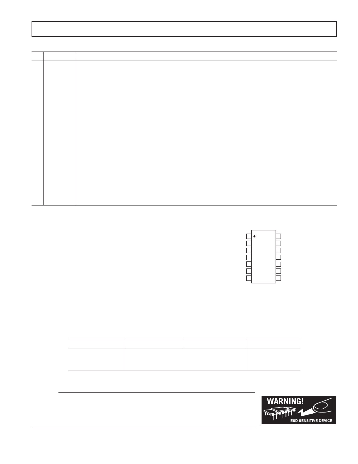
PIN CONFIGURATION
CAUTION
ESD (electrostatic discharge) sensitive device. Electrostatic charges as high as 4000 V readily
accumulate on the human body and test equipment and can discharge without detection. Although the
ADP3171 features proprietary ESD protection circuitry, permanent damage may occur on devices
–3–
subjected to high energy electrostatic discharges. Therefore, proper ESD precautions are recommended
to avoid performance degradation or loss of functionality.
REV. A
Page 4
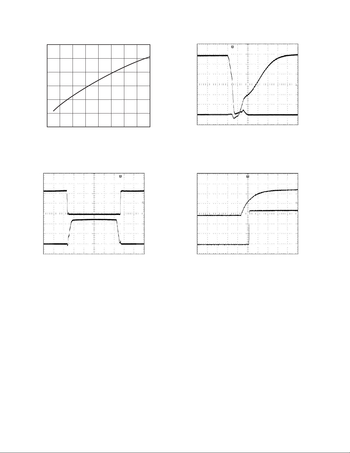
ADP3171–Typical Performance Characteristics
60
50
40
30
20
SUPPLY CURRENT – mA
10
2
0
0 200 400 600 800
OSCILLATOR FREQUENCY – kHz
TPC 1. Supply Current vs. Operating Frequency
Using MOSFETs of Figure 3
1
2
CH1 = 5.0V CH2 = 5.0V
M = 1.0sA: CH1 = 5.9V
TPC 2. Gate Switching Waveforms Using
MOSFETs of Figure 3
CH1 = 2.0V CH2 = 2.0V
M = 100ns A: CH1 = 5.88V
TPC 3. Driver Transition Waveforms Using
MOSFETs of Figure 3
1
2
CH1 = 5.0V CH2 = 500mV
M = 10.0ms A: CH1 = 5.9V
TPC 4. Power-On Start-Up Waveform
REV. A–4–
Page 5

Test Circuits
VCS–
ADP3171
GND
1
2
PWRGD
3
LRFB1
LRDRV1
4
FB
5
6
CS–
CS+
78
1.2V
DRVH
DRVL
VCC
LRFB2
LRDRV2
COMP
14
13
12
11
10
CT
AD820
9
+
1F 100nF
100
100nF
12V
V
LR1
10nF
ADP3171
ADP3171
GND
1
2
PWRGD
3
LRFB1
4
LRDRV1
5
FB
6
CS–
CS+
78
DRVH
DRVL
VCC
LRFB2
LRDRV2
COMP
14
13
+
12
11
10
9
CT
1F 100nF
V
LR2
10nF
VCC
Figure 1. Closed-Loop Output Voltage Accuracy Test Circuit
THEORY OF OPERATION
The ADP3171 uses a current-mode, constant off time control
technique to switch a pair of external N-channel MOSFETs in a
synchronous buck topology. Constant off time operation offers
several performance advantages, including the fact that no slope
compensation is required for stable operation. A unique feature
of the constant off time control technique is that since the off
time is fixed, the converter’s switching frequency is a function of
the ratio of input voltage to output voltage. The fixed off time is
programmed by the value of an external capacitor connected to
the CT pin. The on time varies in such a way that a regulated
output voltage is maintained as described below in the cycle-bycycle operation. Under fixed operating conditions, the on time
does not vary, and it varies only slightly as a function of load.
This means that switching frequency is fairly constant in most
applications.
Cycle-by-Cycle Operation
During normal operation (when the output voltage is regulated),
the voltage error amplifier and the current comparator are the
main control elements. During the on time of the high side
MOSFET, the current comparator monitors the voltage
between the CS+ and CS– pins. When the voltage level between
the two pins reaches the threshold level, the DRVH output is
switched to ground, which turns off the high side MOSFET.
The timing capacitor CT is then charged at a rate determined
by the off time controller. While the timing capacitor is charging,
the DRVL output goes high, turning on the low side MOSFET.
When the voltage level on the timing capacitor has charged to
the upper threshold voltage level, a comparator resets a latch.
The output of the latch forces the low side drive output to go
low and the high side drive output to go high. As a result, the
low side switch is turned off and the high side switch is turned on.
The sequence is then repeated. As the load current increases, the
output voltage starts to decrease. This causes an increase in the
output of the voltage error amplifier, which, in turn, leads to an
increase in the current comparator threshold, thus tracking the
load current. To prevent cross conduction of the external
MOSFETs, feedback is incorporated to sense the state of the driver
output pins. Before the low side drive output can go high, the
high side drive output must be low. Likewise, the high side drive
output is unable to go high while the low side drive output is high.
Output Crowbar
An added feature of using an N-channel MOSFET as the synchronous switch is the ability to crowbar the output with the
same MOSFET. If the output voltage is 20% greater than the
targeted value, the ADP3171 will turn on the lower MOSFET,
which will current-limit the source power supply or blow its
fuse, pull down the output voltage, and thus protect the load
from overvoltage destruction. The crowbar function releases at
approximately 50% of the nominal output voltage. For example,
if the output exceeds 1.44 V, the crowbar will turn on the lower
MOSFET. If the output is then pulled down to less than 0.6 V,
the crowbar will release, allowing the output voltage to recover
to 1.2 V if the fault condition has been removed.
On-Board Linear Regulator Controllers
The ADP3171 includes two linear regulator controllers to
provide a low cost solution for generating additional supply
rails. These regulators are internally set to 1.5 V (LR1) and 1.8 V
(LR2). The output voltage is sensed by the high input impedance LRFB(x) pin and compared to an internal fixed reference.
The LRDRV(x) pin controls the gate of
MOSFET, resulting in a negative feedback
additional components required are a capacitor and a resistor
for stability. Higher output voltages can be generated by placing
a resistor divider between the linear regulator output and its
respective LRFB pin. The maximum output load current is
determined by the size and thermal impedance of the external
power MOSFET that is placed in series with the supply and
controlled by the ADP3171.
The linear regulator controllers have been designed so that they
remain active even when the switching controller is in UVLO
mode to ensure that the output voltages of the linear regulators
will track the 3.3 V supply as required by Intel
cations. By diode OR-ing the VCC input of the IC to the 5 VSB
and 12 V supplies as shown in Figure 3, the switching output will
Figure 2. Linear Regulator Output Voltage
Accuracy Test Circuit
an external N-channel
loop. The only
®
design specifi-
REV. A
–5–
Page 6

ADP3171
5V
5VSB
12V
1F
C1
10F
D1
MBR052LT1
D2
MBR052LT1
5VSB
C2
Q1
2N7000
100pF
+
C5
1000F
C8
+
C6
4.7F
GND
1
2
PWRGD
3
LRFB1
4
LRDRV1
5
FB
6
CS–
CS+
78
R1
220
C3
1nF
R2
220
C4
R3
1k
R4
(249)
LRFB2
LRDRV2
DRVH
DRVL
VCC
COMP
CT
14
13
12
11
10
9
C9
150pF
C7
100nF
C10
100pF
22F
Q2
FDS6982
R8
10k
Q3
IRFU014
5VSB
L1
1.7H
8.25k
+
C13
220F
R9
C12
1F
R6
7.5m
820F 4
7.5m ESR (EACH)
C14 C15 C16 C17
1.5V, 5A
3.3VSB, 1.5A
Figure 3. Pentium® III Auxiliary Supply Generating 1.5 V, 1.5 V Standby, and 3.3 V Standby
be disabled in standby mode, but the linear regulators will
begin
conducting once VCC rises above about 1 V. During
startup, the
they reach their
linear outputs will track the 3.3 V supply up until
respective regulation points, regardless of the
state of the 12 V supply. Once the 12 V supply has exceeded
the 5 VSB supply, the controller IC will track the 12 V supply.
Once the 12 V supply has risen above the UVLO value, the
The timing capacitor can be calculated from the equation:
switching regulator will begin its start-up sequence.
APPLICATION INFORMATION
Specifications for a Design Example
The design parameters for a typical auxiliary supply for a Pentium III application (shown in Figure 3) are as follows:
Input Voltage: (V
Auxiliary Input: (V
Main Output: (V
LDO 1 Output: (1.5 VSB) = 1.5 V @ 35 mA
LDO 2 Output: (3.3 VSB) = 3.3 V @ 1.5 A
CT Selection for Operating Frequency
The ADP3171 uses a constant off time architecture, with t
determined by an external timing capacitor CT. Each time the
high side N-channel MOSFET switch turns on, the voltage across
) = 5 V
IN
) = 12 V
CC
) = 1.5 V @ 5 A
OUT
OFF
The nearest standard value is 150 pF. The converter operates at
the nominal operating frequency only at the above specified V
and at light load. At higher values of V
the operating frequency decreases due to the parasitic voltage
drops across the power devices. The actual
at V
where:
R
CT is reset to approximately 0 V. During the off time, CT is
charged by a constant current of 150 µA. Once CT reaches 3.0 V,
R
a new on time cycle is initiated. The value of the off time is
calculated using the continuous mode operating frequency.
Assuming a nominal operating frequency (f
) of 200 kHz at
NOM
R
an output voltage of 1.5 V, the corresponding off time is
R
1.5VSB, 35mA
t
=
OFF
t
=
OFF
tI
OFF CT
C
=
T
f
=×
MIN
t
OFF
f
=×
MIN
.
1
1
V
1
13555 15 75 315
µs
V
OUT
–
Vf
IN NOM
15
..V
–
5
V kHz
×
T(TH)
VI R R RV
IN O MAX DS ON HSF SENSE L OUT
VI R R RR
–( – )
IN O MAX DS ON HSF SENSE L DS ON LSF
VA m m m V
55 15 75
VA m m
1
×
=
–( )–
–( . )–.
–( .
1
×=
200
35 150
. µµsA
×++
() ()
×++
() () ()
×++
×+
35
sµ
×
3
V
ΩΩΩ
ΩΩ++=328
=
175
pF
mm
ΩΩ–)
, or under heavy load,
OUT
192
minimum frequency
= 1.5 V is calculated to be 192 kHz
OUT
DS(ON)HSF
is the resistance of the high side MOSFET
(see Equation 3),
(estimated value: 15 mΩ)
DS(ON)LSF
is the resistance of the low side MOSFET
(estimated value: 28 mΩ)
is the resistance of the sense resistor
SENSE
(estimated value: 7.5 mΩ)
is the resistance of the inductor (estimated value: 3 mΩ)
L
(1)
(2)
(3)
kHz
OUT
REV. A–6–
Page 7

ADP3171
Inductance Selection
The choice of inductance determines the ripple current in the
inductor. Less inductance leads to more ripple current, which
increases the output ripple voltage and the conduction losses in
the MOSFETs but allows using smaller size inductors and, for a
specified peak-to-peak transient deviation, output capacitors
with less total capacitance. Conversely, a higher inductance
means lower ripple current and reduced conduction losses, but
requires larger size inductors and more output capacitance for
the same peak-to-peak transient deviation. The following equation shows the relationship between the inductance, oscillator
frequency, peak-to-peak ripple current in an inductor, and input
and output voltages:
Vt
×
OUT OFF
L
=
I
L RIPPLE
()
(4)
For 2.5 A peak-to-peak ripple current, which corresponds to
approximately 50% of the 5 A full-load dc current in an inductor,
Equation 4 yields an inductance of
×
15 35
..
L =
Vs
25
.
=
21
A
.
Hµµ
A 1.7 µH inductor can be used, which gives a calculated ripple
current of 3 A at no load. The inductor should not saturate at
the peak current of 8 A and should be able to handle the sum of
the power dissipation caused by the average current of 5 A in
the winding and the core loss.
Designing an Inductor
Once the inductance is known, the next step is either to design
an inductor or find a standard inductor that comes as close as
possible to meeting the overall design goals. The first decision in
designing the inductor is to choose the core material. There are
several possibilities for providing low core loss at high frequencies. Two examples are the powder cores (e.g., Kool Mu
®
from
Magnetics, Inc.) and the gapped soft ferrite cores (e.g., 3F3 or
3F4 from Philips). Low frequency powdered iron cores should
be avoided due to their high core loss, especially when the
inductor value is relatively low and the ripple current is high.
Two main core types can be used in this application. Open
magnetic loop types such as beads, beads on leads, and rods and
slugs, provide lower cost but do not have a focused magnetic
field in the core. The radiated EMI from the distributed magnetic field may create problems with noise interference in the
circuitry surrounding the inductor. Closed-loop types such as
pot cores, PQ, U, and E cores, or toroids, cost more but have
much better EMI/RFI performance. A good compromise between
price and performance are cores with a toroidal shape.
There are many useful references for quickly designing a power
inductor. Table I gives some examples.
Table I. Magnetics Design References
Magnetic Designer Software
Intusoft (www.intusoft.com)
Designing Magnetic Components for High-Frequency DCDC Converters; by William T. McLyman, Kg Magnetics
ISBN 1-883107-00-08
Selecting a Standard Inductor
The companies listed in Table II can provide design consultation
and deliver power inductors optimized for high power applications
upon request.
Table II. Power Inductor Manufacturers
Coilcraft
(847) 639-6400
www.coilcraft.com
Coiltronics
(561) 752-5000
www.coiltronics.com
Sumida Electric Company
(510) 668-0660
www.sumida.com
Vishay-Dale
(203) 452-5664
www.vishay.com
R
SENSE
The value of R
is based on the required maximum output
SENSE
current. The current comparator of the ADP3171 has a minimum threshold of 69 mV. Note that this minimum value cannot
be used for the maximum specified nominal current, as headroom is needed for ripple current and transients.
The current comparator threshold sets the peak of the inductor
current yielding a maximum output current, I
O(MAX)
, which
equals the peak value less half of the peak-to-peak ripple current. Solving for R
allowing a 20% margin for overhead
SENSE
and using the minimum current sense threshold of 69 mV yields
R
SENSE
=
V
CS TH MIN
I
O MAX
()
()( )
I
RIPPLE
+
2
69
mV
=
5
A
=
.
10 6
3
A
+
2
mΩ
(5)
In this case, 7.5 m⍀ was chosen to provide ample headroom.
Once R
the point where current limit is reached, I
has been chosen, the maximum output current at
SENSE
OUT(CL)
, can be calcu-
lated using the maximum current sense threshold of 87 mV:
I
OUT CL
I
OUT CL
V
CS TH MAX
()( ) ( )
=
()
()
R
SENSE
87
mV
==
.
75
m
Ω
I
LRIPPLE
–
2
3
A
–.
10 1
2
A
(6)
At output voltages below 450 mV, the current sense threshold is
reduced to 54 mV, and the ripple current is negligible. Therefore,
the worst-case dead short output current is reduced to
I
OUT SC
()
V
R
CS SC
SENSE
()
54
.
75
mV
mAΩ
.===
72
(7)
To safely carry the current under maximum load conditions, the
sense resistor must have a power rating of at least:
PIR
ROSENSE
SENSE
2
=× = × =
2
575 188Am mW. Ω
(8)
REV. A
–7–
Page 8

ADP3171
Setting the Switcher Output Voltage
For this example, the resistor divider R3 and R4 set the output
voltage at 1.5 V by comparing the divided-down output to the
internal 1.2 V reference using
VV
=×+
OUT REF
C
Selection
OUT
The selection of C
R
4
1
R
3
is driven by the required effective series
OUT
(9)
resistance (ESR) and the desired output ripple. A good guide is
to limit the ripple voltage to 1% of the nominal output voltage.
It is assumed that the total ripple has two main contributors: 25%
from the C
ESR value. The correct value for C
C
OUT
bulk capacitance value and 75% from the C
OUT
It
OUT OFF
=
×∆∆025.
×
V
PP
can be determined by
OUT
OUT
(10)
and
V
×075. ∆
ESR
=
PP
I
∆
OUT
(11)
where
Vt
×
∆I
OUT
OUT OFF
=
L
OUT
(12)
and
∆VV
=×001.
PP OUT
(13)
Solving for this example:
Feedback Loop Compensation Design
Once the output capacitor C
chosen, the output circuit’s pole (f
and ESR values have been
OUT
) and zero (fZ) frequencies
P
can be calculated using
f
=
P
f
Z
×× +
2 π ()
=
××
2 π
1
CRESR
OUT OUT
1
C ESR
OUT
(14)
(15)
where:
V
R
OUT
OUT
=
I
OUT
(16)
For this example:
.
V
R
15
==
f
f
OUT
P
P
5
=
2 3280 0 3 3
πµ
××+
=
2 3280 3
πµ
××
.
Ω
03
A
1
Fm
(. )
ΩΩ
1
Fm
16 2
=
Ω
Hz
160
=
.
kHz
The compensation circuit is simply a capacitor (CC) connected
to the COMP pin. This makes the converter have a fast dynamic
response to load changes.
The switching frequency of the converter is 200 kHz. The crossover
frequency (fC) should be chosen at one-third the switching frequency,
or 70 kHz. The total gain of the compensation circuit (K) is
..
∆
∆
ESR
C
001 15 15
V
=× =
PP
..
15 35
I
=
OUT
.
075 15
=
335
=
OUT
.
025 15
VmV
Vs
17
×
3
As
µ
×
µ
H
.
mV
A
.
×
mV
×
3
=
.
375
=
µ
2800
=
A
m
Ω
µ
F
Four OSCON 820 µF/4 V capacitors would meet these require-
ments, giving a total capacitance of 3280 µF and an ESR of 3 mΩ.
Manufacturers such as Vishay, AVX, Elna, WIMA, and Sanyo
provide good high performance capacitors. Sanyo’s OSCON
capacitors have lower ESR for a given size at a somewhat higher
price. Choosing sufficient capacitors to meet the ESR requirement
for C
will normally exceed the amount needed to meet the
OUT
ripple current requirement.
g
K
=
where error amplifier transconductance (g
error amplifier gain (n
m
××× ×2 π
nCR f
iSC
) is 25, and the sense resistor (RS) is
i
) is 2.2 mmho, the
m
7.5 mΩ. The value of K is determined using the gain of the
power output circuit at f
, ESR, and K is
at f
C
G ESR
=
O
KG
×=
1
O
11
K
==
G ESR
O
As K is now known, the value of C
. The relationship between gain (GO)
C
can be determined by rear-
C
ranging Equation 17 as follows:
g ESR
×
C
=
C
C
=
C
m
nR f
×× ×
2
π
iSC
mmho
22 3
.
×× ×
22575 70
π
×
Ω
.mm kHz
Ω
=
80
pF
The closest standard value is 100 pF.
(17)
(18)
(19)
REV. A–8–
Page 9

ADP3171
Power MOSFETs
With this choice, the high-side MOSFET dissipation is
Two external N-channel power MOSFETs must be selected for
use with the ADP3171, one for the main switch and one for the
synchronous switch. The main selection parameters for the power
MOSFETs are the threshold voltage (V
(R
), and the gate charge (QG). Logic level
DS(ON)
), the ON resistance
GS(TH)
MOSFETs are
highly recommended. Only logic level MOSFETs with VGS ratings
higher than the absolute maximum value of VCC should be used.
The maximum output current I
requirement for the two power MOSFETs. When the ADP3171
is operating in continuous mode, the simplifying assumption
can be made that one of the two MOSFETs is always conducting the average load current. For V
the maximum duty ratio of the high-side FET is
determines the R
O(MAX)
= 5 V and V
IN
= 1.5 V,
OUT
DS(ON)
where the second term represents the turn-off loss of the MOSFET
and the third term represents the turn-on loss due to the stored
charge in the body diode of the low-side MOSFET. In the second term, QG is the gate charge to be removed from the gate for
turn-off and I
the value of QG for the FDS6982 is 12 nC and the peak gate
Dft
HSF MAX MIN OFF
()
D
HSF MAX
()
1
–
=+
()
=×
1 192 3 5 33kHz sµ
–.%
()
=
(20)
The maximum duty ratio of the low-side (synchronous rectifier)
MOSFET is
DD
LSF MAX HSF MAX() ()
–%==167
(21)
drive current provided by the ADP3171 is about 1 A. In the
third term, Q
low-side MOSFET at the valley of the inductor current. The
data sheet of the FDS6982 shows a value of 19 nC for this
parameter.
The low-side MOSFET dissipation is
The maximum rms current of the high-side MOSFET is
22
IIII
()()()()
ID
I
=×
() ()
HSF MAX HSF MAX
.
=×
033
()
HSF MAX
L VALLEY L VALLEY L PEAK L PEAK
22
.(. .).
+×+
375 375 625 625
AAAA
The maximum rms current of the low-side MOSFET is
()
+×+
3
3
.
=
29
(22)
A
Note that there are no switching losses in the low-side MOSFET.
CIN Selection and Input Current di/dt Reduction
In continuous inductor-current mode, the source current of the
high-side MOSFET is a square wave with a duty ratio of V
and an amplitude of one-half of the maximum output current.
ID
I
The R
=×
LSF MAX LSF MAX
() ()
.
=×
LSF MAX
067
()
for each MOSFET can be derived from the allowable
DS(ON)
22
IIII
L VALLEY L VALLEY L PEAK L PEAK
()()()()
22
.(..).
+×+
375 375 625 625
AAAA
())
+×+
()
3
3
=
.
41
(23)
A
prevent large voltage transients, a low ESR input capacitor
for the maximum rms current must be used. The maximum
capacitor current is given by
dissipation. If 10% of the maximum output power is allowed for
MOSFET dissipation, the total dissipation will be
For a ZA-type capacitor with 1000 µF capacitance and 6.3 V
PVI
D FETs OUT OUT MAX
() ( )
P
D FETs
()
Allocating half of the total dissipation for the high-side MOSFET
and half for the low-side MOSFET, and assuming that the resistive
loss of the high-side MOSFET is one-third and the switching
loss is two-thirds of its total, the required maximum MOSFET
.
=× ×
01
.. .
=× × =
01 15 65 975VA mW
(24)
voltage rating, the ESR is 24 mΩ and the maximum allowable
ripple current at 100 kHz is 2 A. At 105°C, at least two such
capacitors should be connected in parallel to handle the calculated ripple current. At 50°C ambient, however, a higher ripple
current can be tolerated, so one capacitor is adequate.
The ripple voltage across the input capacitor is
resistances will be
P
()
D FETs
R
()
DS ON HSF
R
()
DS ON LSF
=
×
3
I
()
HSF MAX
P
()
D FETs
=
×
2
I
()
LSF MAX
Note that there is a trade-off between converter efficiency and cost.
Larger MOSFETs reduce the conduction losses and allow higher
efficiency, but increase the system cost. A Fairchild FDB6982
dual MOSFET (high-side R
worst-case; and low-side R
DS(ON)
DS(ON)
worst-case) is a good choice in this application.
975
mW
=
22
×
329
975
=
22
×
241
.
mW
A
.
=
38
A
mΩ
mΩ
=
29
= 28 mΩ nominal, 35 mΩ
= 16 mΩ nominal, 22 mΩ
(25)
(26)
Linear Regulators
The linear regulators provide a low cost, convenient, and versatile
solution for generating moderate current supply rails. The maximum output load current is determined by the size and thermal
impedance of the external N-channel power MOSFET that is
placed in series with the supply and controlled by the ADP3171.
The output voltage is sensed at the LRFB × pin and compared
to an internal reference voltage in a negative feedback loop that
PR I
=×+
HSF DS ON HSF HSF MAX
VQ f
+× ×
P
HSF
+× × =
519 192 349
PR I
LSF DS ON LSF LSF MAX
P
LSF
IIDD
C rms O HSF HSF
I
C rms
VI
CRIPPLE O
VI
CRIPPLE O
() ( )
IN RR MIN
=×+
35 2 9
VnC kHz mW
=×
=×=
22 4 1 370mA mWΩ
=×
()
=× =
()
()
()
.
mA
Ω
is the gate turn-off current. From the data sheet,
G
is the charge stored in the body diode of the
RR
() ( )
.
503303324AA
=× +
=× +
.–. .
ESR
n
24
2
+××
.
5625 12 192
2
2
2
–
2
D
C
C
m
1
HSF MAX
nC f
××
CINMIN
Ω
××
11 192
VI Qf
×××
IN L PEAK G MIN
()
I
×
2
G
AnC kHz
×
21
A
2
033
.
=
26
mV
()
mF kHz
OUT
(27)
(28)
/
V
To
sized
rms
(29)
(30)
lN
REV. A
–9–
Page 10

ADP3171
keeps the output voltage in regulation. If the load is reduced or
increased, the MOSFET drive will also be reduced or increased
by the ADP3171 to provide a well regulated output voltage.
Output voltages higher than the fixed internal reference voltage
can be programmed by adding an external resistor divider. The
correct resistor values for setting the output voltage of the linear
regulators in the ADP3171 can be determined using
VV
OUT LR LRFB X
Assuming that R
=×
() ()
= 10 kΩ, V
L
Equation 31 to solve for R
k
V V
×−
10
Ω
()
R
=
U
10 3 3 18
=
R
U
OUT(LR) LRFB
V
LRFB
kVV
×−
ΩΩ..
()
V
18
.
UL
R
OUT(LR)
yields
U
2
L
= 3.3 V and rearranging
2
=
k
833
.
(31)
(32)
RR
+
The closest 1% resistor value is 8.25 kΩ.
Efficiency of the Linear Regulators
The efficiency and corresponding power dissipation of each of the
linear regulators are not determined by the ADP3171. Rather,
these are a function of input and output voltage and load current.
Efficiency is approximated by the formula
V
η= ×100%
V
OUT
IN
(33)
The corresponding power dissipation in the MOSFET, together
with any resistance added in series from input to output, is
given by
PVV I
=
()
LDO IN OUT OUT
×–
(34)
Minimum power dissipation and maximum efficiency are
accomplished by choosing the lowest available input voltage that
exceeds the desired output voltage. However, if the chosen input
source is itself generated by a linear regulator, its power dissipation will be increased in proportion to the additional current it
must now provide.
LAYOUT AND COMPONENT PLACEMENT GUIDELINES
The following guidelines are recommended for optimal performance
of a switching regulator in a PC system:
General Recommendations
1. For best results, a four-layer PCB is recommended. This
should allow the needed versatility for control circuitry
interconnections with optimal placement, a signal ground
plane, power planes for both power ground and the input
power (e.g., 5 V), and wide interconnection traces in the
rest of the power delivery current paths.
2. Whenever high currents must be routed between PCB
layers, vias should be used liberally to create several parallel current paths so that the resistance and inductance
introduced by these current paths is minimized and the via
current rating is not exceeded.
3. If critical signal lines (including the voltage and current
sense lines of the ADP3171) must cross through power
circuitry, it is best if a ground plane can be interposed
between those signal lines and the traces of the power
circuitry. This serves as a shield to minimize noise injection
into the signals at the expense of making signal ground a
bit noisier.
4. The GND pin of the ADP3171 should connect first to a
ceramic bypass capacitor (on the VCC pin) and then into
the analog ground plane. The analog ground plane should
be located below the ADP3171 and the surrounding
small signal components such as the timing capacitor
and compensation network. The analog ground plane
should connect to power ground plane at a single point; the
best location is the negative terminal of the last output
capacitor.
5. The output capacitors should also be connected as closely
as possible to the load (or connector) that receives the power
(e.g., a microprocessor core). If the load is distributed, the
capacitors should also be distributed, and generally in pro-
to where the load tends to be more dynamic. It is
portion
also advised to keep the planar interconnection path short
(i.e., have input and output capacitors close together).
6.
Absolutely avoid crossing any signal lines over the switching
power path loop, described below.
Power Circuitry
7. The switching power path should be routed on the PCB to
encompass the smallest possible area in order to minimize
radiated switching noise energy (i.e., EMI). Failure to take
proper precaution often results in EMI problems for the
entire PC system as well as noise-related operational problems
in the power converter control circuitry. The switching power
path is the loop formed by the current path through the
input capacitors, the two FETs, and the power
Schottky
diode, if used, including all interconnecting PCB traces and
planes. The use of short and wide interconnection traces is
especially critical in this path for two reasons: it minimizes
the inductance in the switching loop, which can cause high
energy ringing, and it accommodates the high current
demand with minimal voltage loss.
8.
A power Schottky diode (1 ~ 2 A dc rating) placed from the
lower MOSFET’s source (anode) to drain (cathode) will
help to minimize switching power dissipation in the upper
MOSFET. In the absence of an effective Schottky diode,
this dissipation occurs through the following sequence of
switching events. The lower MOSFET turns off in advance
of the upper MOSFET turning on (necessary to prevent
cross conduction). The circulating current in the power
converter, no longer finding a path for current through the
channel of the lower MOSFET, draws current through the
inherent body-drain diode of the MOSFET. The upper
MOSFET turns on, and the reverse recovery characteristic
of the lower MOSFET’s body-drain diode prevents the drain
voltage from being pulled high quickly. The upper MOSFET
then conducts very large current while it momentarily has
a high voltage forced across it, which translates into added
power dissipation in the upper MOSFET. The Schottky diode
minimizes this problem by carrying a majority of the circulating current when the lower MOSFET is turned off, and
by virtue of its essentially nonexistent reverse recovery time.
9. Whenever a power dissipating component (e.g., a power
MOSFET) is soldered to a PCB, the liberal use of vias, both
directly on the mounting pad and immediately surrounding
it, is recommended. Two important reasons for this are
REV. A–10–
Page 11

ADP3171
improved current rating through the vias (if it is a current
path), and improved thermal performance—especially if the
vias extended to the opposite side of the PCB where a plane
can more readily transfer the heat to the air.
10.
The output power path, though not as critical as the switching
power path, should also be routed to encompass a small area.
The output power path is formed by the current path through
the inductor, the current sensing resistor, the output
capacitors, and back to the input capacitors.
11.
For best EMI containment, the ground plane should extend
fully under all the power components. These are the input
capacitors, the power MOSFETs and Schottky diode,
the inductor, the current sense resistor, any snubbing
elements that might be added to dampen ringing, and the
output capacitors.
Signal Circuitry
12.
The output voltage is sensed and regulated between the GND
(which connects to the signal ground plane) and the
pin
FB–
pin. The output current is sensed (as a voltage) and
regulated
to avoid
signals, their
trace should be
CS+ and CS–
pair (CS+ should
13.
The CS+ and CS– traces should be Kelvin connected to the
current sense resistor so that the additional voltage drop due
to current flow on the PCB at the current sense resistor
connections does not affect the sensed voltage. It is desirable
to have the ADP3171 close to the output capacitor bank and
not in the output power path, so that any voltage drop
between the output capacitors and the GND pin is minimized,
and voltage regulation is not compromised.
between the CS– pin and the CS+ pin. In order
differential mode noise pickup in those sensed
loop areas should be small. Thus the FB–
routed atop the signal ground plane, and the
traces should be routed as a closely coupled
be over the signal ground plane as well).
REV. A
–11–
Page 12

ADP3171
OUTLINE DIMENSIONS
14-Lead Standard Small Outline Package [SOIC_N]
Narrow Body
(R-14)
Dimensions shown in millimeters and (inches)
0.3444 (8.75)
0.3367 (8.55)
0.1574 (4.00)
0.1497 (3.80)
14
1
8
0.2440 (6.20)
0.2284 (5.80)
7
C02711–0–3/05(A)
PIN 1
0.0098 (0.25)
0.0040 (0.10)
0.050 (1.27)
BSC
0.0688 (1.75)
0.0532 (1.35)
0.0192 (0.49)
0.0138 (0.35)
SEATING
PLANE
0.0099 (0.25)
0.0075 (0.19)
0.0196 (0.50)
0.0099 (0.25)
8ⴗ
0ⴗ
0.0500 (1.27)
0.0160 (0.41)
ⴛ 45ⴗ
Revision History
Location Page
3/05—Data Sheet Changed from REV. 0 to REV. A.
Changes to ORDERING GUIDE....................................................................................................................................................3
Updated OUTLINE DIMENSIONS.............................................................................................................................................12
–12–
REV. A
 Loading...