

Page 1

VRM 8.5 Compatible
a
FEATURES
Optimally Compensated Active Voltage Positioning
with Gain and Offset Adjustment (ADOPT™) for
Superior Load Transient Response
Complies with VRM 8.5 Specifications with Lowest
System Cost
5-Bit Digitally Programmable 1.05 V to 1.825 V Output
N-Channel Synchronous Buck Controller
Onboard 1.8 V Linear Regulator Controller
Total Accuracy 1% Over Temperature
High Efficiency Current-Mode Operation
Short Circuit Protection
Power Good Output
Overvoltage Protection Crowbar Protects
Microprocessors with No Additional External
Components
APPLICATIONS
Core and 1.8 V Standby Supplies for Next Generation
Intel Pentium® III Processors
Single Phase Core Controller
ADP3170
FUNCTIONAL BLOCK DIAGRAM
SD
GND
REF
LRFB
LRDRV
COMP
VCC
UVLO
AND BIAS
3.0V
REFERENCE
1.8V
ADP3170
REF
CT
OSCILLATOR
REF
SET
RESET
CROWBAR
CMP
VID
DAC
PWM
LOGIC
DAC +20%
DAC –20%
g
m
DRVH
DRVL
PGND
PWRGD
CS–
CS+
FB
GENERAL DESCRIPTION
The ADP3170 is a highly efficient output synchronous buck
switching regulator controller optimized for converting a 5 V
main supply into the core supply voltage required by next
generation Intel Celeron processors. The ADP3170 uses an
internal 5-bit DAC to read a voltage identification (VID)
code directly from the processor, which is used to set the
output voltage between 1.05 V and 1.825 V. The ADP3170
uses a current mode, constant off-time architecture to drive two
N-channel MOSFETs at a programmable switching frequency
that can be optimized for regulator size and efficiency.
The ADP3170 also uses a unique supplemental regulation technique called Analog Devices Optimal Positioning Technology
(ADOPT) to enhance load transient performance. Active
voltage positioning results in a dc/dc converter that meets the
stringent output voltage specifications for high performance
processors, with the minimum number of output capacitors and
smallest footprint. Unlike voltage-mode and standard current-
ADOPT is a trademark of Analog Devices, Inc.
Pentium is a registered trademark of Intel Corporation
VID25VID0VID1VID2VID3
mode architectures, active voltage positioning adjusts the output
voltage as a function of the load current so that it is always
optimally positioned for a system transient. The ADP3170 also
provides accurate and reliable short circuit protection and
adjustable current limiting. It also includes an integrated
overvoltage crowbar function to protect the microprocessor
from destruction in case the core supply exceeds the nominal
programmed voltage by more than 20%.
The ADP3170 contains a 1.8 V linear regulator controller that
is designed to drive an external N-channel MOSFET. This linear
regulator can be used to generate auxiliary voltages (such as 1.8 V
standby power) required in most motherboard designs, and has
been designed to provide a high bandwidth load-transient response.
The ADP3170 is specified over the commercial temperature range
of 0°C to 70°C and is available in a 20-lead TSSOP package.
REV. 0
Information furnished by Analog Devices is believed to be accurate and
reliable. However, no responsibility is assumed by Analog Devices for its
use, nor for any infringements of patents or other rights of third parties that
may result from its use. No license is granted by implication or otherwise
under any patent or patent rights of Analog Devices.
One Technology Way, P.O. Box 9106, Norwood, MA 02062-9106, U.S.A.
Tel: 781/329-4700 www.analog.com
Fax: 781/326-8703 © Analog Devices, Inc., 2001
Page 2

ADP3170–SPECIFICA TIONS
Parameter Symbol Conditions Min Typ Max Unit
FEEDBACK INPUT
Output Accuracy V
1.05 V Output Figure 1 1.039 1.05 1.061 V
1.5 V Output Figure 1 1.485 1.5 1.515 V
1.825 V Output Figure 1 1.807 1.825 1.843 V
Line Regulation ∆V
Input Bias Current I
Crowbar Trip Point V
Crowbar Reset Point % of Nominal DAC Voltage 40 50 60 %
Crowbar Response Time t
REFERENCE
Output Voltage V
Output Current I
VID INPUTS
Input Low Voltage V
Input High Voltage V
Input Current I
Pull-up Resistance R
Internal Pull-up Voltage 2.75 3.1 3.4 V
SHUTDOWN INPUT
Input Low Voltage V
Input High Voltage V
Input Current I
OSCILLATOR
Off Time T
CT Charge Current I
ERROR AMPLIFIER
Output Resistance R
Transconductance g
Output Current I
Maximum Output Voltage V
Output Disable Threshold V
–3 dB Bandwidth BW
CURRENT SENSE
Threshold Voltage V
Input Bias Current I
Response Time t
OUTPUT DRIVERS
Output Resistance R
Output Transition Time tR, t
LINEAR REGULATOR
Feedback Current I
LR Feedback Voltage V
Driver Output Voltage V
FB
OUT
FB
CROWBAR
CROWBAR
REF
REF
IL(VID)
IH(VID)
VID
VID
IL(SD)
IH(SD)
SD
CT
O(ERR)
m(ERR)
O(ERR)
COMP(MAX)
COMP(OFF)
ERR
CS(TH)
, I
CS+
CS–
CS
O(DRV[X])
F
LRFB
LRFB
LRDRV
(VCC = 12 V, I
= 150 A, TA = 0C to 70C, unless otherwise noted.)
REF
VCC = 10 V to 14 V 0.06 %
550nA
% of Nominal DAC Voltage 115 120 125 %
Overvoltage to DRVL Going High 400 ns
2.937 3.0 3.048 V
300 µA
0.8 V
2.3 V
VID(X) = 0 V 300 425 µA
16 kΩ
0.8 V
2.0 V
1 µA
= 25°C, CT = 200 pF 3.5 4.0 4.5 µs
A
T
= 25°C, V
A
T
= 25°C, V
A
in Regulation 130 150 170 µA
OUT
= 0 V 25 35 45 µA
OUT
1MΩ
2.05 2.2 2.35 mmho
FB = 0 625 µA
FB Forced to V
– 3% 3.0 V
OUT
600 750 900 mV
COMP = Open 500 kHz
FB Forced to V
– 3% 69 78 87 mV
OUT
FB ≤ 0.45 V 35 45 54 mV
0.8 V ≤ COMP ≤ 1 V 1 5 mV
CS+ = CS– = V
OUT
0.5 5 µA
CS+ – (CS–) > 87 mV 50 ns
to DRVH going low
I
= 50 mA 4.5 Ω
L
CL = 3000 pF 75 ns
0.3 1 µA
Figure 2, VCC = 4.5 V to 12.6 V 1.75 1.8 1.85 V
VCC = 4.5 V, V
= 0 V 4.2 V
LRFB(X)
1
–2–
REV. 0
Page 3
ADP3170
Parameter Symbol Conditions Min Typ Max Unit
POWER GOOD COMPARATOR
Undervoltage Threshold V
PWRGD(UV)
Undervoltage Hysteresis % of Nominal DAC Voltage 5 %
Overvoltage Threshold V
PWRGD(OV)
Overvoltage Reset Point % of Nominal DAC Voltage 40 50 60 %
Output Voltage Low V
OL(PWRGD)IPWRGD(SINK)
Response Time 200 ns
SUPPLY
DC Supply Current
UVLO Threshold Voltage V
2
I
CC
UVLO
UVLO Hysteresis 0.8 1 1.2 V
NOTES
1
All limits at temperature extremes are guaranteed via correlation using standard Statistical Quality Control (SQC).
2
Dynamic supply current is higher due to the gate charge being delivered to the external MOSFETs.
Specifications subject to change without notice.
ABSOLUTE MAXIMUM RATINGS*
VCC . . . . . . . . . . . . . . . . . . . . . . . . . . . . . . . –0.3 V to +15 V
DRVH, DRVL, LRDRV . . . . . . . . . . –0.3 V to VCC + 0.3 V
All Other Inputs & Outputs . . . . . . . . . . . . . . –0.3 V to +10 V
Operating Ambient Temperature Range . . . . . . . 0°C to 70°C
Operating Junction Temperature . . . . . . . . . . . . . . . . . 125°C
Storage Temperature Range . . . . . . . . . . . . –65°C to +150°C
. . . . . . . . . . . . . . . . . . . . . . . . . . . . . . . . . . . . . . 143°C/W
JA
Lead Temperature (Soldering, 10 sec) . . . . . . . . . . . . 300°C
Vapor Phase (60 sec) . . . . . . . . . . . . . . . . . . . . . . . . . . 215°C
Infrared (15 sec) . . . . . . . . . . . . . . . . . . . . . . . . . . . . . 220°C
*This is a stress rating only; operation beyond these limits can cause the device to
be permanently damaged. Unless otherwise specified, all voltages are referenced
to GND.
% of Nominal DAC Voltage 74 80 86 %
% of Nominal DAC Voltage 114 120 126 %
= 1 mA 250 500 mV
7.5 9.5 mA
6.75 7 7.25 V
ORDERING GUIDE
Model Temperature Range Package Description Package Option
ADP3170JRU 0°C to 70°C TSSOP RU-20
CAUTION
ESD (electrostatic discharge) sensitive device. Electrostatic charges as high as 4000 V readily
accumulate on the human body and test equipment and can discharge without detection. Although
the ADP3170 features proprietary ESD protection circuitry, permanent damage may occur on
devices subjected to high-energy electrostatic discharges. Therefore, proper ESD precautions are
recommended to avoid performance degradation or loss of functionality.
WARNING!
ESD SENSITIVE DEVICE
REV. 0
–3–
Page 4
ADP3170
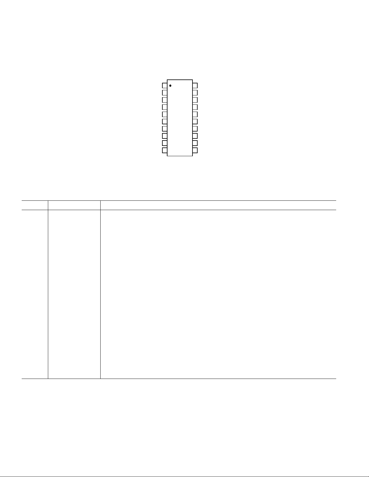
PIN CONFIGURATION
RU-20
VID3
VID2
VID1
VID0
VID25
PWRGD
REF
CS–
SD
FB
10
1
2
3
4
5
ADP3170
TOP VIEW
6
(Not to Scale)
7
8
9
20
19
18
17
16
15
14
13
12
11
GND
PGND
DRVH
DRVL
VCC
LRFB
LRDRV
COMP
CT
CS+
PIN FUNCTION DESCRIPTIONS
Pin No. Mnemonic Function
1–5 VID3, VID2, Voltage Identification DAC Inputs. These pins are pulled up to an internal reference,
VID1, VID0, providing a logic one if left open. The DAC output programs the FB regulation voltage from
VID25 1.05 V to 1.825 V.
6 PWRGD Open drain output that signals when the output voltage is in the proper operating range.
7 REF 3.0 V Reference Output.
8 SD Regulator Shutdown. Pulling this pin high turns off both MOSFETs of the switching
regulator. SD has no effect on the linear regulator controller.
9 FB Feedback Input. Error amplifier input for remote sensing of the output voltage.
10 CS– Current Sense Negative Node. Negative input for the current comparator.
11 CS+ Current Sense Positive Node. Positive input for the current comparator. The output current is
sensed as a voltage at this pin with respect to CS–.
12 CT External capacitor connected from CT to ground sets the OFF-Time of the device.
13 COMP Error Amplifier Output and Compensation Point. The voltage at this output programs the
output current control level between CS+ and CS–.
14 LRDRV Gate Drive for the 1.8 V linear regulator N-channel MOSFET.
15 LRFB Feedback Connections for the 1.8 V linear regulator controller.
16 VCC Supply Voltage for the ADP3170.
17 DRVL Low-Side MOSFET Drive. Gate drive for the synchronous rectifier N-channel MOSFET.
The voltage at DRVL swings from GND to VCC.
18 DRVH High-Side MOSFET Drive. Gate drive for the buck switch N-channel MOSFET. The voltage
at DRVH swings from GND to VCC.
19 PGND Power Ground. PGND should have a low impedance path to the source of the synchronous
MOSFET.
20 GND Small-Signal Ground. This ground reference can be used in conjunction with FB to provide
remote sensing of the output voltage at the CPU pins.
–4–
REV. 0
Page 5
5-BIT CODE
V
FB
1
2
3
4
5
6
7
8
9
10
ADP3170
VID3
VID2
VID1
VID0
VID25
PWRGD
REF
SD
FB
CS–
GND
PGND
DRVH
DRVL
VCC
LRFB
LRDRV
COMP
CS+
ADP3170
20
19
18
17
16
1F
15
14
13
12
CT
11
12V
100nF
100
100nF
AD820
1.2V
1
2
3
4
5
6
7
8
9
10
ADP3170
VID3
VID2
VID1
VID0
VID25
PWRGD
REF
SD
FB
CS–
GND
PGND
DRVH
DRVL
VCC
LRFB
LRDRV
COMP
CS+
20
19
18
17
16
15
14
13
12
CT
11
1F
10nF
100nF
VCC
V
LR
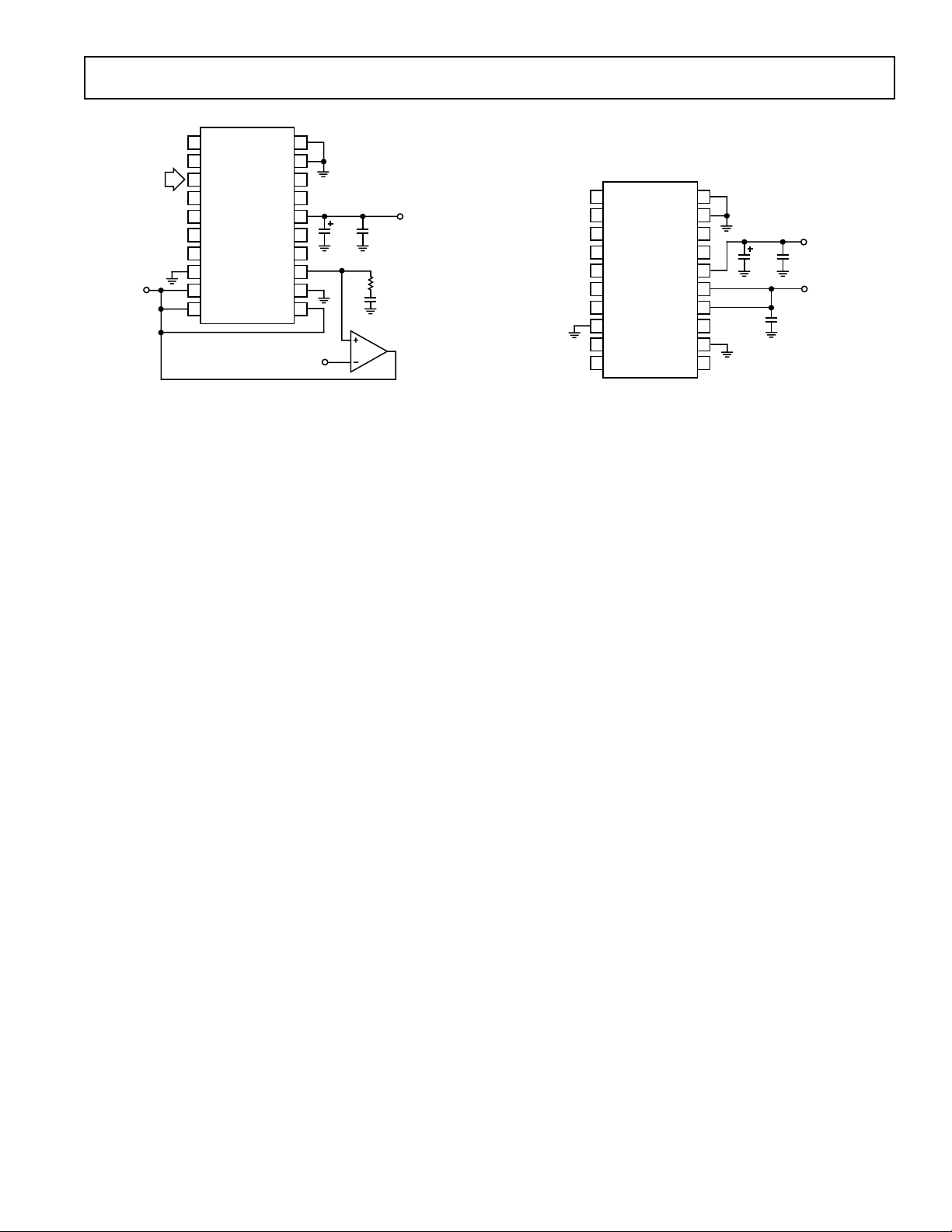
Figure 1. Closed-Loop Output Voltage Accuracy
Test Circuit
Figure 2. Linear Regulator Output Voltage Accuracy
Test Circuit
REV. 0
–5–
Page 6

ADP3170–Typical Performance Characteristics
100
SUPPLY CURRENT – mA
80
60
40
20
0
0
100
200 300 400 500
SWITHCHING FREQUENCY – kHz
TA = 25 C
TPC 1. Supply Current vs. Operating Frequency Using
MOSFETs of Figure 3
T
TEK RUN TRIG'D
VCC
1
V
CORE
2
CH1
5.00V CH2 500mV BW M 10.0ms A CH1
W
0.00000 s
TPC 4. Power-On Start-Up Waveform
25
20
15
TA = 25 C
= 1.5V
V
OUT
5.90VB
1
2
CH1 5.00V B
5.00V B
CH2 M 400ns A CH1 6.60V
W
W
TPC 2. Gate Switching Waveforms Using MOSFETs
of Figure 3
T
1
CH1 2.00V B
2.00V B
CH2 M 40.0ns A CH1 5.76V
W
W
TPC 3. Driver Transition Waveforms Using MOSFETs
of Figure 3
10
NUMBER OF PARTS – %
5
0
–0.6
OUTPUT ACCURACY – % OF NOMINAL
TPC 5. Output Accuracy Distribution
0.60
–6–
REV. 0
Page 7

ADP3170
THEORY OF OPERATION
The ADP3170 uses a current-mode, constant off-time control
technique to switch a pair of external N-channel MOSFETs in
a synchronous buck topology. Constant off-time operation
offers several performance advantages, including that no slope
compensation is required for stable operation. A unique feature
of the constant off-time control technique is that since the offtime is fixed, the converter’s switching frequency is a function
of the ratio of input voltage to output voltage. The fixed offtime is programmed by the value of an external capacitor
connected to the CT pin. The on-time varies in such a way
that a regulated output voltage is maintained as described
below in the cycle-by-cycle operation. Under fixed operating
conditions the on-time does not vary, and it varies only slightly
as a function of load. This means that switching frequency is
fairly constant in standard VRM applications.
Active Voltage Positioning
The output voltage is sensed at the CS– pin. A voltage error
amplifier, (g
), amplifies the difference between the output
m
voltage and a programmable reference voltage. The reference
voltage is programmed to between 1.05 V and 1.825 V by an
internal 5-bit DAC, which reads the code at the voltage identification (VID) pins. (Refer to Table I for output voltage vs. VID
pin code information.) A unique supplemental regulation technique called Analog Devices Optimal Positioning Technology
(ADOPT) adjusts the output voltage as a function of the load
current so that it is always optimally positioned for a load
transient. Standard (passive) voltage positioning, sometimes
recommended for use with other architectures, has poor dynamic
performance that renders it ineffective under the stringent
repetitive transient conditions specified in Intel VRM documents.
Consequently, such techniques do not allow the minimum
possible number of output capacitors to be used. ADOPT, as
used in the ADP3170, provides a bandwidth for transient
response that is limited only by parasitic output inductance.
This yields optimal load transient response with the minimum
number of output capacitors.
Reference Output
A 3.0 V reference is available on the ADP3170. This reference
is normally used to accurately set the voltage positioning using a
resistor divider to the COMP pin. In addition, the reference can
be used for other functions such as generating a regulated voltage with an external amplifier. The reference is bypassed with a
1 nF capacitor to ground. It is not intended to drive larger
capacitive loads, and it should not be used to provide more than
300 µA of output current.
Cycle-by-Cycle Operation
During normal operation (when the output voltage is regulated), the voltage error amplifier and the current comparator
are the main control elements. During the on-time of the high
side MOSFET, the current comparator monitors the voltage
between the CS+ and CS– pins. When the voltage level between
the two pins reaches the threshold level, the DRVH output is
switched to ground, which turns off the high side MOSFET.
The timing capacitor CT is then charged at a rate determined
by the off-time controller. While the timing capacitor is charging,
the DRVL output goes high, turning on the low side MOSFET.
When the voltage level on the timing capacitor has charged to
the upper threshold voltage level, a comparator resets a latch.
The output of the latch forces the low side drive output to go low
and the high side drive output to go high. As a result, the low side
switch is turned off and the high side switch is turned on. The
sequence is then repeated. As the load current increases, the output
voltage starts to decrease. This causes an increase in the output of
the voltage-error amplifier, which, in turn, leads to an increase in
the current comparator threshold, thus tracking the load current.
To prevent cross conduction of the external MOSFETs, feedback is incorporated to sense the state of the driver output pins.
Before the low side drive output can go high, the high side drive
output must be low. Likewise, the high side drive output is unable
to go high while the low side drive output is high.
Output Crowbar
An added feature of using an N-channel MOSFET as the synchronous switch is the ability to crowbar the output with the
same MOSFET. If the output voltage is 20% greater than the
targeted value, the ADP3170 will turn on the lower MOSFET,
which will current-limit the source power supply or blow its fuse,
pull down the output voltage, and thus save the microprocessor
from destruction. The crowbar function releases at approximately 50% of the nominal output voltage. For example, if the
output is programmed to 1.5 V, but is pulled up to 1.85 V or
above, the crowbar will turn on the lower MOSFET. If in this
case the output is pulled down to less than 0.75 V, the crowbar
will release, allowing the output voltage to recover to 1.5 V if
the fault condition has been removed.
Onboard Linear Regulator Controller
The ADP3170 includes a linear regulator controller to provide a
low cost solution for generating an additional supply rail. This
regulator is internally set to 1.8 V with ±2.8% accuracy. The
output voltage is sensed by the high input impedance LRFB
pin and compared to an internal fixed reference. The LRDRV
pin controls the gate of an external N-channel MOSFET
resulting in a negative feedback loop. The only additional
components required are a capacitor and resistor for stability.
Higher output voltages can be generated by placing a resistor
divider between the linear regulator output and its LRFB pin.
The maximum output load current is determined by the size
and thermal impedance of the external power MOSFET that
is placed in series with the supply and controlled by the ADP3170.
APPLICATION INFORMATION
Specifications for a Design Example
The design parameters for a typical VRM 8.5-compliant
Pentium III application (shown in Figure 3) are as follows:
Input voltage: (V
Auxiliary input: (V
VID setting voltage: (V
Nominal output voltage at no load (V
Nominal output voltage at maximum load (V
) = 5 V
IN
CC
) = 12 V
) = 1.8 V
OUT
) = 1.845 V
ONL
OFL
) = 1.771 V
Static output voltage drop based on a 3.2 mW load line
(R
) from no load to full load (V∆) = V
OUT
ONL
– V
OFL
=
1.845 V – 1.771 V = 74 mV
Maximum output current (I
O[MAX]
) = 23 A
REV. 0
–7–
Page 8

ADP3170
CT Selection for Operating Frequency
The ADP3170 uses a constant off-time architecture with t
OFF
determined by an external timing capacitor CT. Each time the
high-side N-channel MOSFET switch turns on, the voltage
across CT is reset to approximately 0 V. During the off-time,
CT is charged by a constant current of 150 µA. Once CT reaches
3.0 V, a new on-time cycle is initiated. The value of the off-time is
calculated using the continuous-mode operating frequency.
Assuming a nominal operating frequency (f
) of 200 kHz
NOM
at an output voltage of 1.8 V, the corresponding off-time is:
t
=
1
OFF
V
18
.
1
–
VkHz
5
V
OUT
–
Vf
IN NOM
×=
200
1
×=
1
32
. µ
s
(1)
The timing capacitor cab be calculated from the equation:
.3 2 150
tIVsA
×
OFF CT
C
=
T
TTH
()
µµ
=
×
3
V
≈
150
pF
(2)
The converter operates at the nominal operating frequency only
at the above-specified V
, or under heavy load, the operating frequency decreases
V
OUT
and at light load. At higher values of
OUT
due to the parasitic voltage drops across the power devices. The
actual minimum frequency at V
= 1.8 V is calculated to be
OUT
183 kHz (see Equation 3), where:
R
DS(ON)HSF
is the resistance of the high-side MOSFET
(estimated value: 6 mΩ)
R
DS(ON)LSF
is the resistance of the low-side MOSFET
(estimated value: 6 mΩ)
R
is the resistance of the sense resistor
SENSE
(estimated value: 2.5 mΩ)
R
is the resistance of the inductor
L
(estimated value: 3 mΩ)
Table I. Output Voltage vs. VID Code
VID3 VID2 VID1 VID0 VID25 V
OUT(NOM)
0 1 0 0 0 1.050 V
0 1 0 0 1 1.075 V
0 0 1 1 0 1.100 V
0 0 1 1 1 1.125 V
0 0 1 0 0 1.150 V
0 0 1 0 1 1.175 V
0 0 0 1 0 1.200 V
0 0 0 1 1 1.225 V
0 0 0 0 0 1.250 V
0 0 0 0 1 1.275 V
1 1 1 1 0 1.300 V
1 1 1 1 1 1.325 V
1 1 1 0 0 1.350 V
1 1 1 0 1 1.375 V
1 1 0 1 0 1.400 V
1 1 0 1 1 1.425 V
1 1 0 0 0 1.450 V
1 1 0 0 1 1.475 V
1 0 1 1 0 1.500 V
1 0 1 1 1 1.525 V
1 0 1 0 0 1.550 V
1 0 1 0 1 1.575 V
1 0 0 1 0 1.600 V
1 0 0 1 1 1.625 V
1 0 0 0 0 1.650 V
1 0 0 0 1 1.675 V
0 1 1 1 0 1.700 V
0 1 1 1 1 1.725 V
0 1 1 0 0 1.750 V
0 1 1 0 1 1.775 V
0 1 0 1 0 1.800 V
0 1 0 1 1 1.825 V
Inductance Selection
f
=×
MIN
1
s
33
.
µ
VI R R RV
––
1
t
OFF
×
VAm mmm
523 6 25 3 6
IN O MAX DS ON HSF SENSE L OUT
VI R R RR
––
IN O MAX DS ON HSF SENSE L DS ON LSF
( ) () ()
VAmm V
523 6 3 18
–( )–.
×+ +
–( . –
×++
() ()
×+
()
×++
()
ΩΩ
Ω ΩΩΩ))
The choice of inductance determines the ripple current in the
inductor. Less inductance leads to more ripple current, which
increases the output ripple voltage and the conduction losses in
the MOSFETs, but allows using smaller-size inductors and, for
a specified peak-to-peak transient deviation, output capacitors
with less total capacitance. Conversely, a higher inductance
means lower ripple current and reduced conduction losses, but
requires larger-size inductors and more output capacitance for
the same peak-to-peak transient deviation. The following equation shows the relationship between the inductance, oscillator
frequency, peak-to-peak ripple current in an inductor and input
and output voltages:
Vt
×
OUT OFF
L
=
I
L RIPPLE
()
(4)
–8–
=
(3)
=183 kHz
For 6 A peak-to-peak ripple current, which corresponds to
approximately 25% of the 23 A full-load dc current in an inductor,
Equation 4 yields an inductance of:
L
A
6
=
990
nH=
Vs
×
18 33
..µ
A 1 µH inductor can be used, which gives a calculated ripple
current of 5.9 A at no load. The inductor should not saturate at
the peak current of 26 A and should be able to handle the sum
of the power dissipation caused by the average current of 23 A
in the winding and the core loss.
REV. 0
Page 9

ADP3170
Designing an Inductor
Once the inductance is known, the next step is either to design
an inductor or find a standard inductor that comes as close as
possible to meeting the overall design goals. The first decision
in designing the inductor is to choose the core material. There
are several possibilities for providing low core loss at high frequencies. Two examples are the powder cores (e.g., Kool-M
®
from Magnetics, Inc.) and the gapped soft ferrite cores (e.g.,
3F3 or 3F4 from Philips). Low frequency powdered iron cores
should be avoided due to their high core loss, especially when
the inductor value is relatively low and the ripple current is high.
Two main core types can be used in this application. Open
magnetic loop types, such as beads, beads on leads, and rods
and slugs, provide lower cost but do not have a focused magnetic field in the core. The radiated EMI from the distributed
magnetic field may create problems with noise interference in
the circuitry surrounding the inductor. Closed-loop types,
L1
1.7H
5V
MBR052LT1
12V
5V SB
MBR052LT1
VTT PWRGD CLK
D1
D2
C1
1000FC21000FC31000FC41000FC51000F
C6
4.7nF
FROM
CPU
C7
100nF
C8
100pF
1
2
3
4
5
6
7
8
9
10
ADP3170
VID3
VID2
VID1
VID0
VID25
PWRGD
REF
SD
FB
CS–
R1
1k
U1
GND
PGND
DRVH
DRVL
VCC
LRFB
LRDRV
COMP
CT
CS+
20
19
18
17
16
15
14
13
12
11
C11
1nF
C19
150pF
C
OC
2.7nF
R4
220
R5
220
such as pot cores, PQ, U, and E cores, or toroids, cost more, but
have much better EMI/RFI performance. A good compromise
between price and performance are cores with a toroidal shape.
There are many useful references for quickly designing a power
inductor. Table II gives some examples.
Table II. Magnetics Design References
Magnetic Designer Software
Intusoft (http://www.intusoft.com)
Designing Magnetic Components for High-Frequency DC-DC
Converters
McLyman, Kg Magnetics
ISBN 1-883107-00-08
C12
22F
Q1
FDB7045L
L1
1H
Q2
FDB7045L
R
30.1k
1%
B
R6
2.5m
C13 C14 C15 C16 C17 C18 C19 C20
R
A
13.7k
1%
1000F 8
RUBYCON ZA SERIES
24m ESR (EACH)
C22
68pF
Q6
IRL3103
5V SB
10k
C21
1F
C23
220F
V
CC(CORE)
1.05V – 1.825V
23A
V
R7
1.8V SB
1.8V, 200mA
CORE
PWRGD
TO CPU
CC(CORE)
RTN
REV. 0
Figure 3. 24 A VRM 8.5-Compliant CPU Supply
–9–
Page 10

ADP3170
Selecting a Standard Inductor
The companies listed in Table III can provide design consultation and deliver power inductors optimized for high power
applications upon request.
Table III. Power Inductor Manufacturers
Coilcraft
(847) 639-6400
http://www.coilcraft.com
Coiltronics
(561) 752-5000
http://www.coiltronics.com
Sumida Electric Company
(408) 982-9660
http://www.sumida.com
R
SENSE
The value of R
is based on the required maximum output
SENSE
current. The current comparator of the ADP3170 has a minimum
threshold of 69 mV. Note that this minimum value cannot be
used for the maximum specified nominal current, as headroom
is needed for ripple current and transients.
The current comparator threshold sets the peak of the inductor
current yielding a maximum output current, I
O(MAX)
, which
equals the peak value less half of the peak-to-peak ripple current.
Solving for R
allowing a 20% margin for overhead and
SENSE
using the minimum current sense threshold of 69 mV yields:
R
SENSE
=
I
O MAX
V
CS TH MIN
()( )
+
()
I
RIPPLE
=
2
23
69
A
mV
+
.
59
2
A
266 Ω
=
.
m
(5)
In this case, 2.5 mΩ was chosen, assuming two 5 mΩ, 1 W
resistors in parallel (for power dissipation reasons). Once R
SENSE
has been chosen, the output current at the point where current
limit is reached, I
, can be calculated using the maximum
OUT(CL)
current sense threshold of 87 mV:
I
OUT CL
I
OUT CL
V
()( ) ( )
CS TH MAX
=
()
()
R
SENSE
mV
87
==
25
–
m
.
Ω
.
59
–
2
I
L RIPPLE
A
2
31 6
(6)
A
.
At output voltages below 450 mV, the current sense threshold is reduced to 54 mV, and the ripple current is negligible.
Therefore, the worst-case dead short output current is reduced to:
I
OUT SC
()
V
R
CS SC
()
SENSE
54
.
25
mV
m
A
.===
21 6
Ω
(7)
To safely carry the current under maximum load conditions, the
sense resistor must have a power rating of at least:
PIR Am W
R O SENSE
SENSE
2
=× = × =
2
23 25 133..Ω
(8)
Output Resistance
Intel’s VRM 8.5 specification requires that the regulator output
voltage measured at the CPU pins drops when the output current increases. The specified voltage drop corresponds to a dc
output resistance of:
VV
–.–.
R
OUT
ONL OFL
== =
I
∆
O
VV
1 845 1 771
A
23
.
32
m
Ω
(9)
The required dc output resistance can be achieved by terminating
amplifier with a resistor. The value of the total termina-
the g
m
tion resistance that will yield the correct dc output resistance is:
nR
×
I SENSE
R
=
T
gR
×
where n
amplifier to the PWM comparator and gm is the trans-
g
m
conductance of the g
m OUT
is the division ratio from the output voltage signal of the
I
m
25 2 5
=
mmho m
22 32
..
amplifier itself.
m
×
.
Ω
×
Ω
=
888
.
k
Ω
(10)
Output Offset
Intel’s VRM 8.5 specification requires that at no load the output
voltage of the regulator module be offset to a higher value than
the nominal voltage corresponding to the VID code. The offset
is introduced by realizing the total termination resistance of the
amplifier with a divider connected between the REF pin and
g
m
ground. The resistive divider introduces an offset to the output
of the g
of the g
amplifier that, when reflected back through the gain
m
stage, accurately positions the output voltage near its
m
allowed maximum at light load. Furthermore, the output of the
g
amplifier sets the current sense threshold voltage. At no load,
m
the current sense threshold is increased by the peak of the ripple
current in the inductor and reduced by the delay between sensing when the current threshold has been reached and when the
high side MOSFET actually turns off. These two factors are
combined with the inherent voltage (V
g
amplifier that commands a current sense threshold of 0 mV:
m
VV
=+
GNL ONL
VV
–
IN OUT
L
VV
=+
1
GNL
VV
–.
518
H
1
µ
IRn
tR n
×× ×
D SENSE I
..
59 32 25
60 2 5 25 1 224
×× ×=
L RIPPLE OUT I
()
Am
ns m V
××
2
××
Ω
2
..
Ω
The divider resistors (RA for the upper, and R
), at the output of the
GNL0
–
for the lower)
B
(11)
can now be calculated assuming that the internal resistance of
the g
m
R
R
amplifier (R
=
B
VV
REF GNL
R
=
B
VV
3 1 224
–.
888
.
–
T
) is 130 kΩ:
OGM
V
REF
k
Ω
gV
×+
–
m
V
3
mmho mV
22 45
–.
(12)
k
29 7
=
Ω
.
×
Choosing the nearest 1% resistor value gives RB = 30.1 kΩ.
Finally, R
is calculated:
A
–10–
REV. 0
Page 11

ADP3170
R
=
A
RR R
==
R
A
888
1
111
––
T OGM B
1
1
.
kM k
1
––
ΩΩ Ω
1
29 7
(13)
.
Ω
12 83
1
k
.
Choosing the nearest 1% resistor value gives RA = 12.7 kΩ.
C
Selection
OUT
The required equivalent series resistance (ESR) and capacitance
drive the selection of the type and quantity of the output capacitors. The ESR of the output filter capacitor bank must be equal
to or less than the specified output resistance of the voltage
regulator (3.2 mΩ). The capacitance must be large enough that
the voltage across the capacitor, which is the sum of the resistive
and capacitive voltage drops, does not move below or above the
initial resistive step while the inductor current ramps up or
down to the value corresponding to the new load current. One
can use, for example, eight ZA series capacitors from Rubycon,
which have a maximum ESR of 24 mΩ. These eight 1000 µF
capacitors would give an ESR of 3 mΩ.
As long as the capacitance of the output capacitor is above a
critical value, and the regulating loop is compensated with
Analog Devices’ proprietary compensation technique (ADOPT),
the actual value has no influence on the peak-to-peak deviation
of the output voltage to a full step change in the load current.
The critical capacitance can be calculated as follows:
C
OUT CRIT
C
OUT CRIT
=
()
=
()
O
(–)
×+
RVV
OUT OUT
23
.(.[–])
32 18 29
×+
Ω
mVmV
×
L
A
×=
1406
µ
HmF
(14)
.
I
The equivalent capacitance of the eight ZA series Rubycon
capacitors is 8 × 1 mF = 8 mF. In this case, the total capacitance
is safely above the critical value.
Feedback Loop Compensation Design for ADOPT
Optimized compensation of the ADP3170 allows the best possible containment of the peak-to-peak output voltage deviation.
The output current slew rate of any practical switching power
converter is inherently limited by the inductor to a value much
less than the slew rate of the load. Therefore, any sudden change
of load current will initially flow through the output capacitors,
and assuming that the capacitance of the output capacitor is
larger than the critical value defined by Equation 14, this will
produce a peak output voltage deviation equal to the ESR of the
output capacitor times the load current change.
The optimal implementation of voltage positioning, ADOPT,
will create an output impedance of the power converter that is
entirely resistive over the widest possible frequency range,
including dc, and equal to the specified dc output resistance.
With the wide-band resistive output impedance the output
voltage will droop in proportion with the load current at any
load current slew rate; this ensures the optimal positioning
and allows the minimization of the output capacitor.
With an ideal current-mode controlled converter, where the
inductor current would respond without delay to the command
signal, the resistive output impedance could be achieved by
having a single-pole roll-off of the voltage gain of the voltageerror amplifier. The pole frequency must coincide with the ESR
zero of the output capacitor.
The ADP3170 uses peak-current control, which is known to
have a nonideal, frequency-dependent command signal-toinductor current transfer function. The frequency dependence
manifests in the form of a pair of complex conjugate poles at
one-half of the switching frequency. A purely resistive output
impedance could be achieved by canceling the complex conjugate with zeros at the same complex frequencies and adding a
third pole equal to the ESR zero of the output capacitor. Such a
compensating network would be quite complicated. Fortunately, in practice, it is sufficient to cancel the pair of complex
conjugate poles with a single real zero placed at one-half of the
switching frequency.
Although the end result is not a perfectly resistive output impedance, the remaining frequency dependence causes only a slight
percentage of deviation from the ideal resistive response. The
single-pole and single-zero compensation can be easily implemented by terminating the g
combination of a resistor (R
value of the terminating resistor R
error amplifier with the parallel
m
) and a series RC network. The
T
was determined previously;
T
the capacitance and resistance of the series RC network are
calculated as follows:
C ESR
×
C
C
OUT
=
OC
mF m
83
=
OC
88827.
R
T
×Ω
k
Ω
(15)
nF
=
.
The closest standard value is 2.7 nF. The series resistance is:
R
=
Z
R
=
Z
2
π
Cf
××
OC MIN
2
2 7 188
π.
nF kHz
××
1255
=Ω
(16)
The nearest standard 5% resistor value is 1.2 kΩ. Note that this
resistor is only required when C
25% or less). In this example, C
approaches C
OUT
>> C
OUT
CRIT
, and RZ can
CRIT
(within
therefore be omitted.
REV. 0
–11–
Page 12

ADP3170
Power MOSFETs
Two external N-channel power MOSFETs must be selected for
use with the ADP3170, one for the main switch and one for the
synchronous switch. The main selection parameters for the power
MOSFETs are the threshold voltage (V
(R
), and the gate charge (QG). Logic-level MOSFETs are
DS(ON)
highly recommended. Only logic-level MOSFETs with V
higher than the absolute maximum value of V
The maximum output current I
O(MAX)
), the ON-resistance
GS(TH)
should be used.
CC
determines the R
ratings
GS
DS(ON)
requirement for the two power MOSFETs. When the ADP3170
is operating in continuous mode, the simplifying assumption can
be made that one of the two MOSFETs is always conducting
the average load current. For V
IN
= 5 V and V
= 1.8 V, the
OUT
maximum duty ratio of the high-side FET is:
Dft
HSF MAX MIN OFF
()
DkHzs
HSF MAX
()
1
–
=×
()
=×=
1183 33 40µ
–( . ) %
(17)
The maximum duty ratio of the low-side (synchronous rectifier)
MOSFET is:
DD
LSF MAX HSF MAX() ()
–%==160
(18)
The maximum rms current of the high-side MOSFET is:
ID
=×
HSF MAX HSF MAX
() ()
04
.
=×
I
HSF MAX
()
IIIvI
22
17 4 17 4 28 6 28 6
.(. .).
+×+
AAAA
22
+×
L VALLEY L VALLEY L PEAK L PEAK
( ) ( ) () ()
()
3
3
=
14 7
+
(19)
.
A
The maximum rms current of the low-side MOSFET is:
ID
=×
LSF MAX LSF MAX
() ()
.
06
HSF MAX
()
DS(ON)
=×
for each MOSFET can be derived from the
I
The R
22
IIII
....
17 4 17 4 28 6 28 6
AAAA
+×
L VALLEY L VALLEY L PEAK L PEAK
()()()()
22
+×
()
3
()
3
+
+
=
18
A
(20)
allowable dissipation. If 10% of the maximum output power is
allowed for MOSFET dissipation, the total dissipation will be:
.
=× ×
PVI
D FET OUT OUT MAX
() ( )
PVAW
D FET
()
01
s
.. .
=× × =
01 18 23 41
s
(21)
Allocating half of the total dissipation for the high-side MOSFET and
half for the low-side MOSFET, and assuming that the resistive loss of the high-side MOSFET is one-third, and the switching
loss is two-thirds of its portion, the required maximum MOSFET
resistances will be:
R
DS ON HSF
()
R
=
DS ON LS
()
P
D FETS
()
×
3
I
HSF MAX
P
D FETS
==×=
I
LSF MAX
2
()
()
22
()
41
=
×
3147
W
.
41
218
.
W
=
6
m
2
.
A
6 Ω
A
Ω
(22)
m
(23)
Note that there is a trade-off between converter efficiency and
cost. Larger MOSFETs reduce the conduction losses and allow
higher efficiency, but increase the system cost. A Fairchild
FDB7045L (R
= 4.5 mΩ nominal, 6 mΩ worst-case) is a
DS(ON)
good choice for both the low-side and high-side MOSFET.
With this choice, the high-side MOSFET dissipation is:
VI Qf
×××
2
IN L PEAK G MIN
A
×
21
()
I
×
2
G
+
(24)
+
PR I
=×+
HSF DS ON HSF HSF MAX
VQ f
IN RR MIN
Pm A
HSF
V nC kHz W
5 100 183 2 04
() ( )
××
×××
5 28 6 50 183
=× +
6147
Ω
2
.
×× =
.
.
A nC kHz
where the second term represents the turn-off loss of the
MOSFET and the third term represents the turn-on loss due to
the stored charge in the body diode of the low-side MOSFET.
In the second term, Q
the gate for turnoff and I
data sheet, the value of Q
is the gate charge to be removed from
G
is the gate turn-off current. From the
G
for the FDB7045L is 50 nC and the
G
peak gate drive current provided by the ADP3170 is about 1 A. In
the third term, Q
is the charge stored in the body diode of
RR
the low-side MOSFET at the valley of the inductor current.
The data sheet of the FDB7045L does not give that information, so an estimated value of 100 nC is used. The estimate is
based on information found on the data sheets of similar devices.
The low-side MOSFET dissipation is:
PR I
=×
LSF DS ON HSF HSF MAX
PmA W
LSF
() ( )
=×=
618194Ω
2
2
.
(25)
Note that there are no switching losses in the low-side MOSFET.
Surface mount MOSFETs are preferred in CPU core converter
applications due to their ability to be handled by automatic
assembly equipment. The TO-263 package offers the power
handling of a TO-220 in a surface mount package. However,
this package still needs adequate copper area on the PCB to
help move the heat away from the package.
The junction temperature for a given area of two-ounce copper
can be approximated using:
TPT
=×
()
AD AJJ
+θ
(26)
assuming:
= 45°C/W for 0.5 in
JA
= 36°C/W for 1 in
JA
= 28°C/W for 2 in
JA
2
2
2
For 1 in2 of copper area attached to each transistor and an
ambient temperature of 50°C:
TCWWCC
HSF
TCWWCC
LSFJJ
ooo
=×
=×
/.
28 2 06 50 108
()
ooo
/.
28 1 94 50 104
()
+=
+=
All of the above-calculated junction temperatures are safely
below the 175°C maximum specified junction temperature of
the selected MOSFETs.
–12–
REV. 0
Page 13

ADP3170
CIN Selection and Input Current di/dt Reduction
In continuous inductor-current mode, the source current of the
high-side MOSFET is a square wave with a duty ratio of V
V
and an amplitude of one-half of the maximum output
lN
OUT
/
current. To prevent large voltage transients, a low ESR input
capacitor sized for the maximum rms current must be used.
The maximum rms capacitor current is given by:
IIDD
IA A
=
C RMS O HSF HSF
()
=× =
C RMS
()
23 0 4 0 4 11 3
.–. .
2
–
2
(27)
For a ZA-type capacitor with 1000 µF capacitance and 6.3 V
voltage rating, the ESR is 24 mΩ and the maximum allowable
ripple current at 100 kHz is 2 A. At 105°C, at least six such
capacitors must be connected in parallel to handle the calcu-
lated ripple current. At 50°C ambient, however, a higher
ripple current can be tolerated, so five capacitors in parallel
are adequate.
The ripple voltage across the five paralleled capacitors is:
ESR
VI
C RIPPLE O
VA
C RIPPLE
=× +
()
=× ×
()
C
n
nC f
C
CINMIN
24
Ω
m
5045 1 183
D
HSF MAX
××
××
()
.
mF kHz
(28)
=23
120
mV
To further reduce the effect of the ripple voltage on the system
supply voltage bus and to reduce the input-current di/dt to
below the recommended maximum of 0.1 A/ms, an additional
small inductor (L > 1 µH @ 10 A) should be inserted between
the converter and the supply bus.
Linear Regulators
The linear regulator provides a low cost, convenient and versatile solution for generating a 1.8 V supply rail. The maximum
output load current is determined by the size and thermal
impedance of the external N-channel power MOSFET that is
placed in series with the supply and controlled by the ADP3170.
The output voltage is sensed at the LRFB pin and compared to
an internal reference voltage in a negative feedback loop which
keeps the output voltage in regulation. If the load is reduced or
increased, the MOSFET drive will also be reduced or increased
by the ADP3170 to provide a well regulated output voltage.
Output voltages higher than the fixed internal reference voltage
can be programmed by adding an external resistor divider.
Efficiency of the Linear Regulators
The efficiency and corresponding power dissipation of each
of the linear regulators are not determined by the ADP3170.
Rather, these are a function of input and output voltage and
load current. Efficiency is approximated by the formula:
V
η= ×100%
V
OUT
IN
(29)
The corresponding power dissipation in the MOSFET, together
with any resistance added in series from input to output is given by:
PVVI
=
()
LDO IN OUT OUT
×–
(30)
Minimum power dissipation and maximum efficiency are
accomplished by choosing the lowest available input voltage
that exceeds the desired output voltage. However, if the chosen
input source is itself generated by a linear regulator, its power
dissipation will be increased in proportion to the additional
current it must now provide.
3.3V
1F
ADP3170
LRDRV
LRFB
1.8V
V
1.8V, 2.2A
R
S
LR
250m
100F
10k
1k
68pF
Figure 4. Adding Overcurrent Protection to the Linear
Regulator
Implementing Current Limit for the Linear Regulators
The circuit of Figure 4 gives an example of a current limit protection circuit that can be used in conjunction with the linear
regulator. The output voltage is internally set by the LRFB pin.
The value of the current sense resistor may be calculated as
follows:
mV
540 540
R
≅==
S
I
O MAX
()
22
.
mV
A
250
m
Ω
(31)
The power rating of the current sense resistor must be at least:
PRI W
D R S O MAX
() ( )
S
2
.=× =
12
(32)
The maximum linear regulator MOSFET junction temperature with
a shorted output is:
TT VI
JJ
TCCWVAC
J
=+ × ×
MAX A C IN O MAX
() ()
=+ ××
MAX
()
θ
()
oo o
50 14 33 22 60
./ . .
()
=
(33)
which is within the maximum allowed by the MOSFET’s data
sheet specification. The maximum MOSFET junction temperature at nominal output is:
TCVVI
NOM C IN OUT O NOM
JJ
() ()
TCCWVVAC
NOM
J
()
o
=+×
50
=+ ×
50 14 33 18 2 54
θ
()
oo o
./ .–.
()
–
[]
×
×
[]
=
(34)
This example assumes an infinite heat sink. The practical limitation will be based on the actual heat sink used.
REV. 0
–13–
Page 14

ADP3170
LAYOUT AND COMPONENT PLACEMENT GUIDELINES
The following guidelines are recommended for optimal performance of a switching regulator in a PC system:
General Recommendations
1. For best results, a four-layer PCB is recommended. This
should allow the needed versatility for control circuitry
interconnections with optimal placement, a signal ground
plane, power planes for both power ground and the input
power (e.g., 5 V), and wide interconnection traces in the
rest of the power delivery current paths.
2. Whenever high currents must be routed between PCB
layers, vias should be used liberally to create several
parallel current paths so that the resistance and inductance introduced by these current paths is minimized and
the via current rating is not exceeded.
3. If critical signal lines (including the voltage and current
sense lines of the ADP3170) must cross through power circuitry, it is best if a ground plane can be interposed between
those signal lines and the traces of the power circuitry. This
serves as a shield to minimize noise injection into the signals
at the expense of making signal ground a bit noisier.
4. The GND pin of the ADP3170 should connect first to a
ceramic bypass capacitor (on the VCC pin) and then into the
analog ground plane. The analog ground plane should be
located below the ADP3170 and the surrounding smallsignal components, such as, the timing capacitor and
compensation network. The analog ground plane should
connect to power ground plane at a single point; the best
location being the negative terminal of the last output
capacitor.
5. The output capacitors should also be connected as closely as
possible to the load (or connector) that receives the power
(e.g., a microprocessor core). If the load is distributed,
the capacitors too should be distributed, and generally in
proportion to where the load tends to be more dynamic. It is
advised to keep the planar interconnection path short
(i.e., have input and output capacitors close together).
6. Absolutely avoid crossing any signal lines over the switching
power path loop, described below.
Power Circuitry
7. The switching power path should be routed on the PCB to
encompass the smallest possible area in order to minimize
radiated switching noise energy (i.e., EMI). Failure to take
proper precaution often results in EMI problems for the
entire PC system, as well as, noise-related operational
problems in the power converter control circuitry. The
switching power path is the loop formed by the current
path through the input capacitors, the two FETs and the
power Schottky diode, if used, including all interconnecting PCB traces and planes. The use of short and wide
interconnection traces is especially critical in this path for
two reasons: it minimizes the inductance in the switching
loop, which can cause high-energy ringing; and it accommodates the high current demand with minimal voltage loss.
8. A power Schottky diode (1 ~ 2 A dc rating) placed from
the lower MOSFET’s source (anode) to drain (cathode)
will help to minimize switching power dissipation in the
upper MOSFET. In the absence of an effective Schottky
diode, this dissipation occurs through the following sequence
of switching events. The lower MOSFET turns off in
advance of the upper MOSFET turning on (necessary to
prevent cross-conduction). The circulating current in the
power converter, no longer finding a path for current
through the channel of the lower MOSFET, draws current
through the inherent body-drain diode of the MOSFET.
The upper MOSFET turns on, and the reverse recovery
characteristic of the lower MOSFET’s body-drain diode
prevents the drain voltage from being pulled high quickly.
The upper MOSFET then conducts very large current
while it momentarily has a high voltage forced across it,
which translates into added power dissipation in the upper
MOSFET. The Schottky diode minimizes this problem
by carrying a majority of the circulating current when the
lower MOSFET is turned off, and by virtue of its essentially nonexistent reverse recovery time.
9. Whenever a power dissipating component (e.g., a power
MOSFET) is soldered to a PCB, the liberal use of vias,
both directly on the mounting pad and immediately surrounding it, is recommended. Two important reasons for
this are: improved current rating through the vias (if it is
a current path); and improved thermal performance—
especially if the vias extended to the opposite side of the PCB
where a plane can more readily transfer the heat to the air.
10. The output power path, though not as critical as the switching power path, should also be routed to encompass a small
area. The output power path is formed by the current path
through the inductor, the current sensing resistor, the output capacitors, and back to the input capacitors.
11. For best EMI containment, the ground plane should extend
fully under all the power components. These are: the input
capacitors, the power MOSFETs and Schottky diode, the
inductor, the current sense resistor, any snubbing elements
that might be added to dampen ringing and the output
capacitors.
Signal Circuitry
12. The output voltage is sensed and regulated between the
GND pin (which connects to the signal ground plane) and
the CS– pin. The output current is sensed (as a voltage)
and regulated between the CS– pin and the CS+ pin. In
order to avoid differential mode noise pickup in those
sensed signals, their loop areas should be small. Thus the
CS– trace should be routed atop the signal ground plane,
and the CS+ and CS– traces should be routed as a closely
coupled pair (CS+ should be over the signal ground plane
as well).
13. The CS+ and CS– traces should be Kelvin connected to
the current sense resistor so that the additional voltage drop
due to current flow on the PCB at the current sense resistor
connections does not affect the sensed voltage. It is desirable
to have the ADP3170 close to the output capacitor bank
and not in the output power path, so that any voltage drop
between the output capacitors and the GND pin is minimized, and voltage regulation is not compromised.
–14–
REV. 0
Page 15

OUTLINE DIMENSIONS
20 11
101
0.256 (6.50)
0.246 (6.25)
0.177 (4.50)
0.169 (4.30)
PIN 1
0.260 (6.60)
0.252 (6.40)
SEATING
PLANE
0.006 (0.15)
0.002 (0.05)
0.0118 (0.30)
0.0075 (0.19)
0.0256 (0.65)
BSC
0.0433 (1.10)
MAX
0.0079 (0.20)
0.0035 (0.090)
0.028 (0.70)
0.020 (0.50)
8
0
Dimensions shown in inches and (mm).
20-Lead TSSOP
(RU-20)
ADP3170
REV. 0
–15–
Page 16

C02620–1.5–7/01(0)
–16–
PRINTED IN U.S.A.
 Loading...