

Page 1
a
5-Bit Programmable Synchronous
Switching Regulator Controller
®
for Pentium
II Processor
ADP3152
FEATURES
5-Bit Digitally Programmable 1.8 V to 3.5 V Output
Voltage
Dual N-Channel Synchronous Driver
Total Output Accuracy 61% (08C to 708C)
High Efficiency
Current-Mode Operation
Short Circuit Protection
Power Good Output
Integrated Overvoltage Protection Crowbar
16-Lead SOIC Package
VRM 8.2 Compatible
APPLICATIONS
Desktop PC Power Supply for:
Pentium II Processor
Pentium Pro Processor
Pentium Processor
AMD–K6 Processor
VRM Modules
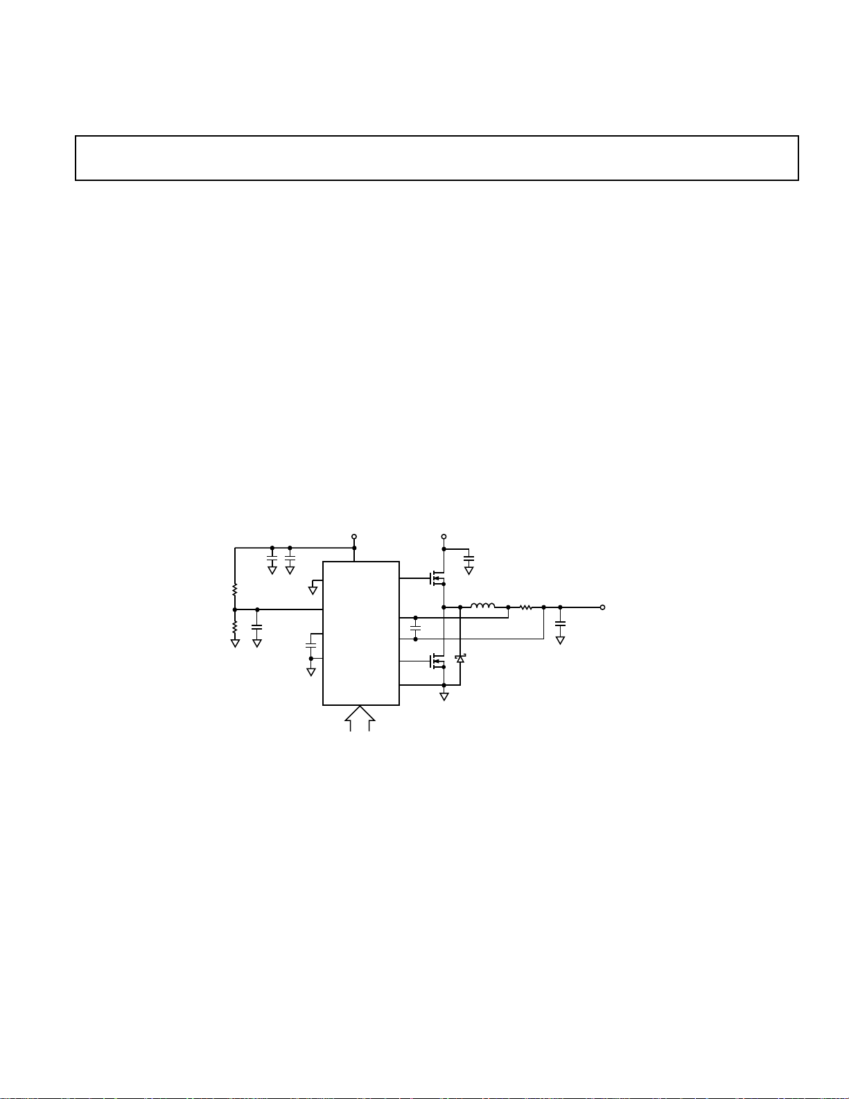
V
CC
+12V
C
COMP
150pF
1mF
SD
ADP3152
CMP
C
T
AGND
VID0–VID4
V
CC
DRIVE1
SENSE+
SENSE–
DRIVE2
PGND
22mF
R1
R2
IRL3103
1nF
IRL3103
GENERAL DESCRIPTION
The ADP3152 is a highly efficient synchronous switching regulator controller optimized for Pentium II Processor applications
where 5 V is stepped down to a digitally controlled output voltage between 1.8 V and 3.5 V. Using a 5-bit DAC to read a
voltage identification (VID) code directly from the processor,
the ADP3152 uses a current mode constant off-time architecture to generate its precise output voltage.
The ADP3152 drives two N-channel MOSFETS in a synchronous rectified buck converter, at a maximum switching frequency of 250 kHz. Using the recommended loop compensation
and guidelines, the ADP3152 provides a dc/dc converter that
meets Intel’s stringent transient specifications with a minimum
number of output capacitors and smallest footprint. Additionally,
the current mode architecture also provides guaranteed short
circuit protection and adjustable current limiting.
V
IN
+5V
+
C
IN
L
R
2.5mH
10BQ015
SENSE
6.7mV
V
O
1.8V–3.5V
+
14A
C
O
5-BIT CODE
Figure 1. Typical Application
Pentium is a registered trademark of Intel Corporation.
All other trademarks are the property of their respective holders.
REV. 0
Information furnished by Analog Devices is believed to be accurate and
reliable. However, no responsibility is assumed by Analog Devices for its
use, nor for any infringements of patents or other rights of third parties
which may result from its use. No license is granted by implication or
otherwise under any patent or patent rights of Analog Devices.
One Technology Way, P.O. Box 9106, Norwood, MA 02062-9106, U.S.A.
Tel: 781/329-4700 World Wide Web Site: http://www.analog.com
Fax: 781/326-8703 © Analog Devices, Inc., 1998
Page 2

ADP3152–SPECIFICATIONS
(08C ≤ TA ≤ +708C, V
= 12 V, VIN = 5 V, unless otherwise noted)
CC
Parameter Symbol Conditions Min Typ Max Units
OUTPUT ACCURACY
1.8 V Output Voltage V
O
With Respect to Nominal –1.0 1.0 %
2.8 V Output Voltage Output Voltage (Figure 13) –1.0 1.0 %
3.5 V Output Voltage –1.0 1.0 %
OUTPUT VOLTAGE LINE ∆V
O
I
= 10 A (Figure 2)
LOAD
REGULATION VIN = 4.75 V to 5.25 V 0.05 %
OUTPUT VOLTAGE LOAD ∆V
O
REGULATION 200 mA < I
INPUT DC SUPPLY CURRENT
Normal Mode I
1
Q
Shutdown T
(Figure 2)
< 14 A 0.1 %
LOAD
VSD = 0.8 V 3.7 4.5 mA
= +25°C, VID Pins Floating 140 250 µA
A
CURRENT SENSE THRESHOLD
VOLTAGE V8–V
VID PINS THRESHOLD V
, V1–V
16
7
V7 Forced to V
4
– 3% 125 145 165 mV
OUT
Low 0.6 V
High 2.0 V
VID PINS INPUT CURRENT I16, I1–I
VID0–VID4 PULL-UP RESISTANCE R
C
PIN DISCHARGE CURRENT I
T
OFFTIME t
DRIVER OUTPUT TRANSITION t
VID
9
OFF
, t
R
F
TIMES T
POSITIVE POWER GOOD TRIP POINT V
NEGATIVE POWER GOOD TRIP POINT V
POWER GOOD RESPONSE TIME t
CROWBAR TRIP POINT V
PWRGD
PWRGD
PWRGD
CROWBAR
VID
4
= 0 V 110 220 µA
20 30 kΩ
T
= +25°C
A
in Regulation 65 µA
V
OUT
V
= 0 V 2 10 µA
OUT
C
= 150 pF 1.8 2.45 3.2 µs
T
CL = 7000 pF (Pins 13, 14)
= +25°C 120 200 ns
A
Output Coming Into Regulation 5 8 %
Output Coming Into Regulation –8 –5 %
500 µs
% Above Output Voltage 9 15 24 %
ERROR AMPLIFIER
OUTPUT IMPEDANCE RO
ERR
145 kΩ
ERROR AMPLIFIER
TRANSCONDUCTANCE GM
ERR
2.2 mmho
ERROR AMPLIFIER MINIMUM
OUTPUT VOLTAGE V
CMPMIN
V7 Forced to V
+ 3% 0.8 V
OUT
ERROR AMPLIFIER MAXIMUM
OUTPUT VOLTAGE V
CMPMAXV7
ERROR AMPLIFIER BANDWIDTH –3 dB BW
ERR
Forced to V
– 3% 2.4 V
OUT
CMP = Open 500 kHz
SHUTDOWN (SD) PIN
Low Threshold SD
High Threshold SD
Input Current SD
NOTES
1
Dynamic supply current is higher due to the gate charge being delivered to the external MOSFETS.
All limits at temperature extremes are guaranteed via correlation using standard quality control methods.
Specifications are subject to change without notice.
L
H
IB
Part Active 0.6 V
Part in Shutdown 2.0 V
10 µA
–2– REV. 0
Page 3
ADP3152
WARNING!
ESD SENSITIVE DEVICE
PIN FUNCTION DESCRIPTIONS
Pin Mnemonic Function
1–4, 16 VID1–VID4, VD0 Voltage Identification DAC Input Pins. These pins are internally pulled up to V
logic one if left open. Leaving all five DAC inputs open results in placing the ADP3152 into
shutdown.
5 AGND Analog Ground Pin. This pin must be routed separately to the (–) terminal of C
6 SD Shutdown Pin. A logic high will place the ADP3152 in shutdown and disable the output. This
pin is internally pulled down.
7 SENSE– Connects to the internal resistor divider which, along with the VID code, sets the output volt-
age. Pin 7 is also the (–) input for the current comparator.
8 SENSE+ The (+) input for the current comparator. A threshold between Pins 8 and 7 set by the error
9C
T
amplifier in conjunction with R
External Capacitor CT from Pin 9 to ground sets the off time of the device.
, sets the current trip point.
SENSE
10 CMP Error Amplifier Compensation Point. The current comparator threshold increases with the Pin
10 voltage.
11 PWRGD Power Good Pin. An open drain signal to indicate that the output voltage is within a ±5% regu-
lation band.
12 V
CC
Input Voltage Pin.
13 DRIVE2 Gate Drive for the bottom synchronous N-channel MOSFET. The voltage at Pin 13 swings
from ground to V
CC
.
14 DRIVE1 Gate Drive for the top primary N-channel MOSFET. The voltage at Pin 14 swings from ground
to V
.
CC
15 PGND Driver Power Ground. Connects to the source of the bottom N-channel MOSFET and to the
(–) terminal of CIN.
providing a
REG
.
OUT
ABSOLUTE MAXIMUM RATINGS*
PIN CONFIGURATION
Input Supply Voltage (Pin 12) . . . . . . . . . . . . –0.3 V to +16 V
VID0–VID4, SD, PWRGD, CMP, CT . . . . . . . –0.3 V to V
DRIVE1, DRIVE2, SENSE+, SENSE– . . . . . . –0.3 V to V
Operating Temperature Range . . . . . . . . . . . . . 0°C to +70°C
Junction Temperature . . . . . . . . . . . . . . . . . . . . . . . . . . 150°C
␣ . . . . . . . . . . . . . . . . . . . . . . . . . . . . . . . . . . . . 110°C/W
θ
JA
Storage Temperature Range . . . . . . . . . . . . –65°C to +150°C
Lead Temperature Range (Soldering 10 sec) . . . . . . . .+300°C
*This is a stress rating only; operation beyond these limits can cause the device to
be permanently damaged.
CC
CC
VID1
VID2
VID3
VID4
AGND
SD
SENSE–
SENSE+
1
2
3
ADP3152
4
TOP VIEW
5
(Not to Scale)
6
7
8
ORDERING GUIDE
Temperature Package Package
Model Range Description Option
ADP3152AR 0°C to +70°C 16-Lead SOIC R-16A/SO-16
CAUTION
ESD (electrostatic discharge) sensitive device. Electrostatic charges as high as 4000 V readily
accumulate on the human body and test equipment and can discharge without detection.
Although the ADP3152 features proprietary ESD protection circuitry, permanent damage may
occur on devices subjected to high energy electrostatic discharges. Therefore, proper ESD
precautions are recommended to avoid performance degradation or loss of functionality.
16
15
14
13
12
11
10
9
VID0
PGND
DRIVE1
DRIVE2
V
CC
PWRGD
CMP
C
T
–3–REV. 0
Page 4
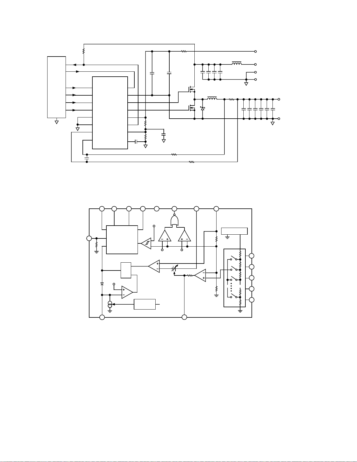
ADP3152
mP
SYSTEM
2nF
C
1mF
COMP
220V
22V
IRL3103
IRL3103
220V
3 32700mF/10V
++++
L1
2.5mH
10BQ015
1mF
R
SENSE
6.7mV
L2
1.7mH
V
+5V RTN
+12V RTN
2700mF 3 6 (10V)
+ + + + +
+
100kV VCC + 12V
+
22mF
ADP3152
1
2
3
4
5
6
7
8
VID1
VID2
VID3
VID4
AGND
SD
SENSE–
SENSE+
VID0
PGND
DRIVE1
DRIVE2
V
PWRGD
CMP
C
16
15
14
13
12
CC
11
10
9
T
C
T
150pF
R1
150kV
R2
39kV
1nF
Figure 2. Typical Application for Pentium II
SENSE–
8
7
ADP3152
REFERENCE
2R
1.20V
16
VID0
1
VID1
2
g
m
V
REF
R
VID2
3
VID3
SD
DRIVE1 DRIVE2 PGND
V
CC
12 14 13 15
NONOVERLAP
6
IN
V
T2
DRIVE
CROWBAR
S
Q
R
CMPT
V
REF
CMPI
AGND
+ 15%
V
REF
PWRGD
+ 5% V
V
T1
SENSE+
115
DELAY
– 5%
REF
IN
+ 5V
V
O
1.8V–3.5V
0-14A
RTN
4
OFF-TIME
CONTROL
9
C
T
SENSE–
10
CMP
DAC
VID4
Figure 3. Functional Block Diagram
–4– REV. 0
Page 5

OPERATING FREQUENCY – kHz
45 397
58 83 134
GATE CHARGE CURRENT – mA
45
40
0
20
15
10
5
35
25
30
Qn + Qn = 100nC
10ms/DIV
OUTPUT CURRENT
14A TO 1A
OUTPUT VOLTAGE
20mV/DIV
OUTPUT ACCURACY – %
NUMBER OF PARTS
15
0
–0.55
–0.5
–0.45
25
20
10
5
–0.4
–0.35
–0.3
–0.25
–0.2
–0.15
–0.1
–0.05
0
0.05
0.1
0.15
0.2
0.25
0.3
0.35
0.4
0.45
0.5
TA = +258C
SEE FIGURE 13
Typical Performance Characteristics–ADP3152
100
95
90
85
V
= +2.0V
OUT
80
EFFICIENCY – %
75
70
65
4.2 5.6 7.0 9.8 11.2 12.68.4
1.4 2.8 14.0
OUTPUT CURRENT – Amps
V
OUT
V
SEE FIGURE 2
= +3.5V
= +2.8V
OUT
Figure 4. Efficiency vs. Output Current
V
= +3.5V, I
OUT
PRIMARY
N-DRIVE
1
2
DRIVER OUTPUT
SECONDARY
N-DRIVE
DRIVER OUTPUT
SEE FIGURE 2
= 10A
OUT
450
400
350
300
250
200
150
FREQUENCY – kHz
100
50
0
50 100 800
200 300 400 500 600 700
TIMING CAPACITOR – pF
Figure 5. Frequency vs. Timing
Capacitor
SEE FIGURE 2
2
Figure 6. Gate Charge Supply Current vs. Operating Frequency
DRIVE 1 AND 2 = 5V/DIV
Figure 7. Gate Switching Waveforms
OUTPUT VOLTAGE
20mV/DIV
OUTPUT CURRENT
1A TO 14A
Figure 10. Transient Response,
1A–14 A of Figure 2 Circuit
500ns/DIV
Figure 8. Driver Transition Waveforms
100ns/DIV
Figure 9. Transient Response, 14 A–1A
of Figure 2 Circuit
VCC VOLTAGE
5V/DIV
3
REGULATOR
OUTPUT VOLTAGE
1V/DIV
4
10ms
Figure 11. Power-On Start-Up
Waveforms
–5–REV. 0
Figure 12. Output Accuracy
Distribution, V
OUT
= 2.8 V
Page 6

ADP3152
12V
V
DRIVE1
DRIVE2
SENSE+
SENSE–
PGND
CC
+
1mF
0.1mF
V
OUT
5-BIT
4700pF
1.2V
CODE
1kV
100kV
␣
VID0–
VID4
SD
CMP
C
T
ADP3152
AGND
OP27
0.1mF
Figure 13. Closed-Loop Test Circuit for Accuracy
APPLICATION INFORMATION
The ADP3152 uses a current-mode, constant-off-time control
technique to switch a pair of external N-channel MOSFETs in
a synchronous rectified buck converter application. Due to the
constant-off-time operation, no slope compensation is needed.
A unique feature of the constant-off-time control technique is
that the converter’s frequency becomes a function of the ratio of
input voltage to output voltage. The off time is determined by
the value of the external capacitor connected to the C
pin.
T
The on time varies in such a way that a regulated output voltage is maintained.
The output voltage is sensed by an internal voltage divider that
is connected to the Sense– pin. A voltage-error amplifier g
m
compares the values of the divided output voltage with a reference voltage. The reference voltage is set by an onboard 5-bit
DAC, which reads the code present at the voltage identification
(VID) pins and converts it to a precise value between 600 mV
and 1.167 V. Refer to Table I for the output voltage vs. VID pin
code information.
During continuous-inductor-current mode of operation, the
voltage-error amplifier g
and the current comparator CMPI
m
are the main control elements. During the on time of the high
side MOSFET, the current comparator CMPI monitors the
voltage between the Sense+ and Sense– pins. When the voltage
level between the two pins reaches the threshold level V
T1
, the
high side drive output is switched to zero, which turns off the
high side MOSFET. The timing capacitor C
is now discharged
T
at a rate determined by the off time controller. In order to
maintain a ripple current in the inductor, which is independent
of the output voltage, the discharge current is made proportional to the value of the output voltage (measured at the
Sense– pin). While the timing capacitor is discharging, the low
side drive output goes high, turning on the low side MOSFET.
When the voltage level on the timing capacitor has discharged
to the threshold voltage level V
, comparator CMPT resets
T2
the SR flip-flop. The output of the flip-flop forces the low side
drive output to go low and the high side drive output to go high.
As a result, the low side switch is turned off and the high side
switch is turned on. The sequence is then repeated. As the load
current increases, the output voltage starts to decrease. This
causes an increase in the output of the voltage-error amplifier,
which, in turn, leads to an increase in the current comparator
threshold V
thus tracking the load current.
T1,
Table I. Output Voltage vs. VID Code
VID4 VID3 VID2 VID1 VID0 VOUT
0 1 1 1 1 1.80
0 1 1 1 0 1.80
0 1 1 0 1 1.80
0 1 1 0 0 1.80
0 1 0 1 1 1.80
0 1 0 1 0 1.80
0 1 0 0 1 1.80
0 1 0 0 0 1.80
0 0 1 1 1 1.80
0 0 1 1 0 1.80
0 0 1 0 1 1.80
0 0 1 0 0 1.85
0 0 0 1 1 1.90
0 0 0 1 0 1.95
0 0 0 0 1 2.00
0 0 0 0 0 2.05
1 1 1 1 1 Shutdown
1 1 1 1 0 2.10
1 1 1 0 1 2.20
1 1 1 0 0 2.30
1 1 0 1 1 2.40
1 1 0 1 0 2.50
1 1 0 0 1 2.60
1 1 0 0 0 2.70
1 0 1 1 1 2.80
1 0 1 1 0 2.90
1 0 1 0 1 3.00
1 0 1 0 0 3.10
1 0 0 1 1 3.20
1 0 0 1 0 3.30
1 0 0 0 1 3.40
1 0 0 0 0 3.50
To prevent cross conduction of the external MOSFETs, feedback is incorporated to sense the state of the driver output pins.
Before the low side drive output can go high, the high side drive
output must be low. Likewise, the high side drive output is
unable to go high while the low side drive output is high.
Power Good
The ADP3152 has an internal monitor which monitors the
output voltage and drives the PWRGD pin of the device. This
pin is an open drain output whose high level (when connected
to a pull-up resistor) indicates that the output voltage has been
within a ±5% regulation band of the targeted value for more
than 500 µs. The PWRGD pin will go low if the output is outside the regulation band for more than 500 µs.
Output Crowbar
An added feature of using an N-channel MOSFET as the synchronous switch is the ability to crowbar the output with the
same MOSFET. If the output voltage is 15% greater than the
desired regulated value, the ADP3152 will turn on the lower
MOSFET, which will current-limit the source power supply or
blow its fuse, pull down the output voltage, and thus save the
–6– REV. 0
Page 7

ADP3152
expensive microprocessor from destruction. The crowbar function releases at approximately 50% of the nominal output voltage. For example, if the output is programmed to 2.0 V, but is
pulled up to 2.3 V or above, the crowbar will turn on the lower
MOSFET. If in this case the output is pulled down to less than
1.0 V, the crowbar will release, allowing the output voltage to
recover to 2.0 V.
Shutdown
The ADP3152 has a shutdown pin which is pulled logic low by
an internal resistor. In this condition the device functions normally. This pin should be pulled high externally to disable the
output drives.
Calculation of Component Values
The design parameters for a typical 300 MHz Pentium II application (Figure 2) are as follows:
Input voltage: V
Auxiliary input: V
Output voltage: V
= 5 V
IN
CC
= 2.8 V
O
= 12 V
Maximum output current:
= 14.2 Adc
I
OMAX
Minimum output current:
= 0.8 Adc
I
OMIN
Static tolerance of the supply voltage for the processor core:
= 100 mV
∆V
OST+
= –60 mV
∆V
OST–
Transient tolerance (for less than 2 µs) of the supply voltage for
the processor core when the load changes between the minimum
and maximum values with a di/dt of 30 A/µs:
= 130 mV
∆V
OTR+
= –130 mV
∆V
OTR–
Input current di/dt when the load changes between the minimum and maximum values: less than 0.1 A/µs
The above requirements correspond to Intel’s published power
supply requirements based on VRM 8.2 guidelines.
CT Selection for Operating Frequency
The ADP3152 uses a constant-off-time architecture with t
OFF
determined by an external timing capacitor CT. Each time the
high side N-channel MOSFET switch turns on, the voltage
across C
C
T
is reset to approximately 3.3 V. During the off time,
T
is discharged by a constant current of 65 µA to 2.3 V, that is
by 1 V. The value of the off time is calculated from the preferred continuous-mode operating frequency. Assuming a nominal operating frequency of f
= 2.8 V, the corresponding off time is:
of V
O
= 200 kHz at an output voltage
NOM
The timing capacitor can be calculated from the equation:
×65 µA
t
OFF
C
=
T
1V
=143 pF
The converter operates at the nominal operating frequency only
at the above specified V
and at light load. At higher VO, and
O
heavy load, the operating frequency decreases due to the parasitic voltage drops across the power devices. The actual minimum frequency at V
= 2.8 V is calculated to be 160 kHz (see
O
Equation 1 below). Where
I
IN
R
IN
is the input dc current (assuming an efficiency
of 90%, I
= 9 A)
IN
is the resistance of the input filter (estimated
value: 7 mΩ)
R
DS(ON)HSF
is the resistance of the high side MOSFET
(estimated value: 10 mΩ)
R
DS(ON)LSF
is the resistance of the low side MOSFET
(estimated value: 10 mΩ)
R
SENSE
is the resistance of the sense resistor
(estimated value: 7 mΩ)
R
L
is the resistance of the inductor (estimated
value: 6 mΩ)
CO Selection—Determining the ESR
The selection of the output capacitor is driven by the required
ESR and capacitance C
. The ESR must be small enough that
O
both the resistive voltage deviation due to a step change in the
load current and the output ripple voltage stay below the values
defined in the specification of the supplied microprocessor. The
capacitance, C
, must be large enough that the output is held
O
up while the inductor current ramps up or down to the value
corresponding to the new load current.
The total static tolerance of the Pentium II processor is 160 mV.
Taking into account the ±1% setpoint accuracy of the ADP3152,
and assuming a 0.5% (or 14 mV) peak-to-peak ripple, the allowed static voltage deviation of the output voltage when the
load changes between the minimum and maximum values is
0.08 V. Assuming a step change of ∆I = I
OMAX–IOMIN
= 13.4 A,
and allocating all of the total allowed static deviation to the
contribution of the ESR sets the following limit:
R
=ESR
E MAX
()
MAX1
=
0.08
13.4
= 5. 9 m Ω
t
= 1–
OFF
MIN
1
=
t
OFF
f
V
×
VIN– IINRIN– I
V
O
V
IN
– IINRIN– I
IN
1
=2.2 µs
f
NOM
OMAX(RDS(ON)HSF+RSENSE+RL
OMAX(RDS(ON)HSF+RSENSE+RL
– R
)–V
O
DS(ON)LSF
=160 kHz
)
(1)
–7–REV. 0
Page 8

ADP3152
The output filter capacitor must have an ESR of less than
5.9 mΩ. One can use, for example, six FA type capacitors from
Panasonic, with 2700 µF capacitance, 10 V voltage rating, and
34 mΩ ESR. The six capacitors have a total typical ESR of
~ 5 mΩ when connected in parallel.
Inductor Selection
The minimum inductor value can be calculated from ESR, off
time, dc output voltage and allowed peak-to-peak ripple voltage.
L
MIN1
V
OtOFFRE( MAX )
=
V
RIPPLE , p −p
2.8 ×2. 2 µ×5.9 m
=
14 m
= 2.6 µH
The minimum inductance gives a peak-to-peak ripple current of
2.15 A, or 15% of the maximum dc output current I
OMAX
.
The inductor peak current in normal operation is:
I
LPEAK
= I
OMAX
+ I
/2 = 15.3 A
RPP
The inductor valley current is:
I
LVALLEY
= I
LPEAK
– I
RPP
= 13 A
The inductor for this application should have an inductance
of 2.6 µH at full load current and should not saturate at the
worst-case overload or short circuit current at the maximum
specified ambient temperature. A suitable inductor is the
CTX12-13855 from Coiltronics, which is 4.4 µH at 1 A and
about 2.5 µH at 14.2 A.
Tips for Selecting Inductor Core
Ferrite designs have very low core loss, so the design should
focus on copper loss and on preventing saturation. Molypermalloy,
or MPP, is a low loss core material for toroids, and it yields the
smallest size inductor, but MPP cores are more expensive than
ferrite cores or the Kool Mµ
®
cores from Magnetics, Inc. The
lowest cost core is made of powdered iron, for example the #52
material from Micrometals, Inc., but yields the largest size
inductor.
CO Selection—Determining the Capacitance
The minimum capacitance of the output capacitor is determined
from the requirement that the output be held up while the inductor current ramps up (or down) to the new value. The minimum capacitance should produce an initial dv/dt which is equal
(but opposite in sign) to the dv/dt obtained by multiplying the
di/dt in the inductor and the ESR of the capacitor.
– I
I
C
MIN
OMAX
=
RE(di /dt )
OMIN
14.2–0.8
=
5.9 m (2.2 / 4.4 µH)
= 4.5 mF
In the above equation the value of di/dt is calculated as the
smaller voltage across the inductor (i.e., V
rather than VO)
IN–VO
divided by the maximum inductance (4.4 µH) of the CTX12-
13855 inductor from Coiltronics. The parallel-connected six
2700 µF/10 V FA series capacitors from Panasonic have a total
capacitance of 16,200 µF, so the minimum capacitance require-
ment is met with ample margin.
R
SENSE
The value of R
is based on the required output current.
SENSE
The current comparator of the ADP3152 has a threshold range
that extends from 0 mV to 125 mV (minimum). Note that the
full 125 mV range cannot be used for the maximum specified
nominal current, as headroom is needed for current ripple, transients and inductor core saturation.
The current comparator threshold sets the peak of the inductor
current yielding a maximum output current I
which equals
OMAX,
the peak value less half of the peak-to-peak ripple current. Solving for R
and allowing a margin for tolerances inside the
SENSE
ADP3152 and in the external component values yields:
= (125 mV)/[1.2(I
R
SENSE
OMAX
+ I
RPP
/2)] = 6.8 m
Ω
A practical solution is to use three 20 mΩ resistors in parallel,
with an effective resistance of about 6.7 mΩ.
Once R
I
SC(PK)
I
SC(PK)
has been chosen, the peak short-circuit current
SENSE
can be predicted from the following equation:
= (145 mV)/R
= (145 mV)/(6.7 mΩ) = 21.5 A
SENSE
The actual short-circuit current is less than the above calculated
value because the off time rapidly increases when the
I
SC(PK)
output voltage drops below 1 V. The relationship between the
off time and the output voltage is:
C
×1V
≈
360 kΩ
T
V
O
+2 µA
t
OFF
With a short across the output, the off time will be about
70 µs. During that off time the inductor current gradually de-
cays. The amount of decay depends on the L/R time constant in
the output circuit. With an inductance of 2.5 µH and total resis-
tance of 23 mΩ, the time constant will be 108 µs, which yields a
valley current of 11.3 A and an average short-circuit current of
about 16.3 A. To safely carry the short-circuit current, the sense
resistor must have a power rating of at least 16.3 A
2
× 6.8 mΩ =
1.8 W.
Current Transformer Option
An alternative to using low value and high power current sense
resistor is to reduce the sensed current by using a low cost current transformer and a diode. The current can then be sensed
with a small-size, low cost SMT resistor. If we use a transformer
with one primary and 50 secondary turns, the worst-case resistor
dissipation is reduced to a fraction of a mW. Another advantage
of using this option is the separation of the current and voltage
sensing, which makes the voltage sensing more accurate.
Power MOSFET
Two external N-channel power MOSFETs must be selected for
use with the ADP3152, one for the main switch, and an identical one for the synchronous switch. The main selection parameters for the power MOSFETs are the threshold voltage V
and the on resistance R
DS(ON)
.
GS(TH)
–8– REV. 0
Page 9

ADP3152
The minimum input voltage dictates whether standard threshold
or logic-level threshold MOSFETs must be used. For V
standard threshold MOSFETs (V
is expected to drop below 8 V, logic-level threshold MOSFETs
V
IN
(V
MOSFETs with V
of V
The maximum output current I
< 2.5 V) are strongly recommended. Only logic-level
GS(TH)
should be used.
CC
ratings higher than the absolute maximum
GS
OMAX
< 4 V) may be used. If
GS(TH)
determines the R
> 8 V,
IN
DS(ON)
requirement for the two power MOSFETs. When the ADP3152
is operating in continuous mode, the simplifying assumption can
be made that one of the two MOSFETs is always conducting
the average load current.
= 5 V and VO = 2.8 V, the maximum duty ratio of the
For V
IN
high side FET is:
D
MAXHF
= (1–f
MIN
× t
) =(1–160 kHz
OFF
× 2.2 µs) = 65%
The maximum duty ratio of the low side (synchronous rectifier)
FET is:
D
MAXLF
= 1 – D
MAXHF
= 35%
The maximum rms current of the high side FET is:
I
RMSLS
= [D
MAXHF (ILVALLEY2
+ I
LPEAK
2
+ I
LVALLEYILPEAK
)/3]
0.5
= 11.5 Arms
The maximum rms current of the low side FET is:
I
RMSLS
= [D
MAXLF (ILVALLEY2
+ I
LPEAK
2
+ I
LVALLEYILPEAK
)/3]
0.5
= 8.41 Arms
The R
for each FET can be derived from the allowable
DS(ON)
dissipation. If we allow 5% of the maximum output power for
FET dissipation, the total dissipation will be:
P
FETALL
= 0.05 VOI
OMAX
= 2 W
Allocating two-thirds of the total dissipation for the high side
FET and one-third for the low side FET, the required minimum
FET resistances will be:
R
DS(ON)HSF(MIN)
R
DS(ON)LSF(MIN)
= 1.33/11.52 = 10 m
= 0.67/8.412 = 9.5 m
Ω
Ω
Note that there is a tradeoff between converter efficiency and
cost. Larger FETs reduce the conduction losses and allow higher
efficiency but lead to increased cost. If efficiency is not a major
concern the Fairchild MOSFET NDP6030L or International
Rectifier IRL3103 is an economical choice for both the high side
and low side positions. Those devices have an R
= 10 V and at 25°C. The low side FET is turned on with
at V
GS
DS(ON)
of 14 mΩ
at least 10 V. The high side FET, however, is turned on with
only 12 V – 5 V = 7 V. If we check the typical output characteristics of the device in the data sheet, we find that for an output
current of 10 A, and at a V
gives a R
DS(ON)
= VDS/I
above the one specified at a V
of 7 V, the VDS is 0.15 V, which
GS
= 15 mΩ. This value is only slightly
D
of 10 V, so the resistance in-
GS
crease due to the reduced gate drive can be neglected. We have
to modify, however, the specified R
est FET junction temperature of 140°C by a R
at the expected high-
DS(ON)
DS(ON)
multiplier,
using the graph in the data sheet. In our case:
R
DS(ON)MULT
Using this multiplier, the expected R
= 1.7
at 140°C is 1.7 × 14
DS(ON)
= 24 mΩ.
The high side FET dissipation is:
P
DFETHS
= I
RMSHS
2
R
DS(ON)
+ 0.5 VINI
LPEAKQGfMAX/IG
= 3.72 W
where the second term represents the turn-off loss of the FET.
(In the second term, Q
the gate for turn-off and I
sheet, Q
is about 50 nC –70 nC and the gate drive current
G
is the gate charge to be removed from
G
is the gate current. From the data
G
provided by the ADP3152 is about 1 A.)
The low side FET dissipation is:
P
DFETLS
= I
RMSLS
2
R
DS(ON)
= 1.7 W
(Note that there are no switching losses in the low side FET.)
To remove the dissipation of the chosen FETs, proper heatsinks
should be used. The Thermalloy 6030 heatsink has a thermal
impedance of 13°C/W with convection cooling. With this heatsink, the junction-to-ambient thermal impedance of the chosen
high side FET θ
will be 13 (heatsink-to-ambient) + 2 (junc-
JAHS
tion-to-case) + 0.5 (case-to-heatsink) = 15.5°C/W.
At full load and at 50°C ambient temperature, the junction
temperature of the high side FET is:
T
JHSMAX
= TA +
θ
JAHS PDFETHS
= 105°C
A smaller heatsink may be used for the low side FET, e.g., the
Thermalloy type 7141 (θ = 20.3°C/W). With this heatsink, the
thermal impedance θ
for the low side FET = 33.8°C/W.
JALS
The low side FET junction temperature is:
T
JLSMAX
= TA +
θ
JALS PDFETLS
= 106°C
All of the above calculated junction temperatures are safely
below the 175°C maximum specified junction temperature of
the selected FET.
The maximum operating junction temperature of the ADP3152
is calculated as follows:
= TA +
JICMAX
is the drive power. From the data sheet, θ
DR
where θ
is the junction to ambient thermal impedance of the
JA
ADP3152 and P
T
is equal to 110°C/W and I
θ
JA (IICVCC
= 2.7 mA. PDR can be calculated as
IC
+ PDR)
JA
follows:
= (C
P
DR
RSS
+ C
ISS)VCC
2
f
MAX
= 307 mW
The result is:
= 86°C
T
JICMAX
–9–REV. 0
Page 10

ADP3152
CIN Selection and Input Current di/dt Reduction
In continuous-inductor-current mode, the source current of the
high side MOSFET is a square wave with a duty ratio of V
. To keep the input ripple voltage at a low value, one or
V
IN
/
O
more capacitors with low equivalent series resistance (ESR) and
adequate ripple-current rating must be connected across the
input terminals. The maximum rms current of the input bypass
capacitors is:
I
CINRMS
≈ [V
O(VIN
– VO)]
0.5
I
OMAX
/V
= 7 Arms
IN
Let us select the FA-type capacitor with 2700 µF capacitance
and 10 V voltage rating. The ESR of that capacitor is 34 mΩ
and the allowed ripple current at 100 kHz is 1.94 A. At 105°C
we would need to connect at least four such capacitors in parallel to handle the calculated ripple current. At 50°C ambient,
however, the ripple current can be increased, so three capacitors
in parallel are adequate.
The ripple voltage across the three paralleled capacitors is:
V
CINRPL
= I
[ESRIN/3 + D
OMAX
MAXHF
/(3C
)] <140 mV p-p
IN fMIN
To further reduce the effect of the ripple voltage on the system
supply voltage bus and to reduce the input-current di/dt to
below the recommended maximum of 0.1 A/µs, an additional
small inductor (L > 1.7 µH @ 10 A) should be inserted between
the converter and the supply bus (see Figure 2).
Feedback Loop Compensation Design
To keep the peak-to-peak output voltage deviation as small as
possible, the low frequency output impedance (i.e., the output
resistance) of the converter should be made equal to the ESR of
the output capacitor. That can be achieved by having a single-pole
roll-off of the voltage gain of the g
error amplifier, where the pole
m
frequency coincides with the ESR zero of the output capacitor. A
gain with single-pole roll-off requires that the g
amplifier is termi-
m
nated by the parallel combination of a resistor and capacitor. The
required resistor value can be calculated from the equation:
36 × R
where g
SENSE
g
145 kΩiR
()
m
= 2.2 ms and the quantities 36 and 145 kΩ are charac-
m
=R
COMP
E
teristic of the ADP3152. The calculated compensating resistance is:
= 31 k
R1iR2 = R
COMP
Ω
The compensating capacitance is determined from the equality
of the pole frequency of the error amplifier gain and the zero
frequency of the impedance of the output capacitor.
C
COMP
=
R
ECOUT
R
COMP
5 m ×16.2 mF
=
31 kΩ
= 2.6 nF
In the application circuit we tested, we found that the compensation scheme shown in Figure 2 gave the optimal response to
meet the Pentium II dc/dc static and transient specifications
with sufficient margins including the ADP3152’s initial error
tolerance, the PCB layout trace resistances, and the external
component parasitics. If we increase the load resistance to the
COMP pin, the static regulation will improve. The load transient
response, however, will get worse. In Figure 2, if we decrease the
R1 = 150 kΩ resistor vs. the R2 = 39 kΩ resistor, the regulation
band will shift positive in relation to the 2.8 V. If we increase
the R1 resistor, the regulation band will shift negative. It may be
necessary to adjust these resistor values to obtain the best static
and dynamic regulation compliance depending on the output
capacitor ESR and the parasitic trace resistances of the PCB
layout.
BOARD LAYOUT
A multilayer PCB is recommended with a minimum of two
copper layers. One layer on top should be used for traces interconnecting low power SMT components. The ground terminals
of those components should be connected with vias to the bottom traces connecting directly to the ADP3152 ground pins.
One layer should be a power ground plane. If four layers are
possible, one additional layer should be an internal system
ground plane, and one additional layer can be used for other
system interconnections.
When laying out the printed circuit board, the following checklist should be used to ensure proper operation of the ADP3152.
It is advisable to follow the evaluation board layout as closely as
possible. If necessary, contact Analog Devices Application Engineering for layout suggestions.
–10– REV. 0
Page 11

ADP3152
Board Layout Guidelines
1. The power loop should be routed on the PCB to encompass
small areas to minimize radiated switching noise energy to
the control circuit and thus to avoid circuit problems caused
by noise. This technique also helps to reduce radiated EMI.
The power loop includes the input capacitors, the two
MOSFETs, the sense resistor, the inductor, and the output
capacitors. The ground terminals of the input capacitors, the
low side FET, the ADP3152, and the output capacitors
should be connected together with short and wide traces. It is
best to use an internal ground plane.
2. The PGND (power ground) pin of the ADP3152 must return to the grounded terminals of the input and output capacitors and to the source of the low side MOSFET with the
shortest and widest traces possible. The AGND (analog
ground) pin has to be connected to the ground terminals of
the timing capacitor and the compensating capacitor, again
with the shortest leads possible, and before it is connected to
the PGND pin.
3. The positive terminal of the input capacitors must be connected to the drain of the high side MOSFET. The source
terminal of this FET is connected to the drain of the low side
FET, (whose source is connected to the ground plane direct)
with the widest and shortest traces possible. To kill parasitic
ringing at the input of the buck inductor due to parasitic
capacitances and inductances, a small (L >3 mm) ferrite
bead is recommended to be placed in the drain lead of the
low side FET. Also, to minimize dissipation of the high side
FET, a low voltage 1 A Schottky diode can be connected
between the input of the buck inductor and the source of the
low side FET.
4. The positive terminal of the bypass capacitors of the +12 V
supply must be connected to the V
pin of the ADP3152
IN
with the shortest leads possible. The negative terminals must
be connected to the PGND pin of the ADP3152.
5. The sense pins of the ADP3152 must be connected to the
sense resistor with as short traces as possible. Make sure that
the two sense traces are routed together with minimum separation (<1 mm). The output side of the sense resistor should
be connected to the V
wide PCB traces as possible to reduce the V
pin(s) of the CPU with as short and
CC
voltage drop.
CC
(Each square unit of 1 ounce Cu-trace has a resistance of
~0.53 mΩ. At 14 A, each mΩ of PCB trace resistance between current sense resistor output and V
terminal(s) of
CC
the CPU will reduce the regulated output voltage by 14 mV.
The filter capacitors to ground at the sense terminals of the
IC should be as close as possible (<8 mm) to the ADP3152.
The common ground of the optional filter capacitors should
be connected to the AGND pin of the ADP3152 with the
shortest traces possible (<10 mm).
6. The microprocessor load should be connected to the output
terminals of the converter with the widest and shortest traces
possible. Use overlapping traces in different layers to minimize interconnection inductance.
–11–REV. 0
Page 12

ADP3152
0.1574 (4.00)
0.1497 (3.80)
OUTLINE DIMENSIONS
Dimensions shown in inches and (mm).
16-Lead SOIC
(R-16A/SO-16)
0.3937 (10.00)
0.3859 (9.80)
16 9
0.2440 (6.20)
81
0.2284 (5.80)
C3260–8–4/98
0.0098 (0.25)
0.0040 (0.10)
SEATING
PLANE
PIN 1
0.0500
(1.27)
BSC
0.0688 (1.75)
0.0532 (1.35)
0.0192 (0.49)
0.0138 (0.35)
0.0099 (0.25)
0.0075 (0.19)
0.0196 (0.50)
0.0099 (0.25)
8°
0°
0.0500 (1.27)
0.0160 (0.41)
x 45°
–12–
PRINTED IN U.S.A.
REV. 0
 Loading...