

Page 1
200 kHz, 1 A High Voltage
FEATURES
Wide input voltage range: 3.6 V to 30 V
Adjustable and fixed (3.3 V, 5 V) output options
Integrated 1 A power switch
Uses small surface-mount components
Cycle-by-cycle current limiting
Peak input voltage (100 ms): 60 V
Configurable as a buck, buck-boost, and SEPIC
regulator
Available in 8-lead SOIC package
APPLICATIONS
Industrial power systems
PC peripheral power systems
Preregulator for linear regulators
Distributed power systems
Automotive systems
Battery chargers
Step-Down Switching Regulator
ADP3050
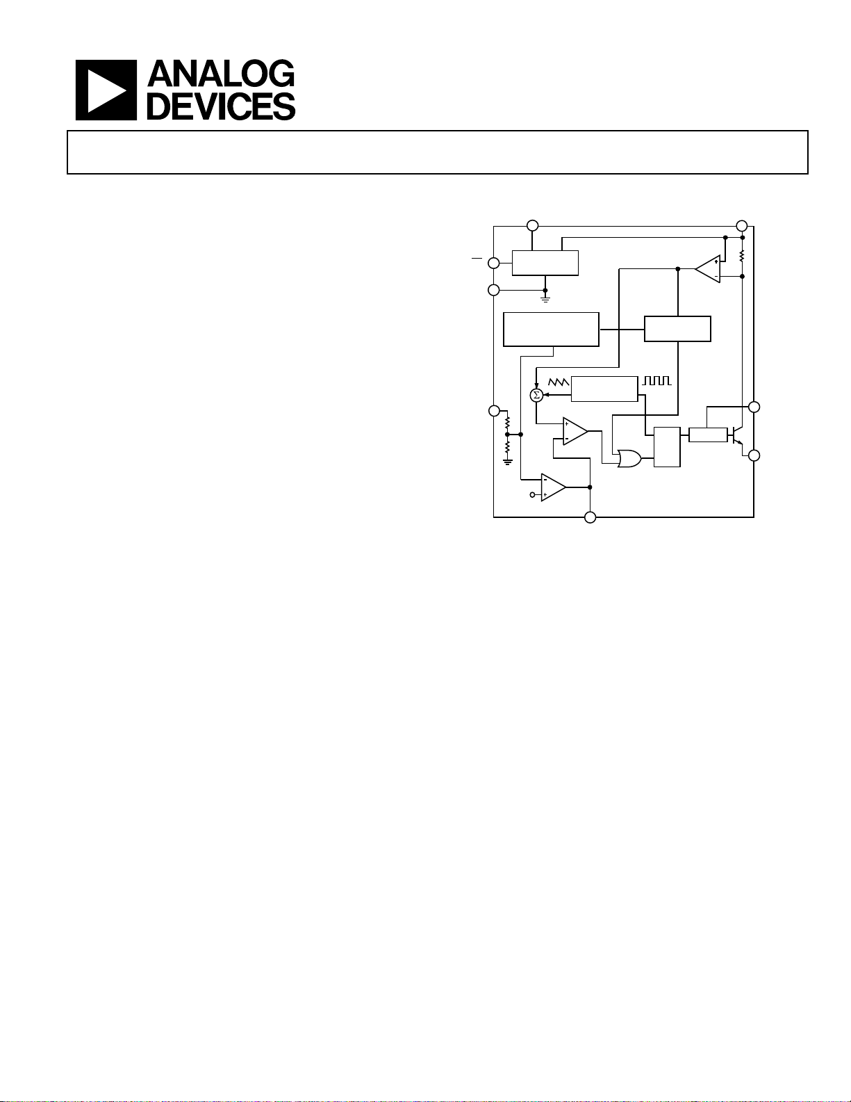
FUNCTIONAL BLOCK DIAGRAM
SD
GND
6
7
AND CURRENT LIMIT
4
FB
BIAS
3
2.50V
REGULATOR
FREQUENCY
FOLDBACK
+
1.2V
g
m
200kHz
OSCILLATOR
CMP
5
COMP
Figure 1.
CURRENT SENSE
AMPLIFIER
CURRENT
LIMIT
SQ
R
ADP3050
DRIVER
IN
8
BOOST
2
1
SWITCH
00125-001
GENERAL DESCRIPTION
The ADP3050 is a current mode monolithic buck (step down)
PWM switching regulator that contains a high current 1 A power
switch and all control, logic, and protection functions. It uses a
unique compensation scheme allowing the use of any type of
output capacitor (tantalum, ceramic, electrolytic, OS-CON).
Unlike some buck regulators, the design is not restricted to using
a specific type of output capacitor or ESR value.
A special boosted drive stage is used to saturate the NPN power
switch, providing a system efficiency higher than conventional
bipolar buck switchers. Further efficiency improvements are
obtained by using the low voltage regulated output to provide
the internal operating current of the device. A high switching
frequency allows the use of small external surface-mount components. A wide variety of standard off-the-shelf devices can be
used, providing a great deal of design flexibility. A complete
regulator design requires only a few external components.
Rev. B
Information furnished by Analog Devices is believed to be accurate and reliable. However, no
responsibility is assumed by Analog Devices for its use, nor for any infringements of patents or other
rights of third parties that may result from its use. Specifications subject to change without notice. No
license is granted by implication or otherwise under any patent or patent rights of Analog Devices.
Trademarks and registered trademarks are the property of their respective owners.
The ADP3050 includes a shutdown input that places the device
in a low power mode, reducing the total supply current to under
20 µA. Internal protection features include thermal shutdown
circuitry and a cycle-by-cycle current limit for the power switch
to provide complete device protection under fault conditions.
The ADP3050 provides excellent line and load regulation,
maintaining typically less than ±3% output voltage accuracy
over temperature and under all input voltage and output
current conditions.
The ADP3050 is specified over the industrial temperature range
of −40°C to +85°C and is available in a thermally enhanced 8-lead
(not Pb-free only) SOIC package and a standard 8-lead (Pb-free
only) RoHS-compliant SOIC package.
One Technology Way, P.O. Box 9106, Norwood, MA 02062-9106, U.S.A.
Tel: 781.329.4700 www.analog.com
Fax: 781.461.3113 ©2008 Analog Devices, Inc. All rights reserved.
Page 2

ADP3050
TABLE OF CONTENTS
Features .............................................................................................. 1
Applications ....................................................................................... 1
Functional Block Diagram .............................................................. 1
General Description ......................................................................... 1
Revision History ............................................................................... 2
Specifications ..................................................................................... 3
Absolute Maximum Ratings ............................................................ 4
ESD Caution .................................................................................. 4
Pin Configuration and Function Descriptions ............................. 5
Typical Performance Characteristics ............................................. 6
Theory of Operation ...................................................................... 10
Setting the Output Voltage ........................................................ 10
Applications Information .............................................................. 11
Inductor Selection ...................................................................... 11
Output Capacitor Selection ....................................................... 12
Catch Diode Selection ............................................................... 14
Input Capacitor Selection .......................................................... 14
Discontinous Mode Ringing ..................................................... 15
Setting the Output Voltage ........................................................ 15
Frequency Compensation ......................................................... 15
Current Limit/Frequency Foldback ......................................... 16
Bias Pin Connection .................................................................. 16
Boosted Drive Stage ................................................................... 16
Start-Up/Minimum Input Voltage ........................................... 16
Thermal Considerations ............................................................ 16
Board Layout Guidelines ............................................................... 18
Typical Applications ................................................................... 18
Inverting (Buck Boost) Regulator ............................................ 19
Outline Dimensions ....................................................................... 21
Ordering Guide .......................................................................... 21
REVISION HISTORY
3/08—Rev. A to Rev. B
Updated Format .................................................................. Universal
Changes to General Description Section ...................................... 1
Changes to Figure 3 and Figure 5 ................................................... 6
Changes to Table 2 ............................................................................ 4
Deleted Table 4 ................................................................................ 14
Changes to Table 5 .......................................................................... 15
Deleted Table 8 ................................................................................ 15
Deleted Table 7 ................................................................................ 16
Deleted Table 9 ................................................................................ 16
Changes to Boosted Drive Stage Section and Thermal
Considerations Sections ............................................................ 19
Changes to Figure 27 ...................................................................... 20
Changes to Ordering Guide .......................................................... 23
Rev. B | Page 2 of 24
Page 3

ADP3050
SPECIFICATIONS
VIN = 10 V, TA = −40°C to +85°C, unless otherwise noted.
Table 1.
Parameter1 Symbol Conditions Min Typ Max Unit
FEEDBACK
Feedback Voltage VFB Over line and temperature
ADP3050 1.16 1.20 1.24 V
ADP3050-3.3 3.20 3.30 3.40 V
ADP3050-5 4.85 5.00 5.15 V
Line Regulation VIN = 10 V to 30 V, no load 0.005 %/V
Load Regulation I
ADP3050AR-3.3, ADP3050AR-5 −0.5 +0.1 +0.5 %/A
Input Bias Current IFB ADP3050AR only 0.65 2 μA
ERROR AMPLIFIER
Transconductance
Voltage Gain
2
2
A
gm 1250 μMho
300 V/V
VOL
Output Current
ADP3050 COMP = 1.0 V, FB = 1.1 V to 1.3 V ±115 μA
ADP3050-3.3 COMP = 1.0 V, FB = 3.0 V to 3.6 V ±120 μA
ADP3050-5 COMP = 1.0 V, FB = 4.5 V to 5.5 V ±135 μA
OSCILLATOR
Oscillator Frequency3 f
Minimum Duty Cycle D
Maximum Duty Cycle D
170 200 240 kHz
OSC
10 %
MIN
90 %
MAX
SWITCH
Average Output Current Limit
4
I
CL(AVG)
ADP3050 BOOST = 15 V, FB = 1.1 V 1.0 1.25 1.5 A
ADP3050-3.3 BOOST = 15 V, FB = 3.0 V 1.0 1.25 1.5 A
ADP3050-5 BOOST = 15 V, FB = 4.5 V 1.0 1.25 1.5 A
Peak Switch Current Limit5 I
1.5 1.7 2.1 A
CL(PEAK)
Saturation Voltage BOOST = 15 V, I
Leakage Current 50 nA
SHUTDOWN
Input Voltage Low 0.4 V
Input Voltage High 2.0 V
SUPPLY
Input Voltage Range
Minimum BIAS Voltage V
Minimum BOOST Voltage V
6
VIN 3.6 30 V
3.0 V
BIAS
3.0 V
BOOST
IN Supply Current IQ
Normal Mode BIAS = 5.0 V 0.7 1.5 mA
Shutdown Mode
BIAS Supply Current I
BOOST Supply Current I
BIAS = 5.0 V 4.0 6.0 mA
BIAS
BOOST = 15 V, ISW = 0.5 A 18 mA
BOOST
BOOST = 15 V, ISW = 1.0 A 20 40 mA
1
All limits at temperature extremes are guaranteed via correlation using standard statistical quality control (SQC).
2
Transconductance and voltage gain measurements refer to the internal amplifier without the voltage divider. To calculate the transconductance and gain of the fixed
voltage parts, divide the values shown by FB/1.20.
3
The switching frequency is reduced when the feedback pin is lower than 0.8 × FB.
4
See Figure 24 for typical application circuit.
5
Switch current limit is measured with no diode, no inductor, and no output capacitor.
6
Minimum input voltage is not measured directly, but is guaranteed by other tests. The actual minimum input voltage needed to keep the output in regulation
depends on output voltage and load current.
= 100 mA to 1 A, ADP3050AR only −1.0 +0.1 +1.0 %/A
LOAD
= 1 A 0.65 0.95 V
LOAD
= 0 V, VIN ≤ 30 V
SD
15 40 μA
Rev. B | Page 3 of 24
Page 4
ADP3050
ABSOLUTE MAXIMUM RATINGS
Table 2.
Parameter Rating
IN Voltage
Continuous −0.3 V to +40 V
Peak (<100 ms) −0.3 V to +60 V
BOOST Voltage
Continuous −0.3 V to +45 V
Peak (<100 ms) −0.3 V to +65 V
SD, BIAS Voltage
FB Voltage −0.3 V to +8 V
COMP Voltage −0.3 V to IN + 0.3 V
SWITCH Voltage −0.3 V to IN + 0.3 V
Operating Ambient Temperature Range −40°C to +85°C
Operating Junction Temperature Range −40°C to +125°C
Storage Temperature Range −65°C to +150°C
θJA (4-Layer PCB)1 60.6°C/W
θJA (4-Layer PCB)2 87.5°C/W
Lead Temperature (Soldering, 60 sec) 300°C
1
Applied to all models that are not Pb-free.
2
Applied to all Pb-free models.
−0.3 V to IN + 0.3 V
Stresses above those listed under Absolute Maximum Ratings
may cause permanent damage to the device. This is a stress
rating only; functional operation of the device at these or any
other conditions above those indicated in the operational
section of this specification is not implied. Exposure to absolute
maximum rating conditions for extended periods may affect
device reliability.
ESD CAUTION
Rev. B | Page 4 of 24
Page 5
ADP3050
PIN CONFIGURATION AND FUNCTION DESCRIPTIONS
SWITCH
1
FB
ADP3050
2
3
TOP VIEW
(Not to Scale)
4
BOOST
BIAS
Figure 2. Pin Configuration
Table 3. Pin Function Descriptions
Pin No. Mnemonic Description
1 SWITCH
2 BOOST
Switch Node. This pin is the emitter of the internal NPN power switch. The voltage at this pin switches between
and approximately −0.5 V.
V
IN
Boost Pin. This pin is used to provide a boosted voltage (higher than V
switch. With the higher drive voltage, the power switch can be saturated, greatly reducing the switch power
losses.
3 BIAS
Bias Input Pin. Connect this pin to the regulated output voltage to maximize system efficiency. When this pin is
above 2.7 V, most of the ADP3050 operating current is taken from the output instead of the input supply. Leave
unconnected if not used.
4 FB
Feedback Pin. This feedback pin senses the regulated output voltage. Connect this pin directly to the output
(fixed output versions).
5 COMP
Compensation Node. This pin is used to compensate the regulator with an external resistor and capacitor. This
pin is also used to override the control loop. However, the voltage on this pin should not exceed 2 V, because
the pin is internally clamped to ensure a fast transient response. Use a pull-up resistor if this pin is to be pulled
higher than 2 V.
6
SD
Shutdown Pin. Use this pin to turn the device on and off. If this feature is not needed, tie this pin directly to IN.
7 GND Ground Pin. Connect this pin to local ground plane.
8 IN
Power Input. Connect this pin to the input supply voltage. An input bypass capacitor must be placed close to
this pin to ensure proper regulator operation.
8
7
6
5
IN
GND
SD
COMP
00125-002
) for the drive stage of the NPN power
IN
Rev. B | Page 5 of 24
Page 6
ADP3050
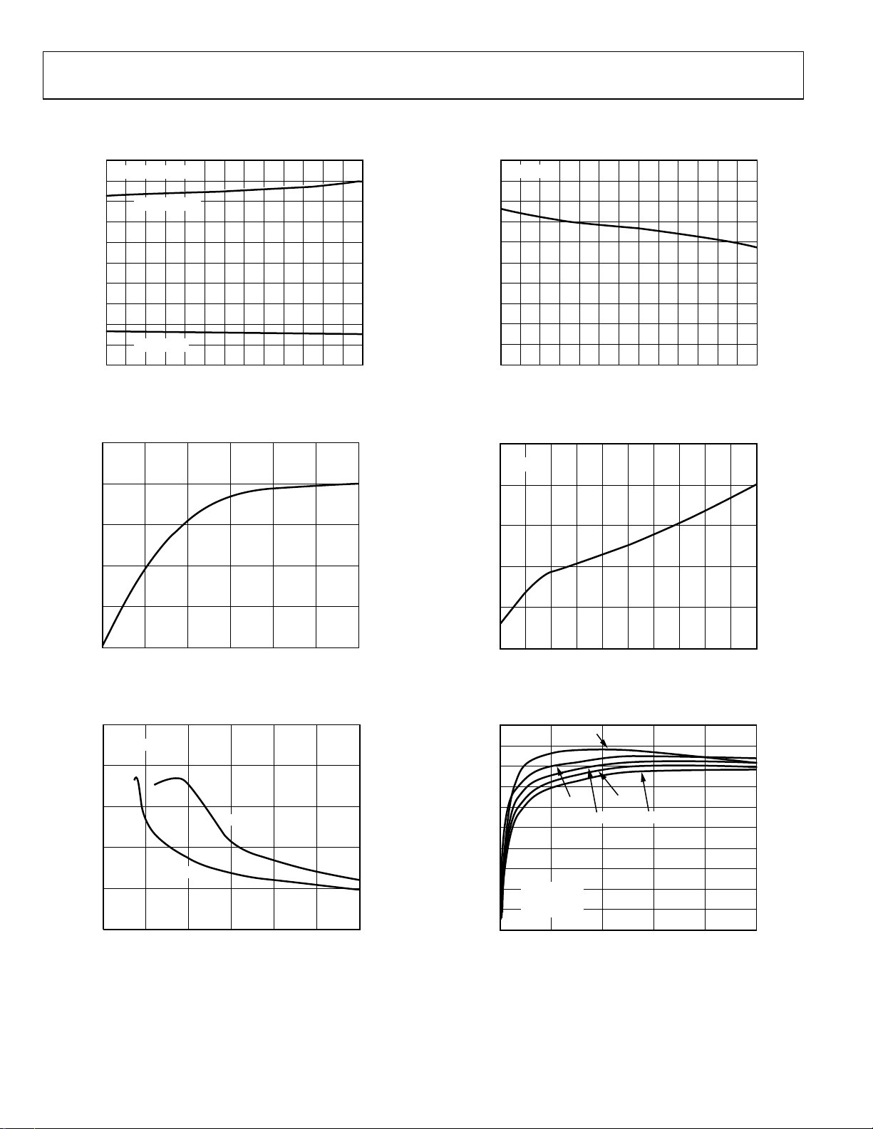
TYPICAL PERFORMANCE CHARACTERISTICS
5.0
VIN = 10V, NO L OAD
4.5
4.0
3.5
3.0
2.5
2.0
1.5
1.0
QUIESCENT O PERATING CURRENT (mA)
0.5
INTO BIAS PIN
INTO IN PIN
0
–45 –35
–25 –15 –5 5 15 25 35 45 55 65 75 85
TEMPERATURE ( °C)
Figure 3. Quiescent Operating Current vs. Temperature
25
20
15
10
2.0
VIN = 10V
1.8
1.6
1.4
1.2
1.0
0.8
0.6
0.4
AVERAGE OUTP UT CURRENT (A)
0.2
0
00125-003
–45 –35 –25 –15 –5 5 15 25 35 45 55 65 75 85
TEMPERATURE (° C)
00125-006
Figure 6. Average Output Current Limit vs. Temperature
25
VIN = 10V
20
15
10
5
SHUTDOWN QUI ESCENT CURRENT (µA)
0
5 10152025
SUPPLY VOLTAGE (V)
Figure 4. Shutdown Quiescent Current vs. Supply Voltage
10
BIAS TIED T O V
8
6
4
2
QUIESCENT O PERATING CURRENT (mA)
0
OUT
V
= 3.3V
OUT
SUPPLY VOLTAGE (V)
V
= 5V
OUT
Figure 5. Quiescent Operating Current vs. Supply Voltage
BOOST CURRENT (mA)
5
300
00125-004
0
0
0.1 0.2
0.3 0.4 0.5 0.6 0.7 0.8 0.9 1.0
LOAD CURRENT (A)
00125-007
Figure 7. Boost Current vs. Load Current
100
90
80
70
60
50
40
EFFICIE NCY (%)
30
20
10
300 5 10 15 20 25
00125-005
0
0 200 400 600 800
L = 33µH
C
= 22µF
IN
C
= 100µF
OUT
VIN = 6V
VIN = 24V
= 12V
V
IN
V
= 18V
IN
OUTPUT CURRENT (mA)
VIN = 30V
k1
00125-008
Figure 8. 5 V Output Efficiency
Rev. B | Page 6 of 24
Page 7

ADP3050
100
90
80
70
60
50
40
EFFICIENCY (%)
30
20
10
0
VIN = 12V
L = 33µH
C
= 22µF
IN
= 100µF
C
OUT
V
= 5V
IN
VIN = 24V
VIN = 18V
OUTPUT CURRENT (mA)
V
= 30V
N
Figure 9. 3.3 V Output Efficiency
0.5
VIN = 10V
0.4
I
= 1A
LOAD
0.3
0.2
0.1
0
–0.1
–0.2
–0.3
OUTPUT VO LTAGE CHANGE (%)
–0.4
–0.5
–45 –35 –25 –15 –5 5 15 25 35 45 55 65 75 85
TEMPERATURE ( °C)
Figure 10. Output Voltage Change vs. Temperature
0.6
V
= 5V
OUT
0.4
0.2
= 1A
I
0
0.2
OUTPUT VO LTAGE CHANGE (%)
0.4
0.6
0
LOAD
= 100mA
I
LOAD
10 20 30
INPUT VOLTAGE (V)
Figure 11. 5 V Output Voltage Change vs. Input Voltage
0.6
V
= 3.3V
OUT
0.4
0.2
I
= 100mA
0
0.2
OUTPUT VO LTAGE CHANGE (%)
0.4
1k0 200 400 600 800
00125-009
0.6
0
LOAD
= 1A
I
LOAD
10 20 30
INPUT VOLTAGE (V)
00125-012
Figure 12. 3.3 V Output Voltage Change vs. Input Voltage
8
7
V
= 5V
6
5
4
MINIMUM INPUT VOLTAGE (V)
3
2
0
00125-010
0.1 0.2 0.3 0.4 0.5 0.6 0.7 0.8 0.9 1. 0
OUT
V
= 3.3V
OUT
LOAD CURRENT (A)
00125-013
Figure 13. Minimum Input Voltage vs. Load Current
0
–0.02
–0.04
–0.06
–0.08
–0.10
–0.12
–0.14
OUTPUT VO LTAGE CHANGE (%)
–0.16
–0.18
00125-011
VIN = 10V
0
0.10.20.30.40.50.60.70.80.91.0
LOAD CURRENT(A)
0125-014
Figure 14. Load Regulation
Rev. B | Page 7 of 24
Page 8
ADP3050
A
A
0.8
0.7
0.6
VIN = 10V
VSW = 5V/DIV
0.5
0.4
0.3
0.2
SWITCH SATURATION VOLTAGE (V)
0.1
0
0.1 0.2 0.3 0.4 0.5 0.6 0.7 0.8 0.9 1.0
LOAD CURRENT (A)
Figure 15. Switch Saturation Voltage vs. Load Current
210
VIN = 10V
208
I
= 250µA
LOAD
206
204
202
200
198
196
194
SWITCHING FREQUENCY (kHz)
192
190
–45 –35 –25 –15 –5 5 15 25 35 45 55 65 75 85
AMBIENT TEM PERATURE (°C)
Figure 16. Switching Frequency vs. Temperature
0V
= 500mA/DIV
I
L
VIN = 10V
V
= 5V
OUT
I
= 800mA
0
00125-015
LOAD
L = 33µH
C
= 22µF
IN
C
= 100µF
OUT
TIME (1µs/DIV)
00125-018
Figure 18. Continuous Conduction Mode Waveforms
VSW = 5V/DIV
0V
I
= 500mA/DIV
L
VIN = 10V
= 5V
V
OUT
= 100mA
I
LOAD
L = 33µH
= 22µF
C
IN
= 100µF
C
OUT
0
0125-016
TIME (1µs/DIV)
00125-019
Figure 19. Discontinuous Conduction Mode Waveforms
250
200
150
100
SWITCHING FREQUENCY (kHz)
50
0
0
VIN = 10V
COMP = 0.4V
NORMALIZE D FEEDBACK VOLTAGE (V)
Figure 17. Frequency Foldback
1.00.2 0.4 0.6 0.8
00125-017
Rev. B | Page 8 of 24
V
= 200mV/DIV
5V
1A
0A
OUT
I
LOAD
VIN = 10V
= 5V
V
OUT
= 100mA TO 1A SW ITCHED
I
LOAD
L = 33µH
= 22µF
C
IN
= 100µF
C
OUT
TIME (400µ s/DIV)
00125-020
Figure 20. Transient Response
Page 9

ADP3050
VIN = 10V
= 5V
V
OUT
= 19Ω
R
LOAD
L = 33µH CO ILT RONICS
UP2B-330
= 22µF
C
IN
= 100µF
C
OUT
0V
0A
TIME (100µ s/DIV)
V
I
L
Figure 21. Start-Up from Shutdown
1500
VIN = 10V, NO LOAD
1450
1400
1350
1300
1250
1200
1150
TRANSCONDUCTANCE (µM ho)
1100
1050
1000
–45 –35
–25–15–5 5 1525354555657585
TEMPERATURE (° C)
Figure 22. Error Amplifier Transconductance vs. Temperature
= 1V/DIV
OUT
= 500mA/DIV
57.6
48.0
38.4
28.8
19.2
9.6
0
MAGNITUDE (d B)
–9.6
–19.2
–28.8
–38.4
1
00125-021
NO LOAD
1k 10k 100k
FREQUENCY (Hz)
Figure 23. Error Amplifier Gain
00125-022
220
200
180
160
140
120
100
80
60
40
20
1M100
PHASE (Degrees)
00125-023
Rev. B | Page 9 of 24
Page 10

ADP3050
V
THEORY OF OPERATION
The ADP3050 is a fixed frequency, current mode buck regulator.
Current mode systems provide excellent transient response, and
are much easier to compensate than voltage mode systems (refer to
Figure 1). At the beginning of each clock cycle, the oscillator
sets the latch, turning on the power switch. The signal at the
noninverting input of the comparator is a replica of the switch
current (summed with the oscillator ramp). When this signal
reaches the appropriate level set by the output of the error amplifier,
the comparator resets the latch and turns off the power switch. In
this manner, the error amplifier sets the correct current trip
level to keep the output in regulation. If the error amplifier
output increases, more current is delivered to the output; if it
decreases, less current is delivered to the output.
The current sense amplifier provides a signal proportional to
switch current to both the comparator and to a cycle-by-cycle
current limit. If the current limit is exceeded, the latch is reset,
turning the switch off until the beginning of the next clock
cycle. The ADP3050 has a foldback current limit that reduces
the switching frequency under fault conditions to reduce stress
to the IC and to the external components.
Most of the control circuitry is biased from the 2.5 V internal
regulator. When the BIAS pin is left open, or when the voltage
at this pin is less than 2.7 V, all of the operating current for the
ADP3050 is drawn from the input supply. When the BIAS pin is
above 2.7 V, the majority of the operating current is drawn from
this pin (usually tied to the low voltage output of the regulator)
instead of from the higher voltage input supply. This can provide
substantial efficiency improvements at light load conditions,
especially for systems where the input voltage is much higher
than the output voltage.
The ADP3050 uses a special drive stage allowing the power
switch to saturate. An external diode and capacitor provide a
boosted voltage to the drive stage that is higher than the input
supply voltage. Overall efficiency is dramatically improved by
using this type of saturating drive stage.
Pulling the
mode, shutting off all internal circuitry and reducing the supply
current to under 20 A.
SD
pin below 0.4 V puts the device in a low power
3.3
V
OUT
+
4kΩ
C4
100µF
R1
C2
1nF
00125-024
1N5818
12V
V
IN
L1
33µH
D1
1N4148
C3
220nF
+
C1
22µF
D2
1
SWITCH
BOOST
2
BIAS
3
FB
4
ADP3050-3.3
U1
GND
COMP
SD
IN
8
7
6
5
Figure 24. Typical Application Circuit
SETTING THE OUTPUT VOLTAGE
The output of the adjustable version (ADP3050AR and
ADP3050ARZ) can be set to any voltage between 1.25 V and 12 V
by connecting a resistor divider to the FB pin as shown in
Figure 25.
V
1N5817
GND
D1
V
⎛
R1R2
⎜
⎜
⎝
22µH
C3
0.22µF
C
F
D2
1N4148
5V
IN
+
Figure 25. Adjustable Output Application Circuit
OUT
−×= 1
2.1
L1
R2
21.5kΩ
R1
20kΩ
C1
2×10µF
CERAMIC
⎞
(1)
⎟
⎟
⎠
2.5V
V
OUT
C4
+
2×22µF
7.5kΩ
R
C
CERAMIC
C
C
4.7nF
1
SWITCH
2
BOOST
3
BIAS
4
FB
ADP3050
C2
0.01µF
U1
GND
SD
COMP
8
IN
7
6
5
00125-025
Rev. B | Page 10 of 24
Page 11

ADP3050
−
−
−
APPLICATIONS INFORMATION
The complete process for designing a step-down switching
regulator using the ADP3050 is provided in the following
sections. Each section includes a list of recommended devices.
These lists do not include every available device or manufacturer.
They contain only surface-mount devices. Equivalent throughhole devices can be substituted if needed. In choosing components,
keep in mind what is most important to the design, for example,
efficiency, cost, and size. These ultimately determine which components are used. It is also important to ensure that the design
specifications are clearly defined and reflect the worst-case
conditions. Key specifications include the minimum and
maximum input voltage, the output voltage and ripple, and the
minimum and maximum load current.
INDUCTOR SELECTION
The inductor value determines the mode of operation for the
regulator: continuous mode, where the inductor current flows
continuously; or discontinuous mode, where the inductor current
reduces to zero during every switch cycle. Continuous mode is
the best choice for many applications. It provides higher output
power, lower peak currents in the switch, inductor, and diode,
and a lower inductor ripple current, which means lower output
ripple voltage. Discontinuous mode allows the use of smaller
magnetics, but at a price: lower available load current and
higher peak and ripple currents. Designs with a high input
voltage or a low load current often operate in discontinuous
mode to minimize inductor value and size. The ADP3050 is
designed to work well in both modes of operation.
Continuous Mode
The inductor current in a continuous mode system is a triangular
waveform (equal to the ripple current) centered around a dc
value (equal to the load current). The amount of ripple current
is determined by the inductor value, and is usually between 20%
and 40% of the maximum load current. To reduce the inductor
size, ripple currents between 40% and 80% are often used in
continuous mode designs with a high input voltage or a low
output current. The inductor value is calculated using the
following equation:
VV
−
OUT
)(
MAXIN
L ××
= (2)
RIPPLE
Where
V
is the maximum input voltage, V
IN(MAX)
regulated output voltage, and
(200 kHz). The initial choice for the amount of ripple current
may seem arbitrary, but it serves as a good starting point for
finding a standard off-the-shelf inductor value, such as
10 H, 15 H, 22 H, 33 H, and 47 H. If a specific inductance
value is to be used, simply rearrange Equation 2 to find the
ripple current. For an 800 mA, 12 V to 5 V system, and a
V
1
fI
SW
OUT
V
)(
MAXIN
OUT
f
is the switching frequency
SW
is the
ripple current of 320 mA (40% of 800 mA) is chosen, the
inductance is
512
1
×
=L
0.32
×
5
=×
3
12
10200
H45.5
A 47 H inductor is the closest standard value that gives a ripple
current of about 310 mA. The peak switch current is equal to
the load current plus one-half the ripple current (this is also the
peak current for the inductor and the catch diode).
1
III
MAXOUTPKSW
RIPPLE
)()(
2
=+=+=
(3)
A95.0155.08.0
Pick an inductor with a dc (or saturation) current rating about 20%
larger than I
to ensure that the inductor is not running near
SW(PK)
the edge of saturation. For this example, 1.20 × 0.95 A = 1.14 A, use
an inductor with a dc current rating of at least 1.2 A. The maximum switch current is internally limited to 1.5 A, and this limit,
along with the ripple current, determines the maximum load
current the system can provide.
If the load current decreases to below one-half the ripple
current, the regulator operates in discontinuous mode.
Discontinuous Mode
For load currents less than approximately 0.5 A, discontinuous
mode operation can be used. This allows the use of a smaller
inductor, but the ripple current is much higher (which means a
higher output ripple voltage). If a larger output capacitor must
be used to reduce the output ripple voltage, the overall system
may take up more board area than if a larger inductor is used.
The operation and equations for the two modes are quite different,
but the boundary between these two modes occurs when the ripple
current is equal to twice the load current (when I
RIPPLE
= 2 × I
OUT
).
From this, Equation 2 is used to find the minimum inductor
value needed to keep the system in continuous mode operation
(solve for the inductor value with I
VV
)(
L ××
DIS
MAXIN
= (4)
×
2
OUT
OUT
1
fI
SW
RIPPLE
= 2 × I
V
OUT
V
).
OUT
)(
MAXIN
Using an inductor below this value causes the system to operate
in discontinuous mode. For a 400 mA, 24 V to 5 V system
524
1
≤
L
DIS
×
4.02
×
×
5
≤×
3
24
10200
H7.24
If the chosen inductor value is too small, the internal current
limit trips each cycle and the regulator has trouble providing the
necessary load current.
Rev. B | Page 11 of 24
Page 12

ADP3050
Inductor Core Types and Materials
Many types of inductors are currently available. Numerous core
styles along with numerous core materials often make the selection
process seem even more confusing. A quick overview of the
types of inductors available makes the selection process a little
easier to understand.
Open core geometries (bobbin core) are usually less expensive
than closed core geometries (toroidal core) and are a good choice
for some applications, but care must be taken when they are
used. In open core inductors, the magnetic flux is not completely
contained inside the core. The radiating magnetic field generates
electromagnetic interference (EMI), often inducing voltages
onto nearby circuit board traces. These inductors may not be
suitable for systems that contain very high accuracy circuits or
sensitive magnetics. A few manufacturers have semiclosed and
shielded cores, where an outer magnetic shield surrounds a
bobbin core. These devices have less EMI than the standard
open core and are usually smaller than a closed core.
Most core materials used in surface-mount inductors are either
powdered iron or ferrite. For many designs, material choice is
arbitrary, but the properties of each material should be recognized.
Ferrites have lower core losses than powdered iron, but the
lower loss means a higher price. Powdered iron cores saturate
softly (the inductance gradually reduces as current rating is
exceeded), whereas ferrite cores saturate much more abruptly
(the inductance rapidly reduces). Kool M® is one type of ferrite
that is specially designed to minimize core losses and heat
generation (especially at switching frequencies above 100 kHz),
but again, these devices are more expensive.
The winding dc resistance (DCR) of the inductor must not be
overlooked. A high DCR can decrease system efficiency by 2%
to 5% for lower output voltages at heavy loads. To obtain a
lower DCR means using a physically larger inductor, so a tradeoff in size and efficiency must be made. The power loss due to this
resistance is I
with an inductor DCR of 100 m, the winding resistance
dissipates
(0.82 A)
system of 64 mW/(3.3 V × 800 mA) = 2.4%. Typical DCR
values are between 10 m and 200 m.
Choosing an Inductor
Several considerations must be made when choosing an inductor:
cost, size, EMI, core and copper losses, and maximum current
rating. Use the following steps to choose an inductor that is
right for the system (refer to the calculations and descriptions
in the Inductor Selection section). Contact the manufacturers
for their full product offering, availability, and pricing. The
manufacturers offer many more values and package sizes to suit
numerous applications.
2
× DCR. For an 800 mA, 5 V to 3.3 V system
OUT
2
× 0.1 = 64 mW. This represents a power loss to the
1.
Choose a mode of operation, then calculate the inductor
value using the appropriate equation. For continuous mode
systems, a ripple current of 40% of the maximum load current
is a good starting point. The inductor value can then be
increased or decreased, if desired.
Calculate the peak switch current (this is the maximum
2.
current seen by the inductor). Make sure that the dc (or
saturation) current rating of the inductor is high enough
(around 1.2× the peak switch current). Inductors with dc
current ratings of at least 1 A should be used for all
designs. This provides a safety margin for start-up and
fault conditions where the inductor current is higher than
normal. If the current rating of an inductor is exceeded, the
core saturates, causing the inductance value to decrease
and the temperature of the inductor to increase.
Estimate the dc winding resistance based on the inductance
3.
value. A general rule is to allow approximately 5 m of
resistance per H of inductance.
Pick the core material and type. First, decide if an open-
4.
core inductor can be used with the design. If this cannot be
determined, try a few samples of each type (open core,
semi closed core, shielded core, and closed core). Do not be
discouraged from using open core inductors because they
require extra care; just be aware of what to look for if used.
They are quite small and inexpensive, and are used
successfully in many different applications.
OUTPUT CAPACITOR SELECTION
The ADP3050 can be used with any type of output capacitor.
The trade-offs between price, component size, and regulator
performance can be evaluated to determine the best choice for
each application. The effective series resistance (ESR) of the
capacitor plays an important role in both the loop compensation
and the system performance. The ESR provides a 0 in the
feedback loop; therefore, the ESR value must be known so the
loop can be compensated correctly (most manufacturers specify
maximum ESR in their data sheets). The capacitor ESR also
contributes to the output ripple voltage (V
RIPPLE
= ESR × I
Solid tantalum or multilayer ceramic capacitors are recommended,
providing good performance with a small size and reasonable cost.
Solid tantalum capacitors have a good combination of low ESR
and high capacitance, and are available from several different
manufacturers. Capacitance values from 22 F to more than 500 F
can be used, but values of 47 F to 220 F are sufficient for most
designs. A smaller value can be used, but ESR is size-dependent,
so a smaller device has a higher ESR. Ensure that the ripple
current of the capacitor rating is larger than the inductor ripple
current (the ripple current flows into the output capacitor).
RIPPLE
).
Rev. B | Page 12 of 24
Page 13

ADP3050
Multilayer ceramic capacitors can be used in applications where
minimum output voltage ripple is a priority. They have a very
low ESR (a 22 F ceramic can have an ESR one-fifth that of a
22 F solid tantalum), but may require more board area for the
same value of output capacitance. A few manufacturers have
recently improved upon their low voltage ceramic capacitors,
providing a smaller package with a lower ESR (NEC Tokin,
Murata, Taiyo Yuden, and AVX). Several ceramics can be used
in parallel to give an extremely low ESR and a good value of
capacitance. If the design is cost sensitive and not severely space
limited, several aluminum electrolytic capacitors can be used in
parallel (their size and ESR are larger than ceramic and solid
tantalum). OS-CON capacitors can also be used, but they are
typically larger and more expensive than ceramic or solid
tantalum capacitors.
Choosing an Output Capacitor
Use the following steps to choose an appropriate capacitor.
Decide the maximum output ripple voltage for the design,
1.
and this determines your maximum ESR (remember that
V
RIPPLE
≈ ESR × I
). Typical output ripple voltages range
RIPPLE
between 0.5% and 2% of the output voltage. To lower the
output voltage ripple, there are only two choices: either
increase the inductor value, or use an output capacitor with
a lower ESR.
Decide what type of capacitor to use (tantalum, ceramic, or
2.
others). Many more values, sizes, and voltage ratings are
available, so contact each manufacturer for a complete
product list. If a certain type of capacitor must be used and
space permits, use several devices in parallel to reduce the
total ESR.
Check the capacitor voltage rating and ripple current rating
3.
to ensure it works for the application in question. These
ratings are derated for higher temperatures, so always check
the manufacturer’s data sheet.
Make sure the final choice for the output capacitor has
4.
been optimized for cost, size, availability, and performance
yet still meets the required capacitance. The recommended
capacitance is in the 47 F to 220 F range.
Rev. B | Page 13 of 24
Page 14

ADP3050
Table 4. Manufacturers
Inductor Manufacturers Capacitor Manufacturers Schottky Diode Manufacturers
Sumida AVX
Coilcraft Kemet Diodes, Inc.
Cooper Bussmann Coiltronics Murata
NEC Tokin Nemco
Würth Elektronik
Toko
Vishay Sprague
NEC Tokin
Tai yo Yud en
CATCH DIODE SELECTION
The recommended catch diode is a Type 1N5818 Schottky or
equivalent. The low forward voltage drop (450 mV typical at
1 A) and fast switching speed of a Schottky rectifier provide the
best performance and efficiency. The 1N5818 is rated at 30 V
reverse voltage and 1 A average forward current. For lower
input voltages, use a lower voltage Schottky to reduce the diode
forward voltage drop and increase overall system efficiency; for
example, a 12 V to 5 V system does not need a 30 V diode. For
automotive applications, a 60 V Schottky may be necessary. The
average forward current for the catch diode is calculated by
VVII−
IN
OUT
)(
V
×=
OUT
AVGDIODE
For the earlier continuous mode example (12 V to 5 V at
800 mA), the average diode current is
512
−
8.0
I (6)
AVGDIODE
×=
)(
12
For this system, a 1N5817 is a good choice (rated at 20 V and 1 A).
Do not use catch diodes rated less than 1 A. Even though the
average current can be less than 1 A under normal operating
conditions, as the diode current is much higher under fault
conditions. The worst-case fault condition for the diode occurs
when the regulator becomes slightly overloaded (sometimes
called a soft short). This is usually only a problem when the
input voltage to output voltage ratio is greater than 2.5. Under
this condition, the load current needed is slightly more than the
regulator can provide. The output voltage droops slightly, and
the switch stays on every cycle until the internal current limit is
(5)
IN
A47.0
=
If the system must survive such gradual overloads for a prolonged
period of time, ensure the diode chosen can survive these
conditions. A larger 2 A or 3 A diode can be used if necessary.
Choosing a Catch Diode
Use the following steps to pick an appropriate catch diode.
Tabl e 5 shows several Schottky rectifiers with different reverse
voltage and forward current ratings.
The average diode current rating must be sufficient to provide
the required load current (see the calculations in the previous
section). Diodes rated below 1 A should not be used, even if the
average diode current is much lower.
The reverse voltage rating of the catch diode should be at least the
maximum input voltage. Often a higher rating is chosen
(1.2× the maximum input voltage) to provide a safety margin.
Table 5. Schottky Diode Selection Guide
VR 1 A 2 A 3 A
15 V 10BQ15 30BQ15
20 V 1N5817 B220 SK32
30 V V1N5818 B230
40 V 1N5819 B240 SK34
INPUT CAPACITOR SELECTION
The input bypass capacitor plays an important role in proper
regulator operation, minimizing voltage transients at the input
and providing a short local loop for the switching current. Place
this capacitor close to the ADP3050 between the IN and GND
pins using short, wide traces. This input capacitor should have
an rms ripple current rating of at least
reached. Under this condition, the load current can reach
around 1.2 A. For example, when using a system with an input
RMSCIN
voltage of 24 V and an output voltage of 5 V, if a gradual overload
causes the output voltage to droop to 4 V, the average diode
current is
424
−
2.1
I (7)
AVGDIODE
×=
)(
24
A0.1
=
This rating is crucial because the input capacitor must be able to
withstand the large current pulses present at the input of a stepdown regulator. Values of 20 F to 50 F are typical, but the
main criteria for capacitor selection is the ripple current and
voltage ratings.
Motorola
International Rectifier
Nihon Inter Electronics
2
⎞
⎛
OUT
V
V
II (8)
)(
OUT
IN
V
OUT
⎟
⎜
−×≥
⎟
⎜
V
IN
⎠
⎝
SK33
Rev. B | Page 14 of 24
Page 15

ADP3050
(
()(
Ceramics are an excellent choice for input bypassing, due to
their low ESR and high ripple current rating. Ceramics are
especially suited for high input voltages and are available from
many different manufacturers. Tantalums are often used for
input bypassing, but precautions must be taken because they
occasionally fail when subjected to large inrush currents during
power-up. These surges are common when the regulator input
is connected to a battery or high capacitance supply. Several
manufacturers now offer surface-mount solid tantalum capacitors
that are surge tested, but even these devices can fail if the current
surge occurs when the capacitor voltage is near its maximum
rating. For this reason, a 2:1 derating is suggested for tantalum
capacitors used in applications where large inrush currents are
present. For example, a 20 V tantalum should be used only for
an input voltage up to 10 V. Aluminum electrolytics are the
cheapest choice, but it takes several in parallel to get a good rms
current rating. OS-CON capacitors have a good ESR and ripple
current rating, but they are typically larger and more costly.
Refer to Table 4 for a list of capacitor manufacturers.
DISCONTINOUS MODE RINGING
When operating in discontinuous mode, high frequency
ringing appears at the switch node when the inductor current
has decreased to zero. This ringing is normal and is not a result
of loop instability. It is caused by the switch and diode capacitance
reacting with the inductor to form a damped sinusoidal ringing.
This ringing is usually in the range of several megahertz, and is
not harmful to normal circuit operation.
SETTING THE OUTPUT VOLTAGE
The fixed voltage versions of the ADP3050 (3.3 V and 5 V) have
the feedback resistor divider included on-chip. For the adjustable
version, the output voltage is set using two external resistors.
Referring to Figure 25, pick a value for R1 between 10 k and
20 k, then calculate the appropriate value for R2 using the
following equation:
V
⎛
R1R2 (9)
⎜
⎝
OUT
20.1
−×= 1
⎞
⎟
⎠
It is important to note that the accuracy of these resistors
directly affects the accuracy of the output voltage. The FB pin
threshold variation is ±3%, and the tolerances of R1 and R2 add
to this to determine the total output variation. Use 1% resistors
placed close to the FB pin to prevent noise pickup.
FREQUENCY COMPENSATION
The ADP3050 uses a unique compensation scheme that allows
the use of any type of output capacitor. The designer is not
limited to a specific type of capacitor or a specific ESR range.
External compensation allows the designer to optimize the loop
for transient response and system performance. The values for
R
and CC set the pole and zero locations for the error amplifier
C
to compensate the regulator loop.
For tantalum output capacitors, the typical system compensation
values are R
values are R
= 4 k and CC = 1 nF; for ceramics, the typical
C
= 4 k and CC = 4.7 nF. These values may not be
C
optimized for all designs, but they provide a good starting point for
selecting the final compensation values. Other types of output
capacitors require different values of C
between 0.5 nF and 10 nF.
C
Typically, the lower the ESR of the output capacitor, the larger
the value for C
. Normal variations in capacitor ESR, output
C
capacitance, and inductor value (due to production tolerances,
changes in operating point, changes in temperature) affect the
loop gain and phase response. Always check the final design
over its complete operating range to ensure proper regulator
operation.
Adjusting the R
and CC values can optimize compensation. Use
C
the typical values above as a starting point, then try increasing
and decreasing each independently and observing the transient
response. An easy way to check the transient response of the
design is to observe the output while pulsing the load current at
a rate of approximately 100 Hz to 1 kHz. There should be some
slight ringing at the output when the load pulses, but this should
not be excessive (just a few rings). The frequency of this ringing
shows the approximate unity-gain frequency of the loop. Again,
always check the design over its full operating range of input
voltage, output current, and temperature to ensure that the loop
is compensated correctly.
In addition to setting the zero location, R
also sets the high
C
frequency gain of the error amplifier. If this gain is too large,
output ripple voltage appears at the COMP pin (the output of
the error amplifier) with enough amplitude to interfere with
normal regulator operation. If this occurs, subharmonic switching
results (the pulsewidth of the switch waveform changes, even
though the output voltage stays regulated). The voltage ripple at the
COMP pin should be kept below 100 mV to prevent subharmonic
switching from occurring. The amount of ripple can be estimated
by the following formula, where g
transconductance (g
,
RIPPLECOMP
= 1250 Mho):
m
m
C
is the error amplifier
m
)( )
RIPPLE
ESRIRgV ××××=
V
FB
(10)
V
OUT
For example, a 12 V to 5 V, 800 mA regulator with an inductor of
L = 47 H has I
= 310 mA (see example from the Continuous
RIPPLE
Mode section) if a 100 F tantalum output capacitor with a
maximum ESR of 100 m and compensation values of R
= 1 nF are used. The ripple voltage at the COMP pin is
and C
C
V
,
RIPPLECOMP
=
−
mV2.37
If this ripple voltage is more than 100 mV, R
36
needs to be
C
C
)
1.0310.0104101250
××××××=
= 4 k
20.1
0.5
(11)
decreased to prevent subharmonic switching. Typical values for
are in the range of 2 k to 10 k.
R
C
Rev. B | Page 15 of 24
Page 16

ADP3050
V
V
+
(
)
(
)
×+×
=
For output voltages greater than 5 V, it may be necessary to add
a small capacitor in parallel with R2, as shown in Figure 25.
This improves stability and transient response. For tantalum
output capacitors, the typical value for C
output capacitors, the typical value for C
CURRENT LIMIT/FREQUENCY FOLDBACK
The ADP3050 uses a cycle-by-cycle current limit to protect the
device under fault and high stress conditions. When the current
limit is exceeded, the power switch turns off until the beginning
of the next oscillator cycle. If the voltage on the feedback pin
drops below 80% of its nominal value, the oscillator frequency
starts to decrease (see Figure 17 in the Typical Performance
Characteristics section). The frequency gradually reduces to a
minimum value of approximately 80 kHz (this minimum
occurs when the feedback voltage falls to 30% of its nominal
value). This reduces the power dissipation in the IC, the
external diode, and the inductor during short-circuit
conditions. This frequency foldback method provides complete
device fault protection without interfering with the normal
device operation.
is 100 pF. For ceramic
F
is 400 pF.
F
START-UP/MINIMUM INPUT VOLTAGE
For most designs, the regulated output voltage provides the
boosted voltage for the drive stage. During startup, the output
voltage is 0, so there is no boosted supply for the drive stage.
To deal with this problem, the ADP3050 contains a backup drive
stage to get everything started. As the output voltage increases,
so does the boost voltage. When the boost voltage reaches approximately 2.5 V, the switch drives transition smoothly from the
backup driver to the boosted driver. If the boost voltage decreases
below approximately 2.5 V, resulting in a short-circuit or
overload condition, the backup stage takes over to provide switch
drive. The minimum input voltage needed for the ADP3050 to
function correctly is about 3.6 V (this ensures proper operation of
the internal circuitry), but a small amount of headroom is
needed for all step-down regulators. The following formula gives
the approximate minimum input voltage needed for a given
system, where V
for the appropriate value of V
typical minimum input voltage needed for 3.3 V and 5 V
systems.
is the switch saturation voltage (see Figure 15
SAT
). Figure 13 also shows the
SAT
BIAS PIN CONNECTION
To help improve efficiency, most of the internal operating
current can be drawn from the lower voltage regulated output
voltage instead of the input supply. For example, if the input
voltage is 24 V and the output voltage is 5 V, a quiescent current
of 4 mA wastes 96 mW if drawn from the input supply, but only
20 mW is drawn from the regulated 5 V output. This power
savings is most evident at high input voltages and low load
currents. The output voltage must be 3 V or higher to take
advantage of this feature.
BOOSTED DRIVE STAGE
An external capacitor and diode are used to provide the boosted
voltage needed for the special drive stage. If the output voltage is
above 4 V, connect the anode of the boost diode to the regulated
output; for output voltages less than or equal to voltages of ≤3 V,
connect it to the input supply. For some low voltage systems,
such as 5 V to 3.3 V converters, the anode of the boost diode
can be connected to either the input or output voltage. During
switch off time, the boost capacitor is charged up to the voltage
at the anode of the boost diode. When the switch turns on, this
voltage is added to the switch voltage (the boost diode is reversebiased), providing a voltage higher than the input supply. The
peak voltage appearing on the BOOST pin is the sum of the
+ V
input voltage and the boost voltage (either V
IN
Ensure that this peak voltage does not exceed the BOOST pin
maximum rating of 45 V.
For most applications, a 1N4148 or 1N914 type diode can be
used with a 220 nF capacitor. A 470 nF capacitor may be needed
for output voltages between 3 V and 4 V. The boost capacitor
should have an ESR of less than 2 to ensure that it is
adequately charged up during switch off time. Almost any type
of film or ceramic capacitor can be used.
or 2 × VIN).
OUT
SATOUT
V
=
)(
MININ
(12)
85.0
THERMAL CONSIDERATIONS
Several factors contribute to IC power dissipation: ac and dc
switch losses, boost current, and quiescent current. The following
formulas are used to calculate these losses to determine the power
dissipation of the IC. These formulas assume continuous mode
operation, but they provide a reasonable estimate for discontinuous mode systems (do not use these formulas to calculate
efficiency at light loads).
Switch loss
⎛
⎜
⎜
⎝
VIP ×××+
SATOUT
SW
Boost current loss
I
P
BOOST
β
OUT
SW
Quiescent current loss
IN
Q
Q
where:
V
is ~0.6 V at I
SAT
f
is the switch frequency (200 kHz).
SW
t
is the switch current/voltage overlap time (~50 ns).
OV
β
is the current gain of the NPN power switch (~50).
SW
I
is the quiescent current drawn from VIN (~1 mA).
Q
I
is the quiescent current drawn from V
BIAS
OUT
⎞
V
OUT
⎟
××=
×= (14)
(
OV
⎟
V
IN
⎠
2
V
OUT
V
IN
OUT
OUT
IVIVP
(15)
BIAS
)
fVIt
IN
(13)
SW
= 800 mA (taken from Figure 15).
(~4 mA).
OUT
Rev. B | Page 16 of 24
Page 17

ADP3050
×+=
For example, a 5 V to 3.3 V system with I
⎛
P
⎜
SW
⎝
−
()
P
BOOST
()( )
P
Q
3.3
⎞
××=
6.08.0
+
⎟
0.5
⎠
2
3.3508.0
=×=
0.5
39
=×××××
mW35
33
−−
=××+×=
For a total IC power dissipation of
PPPP (16)
TOTAL
SW
BOOST
Q
The ADP3050 is offered in a thermally enhanced (not Pb-free)
8-lead SOIC package with a thermal resistance, θ
and in a standard Pb-free 8-lead SOIC package with θ
87.5°C/W.
The maximum die temperature, T
, is calculated using the
J
thermal resistance and the maximum ambient temperature
mW181043.3105
mW410=++=
= 800 mA
OUT
mW357102000.58.01050
JA
, of 60.6°C/W,
of
JA
PθTT
J
JAA
(17)
TOTAL
For the previous example (5 V to 3.3 V at 800 mA system, Pbfree 8-lead SOIC package using good layout techniques) with a
worst-case ambient temperature of 70°C
T
= 70°C + 87.5°C/W × 0.41 = 105.9°C
J
The maximum operating junction (die) temperature is 125°C,
therefore this system operates within the safe limits of the
ADP3050. Check the die temperature at minimum and
maximum supply voltages to ensure proper operation under all
conditions. Although the PCB and its copper traces provide
sufficient heat sinking, it is important to follow the layout
suggestions in the Board Layout Guidelines section. For any
design that combines high output current with high duty cycle
and/or high input voltage, the junction temperature must be
calculated to ensure normal operation. Always use the
equations in this section to estimate the power dissipation.
Rev. B | Page 17 of 24
Page 18

ADP3050
G
T
BOARD LAYOUT GUIDELINES
A good board layout is essential when designing a switching
regulator. The high switching currents along with parasitic
wiring inductances can generate significant voltage transients
and cause havoc in sensitive circuits. For best results, keep the
main switching path as tight as possible (keep L1, D1, C
C
close together) and minimize the copper area of the SWITCH
OUT
and BOOST nodes (without violating current density requirements) to reduce the amount of noise coupling into other
sensitive nodes.
V
IN
IN
SWITCH
L1
IN
, and
V
OUT
OUTPUT
GROUND
C1
L1
INPUT
C3
ADP3050
GND
C
D1
OUT
GND
0125-026
ND
C
IN
Figure 26. Main Switching Path
The external components should be located as close to the
ADP3050 as possible. For best thermal performance, use wide
copper traces for all IC connections, and always connect the
GND pin to a large piece of copper or ground plane. The additional
copper improves heat transfer from the IC, greatly reducing the
package thermal resistance. Further improvements of the thermal
performance can be made by using multilayer boards and using
vias to transfer heat to the other layers. A single layer board
layout is shown in Figure 27. The amount of copper used for the
input, output, and ground traces can be reduced, but were made
large to improve the thermal performance. For the 5 V and 3.3 V
versions, leave out R1 and R2; for the adjustable version, remove
the trace that shorts out R2. Route all sensitive traces and components, such as those associated with feedback and compensation,
away from the BOOST and SWITCH traces.
TYPICAL APPLICATIONS
5 V to 3.3 V Buck (Stepdown) Regulator
The circuit in Figure 28 shows the ADP3050 in a buck
configuration. It is used to generate 3.3 V regulated output from
5 V input voltage with the following specifications:
= 4.5 V to 5.5 V
V
IN
V
= 3.3 V
OUT
I
= 0.75 A
OUT
I
= 0.4 A × 0.75 A = 0.3 A
RIPPLE
V
OUT_RIPPLE
= 50 mV
D1
D2
R2 R1 CC RC
C2
ADP3050
00125-027
Figure 27. Recommended Board Layout
L1
1N5817
GND
22µH
D1
C3
0.22µF
1N4148
D2
1
SWITCH
2
BOOST
3
BIAS
4
FB
GND
SD
COMP
8
IN
7
6
5
U1
ADP3050-3.3
SD
5V
V
IN
+
C1
22µF
C2
0.01µF
Figure 28. 5 V to 3.3 V Buck Regulator
7.5kΩ
3.3V
V
OU
+
C5
100µF
R1
C4
1nF
00125-028
Rev. B | Page 18 of 24
Page 19

ADP3050
INVERTING (BUCK BOOST) REGULATOR
The circuit in Figure 29 shows the ADP3050 in a buck-boost
configuration that produces a negative output voltage from a
positive input voltage. This topology looks quite similar to the
buck shown in Figure 28 (except the IC and the output filter are
now referenced to the negative output instead of ground), but
its operation is quite different. For this topology, the feedback
pin is grounded and the GND pin is tied to the negative output,
allowing the feedback network of the IC to regulate the negative
output voltage.
47µH
1N5818
SD
12V
V
IN
GND
L1
D1
D2
1N4148
C3
0.22µF
+
C1
22µF
Figure 29. Inverting (Buck-Boost) Regulator
1
SWITCH
2
BOOST
3
BIAS
4
FB
U1
ADP3050-5
C2
0.01µF
GND
SD
COMP
8
IN
7
6
5
R1
5.1kΩ
C4
3.3nF
The design procedure used for the standard buck converter
cannot be used for a buck-boost converter due to fundamental
differences in how the output voltage is generated. The switch
currents in the buck-boost are much higher than the standard
buck converter, thus lowering the available load current. To
calculate the maximum output current for a given maximum
switch current, use the following equation:
V
I
MAXOUT
)(
⎡
I
⎢
⎢
⎣
where I
and V
IN
)(
MAXSW
is the switch current limit rating of the ADP3050,
SW(MAX)
is the minimum input voltage. The inductor ripple
IN
=
+
IN
−
2
×
VV
OUT
VV
×
IN
OUT
()
VVLf
+×××
SW
IN
(18)
⎤
⎥
⎥
OUT
⎦
current is estimated using the following equation:
100µF
C5
+
V
OUT
–5V AT 0.5A
00125-029
For the circuit in Figure 29, the maximum ripple current (at the
maximum input voltage) is
5
I
RIPPLE
12
=
−
1047
×
1
×
10200
×
−
×
36
=
512
−+
A375.0
High ripple currents are present in both the input and output
capacitors, and their ripple current ratings must be large
enough to sustain the large switching currents present in this
topology. The capacitors should have a ripple current rating of
at least
V
II
OUT
CCRMS
),(
IN
OUT
OUT
×≈
(20)
V
IN
The peak current seen by the diode, switch, and inductor is
found by rearranging the load current equation
I
PEAK
⎛
+
VV
IN
⎜
=
⎜
⎝
OUT
V
IN
⎞
1
⎛
⎟
×
OUT
×+
⎜
⎟
2
⎝
⎠
II
RIPPLE
⎞
(21)
⎟
⎠
The largest peak currents occur at the lowest input voltage. For
this design with a load current of 500 mA
512
−+
⎛
⎜
I (22)
=
PEAK
⎜
12
⎝
⎞
1
⎛
⎟
5.0
×
⎜
⎟
2
⎝
⎠
⎞
A9.0375.0
×+
=
⎟
⎠
The average current diode is equal to the load current.
An inductor with a current rating 20% greater than 0.9 A
should be used (a rating of at least 1.2 A). Inductors and diodes
with ratings greater than 1 A should always be used, even if
the calculated peak and average currents are lower. This ensures
that start-up and fault conditions do not overstress the
components.
For the buck-boost topology, the input voltage can be less than
the output voltage, such as V
= 4 V or V
IN
= −5 V, but the
OUT
available load current is even lower. The equations given in this
section are valid for input voltages less than and greater than
the output voltage. The voltage seen by the ADP3050 is equal to
the sum of the input and output voltages (the BOOST pin sees
the sum of V
+ 2 × |V
IN
|). It is important to ensure that the
OUT
maximum voltage rating of these pins is not exceeded.
I
RIPPLE
V
MAXIN
1
)(
fL
SW
V
××=
OUT
+
)(
MAXIN
(19)
VV
OUT
Rev. B | Page 19 of 24
Page 20

ADP3050
Dual Output SEPIC Regulator
For many systems, a dual polarity supply is needed. The circuit
in Figure 30 generates both a positive and a negative 5 V output
using a single magnetic component. The two inductors shown
are actually two separate windings on a single core contained in a
small, surface-mount package. The windings can be connected in
parallel or in series to be used as a single inductor for a conventional buck regulator, or they can be used as a 1:1 transformer,
as in this application. The first winding is used as the standard
buck inductor for the +5 V output. The second winding is used
to generate the −5 V output along with D2, C6, and C7.
+
L1*
25µH
+
L1*
25µH
D1
1N5818
*INDUCTOR IS A SINGLE CORE
WITH TW O WINDI NGS
COILTRONICS CTX25-4
SD
12V
V
IN
GND
C3
0.22µF
1N4148
+
C1
22µF
D3
C6
100µF
1
SWITCH
2
BOOST
3
BIAS
4
FB
ADP3050-5
C2
0.01µF
1N5818
GND
COMP
U1
Figure 30. Dual Output +5 V and −5 V Regulator
These components form a single-ended primary inductance
converter (SEPIC) using the 1:1 coupled inductor to generate
the negative supply. When the switch is off, the voltage across
the buck winding is equal to V
+ VD (VD is the diode drop).
O
This voltage is generated across the second winding, which is
C7
100µF
–5V AT 0.25A
V
+5V AT 0.5A
+
C5
100µF
R1
C4
1nF
OUT
V
OUT
0125-030
D2
8
IN
7
6
SD
5
5.1kΩ
connected to produce the −5 V supply. The −5 V output is
generated even without C6 in the circuit, but its inclusion
greatly improves the regulation of the negative output and
lowers the inductor ripple current. The total output current
available for both supplies is limited by the ADP3050 (internally
limited to around 1.0 A).
Keeping load currents below 500 mA and 250 mA, for the
positive and negative supplies, respectively, ensures that the
current limit is not reached under normal operation. These
limits are not interchangeable; 500 mA cannot be drawn from
the −5 V supply while drawing only 250 mA from the +5 V
supply. The maximum current available from the −5 V output is
directly related to the +5 V load current, due to the fact that the
+5 V output is used to regulate both supplies. Typically, the −5 V
load current should be around one-half of the +5 V load current
to ensure good regulation of both outputs. Additionally, the −5 V
output should have a preload (the minimum current level) of
1% to 2% of the +5 V load current. This helps maintain good
regulation of the −5 V output at light loads.
The ripple voltage of the +5 V output is that of a normal buck
regulator as described in the Applications Information section.
This ripple voltage is determined by the inductor ripple current
and the ESR of the output capacitor. For Figure 30, the positive
output voltage ripple is a 30 mV peak-to-peak triangular wave.
The ripple voltage of the −5 V output is a rectangular wave, due
to the rectangular shape of the current waveform into the −5 V
output capacitor. The amplitude of this current waveform is
approximately equal to twice the −5 V load current. For a load
current of 200 mA and an ESR of 100 mΩ, the negative output
voltage ripple is approximately 2 × 200 mA × 100 mΩ, or about
40 mV. The edges of this ripple waveform are quite fast. Along
with the inductance of the output capacitor, it generates narrow
spikes on the negative output voltage. These spikes can easily be
filtered out using an additional 5 μF to 10 μF bypass capacitor
close to the load (the inductance of the PCB trace and the
additional capacitor create a low-pass filter to remove these
high frequency spikes).
Rev. B | Page 20 of 24
Page 21

ADP3050
OUTLINE DIMENSIONS
5.00 (0.1968)
4.80 (0.1890)
4.00 (0.1574)
3.80 (0.1497)
0.25 (0.0098)
0.10 (0.0040)
COPLANARITY
0.10
CONTROLL ING DIMENSIONS ARE IN MILLI M E TERS; INCH DIMENSIONS
(IN PARENTHESES) ARE ROUNDED-OFF MILLIMETER EQUIVALENTS FOR
REFERENCE ON LY AND ARE NOT APPROPRIATE FOR USE IN DES IGN.
85
1
1.27 (0.0500)
SEATING
PLANE
COMPLIANT TO JEDEC STANDARDS MS-012-AA
BSC
6.20 (0.2441)
5.80 (0.2284)
4
1.75 (0.0688)
1.35 (0.0532)
0.51 (0.0201)
0.31 (0.0122)
8°
0°
0.25 (0.0098)
0.17 (0.0067)
0.50 (0.0196)
0.25 (0.0099)
1.27 (0.0500)
0.40 (0.0157)
45°
012407-A
Figure 31. 8-Lead Standard Small Outline Package [SOIC_N]
Narrow Body
(R-8)
Dimensions shown in millimeters and (inches)
ORDERING GUIDE
Ordering
Model Output Voltage Temperature Range1 Package Description Package Option
ADP3050AR ADJ −40°C to +85°C 8-Lead SOIC_N R-8 98
ADP3050AR-REEL ADJ −40°C to +85°C 8-Lead SOIC_N R-8 2,500
ADP3050AR-REEL7 ADJ −40°C to +85°C 8-Lead SOIC_N R-8 1,000
ADP3050AR-3.3 3.3 V −40°C to +85°C 8-Lead SOIC_N R-8 98
ADP3050AR-3.3-REEL 3.3 V −40°C to +85°C 8-Lead SOIC_N R-8 2,500
ADP3050AR-3.3-RL7 3.3 V −40°C to +85°C 8-Lead SOIC_N R-8 1,000
ADP3050AR-5 5 V −40°C to +85°C 8-Lead SOIC_N R-8 98
ADP3050AR-5-REEL 5 V −40°C to +85°C 8-Lead SOIC_N R-8 2,500
ADP3050AR-5-REEL7 5 V −40°C to +85°C 8-Lead SOIC_N R-8 1,000
ADP3050ARZ2 ADJ −40°C to +85°C 8-Lead SOIC_N R-8 98
ADP3050ARZ-RL
2
ADJ −40°C to +85°C 8-Lead SOIC_N R-8 2,500
ADP3050ARZ-R72 ADJ −40°C to +85°C 8-Lead SOIC_N R-8 1,000
ADP3050ARZ-3.32 3.3 V −40°C to +85°C 8-Lead SOIC_N R-8 98
ADP3050ARZ-3.3-RL2 3.3 V −40°C to +85°C 8-Lead SOIC_N R-8 2,500
ADP3050ARZ-3.3-RL72 3.3 V −40°C to +85°C 8-Lead SOIC_N R-8 1,000
ADP3050ARZ-52 5 V −40°C to +85°C 8-Lead SOIC_N R-8 98
ADP3050ARZ-5-REEL2 5 V −40°C to +85°C 8-Lead SOIC_N R-8 2,500
ADP3050ARZ-5-REEL72 5 V −40°C to +85°C 8-Lead SOIC_N R-8 1,000
1
Operating junction temperature is −40 to +125°C.
2
Z = RoHS Compliant Part.
Quantity
Rev. B | Page 21 of 24
Page 22

ADP3050
NOTES
Rev. B | Page 22 of 24
Page 23

ADP3050
NOTES
Rev. B | Page 23 of 24
Page 24

ADP3050
NOTES
©2008 Analog Devices, Inc. All rights reserved. Trademarks and
registered trademarks are the property of their respective owners.
D00125-0-5/08(B)
Rev. B | Page 24 of 24
 Loading...