

Page 1
V
Micropower Step-Up/Step-Down Fixed 3.3 V, 5 V, 12 V,
Adjustable High Frequency Switching Regulator
FEATURES
Operates at supply voltages from 2 V to 30 V
Works in step-up or step-down mode
Very few external components required
High frequency operation up to 400 kHz
Low battery detector on-chip
User-adjustable current limit
Fixed and adjustable output voltage
8-lead PDIP, 8-lead SOIC, and 14-lead TSSOP packages
Small inductors and capacitors
APPLICATIONS
Notebook, palmtop computers
Cellular telephones
Hard disk drives
Portable instruments
Pagers
GENERAL DESCRIPTION
The ADP3000 is a versatile step-up/step-down switching
regulator. It operates from an input supply voltage of 2 V to
12 V in step-up mode, and from 2 V to 30 V in step-down mode.
Operating in pulse frequency mode (PFM), the device consumes
only 500 µA, making it ideal for applications requiring low
quiescent current. It delivers an output current of 180 mA at
3.3 V from a 2 V input in step-up mode, and an output current
of 100 mA at 3 V from a 5 V input in step-down mode.
The ADP3000 operates at 400 kHz switching frequency. This
allows the use of small external components (inductors and
capacitors), making it convenient for space-constrained designs.
The auxiliary gain amplifier can be used as a low battery detector,
linear regulator, undervoltage lockout, or error amplifier.
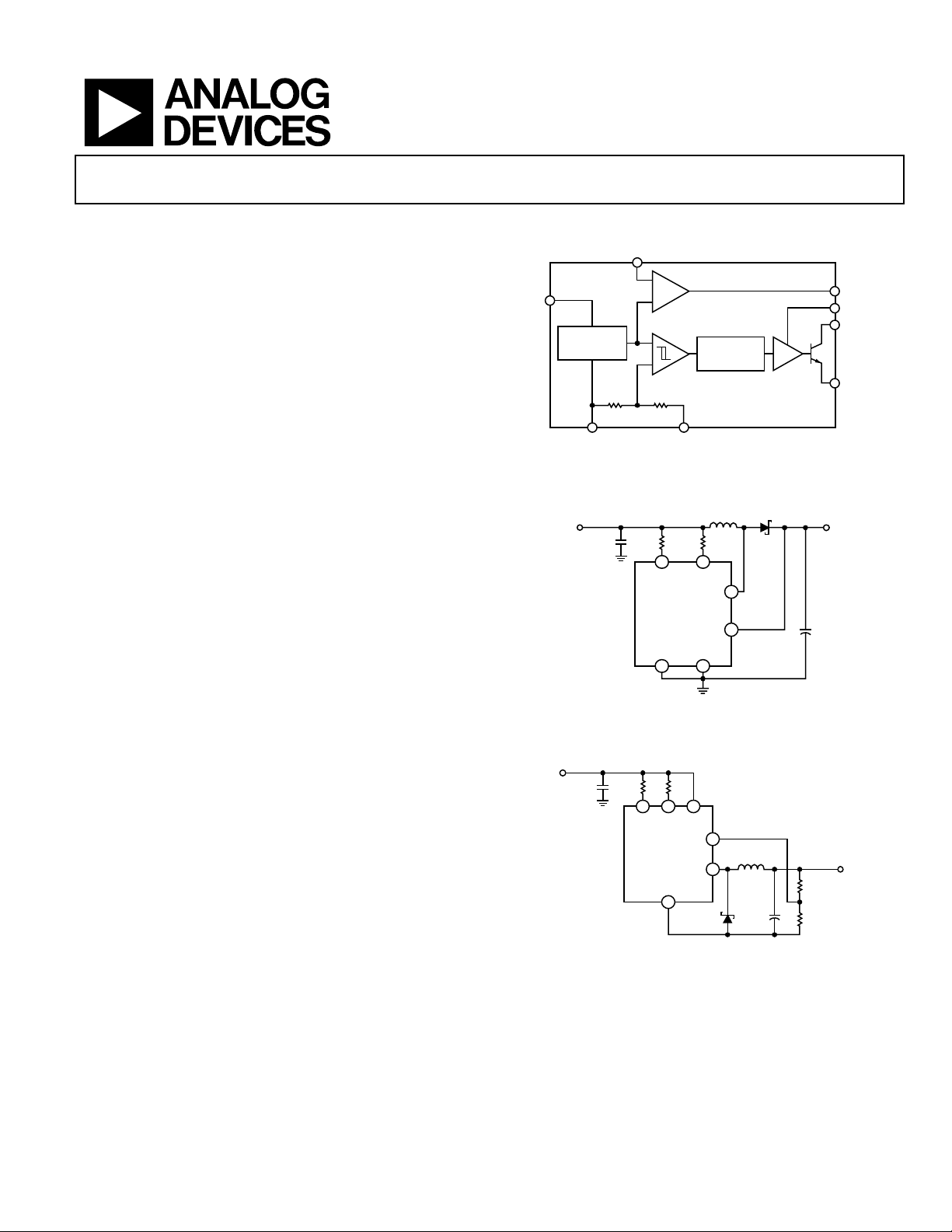
FUNCTIONAL BLOCK DIAGRAMS
IN
1.245V
REFERENCE
R1 R2
GND SENSE
V
IN
2V TO 3.2V
5V TO 6V
100µF
10V
V
IN
C1
100µF
120Ω
10V
C1, C2 = AVX TPS D107 M010R0100
L1 = SUMIDA CR43-100
Figure 3. Step-Down Mode Operation
SET
A1
GAIN BLOCK/
ERROR AMP
400kHz
OSCILLATOR
COMPARATOR
Figure 1.
6.8µH
120V
2
1
I
V
LIM
IN
SW1
ADP3000-3.3V
FB
(SENSE)
SW2GND
4
5
C1, C2 = AVX TPS D107 M010R0100
L1 = SUMIDA CR43-6R8
Figure 2. Typical Application
R
LIM
SW1
3
8
FB
1 2
I
LIMVIN
ADP3000
4
SW2
GND
5
D1
1N5818
3
8
ADP3000
DRIVER
ADP3000
IN5817
+
L1
10µH
C
L
+
100µF
10V
C1
100µF
10V
R2
150kΩ
1%
R1
110kΩ
1%
A0
I
LIM
SW1
SW2
3.3V
180mA
V
OUT
3V
100mA
00122-001
00122-002
00122-003
Rev. A
Information furnished by Analog Devices is believed to be accurate and reliable.
However, no responsibility is assumed by Analog Devices for its use, nor for any
infringements of patents or other rights of third parties that may result from its use.
Specifications subject to change without notice. No license is granted by implication
or otherwise under any patent or patent rights of Analog Devices. Trademarks and
registered trademarks are the property of their respective owners.
One Technology Way, P.O. Box 9106, Norwood, MA 02062-9106, U.S.A.
Tel: 781.329.4700 www.analog.com
Fax: 781.326.8703 © 2004 Analog Devices, Inc. All rights reserved.
Page 2

ADP3000
TABLE OF CONTENTS
Specifications..................................................................................... 3
Programming the Gain Block................................................... 11
Absolute Maximum Ratings............................................................ 4
ESD Caution.................................................................................. 4
Pin Configurations and Function Descriptions ........................... 5
Typical Performance Characteristics ............................................. 6
Theory of Operation ........................................................................ 9
Applications Information .............................................................. 10
Component Selection................................................................. 10
Programming the Switching Current Limit............................ 10
REVISION HISTORY
9/04—Data Sheet Changed from Rev. 0 to Rev. A
Added RU-14 Package .................................................Universal
Changes to Table 4.....................................................................10
Changes to Table 5.....................................................................10
Updated Outline Dimensions..................................................15
Changes to Ordering Guide.....................................................16
Power Transistor Protection Diode in Step-Down
Configuration ............................................................................. 11
Thermal Considerations............................................................ 11
Typical Application Circuits ......................................................... 13
Outline Dimensions....................................................................... 15
Ordering Guide .......................................................................... 16
1/97—Revision 0: Initial Version
Rev. A | Page 2 of 16
Page 3
ADP3000
SPECIFICATIONS
0°C ≤ TA ≤ +70°C, VIN = 3 V, unless otherwise noted.1
Table 1.
ADP3000
Parameter Conditions Symbol Min Typ Max Unit
INPUT VOLTAGE Step-up mode V
Step-down mode 30.0 V
SHUT-DOWN QUIESCENT CURRENT VFB > 1.43 V; V
COMPARATOR TRIP POINT VOLTAGE ADP3000
2
OUTPUT SENSE VOLTAGE ADP3000-3.3
> 1.1 × V
SENSE
1.20 1.245 1.30 V
3
V
IQ 500 µA
OUT
ADP3000-53 4.75 5.00 5.25 V
ADP3000-123 11.40 12.00 12.60 V
COMPARATOR HYSTERESIS ADP3000 8 12.5 mV
OUTPUT HYSTERESIS ADP3000-3.3 32 50 mV
ADP3000-5 32 50 mV
ADP3000-12 75 120 mV
OSCILLATOR FREQUENCY f
DUTY CYCLE VFB < V
SWITCH-ON TIME I
LIM
D 65 80 %
REF
tied to VIN, VFB= 0 t
SWITCH SATURATION VOLTAGE TA = +25°C V
Step-Up Mode VIN = 3.0 V, ISW = 650 mA 0.5 0.75 V
V
= 5.0 V, ISW = 1 A 0.8 1.1 V
IN
Step-Down Mode VIN = 12 V, ISW = 650 mA 1.1 1.5 V
FEEDBACK PIN BIAS CURRENT ADP3000 VFB = 0 V I
SET PIN BIAS CURRENT V
GAIN BLOCK OUTPUT LOW I
REFERENCE LINE REGULATION
= V
SET
= 300 µA, V
SINK
5 V ≤ V
2 V ≤ V
I
REF
= 1.00 V V
SET
≤ 30 V
IN
≤ 5 V
IN
GAIN BLOCK GAIN RL = 100 kΩ4 A
GAIN BLOCK CURRENT SINK V
CURRENT LIMIT 220 Ω from I
≤ 1 V I
SET
to VIN I
LIM
CURRENT LIMIT TEMPERATURE COEFFICIENT
SWITCH-OFF LEAKAGE CURRENT Measured at SW1 pin 1 10 µA
V
= 12 V, TA = +25°C
SW1
MAXIMUM EXCURSION BELOW GND TA = +25°C
I
≤ 10 µA, switch off
SW1
2.0 12.6 V
IN
3.135 3.3 3.465 V
OUT
350 400 450 kHz
OSC
1.5 2 2.55 µs
ON
SAT
160 330 nA
FB
200 400 nA
SET
0.15 0.4 V
OL
0.02 0.15 %/V
0.2 0.6 %/V
1000 6000 V/V
V
300 µA
SINK
400 mA
LIM
−0.3
−400 −350
%/°C
mV
1
All limits at temperature extremes are guaranteed via correlation using standard statistical methods.
2
This specification guarantees that both the high and low trip points of the comparator fall within the 1.20 V to 1.30 V range.
3
The output voltage waveform will exhibit a saw-tooth shape due to the comparator hysteresis. The output voltage on the fixed output versions will always be within
the specified range.
4
100 kΩ resistor connected between a 5 V source and the AO pin.
Rev. A | Page 3 of 16
Page 4
ADP3000
ABSOLUTE MAXIMUM RATINGS
Table 2.
Parameter Rating
Input Supply Voltage, Step-Up Mode 15 V
Input Supply Voltage, Step-Down Mode 36 V
SW1 Pin Voltage 50 V
SW2 Pin Voltage
Feedback Pin Voltage (ADP3000) 5.5 V
Switch Current 1.5 A
Maximum Power Dissipation 500 mW
Operating Temperature Range 0°C to +70°C
Storage Temperature Range
Lead Temperature (Soldering, 10 s) 300°C
Thermal Impedance
R-8 170°C/W
RU-14 150°C/W
N-8 120°C/W
ESD CAUTION
ESD (electrostatic discharge) sensitive device. Electrostatic charges as high as 4000 V readily
accumulate on the human body and test equipment and can discharge without detection. Although
this product features proprietary ESD protection circuitry, permanent damage may occur on devices
subjected to high energy electrostatic discharges. Therefore, proper ESD precautions are
recommended to avoid performance degradation or loss of functionality.
−0.5 V to V
−65°C to +150°C
IN
Stresses above those listed under Absolute Maximum Ratings
may cause permanent damage to the device. This is a stress
rating only; functional operation of the device at these or any
other conditions above those indicated in the operational
section of this specification is not implied. Exposure to
Absolute Maximum Rating conditions for extended periods
may affect device reliability.
Rev. A | Page 4 of 16
Page 5
ADP3000
V
V
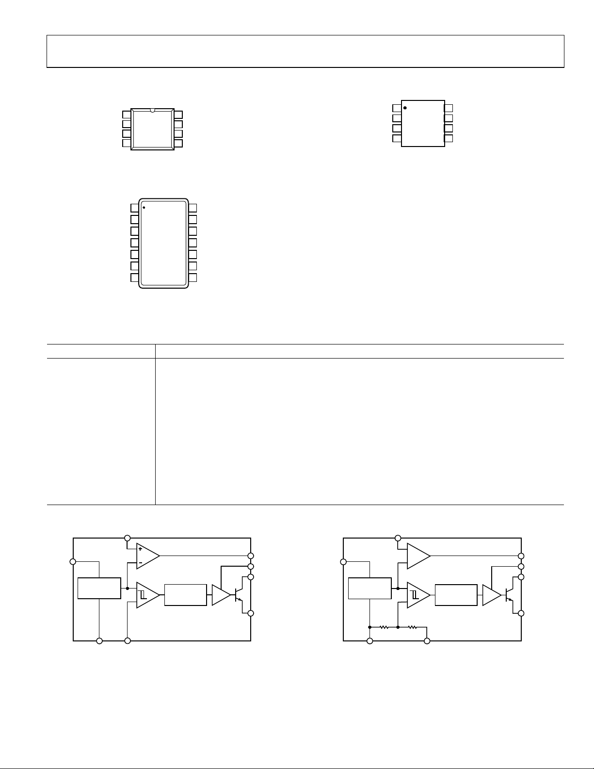
PIN CONFIGURATIONS AND FUNCTION DESCRIPTIONS
1
I
LIM
V
2
IN
SW1 3
SW2 4
*FIXED VERSIONS
ADP3000
TOP VIEW
(Not to Scale)
FB (SENSE)*8
SET7
6
AO
GND5
Figure 4. 8-Lead Plastic DIP (N-8)
1
NC
2
NC
3
ILIM
VIN
SW1
NC
SW2
ADP3000
4
TOP VIEW
(Not to Scale)
5
6
7
00122-004
14
NC
13
FB
12
SET
11
AO
NC
10
9
NC
8
GND
I
1
LIM
V
2
IN
ADP3000
SW1
3
TOP VIEW
(Not to Scale)
SW2
4
*FIXED VERSIONS
Figure 6. 8-Lead SOIC (R-8)
FB (SENSE)*
8
7
SET
6
AO
5
GND
00122-005
NC = NO CONNECT
00122-035
Figure 5. 14-lead TSSOP (RU-14)
Table 3. Pin Function Descriptions
Mnemonic Function
I
For normal conditions, connect to VIN. When lower current is required, connect a resistor between I
LIM
and VIN.
LIM
To limit the switch current to 400 mA, connect a 220 Ω resistor.
VIN
Input Voltage.
SW1 Collector of Power Transistor. For step-down configuration, connect to VIN. For step-up configuration, connect
to an inductor/diode.
SW2 Emitter of Power Transistor. For step-down configuration, connect to inductor/diode. For step-up
configuration, connect to ground. Do not allow pin to go more than a diode drop below ground.
GND Ground.
AO
Auxiliary Gain Block (GB) Output. Open collector can sink 300 µA. This pin can be left open if not used.
SET Auxiliary Gain Amplifier Input. The amplifier’s positive input is connected to the SET pin, and its negative
input is connected to the 1.245 V reference. This pin can be left open if not used.
FB/SENSE On the ADP3000 (adjustable) version, this pin is connected to the comparator input. On the ADP3000-3.3,
the ADP3000-5, and the ADP3000-12, the pin goes directly to the internal resistor divider that sets the
output voltage.
IN
1.245V
REFERENCE
SET
A2
A1
COMPARATOR
GAIN BLOCK/
ERROR AMP
OSCILLATOR
DRIVER
A0
I
LIM
SW1
SW2
IN
1.245V
REFERENCE
SET
A1
COMPARATOR
GAIN BLOCK/
ERROR AMP
OSCILLATOR
DRIVER
A0
I
LIM
SW1
SW2
ADP3000
GND
FB
Figure 7. Functional Block Diagram for Adjustable Version
00122-006
R1 R2
GND SENSE
ADP3000
Figure 8. Functional Block Diagram for Fixed Version
00122-007
Rev. A | Page 5 of 16
Page 6

ADP3000
TYPICAL PERFORMANCE CHARACTERISTICS
2.5
2.0
406
OSCILLATOR FREQUENCY
@ T
= 25°C
A
405
404
1.5
1.0
ON VOLTAGE (V)
0.5
0
VIN = 5V @ TA = 25°C
VIN = 3V @ TA = 25°C
VIN = 2V @ TA = 25°C
1.50.1 0.2 0.4 0.6 0.8 1.0 1.2 1.4
SWITCH CURRENT (A)
Figure 9. Switch-On Voltage vs. Switch Current in Step-Up Mode
1.4
1.2
1.0
0.8
(V)
0.6
CE(SAT)
V
0.4
0.2
0
VIN = 5V @ TA = 25°C
VIN = 12V @ TA = 25°C
0.90.1 0.2 0.3 0.4 0.5 0.6 0.8
SWITCH CURRENT (A)
Figure 10. Saturation Voltage vs. Switch Current in Step-Down Mode
00122-008
00122-009
403
402
401
400
OSCILLATOR FREQUENCY (kHz)
399
398
INPUT VOLTAGE (V)
Figure 12. Oscillator Frequency vs. Input Voltage
0.8
= 5V
V
IN
0.7
R
LIM
TA = 25°C
(Ω)
SWITCH CURRENT (A)
0.6
0.5
0.4
0.3
0.2
0.1
0
Figure 13. Maximum Switch Current vs. R
TA = 0°C
TA = 85°C
in Step-Down Mode (5 V)
LIM
30246810121518212427
00122-011
1k1 10 100
00122-A-012
QUIESCENT CURRENT (µA)
1400
1200
1000
800
600
400
200
QUIESCENT CURRENT @ TA = 25°C
0
INPUT VOLTAGE (V)
Figure 11. Quiescent Current vs. Input Voltage
301.5 3.0 6 9 12 15 18 21 24 27
00122-010
Rev. A | Page 6 of 16
1.8
SWITCH CURRENT (A)
1.6
1.4
1.2
1.0
0.8
0.6
0.4
0.2
V
= 12V
IN
TA = 85°C
0
TA = 25°C
R
(Ω)
LIM
Figure 14. Maximum Switch Current vs. R
TA = 0°C
in Step-Down Mode (12 V)
LIM
1k1 10 100
00122-013
Page 7

ADP3000
1.8
V
= 3V
IN
1.6
1.4
SWITCH CURRENT (A)
1.2
1.0
0.8
0.6
0.4
0.2
0
TA = 25°C
TA = 85°C
R
(Ω)
LIM
Figure 15. Maximum Switch Current vs. R
TA = 0°C
in Step-Up Mode (3 V)
LIM
1k1 10 100
00122-014
DUTY CYCLE (%)
100
90
80
70
60
50
40
30
20
10
0
TEMPERATURE (°C(TA))
85–40 0 25 70
00122-017
Figure 18. Duty Cycle vs. Temperature
OSCILLATOR FREQUENCY (kHz)
ON TIME (µs)
440
430
420
410
400
390
380
370
360
350
340
330
TEMPERATURE (°C(TA))
Figure 16. Oscillator Frequency vs. Temperature
2.30
2.25
2.20
2.15
2.10
2.05
2.00
1.95
1.90
1.85
1.80
TEMPERATURE (°C(TA))
Figure 17. Switch-On Time vs. Temperature
0.56
0.54
0.52
0.50
0.48
0.46
SATURATION VOLTAGE (V)
0.44
85–40 0 25 70
00122-015
0.42
TEMPERATURE (°C(TA))
VIN = 3V @ I
SW
= 0.65A
85–40 0 25 70
00122-018
Figure 19. Saturation Voltage vs. Temperature in Step-Up Mode
1.25
1.20
1.15
1.10
1.05
ON VOLTAGE (V)
1.00
0.95
85–40 0 25 70
00122-016
0.90
VIN = 12V @ I
TEMPERATURE (°C(TA))
SW
= 0.65A
85–40 0 25 70
00122-019
Figure 20. Switch-On Voltage vs. Temperature in Step-Down Mode
Rev. A | Page 7 of 16
Page 8

ADP3000
250
350
200
150
100
BIAS CURRENT (nA)
50
700
600
500
400
300
0
TEMPERATURE (°C(TA))
Figure 21. Feedback Bias Current vs. Temperature
VIN = 20V
300
250
200
150
100
BIAS CURRENT (nA)
50
85–40 0 25 70
00122-020
0
TEMPERATURE (°C(TA))
85–40 0 25 70
00122-022
Figure 23. Set Pin Bias Current vs. Temperature
200
QUIESCENT CURRENT (µA)
100
0
TEMPERATURE (°C(TA))
85–40 0 25 70
00122-021
Figure 22. Quiescent Current vs. Temperature
Rev. A | Page 8 of 16
Page 9

ADP3000
THEORY OF OPERATION
The ADP3000 is a versatile, high frequency, switch mode power
supply (SMPS) controller. The regulated output voltage can be
greater than the input voltage (in boost or step-up mode) or less
than the input voltage (in buck or step-down mode). This
device uses a gated oscillator technique to provide high
performance with low quiescent current.
An uncommitted gain block on the ADP3000 can be connected
as a low battery detector. The inverting input of the gain block
is internally connected to the 1.245 V reference. The
noninverting input is available at the SET pin. A resistor divider,
connected between V
and GND with the junction connected
IN
to the SET pin, causes the AO output to go low when the low
battery set point is exceeded. The AO output is an open
collector NPN transistor that can sink in excess of 300 µA.
Figure 7 is a functional block diagram of the ADP3000. The
internal 1.245 V reference is connected to one input of the
comparator, and the other input is externally connected (via the
FB pin) to a resistor divider, which is connected to the regulated
output. When the voltage at the FB pin falls below 1.245 V, the
400 kHz oscillator turns on. The ADP3000 internal oscillator
typically provides a 1.7 µs on time and a 0.8 µs off time. A driver
amplifier provides base drive to the internal power switch, and
the switching action raises the output voltage. When the voltage
at the FB pin exceeds 1.245 V, the oscillator shuts off. While the
oscillator is off, the ADP3000 quiescent current is only 500 µA.
The comparator’s hysteresis ensures loop stability without
requiring external components for frequency compensation.
The maximum current in the internal power switch is set by
connecting a resistor between V
and the I
IN
pin. When the
LIM
maximum current is exceeded, the switch is turned off. The
current limit circuitry has a time delay of about 0.3 µs. If an
external resistor is not used, connect I
maximum feasible current limit. Further information on I
to VIN. This yields the
LIM
LIM
is
included in the Applications Information section.
The ADP3000 provides external connections for both the
collector and the emitter of its internal power switch,
permitting both step-up and step-down modes of operation.
For the step-up mode, the emitter (Pin SW2) is connected to
GND, and the collector (Pin SW1) drives the inductor. For stepdown mode, the emitter drives the inductor, while the collector
is connected to V
.
IN
The output voltage of the ADP3000 is set with two external
resistors. Three fixed voltage models are also available:
ADP3000-3.3 (3.3 V), ADP3000-5 (5 V), and ADP3000-12
(12 V). The fixed voltage models include laser-trimmed,
voltage-setting resistors on the chip. On the fixed voltage
models of the ADP3000, simply connect the feedback pin
(Pin 8) directly to the output voltage.
Rev. A | Page 9 of 16
Page 10

ADP3000
APPLICATIONS INFORMATION
COMPONENT SELECTION
Inductor Selection
For most applications, the inductor used with the ADP3000
falls in the range of 4.7 µH to 33 µH. Table 4 shows
recommended inductors and their vendors.
When selecting an inductor for the ADP3000, it is very important
to make sure the inductor is able to handle a current higher than
the ADP3000’s current limit, without becoming saturated.
As a general rule, powdered iron cores saturate softly, whereas
Ferrite cores saturate abruptly. Rod and open drum core
geometry inductors saturate gradually. Inductors that saturate
gradually are easier to use. Even though rod and drum core
inductors are attractive in both price and physical size, they
must be used with care because they have high magnetic
radiation. When minimizing EMI is critical, toroid and closed
drum core geometry inductors should be used.
In addition, inductor dc resistance causes power loss. To
minimize power loss, it is best to use an inductor with a dc
resistance lower than 0.2 Ω.
Table 4. Recommended Inductors
Vendor Series Core Type Phone Number
Coiltronics OCTAPAC Toroid (561) 752-5000
Coiltronics UNIPAC Open (561) 752-5000
Sumida CR43, CR54 Open (847) 545-6700
Sumida
CDRH6D28,
CDRH73,
CDRH64
Capacitor Selection
For most applications, the capacitor used with the ADP3000
falls in the range of 33 µF to 220 µF. Table 5 shows
recommended capacitors and their vendors.
For input and output capacitors, use low ESR type capacitors for
best efficiency and lowest ripple. Recommended capacitors
include the AVX TPS series, the Sprague 595D series, the
Panasonic HFQ series, and the Sanyo OS-CON series.
When selecting a capacitor, it is important to make sure the
maximum capacitor ripple current rms rating is higher than the
ADP3000’s rms switching current.
It is best to protect the input capacitor from high turn-on
current charging surges by derating the capacitor voltage by 2:1.
For very low input or output voltage ripple requirements, use
capacitors with very low ESR, such as the Sanyo OS-CON
series. Alternatively, two or more tantalum capacitors can be
used in parallel.
Semi-Closed
Geometry
(847) 545-6700
Table 5. Recommended Capacitors
Vendor Series Type Phone Number
AVX TPS Surface Mount (843) 448-9411
Sanyo OS-CON Through Hole (619) 661-6835
Sprague 595D Surface Mount (603) 224-1961
Panasonic HFQ Through Hole (800) 344-2112
Diode Selection
The ADP3000’s high switching speed demands the use of
Schottky diodes. Suitable choices include the 1N5817, the
1N5818, the 1N5819, the MBRS120LT3, and the MBR0520LT1.
Fast recovery diodes are not recommended because their high
forward drop lowers efficiency. General-purpose and smallsignal diodes should be avoided as well.
PROGRAMMING THE SWITCHING CURRENT LIMIT
The ADP3000’s R
current limit to be programmed with a single external resistor.
This feature offers major advantages that ultimately decrease
the component’s cost and the PCB’s real estate. First, the R
pin allows the ADP3000 to use low value, low saturation current
and physically small inductors. Additionally, it allows for a
physically small surface-mount tantalum capacitor with a
typical ESR of 0.1 Ω. With this capacitor, it achieves an output
ripple as low as 40 mV to 80 mV, as well as a low input ripple.
The current limit is usually set to approximately 3 to 5 times the
full load current for boost applications, and about 1.5 to 3 times
the full load current in buck applications.
The internal structure of the I
Q1, the ADP3000’s internal power switch, is paralleled by sense
transistor Q2. The relative sizes of Q1 and Q2 are scaled so that
IQ2 is 0.5% of IQ1. Current flows to Q2 through both the R
resistor and an internal 80 Ω resistor. The voltage on these two
resistors biases the base-emitter junction of the oscillator-disable
transistor, Q3. When the voltage across R1 and R
Q3 turns on and terminates the output pulse. If only the 80 Ω
internal resistor is used (when the I
), the maximum switch current is 1.5 A. Figure 13, Figure 14,
V
IN
and Figure 15 give values for lower current limit levels.
V
IN
ADP3000
pin permits the cycle-by-cycle switch
LIM
circuit is shown in Figure 24.
LIM
LIM
pin is connected directly to
LIM
R
LIM
(EXTERNAL)
DRIVER
I
LIM
R1
80Ω
(INTERNAL)
I
Q1
200
Q2
SW1
SW2
Q1
POWER
SWITCH
V
IN
Q3
400kHz
OSCILLATOR
Figure 24. ADP3000 Current Limit Operation
LIM
LIM
exceeds 0.6 V,
00122-023
Rev. A | Page 10 of 16
Page 11

ADP3000
−
V
The delay through the current limiting circuit is approximately
0.3 µs. If the switch-on time is reduced to less than 1.7 µs,
accuracy of the current trip point is reduced as well. An attempt
to program a switch-on time of 0.3 µs or less produces spurious
responses in the switch-on time. However, the ADP3000 still
provides a properly regulated output voltage.
PROGRAMMING THE GAIN BLOCK
The ADP3000’s gain block can be used as a low battery detector,
an error amplifier, or a linear post regulator. It consists of an op
amp with PNP inputs and an open-collector NPN output. The
inverting input is internally connected to the 1.245 V reference,
and the noninverting input is available at the SET pin. The NPN
output transistor sinks in excess of 300 µA.
Figure 25 shows the gain block configured as a low battery
monitor. Set Resistors R1 and R2 to high values to reduce
quiescent current, but not so high that bias current in the SET
input causes large errors. A value of 33 kΩ for R2 is a good
compromise. The value for R1 is then calculated as follows:
V
LOBATT
R1
=
R2
where V
is the desired low battery trip point.
LOBATT
Because the gain block output is an open-collector NPN, a
pull-up resistor should be connected to the positive logic
power supply.
V
BATT
R2
33kΩ
Figure 25. Setting the Low Battery Detector Trip Point
The circuit of Figure 25 may produce multiple pulses when
approaching the trip point due to noise coupled into the SET
input. To prevent multiple interrupts to the digital logic, add
hysteresis to the circuit. Resistor R
10 MΩ, provides the hysteresis. The addition of R
trip point slightly, changing the new value for R1 to
V245.1
R1
V245.1−
ADP3000
1.245V
REF
SET
R1 =
V
LB
V
GND
R
1.6MΩ
V
– 1.245V
LB
37.7µA
= BATTERY TRIP POINT
HYS
5V
R
L
47kΩ
IN
AO
TO
PROCESSOR
HYS
00122-024
, with a value of 1 MΩ to
alters the
HYS
V
R1
=
LOBATT
⎛
R2
⎞
⎜
−
⎟
⎟
⎜
⎠
⎝
⎛
⎜
⎜
⎝
where:
is the logic power supply voltage.
V
L
is the pull-up resistor.
R
L
creates the hysteresis.
R
HYS
POWER TRANSISTOR PROTECTION DIODE IN STEP-DOWN CONFIGURATION
When operating the ADP3000 in step-down mode with the
switch off, the output voltage is impressed across the internal
power switch’s emitter-base junction. When the output voltage
is set to higher than 6 V, a Schottky diode must be placed in a
series with SW2 to protect the switch. Figure 26 shows the
proper way to place D2, the protection diode. The selection of
this diode is identical to the step-down commuting diode (refer
to the Diode Selection section).
IN
+
R3
C2
1 2
I
LIMVIN
ADP3000
GND
5
Figure 26. Step-Down Mode V
THERMAL CONSIDERATIONS
Power dissipation internal to the ADP3000 can be
approximated with the following equations.
Step-Up
⎡
⎢
D
SW
⎣
where:
is I
I
SW
otherwise, I
is the output voltage.
V
0
is the output current.
I
0
V
IN
when the current limit is programmed externally;
LIMIT
is the maximum inductor current.
SW
is the input voltage.
R is 1 Ω (typical R
D is 0.75 (typical duty ratio for a single switching cycle).
is 500 µA (typical shutdown quiescent current).
I
Q
β = 30 (typical forced beta).
2
RIP
+=
CE(SAT)
IN
).
V245.1
−
V
L
+
RR
L
D1, D2 = 1N5818 SCHOTTKY DIODES
3
SW1
8
FB
4
SW2
IV
⎡
⎤
SW
D
⎢
⎥
β
⎦
⎣
HYS
D2
D1
1
⎞
V245.1V245.1
⎟
⎟
⎠
L1
+
C1
> 6.0 V
OUT
⎡
⎤
4
V
IN
−
⎢
⎥
I
V
SW
O
⎣
⎦
R2
I
O
V
OUT
R1
⎤
[]
+
⎥
Q
⎦
> 6V
00122-025
[]
VI
IN
Rev. A | Page 11 of 16
Page 12

ADP3000
Step-Down
⎡
⎢
D
VIP
SW
CESAT
⎢
⎣
where:
is I
I
SW
otherwise, I
V
CE(SAT)
when the current limit is programmed externally;
LIMIT
is the maximum inductor current.
SW
is 1.2 V (typical value). Check this value by applying ISW
to Figure 10.
is the output voltage.
V
O
is the output current.
I
O
is the input voltage.
V
IN
D is 0.75 (typical duty ratio for a single switching cycle).
is 500 µA (typical shutdown quiescent current).
I
Q
β is 30 (typical forced beta).
The temperature rise can be calculated using the following
equation:
PT θ×=∆
D
JA
where:
∆T is temperature rise.
is device power dissipation.
P
D
is thermal resistance (junction-to-ambient).
θ
JA
⎡
⎛
⎞
1
⎜
+=
1
⎜
β
⎝
V
⎟
⎢
⎟
−
VV
⎢
IN
⎠
⎣
⎤
I
2
⎤
⎡
O
SATCE
O
⎥
⎥
)(
⎦
+
⎥
⎢
I
SW
⎦
⎣
[]
[]
VI
IN
Q
For example, consider a boost converter with the following
specifications:
⎤
⎥
⎥
V
is 2 V.
⎦
IN
is 3.3 V.
V
O
is 180 mA.
I
O
is 0.8 A (externally programmed).
I
SW
Using the step-up power dissipation equation:
⎡
)8.0)(2(
30
⎤
[]
⎥
⎦
⎡
2
18.0
D
⎢
⎣
+×= EP
2
⎤
⎡
−
175.0
⎢
⎣
⎢
⎥
3.3
⎦
⎣
∆T is 185 mW (170°C/W) = 31.5°C, using the R-8 package.
∆T is 185 mW (120°C/W) = 22.2°C, using the N-8 package.
At a 70°C ambient, the die temperature would be 101.45°C for
the R-8 package and 92.2°C for the N-8 package. These junction
temperatures are well below the maximum recommended
junction temperature of 125°C.
Finally, the die temperature can be decreased up to 20% by
using a large metal ground plate as ground pickup for the
ADP3000.
18.0)4(
⎤
[]
⎥
8.0
⎦
[]
26500
−+
Rev. A | Page 12 of 16
Page 13

ADP3000
2
TYPICAL APPLICATION CIRCUITS
3
SW1
FB
SW2
1N5817
GND
5
2
V
IN
SW1
SENSE
SW2GND
4
8
4
D1
SW1
SENSE
SW2
1N5817
15µH
3
L1
3
8
8
4
D1
L1
10µH
100µF
10V
IN5817
C2
+
10µH
L1
+
+
R2
150kΩ
R1
110kΩ
C2
100µF
10V
C2
100µF
16V
V
5V
250mA
V
OUT
12V
50mA
V
OUT
3V
100mA
OUT
00122-029
00122-031
V
IN
V TO 3.2V
100µF
10V
+
C1
ADP3000-3.3V
L1 = SUMIDA CR43-6R8
C1, C2 = AVX TPS D107 M010R0100
TYPICAL EFFICIENCY = 75%
Figure 27. 2 V to 3.3 V/180 mA Step-Up Converter
V
IN
2V TO 3.2V
100µF
10V
+
C1
ADP3000-5V
L1 = SUMIDA CR43-6R8
C1, C2 = AVX TPS D107 M010R0100
TYPICAL EFFICIENCY = 80%
Figure 28. 2 V to 5 V/100 mA Step-Up Converter
V
2.7V TO 4.5V
IN
+
C1
100µF
10V
L1 = SUMIDA CR43-6R8
C1, C2 = AVX TPS D107 M010R0100
TYPICAL EFFICIENCY = 80%
Figure 29. 2.7 V to 5 V/150 mA Step-Up Converter
120Ω
2
1
I
V
LIM
IN
SW1
SENSE
SW2GND
4
5
120Ω
2
1
I
V
LIM
IN
SW1
SENSE
SW2GND
4
5
120Ω
2
1
I
V
LIM
IN
SW1
ADP3000-5V
SENSE
SW2GND
4
5
L1
6.8µH
L1
6.8µH
L1
6.8µH
IN5817
3
8
V
OUT
3.3V
180mA
C2
+
100µF
10V
00122-026
V
4.5V TO 5.5V
IN
L1 = SUMIDA CR54-150
C1 = AVX TPS D107 M010R0100
C2 = AVX TPS D107 M016R0100
TYPICAL EFFICIENCY = 75%
100µF
10V
+
C1
124Ω
1
I
LIM
ADP3000-12V
5
Figure 30. 4.5 V to 12 V/50 mA Step-Up Converter
V
IN
IN5817
3
8
V
OUT
5V
100mA
C2
+
100µF
10V
00122-027
5V TO 6V
L1 = SUMIDA CR43-100
C1, C2 = AVX TPS D107 M010R0100
TYPICAL EFFICIENCY = 75%
100µF
10V
C1
120Ω
1 2
I
LIMVIN
ADP3000-ADJ
GND
5
Figure 31. 5 V to 3 V/100 mA Step-Down Converter
V
IN
C1
IN5817
3
8
V
OUT
5V
150mA
C2
+
100µF
10V
00122-028
10V TO 13V
L1: SUMIDA CR43-100
C1 = AVX TPS D336 M020R0200
C2 = AVX TPS D107 M010R0100
TYPICAL EFFICIENCY = 77%
33µF
20V
+
250Ω
1 2
I
LIMVIN
ADP3000-5V
Figure 32. 10 V to 5 V/250 mA Step-D own Converter
00122-030
Rev. A | Page 13 of 16
Page 14

ADP3000
2.5V TO 4.2V
AVX-TPS
100kΩ 120Ω
100µF
+
10V
90kΩ
1MΩ
V
IN
C1
47µF
16V
+
240Ω
1 2
I
LIMVIN
3
SW1
SENSE
8
5V
ADP3000-5V
4
L1 = SUMIDA CR54-150
C1 = AVX TPS D476 M016R0150
C2 = AVX TPS D107 M010R0100
TYPICAL EFFICIENCY = 60%
SW2
GND
5
1N5817
L1
15µH
D1
+
Figure 33. 5 V to −5 V/100 mA Inver ter
90kΩ
(SUMIDA – CDRH62)
6.8µH
1N5817
100µF
1%
1%
+
10V
AVX-TPS
348kΩ
200kΩ
I
LIMVIN
SET
ADP3000
A
0
GND
SW2
SW1
FB
330kΩ
2N2907
100kΩ 10kΩ
33nF
Figure 34. 1 Cell Li-Ion to 3 V/200 mA Conver ter with Shut-Down at V
C2
100µF
10V
V
OUT
–5V
100mA
00122-032
IN1
IN2
ADP3302AR1
SD
GND
≤ 2.5 V
IN
V
O1
V
O2
1µF
6V (MLC)
1µF
6V (MLC)
3V
100mA
3V
100mA
00122-033
@ V
≤ 2.5V
80
75
70
% EFFICIENCY
65
2.6 3.0 3.4 3.8 4.2
I
= 50mA + 50mA
O
I
= 100mA + 100mA
O
IN
SHDN IQ = 500µA
VIN
(V)
00122-034
Figure 35. Typical Efficiency of the Circuit of Figure 34
Rev. A | Page 14 of 16
Page 15

ADP3000
OUTLINE DIMENSIONS
0.375 (9.53)
0.365 (9.27)
0.355 (9.02)
8
1
0.100 (2.54)
0.180
(4.57)
MAX
0.150 (3.81)
0.130 (3.30)
0.110 (2.79)
0.022 (0.56)
0.018 (0.46)
0.014 (0.36)
CONTROLLING DIMENSIONS ARE IN INCHES; MILLIMETER DIMENSIONS
(IN PARENTHESES) ARE ROUNDED-OFF INCH EQUIVALENTS FOR
REFERENCE ONLY AND ARE NOT APPROPRIATE FOR USE IN DESIGN
COMPLIANT TO JEDEC STANDARDS MO-095AA
Figure 36. 8-Lead Plastic Dual In-Line Package [PDIP]
Dimensions shown in inches and (millimeters)
BSC
5
4
0.295 (7.49)
0.285 (7.24)
0.275 (6.98)
0.015
(0.38)
MIN
SEATING
PLANE
0.060 (1.52)
0.050 (1.27)
0.045 (1.14)
(N-8)
0.325 (8.26)
0.310 (7.87)
0.300 (7.62)
0.150 (3.81)
0.135 (3.43)
0.120 (3.05)
0.015 (0.38)
0.010 (0.25)
0.008 (0.20)
5.00 (0.1968)
4.80 (0.1890)
4.00 (0.1574)
3.80 (0.1497)
0.25 (0.0098)
0.10 (0.0040)
COPLANARITY
0.10
CONTROLLING DIMENSIONS ARE IN MILLIMETERS; INCH DIMENSIONS
(IN PARENTHESES) ARE ROUNDED-OFF MILLIMETER EQUIVALENTS FOR
REFERENCE ONLY AND ARE NOT APPROPRIATE FOR USE IN DESIGN
85
1.27 (0.0500)
SEATING
PLANE
COMPLIANT TO JEDEC STANDARDS MS-012AA
Figure 37. 8-Lead Standard Small Outline Package [SOIC]
Dimensions shown in millimeters and (inches)
BSC
6.20 (0.2440)
5.80 (0.2284)
41
1.75 (0.0688)
1.35 (0.0532)
0.51 (0.0201)
0.31 (0.0122)
Narrow Body
(R-8)
0.25 (0.0098)
0.17 (0.0067)
0.50 (0.0196)
0.25 (0.0099)
8°
1.27 (0.0500)
0°
0.40 (0.0157)
× 45°
Rev. A | Page 15 of 16
Page 16

ADP3000
5.10
5.00
4.90
1.05
1.00
0.80
4.50
4.40
4.30
PIN 1
14
0.65
BSC
0.15
0.05
COMPLIANT TO JEDEC STANDARDS MO-153AB-1
0.30
0.19
8
6.40
BSC
71
1.20
MAX
SEATING
PLANE
0.20
0.09
COPLANARITY
0.10
8°
0°
0.75
0.60
0.45
Figure 38. 14-Lead Thin Shrink Small Outline Package [TSSOP]
(RU-14)
Dimensions shown in millimeters
ORDERING GUIDE
Model Output Voltage Temperature Range Package Description Package Option
ADP3000AN Adjustable –40°C to +85°C 8-lead plastic DIP N-8
ADP3000AN-3.3 3.3 V –40°C to +85°C 8-lead plastic DIP N-8
ADP3000AN-5 5 V –40°C to +85°C 8-lead plastic DIP N-8
ADP3000AN-12 12 V –40°C to +85°C 8-lead plastic DIP N-8
ADP3000AR Adjustable –40°C to +85°C 8-lead SOIC R-8
ADP3000AR-REEL Adjustable –40°C to +85°C 8-lead SOIC R-8
ADP3000AR-3.3 3.3 V –40°C to +85°C 8-lead SOIC R-8
ADP3000AR-3.3-REEL 3.3 V –40°C to +85°C 8-lead SOIC R-8
ADP3000AR-5 5 V –40°C to +85°C 8-lead SOIC R-8
ADP3000AR-5-REEL 5 V –40°C to +85°C 8-lead SOIC R-8
ADP3000AR-12 12 V –40°C to +85°C 8-lead SOIC R-8
ADP3000AR-12-REEL 12 V –40°C to +85°C 8-lead SOIC R-8
ADP3000ARU Adjustable –40°C to +85°C 14-lead TSSOP RU-14
ADP3000ARU-REEL Adjustable –40°C to +85°C 14-lead TSSOP RU-14
© 2004 Analog Devices, Inc. All rights reserved. Trademarks and
registered trademarks are the property of their respective owners.
C00122–0–9/04(A)
Rev. A | Page 16 of 16
 Loading...