

Page 1
Step-Down DC-to-DC Regulator
ADP2441
Rev. 0
Information furnished by Analog Devices is believed to be accurate and reliable. However, no
Trademarks and registered trademarks are the property of their respective owners.
Fax: 781.461.3113 ©2012 Analog Devices, Inc. All rights reserved.
FB
COMP
EN
PGOOD
FREQ
SS/TRK
PGND
VIN
SW
BST
AGND
VCC
ADP2441
C4
C3
C
BST
C
IN
C
OUT
R
TOP
R
FREQ
R
COMP
C
COMP
R
BOTTOM
V
OUT
10581-001
V
OUT
V
IN
0
20
40
60
80
100
10
30
50
70
90
0.02 0.2 1
EFFICIENCY (%)
LOAD (A)
V
OUT
= 3.3V
10581-002
V
OUT
= 5V
V
OUT
= 12V
V
IN
= 24V
f
SW
= 300kHz
Data Sheet
FEATURES
Wide input voltage range of 4.5 V to 36 V
Low minimum on time of 50 ns
Maximum load current of 1 A
High efficiency of up to 94%
Adjustable output down to 0.6 V
±1% output voltage accuracy
Adjustable switching frequency of 300 kHz to 1 MHz
Pulse skip mode at light load for power saving
Precision enable input pin
Open-drain power good
External soft start with tracking
Overcurrent-limit protection
Shutdown current of less than 15 µA
UVLO and thermal shutdown
12-lead, 3 mm × 3 mm LFCSP package
APPLICAT ION S
Point of load applications
Distributed power systems
Industrial control supplies
Standard rail conversion to 24 V/12 V/5 V/3.3 V
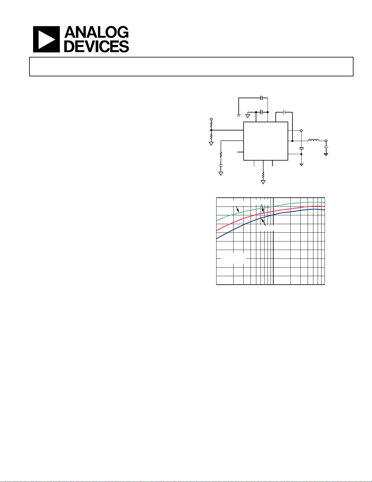
36 V,1 A, Synchronous,
TYPICAL CIRCUIT CONFIGURATION
Figure 1.
GENERAL DESCRIPTION
The ADP2441 is a constant frequency, current mode control,
synchronous, step-down dc-to-dc regulator that is capable of
driving loads up to 1 A with excellent line and load regulation
characteristics. The ADP2441 operates with a wide input voltage
range of 4.5 V to 36 V, which makes it ideal for regulating power
from a wide variety of sources. In addition, the ADP2441 has
very low minimum on time (50 ns) and is, therefore, suitable for
applications requiring a very high step-down ratio.
The output voltage can be adjusted from 0.6 V to 0.9 V × V
High efficiency is obtained with integrated low resistance
N-channel MOSFETs for both high-side and low-side devices.
The switching frequency is adjustable from 300 kHz to 1 MHz with
an external resistor. The ADP2441 also has an accurate power-good
(PGOOD) open-drain output signal.
At light load conditions, the regulator operates in pulse skip
mode by skipping pulses and reducing switching losses to improve
energy efficiency. In addition, at medium to heavy load conditions,
the regulator operates in fixed frequency pulse-width modulation
(PWM) mode to reduce electromagnetic interference (EMI).
responsibility is assumed by Analog Devices for its use, nor for any infringements of patents or other
rights of third parties that may result from its use. Specifications subject to change without notice. No
license is granted by implication or otherwise under any patent or patent rights of Analog Devices.
.
IN
The ADP2441 uses hiccup mode to protect the IC from short
circuits or from overcurrent conditions on the output. The external
programmable soft start limits inrush current during startup for
a wide variety of load capacitances. Other key features include
tracking, input undervoltage lockout (UVLO), thermal shutdown
(TSD), and precision enable (EN), which can also be used as a
logic level shutdown input.
The ADP2441 is available in a 3 mm × 3 mm, 12-lead LFCSP
package and is rated for a junction temperature range of −40°C
to +125°C.
One Technology Way, P.O. Box 9106, Norwood, MA 02062-9106, U.S.A.
Tel: 781.329.4700
Figure 2. Efficiency vs. Load Current, VIN = 24 V
www.analog.com
Page 2

ADP2441 Data Sheet
TABLE OF CONTENTS
Features .............................................................................................. 1
Applications ....................................................................................... 1
General Description ......................................................................... 1
Typical Circuit Configuration ......................................................... 1
Revision History ............................................................................... 2
Specifications ..................................................................................... 3
Absolute Maximum Ratings ............................................................ 5
Thermal Resistance ...................................................................... 5
ESD Caution .................................................................................. 5
Pin Configuration and Function Descriptions ............................. 6
Typical Performance Characteristics ............................................. 7
Internal Block Diagram ................................................................. 14
Theory of Operation ...................................................................... 15
Control Architecure ................................................................... 15
Adjustable Frequency ................................................................. 16
Power Good ................................................................................. 16
Soft Start ...................................................................................... 16
Tracking ....................................................................................... 16
Undervoltage Lockout (UVLO) ............................................... 17
Precision Enable/Shutdown ...................................................... 17
Current-Limit and Short-Circuit Protection .......................... 17
Thermal Shutdown ..................................................................... 17
Applications Information .............................................................. 18
Selecting the Output Voltage .................................................... 18
Setting the Switching Frequency .............................................. 18
Soft Start ...................................................................................... 19
External Components Selection ............................................... 19
Boost Capacitor .......................................................................... 21
VCC Capacitor............................................................................ 21
Loop Compensation .................................................................. 21
Large Signal Analysis of the Loop Compensation ................. 21
Design Example .............................................................................. 23
Configuration and Components Selection ............................. 23
System Configuration ................................................................ 24
Typical Application Circuits ......................................................... 25
Design Example .......................................................................... 25
Other Typical Circuit Configurations ..................................... 26
Power Dissipation and Thermal Considerations ....................... 29
Power Dissipation....................................................................... 29
Thermal Considerations ............................................................ 29
Evaluation Board Thermal Performance .................................... 30
Circuit Board Layout Recommendations ................................... 31
Outline Dimensions ....................................................................... 32
Ordering Guide .......................................................................... 32
REVISION HISTORY
6/12—Revision 0: Initial Version
Rev. 0 | Page 2 of 32
Page 3

Data Sheet ADP2441
Hysteresis
200 mV
Feedback Regulation Voltage
VFB
TJ = −40°C to +85°C
0.594
0.6
0.606
V
Leakage Current
I
VEN = AGND
1 25
μA
Peak Current Limit
ICL 1.4
1.6
1.8
A
Frequency Set Accuracy
FREQ pin = 308 kΩ
270
300
330
kHz
Hysteresis
V
100 mV
SPECIFICATIONS
VIN = 4.5 V to 36 V, TJ = −40°C to +125°C, unless otherwise noted.
Table 1.
Parameter Symbol Test Conditions/Comments Min Typ Max Unit
POWER SUPPLY
Input Voltage Range VIN 4.5 36 V
Supply Current I
Shutdown Current I
UVLO
Threshold V
INTERNAL REGULATOR
Regulator Output Voltage VCC VIN = 5 V to 36 V 5 5.5 V
OUTPUT
Output Voltage Range V
Maximum Output Current I
TJ = −40°C to +125°C 0.591 0.6 0.609 V
Line Regulation 0.005 %/V
Load Regulation 0.05 %/A
ERROR AMPLIFIER
Feedback Bias Current I
Transconductance gm I
Open-Loop Voltage Gain1 A
MOSFETS
High-Side Switch On Resistance2 R
Low-Side Switch On Resistance2 R
Minimum On Time3 t
Minimum Off Time
4
CURRENT SENSE
Current Sense Amplifier Gain GCS 1.6 2 2.4 A/V
Hiccup Time fSW = 300 kHz to1 MHz 6 ms
Number Of Cumulative Current-Limit Cycles
to Go into Hiccup Mode
VEN = 1.5 V not switching 1.7 2.2 mA
VIN
VEN = AGND 10 15 µA
SHDN
VIN falling 3.8 4 4.2 V
UVLO
0.6 0.9 × VIN V
OUT
1 A
OUT
VFB = 0.6 V 50 200 nA
FB_BIAS
= ±20 µA 200 250 300 µA/V
COMP
65 dB
VOL
BST − SW = 5 V 170 270 mΩ
DS_H(ON)
VCC = 5 V 120 180 mΩ
DS_L(ON)
LKG
All switching frequencies 50 65 ns
ON_MIN
t
165 175 ns
OFF_MIN
8 Events
FREQUENCY
Switching Frequency Range fSW 300 1000 kHz
FREQ pin = 92.5 kΩ 900 1000 1100 kHz
SOFT START
Soft Start Current ISS VSS = 0 V 0.9 1 1.2 µA
PRECISION ENABLE
Input Threshold V
Leakage Current I
Thermal Shutdown
Rising TSD 150 °C
Hysteresis T
1.15 1.20 1.25 V
EN(RISING)
EN(HYST )
VIN = VEN 0.1 1 µA
IEN_LEAK
25 °C
SD(HYST )
Rev. 0 | Page 3 of 32
Page 4

ADP2441 Data Sheet
PGOOD Low, FB Falling Threshold5
83
86
89
%
Parameter Symbol Test Conditions/Comments Min Typ Max Unit
POWER GOOD
PGOOD High, FB Rising Threshold5 89 92 95 %
PGOOD Low, FB Rising Threshold5 111 115 118 %
PGOOD High, FB Falling Threshold5 106 109 112 %
PGOOD
Delay t
High Leakage Current I
Pull-Down Resistor I
TRK
TRK Input Voltage Range 0 600 mV
TRK to FB Offset Voltage TRK = 0 mV to 500 mV 10 mV
1
Guaranteed by design.
2
Measured between VIN and SW pins—includes bond wires and pin resistance.
3
Based on bench characterization. Measured with VIN = 12 V, V
4
Based on bench characterization. Measured with VIN = 15 V, V
5
This threshold is expressed as a percentage of the nominal output voltage.
50 µs
PGOOD
V
PGOOD(SRC)
FB = 0 V 0.5 0.7 kΩ
PGOOD(SNK)
= 1.2 V, load = 1 A, fSW = 1 MHz, and the output in regulation. Measurement does not include dead time.
OUT
= 12 V, load = 1 A, fSW = 600 kHz, and the output in regulation. Measurement does not include dead time.
OUT
= VCC 1 10 µA
PGOOD
Rev. 0 | Page 4 of 32
Page 5
Data Sheet ADP2441
EN to AGND
−0.3 V to +40 V
ABSOLUTE MAXIMUM RATINGS
Table 2.
Parameter Rating
VIN to PGND −0.3 V to +40 V
SW to PGND −0.3 V to +40 V
BST to PGND −0.3 V to +45 V
VCC to AGND −0.3 V to +6 V
BST to SW −0.3 V to +6 V
FREQ, PGOOD, SS/TRK, COMP, FB to AGND −0.3 V to +6 V
PGND to AGND ±0.3 V
Operating Junction Temperature Range −40°C to +125°C
Storage Temperature Range −65°C to +150°C
Lead Temperature (Soldering, 10 sec) 260°C
Stresses above those listed under Absolute Maximum Ratings
may cause permanent damage to the device. This is a stress
rating only; functional operation of the device at these or any
other conditions above those indicated in the operational
section of this specification is not implied. Exposure to absolute
maximum rating conditions for extended periods may affect
device reliability.
THERMAL RESISTANCE
θJA is specified for the worst-case conditions, that is, a device
soldered in a circuit board for surface-mount packages, and is
based on a 4-layer standard JEDEC board.
Table 3. Thermal Resistance
Package Type θJA θJC Unit
12-Lead LFCSP 40 2.4 °C/W
ESD CAUTION
Rev. 0 | Page 5 of 32
Page 6
ADP2441 Data Sheet
FB
COMP
NOTES
1. THE EXPOSED PAD SHOULD BE CONNECTED
TO THE SYSTEMAGND P LANE AND PGND PLANE.
EN
VIN
SW
PGND
PGOOD
FREQ
SS/TRK
AGND
VCC
BST
10581-003
9
8
7
1
2
3
4
5
6
12
11
10
TOP
VIEW
ADP2441
PIN CONFIGURATION AND FUNCTION DESCRIPTIONS
Figure 3. Pin Configuration, Top View
Table 4. Pin Function Descriptions
Pin No. Mnemonic Description
1 FB Feedback Regulation Voltage is 0.6 V. Connect this pin to a resistor divider from the output of the dc-to-dc regulator.
2 COMP Error Amplifier Compensation. Connect a resistor and capacitor in series to ground.
3 EN Precision Enable. This features offers ±5% accuracy when using a 1.25 V reference voltage. Pull this pin high to
enable the regulator and low to disable the regulator.
4 PGOOD Active High Power-Good Output. This pin is pulled low when the output is out of regulation.
5 FREQ Switching Frequency. A resistor to AGND sets the switching frequency (see the Setting the Switching Frequency section).
6 SS/TRK Soft Start/Trac king Input. A capacitor to ground is required to program the soft start time, which gradually ramps
up the output. A resistive divider to an external reference is required on this pin to track an external voltage.
7 PGND Power Ground. Connect a decoupling ceramic capacitor as close as possible between the VIN pin and this pin.
Connect this pin directly to the exposed pad.
8 SW Switch. The midpoint for the drain of the low-side N-channel power MOSFET switch and the source for the high-side
N-channel power MOSFET switch.
9 VIN Power Supply Input. Connect this pin to the input power source, and connect a bypass ceramic capacitor directly
from this pin to PGND, as close as possible to the IC. The operation voltage is 4.5 V to 36 V.
10 BST Boost. Connect a 10 nF ceramic capacitor between the BST and SW pins as close to the IC as possible to form a
floating supply for the high-side N-Channel power MOSFET driver. This capacitor is needed to drive the gate of the
N-channel power MOSFET above the supply voltage.
11 VCC Output of the Internal Low Dropout Regulator. This pin supplies power for the internal controller and driver circuitry.
Connect a 1 µF ceramic capacitor between VCC and AGND and a 1 µF ceramic capacitor between VCC and PGND.
The VCC output is active when the EN pin voltage is more than 0.7 V.
12 AGND Analog Ground. This pin is the internal ground for the control functions. Connect this pin directly to the exposed pad.
EP Exposed Thermal Pad. The exposed pad should be connected to AGND and PGND.
Rev. 0 | Page 6 of 32
Page 7
Data Sheet ADP2441
0
20
40
60
80
100
10
30
50
70
90
0.01 0.1
LOAD (A)
1
EFFICIENCY (%)
V
IN
= 5V
V
IN
= 24V
V
OUT
= 3.3V
f
SW
= 300kHz
COILCRAF T MSS1038
VIN= 12V
10581-004
0
20
40
60
80
100
10
30
50
70
90
0.01 0.1 1
EFFICIENCY (%)
LOAD (A)
VIN = 12V
10581-006
VIN= 24V
VIN= 36V
V
OUT
= 5V
f
SW
= 300kHz
COILCRAF T MSS1038
0
20
40
60
80
100
10
30
50
70
90
0.01 0.1 1
EFFICIENCY (%)
LOAD (A)
VIN = 24V
10581-008
VIN= 36V
V
OUT
= 12V
f
SW
= 300kHz
COILCRAF T MSS1038
0
20
40
60
80
100
10
30
50
70
90
0.01 0.1 1
EFFICIENCY (%)
LOAD (A)
V
IN
= 5V
VIN= 12V
VIN= 24V
V
OUT
= 3.3V
f
SW
= 700kHz
COILCRAF T MSS1038
10581-005
0
20
40
60
80
100
10
30
50
70
90
0.01 0.1 1
EFFICIENCY (%)
LOAD (A)
VIN = 12V
10581-007
VIN= 36V
V
OUT
= 5V
f
SW
= 700kHz
COILCRAF T MSS1038
VIN= 24V
0
20
40
60
80
100
10
30
50
70
90
0.01 0.1 1
EFFICIENCY (%)
LOAD (A)
10581-009
V
OUT
= 12V
f
SW
= 600kHz
COILCRAF T MSS1038
VIN = 24V
VIN= 36V
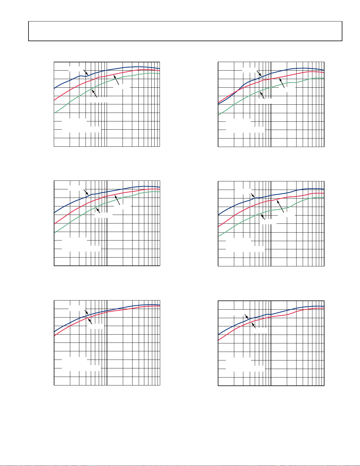
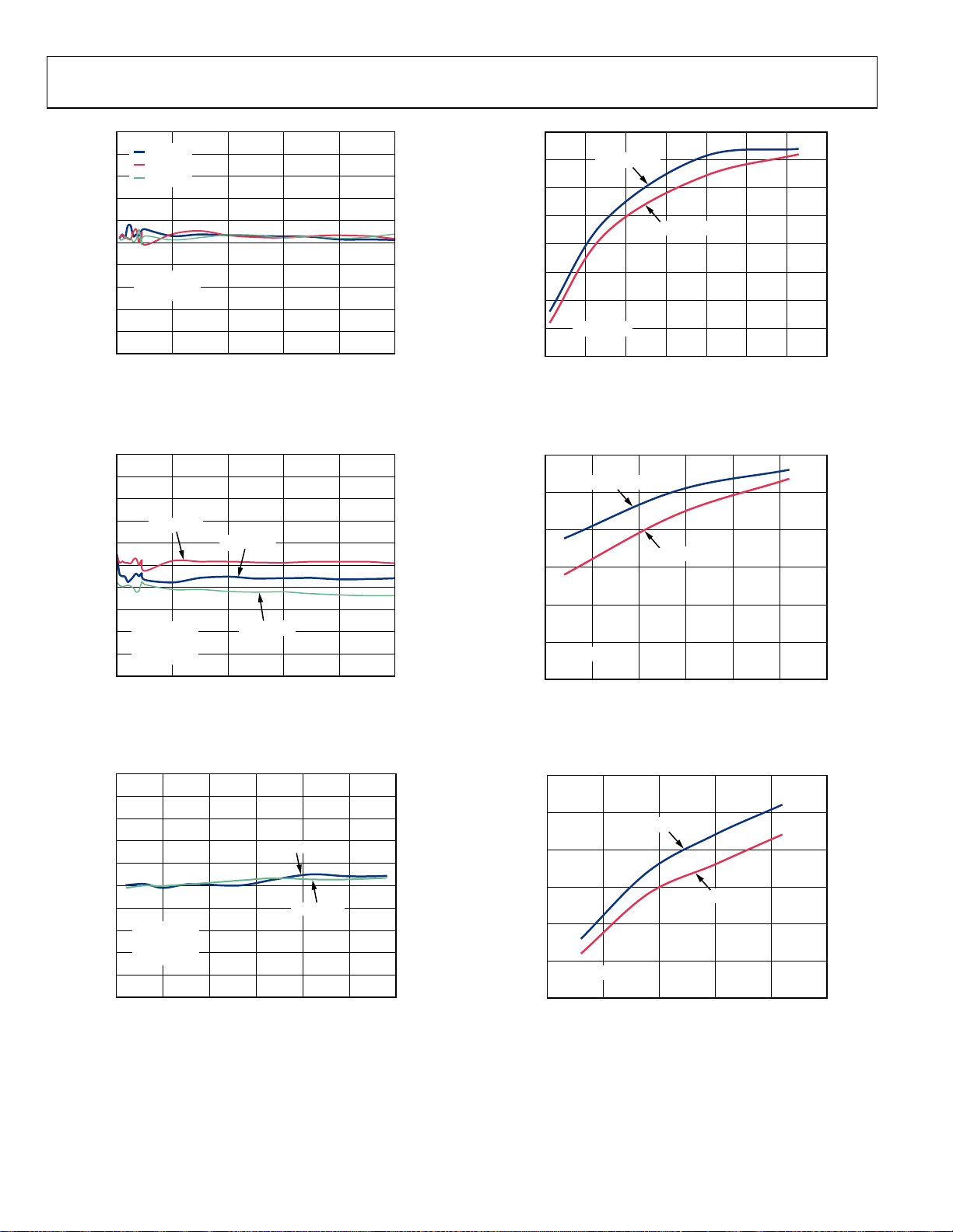
TYPICAL PERFORMANCE CHARACTERISTICS
Figure 4. Efficiency vs. Load Current,
V
= 3.3 V, fSW = 300 kHz
OUT
Figure 5. Efficiency vs. Load Current,
V
= 5 V, fSW = 300 kHz
OUT
Figure 7. Efficiency vs. Load Current,
V
= 3.3 V, fSW = 700 kHz
OUT
Figure 8. Efficiency vs. Load Current,
V
= 5 V, fSW = 700 kHz
OUT
Figure 6. Efficiency vs. Load Current,
V
= 12 V, fSW = 300 kHz
OUT
Figure 9. Efficiency vs. Load Current,
V
= 12 V, fSW = 600 kHz
OUT
Rev. 0 | Page 7 of 32
Page 8
ADP2441 Data Sheet
–0.5
–0.4
–0.3
–0.2
–0.1
0
0.1
0.2
0.3
0.4
0.5
0 0.2 0.4 0.6 0.8 1.0
V
OUT
ERROR (%)
LOAD (A)
V
IN
= 12V
V
IN
= 24V
V
IN
= 36V
V
OUT
= 5V
f
SW
= 700kHz
10581-010
1.0
0 0.2 0.4 0.6 0.8 1.0
V
OUT
ERROR (%)
LOAD (A)
T
A
= –40°C
T
A
= +25°C
T
A
= +125°C
10581-011
VIN= 24V
V
OUT
= 5V
f
SW
= 700kHz
–0.5
–0.4
–0.3
–0.2
–0.1
0
0.1
0.2
0.3
0.4
0.5
7 12 17 22 27 32 37
V
OUT
ERROR (%)
VIN (V)
LOAD = 500mA
LOAD = 1A
10581-012
VIN= 24V
V
OUT
= 5V
f
SW
= 700kHz
0
50
100
150
200
250
300
350
400
5 10 15 20 25 30 35 40
P
SKIP
THRESHOL D LOAD CURRENT (mA)
VIN (V)
f
SW
= 300kHz
f
SW
= 700kHz
V
OUT
= 3.3V
10581-013
0
50
100
150
200
250
300
10 15 20 25 30 35 40
P
SKIP
THRESHOL D LOAD CURRENT (mA)
VIN (V)
f
SW
=
700kHz
10581-014
V
OUT
= 5V
f
SW
=
300kHz
0
50
100
150
200
250
300
15 20 25 30 35 40
P
SKIP
THRESHOL D LOAD CURRENT (mA)
VIN (V)
f
SW
=
300kHz
f
SW
=
600kHz
10581-015
V
OUT
= 12V
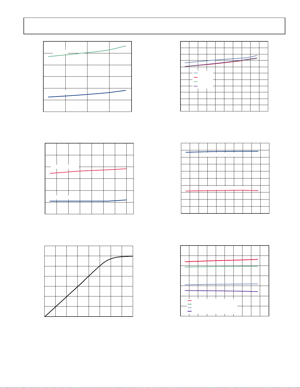
Figure 10. Load Regulation for Different Supplies
0.8
0.6
0.4
0.2
0
–0.2
–0.4
–0.6
–0.8
–1.0
Figure 13. Pulse Skip Threshold, V
OUT
= 3.3 V
Figure 11. Load Regulation for Different Temperatures
Figure 12. Line Regulation, V
OUT
= 5 V for Different Loads
Rev. 0 | Page 8 of 32
Figure 14. Pulse Skip Threshold, V
Figure 15. Pulse Skip Threshold, V
OUT
OUT
= 5 V
= 12 V
Page 9
Data Sheet ADP2441
0
2
4
8
6
10
12
–50 0 50 100 150
SHUTDOWN CURE NT (µA)
TEMPERATURE (°C)
V
IN
= 36V
V
IN
= 4.5V
10581-017
UVLO THRE S HOLD (V)
TEMPERATURE (°C)
10581-018
3.9
4.0
4.1
4.2
4.3
4.4
4.5
–50 –25 0 25 50 75 100 125
UVLO, RISING V
IN
UVLO, FALLING V
IN
0
0.1
0.2
0.3
0.4
0.5
0.6
0.7
0 0.1 0.2 0.3 0.4 0.5 0.6 0.7 0.8
FB (V)
TRACK (V)
10581-118
0.05
0.25
0.45
0.65
0.85
1.05
1.25
1.45
1.65
1.85
2.05
2.25
–50 –30 –10 10 30 50 70 90 110 130 150
SUPPLY CURRENT ( mA)
TEMPERATURE (°C)
V
IN
= 36V
V
IN
= 24V
V
IN
= 12V
V
IN
= 4.5V
10581-016
1.04
1.06
1.08
1.10
1.12
1.14
1.16
1.18
1.20
1.22
1.24
–50 –30 –10 10 30 50 70 90 110 130 150
ENABLE VOLTAGE (V)
TEMPERATURE (°C)
ENABLE RISING THRESHOLD
ENABLE FALLING THRESHOLD
10581-019
60
70
80
90
100
110
120
130
–50 –30 –10 10 30 50 70 90 110 130 150
PGOOD THRESHOLD (%)
TEMPERATURE (°C)
P
GOOD
RISE, F B INCREASING
P
GOOD
FALL, FB INCREASING
P
GOOD
RISE, F B DE CRE AS ING
P
GOOD
FALL, FB DECREASING
10581-021
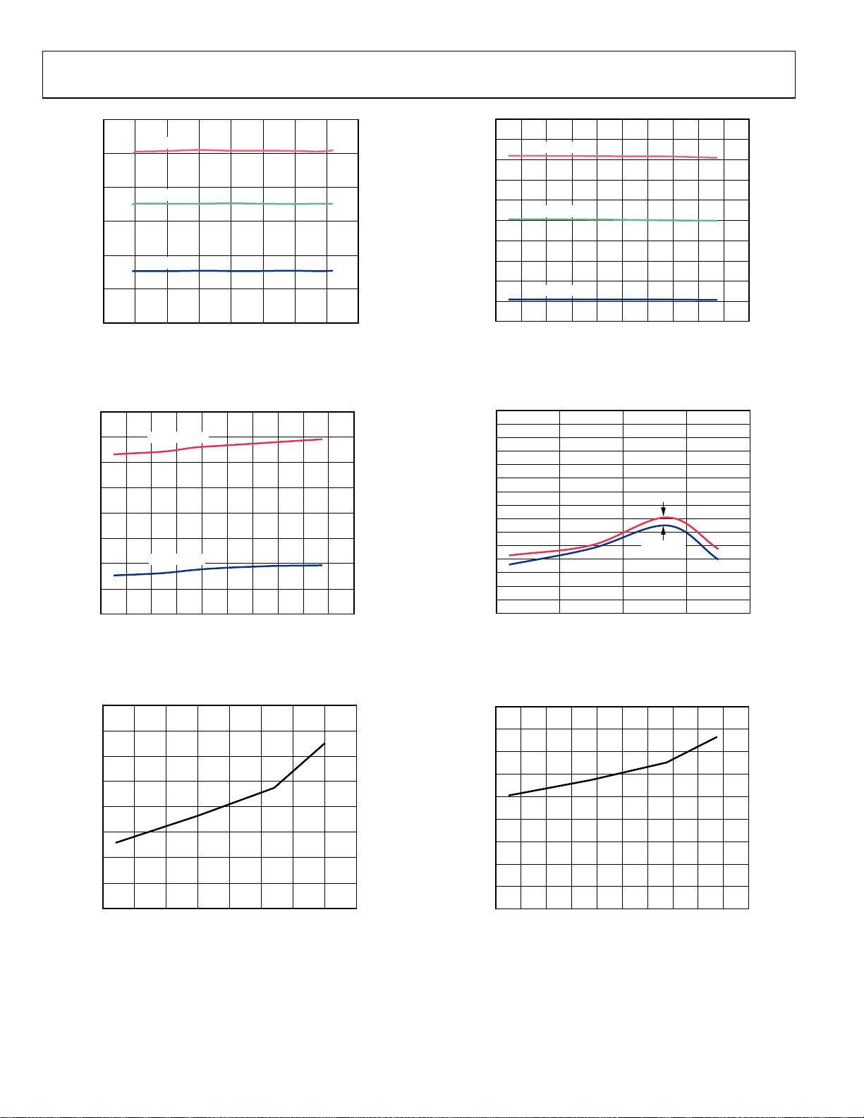
Figure 16. Shutdown Current vs. Temperature
Figure 17. UVLO Threshold vs. Temperature
Figure 19. Supply Current vs. Temperature
Figure 20. Enable Threshold vs. Temperature
Figure 18. Tracking Range
Figure 21. PGOOD Threshold vs. Temperature
Rev. 0 | Page 9 of 32
Page 10
ADP2441 Data Sheet
0
200
400
600
800
1000
1200
0 5 10 15 20 25 30 35 40
SWITCHING FREQUE NCY (kHz)
VIN (V)
f
SW
= 300kHz
f
SW
= 1MHz
f
SW
= 700kHz
10581-022
0
25
50
75
100
125
150
175
200
–50 –30 –10 10 30 50 70 90 110 130 150
ON TIMEAND OFF TIME (ns)
TEMPERATURE (°C)
MINIMUM ON
MINIMUM OFF
10581-024
100
120
140
160
180
200
220
240
260
–50 –25 0 25 50 75 100 125 150
HIGH-SI DE R
DS(ON)
(mΩ)
TEMPERATURE (°C)
10581-027
200
300
400
500
600
700
800
900
1000
1100
1200
–50 –30 –10 10 30 50 70 90 110 130 150
FREQUENCY (kHz)
TEMPERATURE (°C)
f
SW
= 300kHz
f
SW
= 1MHz
f
SW
= 700kHz
10581-023
1.50
1.52
1.54
1.56
1.58
1.60
1.62
1.64
1.66
1.68
1.70
1.72
1.74
1.76
1.78
1.80
–50 0 50 100 150
CURRENT (A)
TEMPERATURE (°C)
V
IN
= 36V
VIN = 4.5V
10581-126
0
20
40
60
80
100
120
140
160
180
–50 –30 –10 10 30 50 70 90 110 130 150
LOW-SIDE R
DS(ON)
(mΩ)
TEMPERATURE (°C)
10581-026
Figure 22. Switching Frequency vs. Supply
Figure 23. Minimum On Time and Minimum Off Time vs. Temperature
Figure 25. Switching Frequency vs. Temperature
Figure 26. Current Limit vs. Temperature
Figure 24. High-Side R
vs. Temperature
DS(ON)
Figure 27. Low-Side R
vs. Temperature
DS(ON)
Rev. 0 | Page 10 of 32
Page 11

Data Sheet ADP2441
10581-028
CH1 20.0mV
B
W
CH2 10.0V
CH4 200mA Ω
M4.00µs A CH4 120mA
1
4
2
T 41.40%
V
IN
= 24V
V
OUT
= 3.3V
F
SW
= 500kHz
V
OUT
INDUCTOR CURRENT
SW
10581-030
CH1 20.0mV
B
W
CH2 10.0V
CH4 500mA Ω
M1.00µs A CH2 9.80V
1
4
2
T 41.40%
V
OUT
INDUCTOR CURRENT
SW
V
IN
= 24V
V
OUT
= 3.3V
f
SW
= 500kHz
LOAD = 1A
10581-032
CH1 100mV
B
W
CH2 10V
CH4 500mA Ω
M200µs A CH4 690mA
1
4
2
T 79.80%
V
OUT
LOAD
SW
VIN = 24V
V
OUT
= 5V
f
SW
= 700kHz
LOAD STE P = 500mA
10581-029
CH1 20.0mV
B
W
CH2 10.0V
CH4 500mA Ω
M4.00µs A CH4 120mA
1
4
2
T 41.40%
V
IN
= 24V
V
OUT
= 3.3V
f
SW
= 500kHz
LOAD = 100mA
V
OUT
INDUCTOR CURRENT
SW
10581-031
CH1 200mV
B
W
CH2 10.0V
CH4 1.00A Ω
M2.00ms A CH1 60.0mV
1
4
2
T 49.40%
V
OUT
INDUCTOR CURRENT
SW
10581-033
CH1 50.0mV
B
W
CH2 10.0V
CH4 200mA Ω
M200µs A CH4 604mA
1
4
2
V
OUT
LOAD
SW
V
IN
= 24V
V
OUT
= 5V
f
SW
= 700kHz
LOAD STE P = 300mA
V
IN
V
= 24 V, V
IN
Figure 28. Pulse Skip Mode,
= 24 V, V
= 3.3 V, fSW = 500 kHz, No Load
OUT
Figure 29. PWM Mode,
= 3.3 V, fSW = 500 kHz, Load = 1 A
OUT
V
V
= 24 V, V
IN
= 24 V, V
IN
Figure 31. Pulse Skip Mode,
= 3.3 V, fSW = 500 kHz, Load = 100 mA
OUT
Figure 32. Hiccup Mode,
= 3.3 V, fSW = 500 kHz, Output Short to PGND
OUT
Figure 30. Load Transient Response,
V
= 24 V, V
IN
OUT
= 5 V, fSW = 700 kHz, Load Step = 500 mA
Rev. 0 | Page 11 of 32
V
= 24 V, V
IN
Figure 33. Load Transient Response,
= 5 V, fSW = 700 kHz, Load Step = 300 mA
OUT
Page 12

ADP2441 Data Sheet
10581-034
CH1 100mV
B
W
CH2 5.00V
CH4 500mA Ω
M200µs A CH4 690mA
1
4
2
V
OUT
LOAD
SW
VIN = 12V
V
OUT
= 5V
f
SW
= 300kHz
LOAD STE P = 500mA
10581-035
CH1 200mV
B
W
CH2 10.0V
CH4 500mA Ω
M200µs A CH4 550mA
1
4
2
V
OUT
LOAD
SW
VIN = 24V
V
OUT
= 12V
f
SW
= 300kHz
LOAD STE P = 500mA
10581-036
CH1 2.00V
B
W
CH4 2.00VCH3 2.00V
M1.00ms A CH3 1.64V
3
1
4
V
OUT
PGOOD
ENABLE
V
IN
= 24V
V
OUT
= 5V
f
SW
= 700kHz
10581-037
CH1 200mV
B
W
CH2 10.0V
CH4 500mA Ω
M200µs A CH4 600mA
1
4
2
V
OUT
LOAD
SW
V
IN
= 24V
V
OUT
= 12V
f
SW
= 600kHz
LOAD STE P = 500mA
10581-038
CH1 2.00V
B
W
CH4 2.00VCH3 5.00V
M 200µs A CH3 1.60V
3
1
4
V
OUT
PGOOD
ENABLE
VIN = 24V
V
OUT
= 5V
f
SW
= 700kHz
10581-039
CH1 2.00V
B
W
CH2 10.0V
B
W
CH3 10.0V
M4.00ms A CH3 5.00V
3
1
2
V
OUT
V
IN
SW
V
IN
= 36V
V
OUT
= 5V
f
SW
= 700kHz
V
= 12 V, V
IN
V
= 24 V, V
IN
Figure 34. Load Transient Response,
= 5 V, fSW = 300 kHz, Load Step = 500 mA
OUT
Figure 35. Load Transient Response,
= 12 V, fSW = 300 kHz, Load Step = 500 mA
OUT
V
= 24 V, V
IN
Figure 37. Load Transient Response,
= 12 V, fSW = 600 kHz, Load Step = 500 mA
OUT
Figure 38. Power-Good Shutdown,
V
= 24 V, V
IN
= 5 V, fSW = 700 kHz
OUT
Figure 36. Power Good Startup,
V
= 24 V, V
IN
= 5 V, fSW = 700 kHz
OUT
Figure 39. Startup with VIN,
V
= 36 V, V
IN
= 5 V, fSW = 700 kHz, No Load
OUT
Rev. 0 | Page 12 of 32
Page 13

Data Sheet ADP2441
10581-040
CH1 2.00V
B
W
CH2 10.0V
B
W
CH3 10.0V
M4.00ms A CH3 9.00V
3
1
2
V
OUT
V
IN
SW
V
IN
= 36V
V
OUT
= 5V
f
SW
= 700kHz
LOAD = 5Ω
10581-041
CH1 2.00V
B
W
CH2 10.0V
CH4 2.00VCH3 5.00V
M200µs A CH3 2.20V
3
1
2
4
V
OUT
ENABLE
SS
SW
V
IN
= 24V
V
OUT
= 5V
f
SW
= 700kHz
LOAD = 5Ω
10581-042
CH1 2.00V
B
W
CH2 10.0V
CH4 500mVCH3 5.00V
M2.00ms A CH3 2.20V
3
1
2
4
V
OUT
ENABLE
SS
SW
VIN = 24V
V
OUT
= 5V
f
SW
= 700kHz
LOAD = 5Ω
SS = 10nF
10581-143
CH1 2.00V
B
W
CH2 10.0V
CH4 2.00VCH3 5.00V
M1.00ms A CH3 1.40V
3
1
2
4
V
OUT
ENABLE
SS
SW
V
IN
= 24V
V
OUT
= 5V
f
SW
= 700kHz
–90
–50
–10
30
70
110
–70
–30
10
50
90
1 10 100
MAGNITUDE ( dB)
–200
–120
–40
40
120
200
–160
–80
0
80
160
PHASE (Degrees)
FREQUENCY (kHz)
CROSSOVE R = 58kHz : 1/12
f
SW
PHASE MARGI N = 55°
V
IN
= 24V
V
OUT
= 5V
f
SW
= 700kHz
LOAD = 1A
10581-144
V
= 36 V, V
IN
= 5 V, fSW = 700 kHz, Load = 5 Ω
OUT
Figure 41. Shutdown with Precision Enable,
V
Figure 40. Startup with VIN,
= 24 V, V
IN
= 5 V, fSW = 700 kHz, Load = 5 Ω
OUT
Figure 43. Soft Start Startup with Precision Enable,
V
= 24 V, V
IN
= 5 V, fSW = 700 kHz, No Load, Internal SS
OUT
Figure 44. Magnitude and Phase vs. Frequency
V
= 24 V, V
IN
Figure 42. Startup with Precision Enable,
= 5 V, fSW = 700 kHz, Load = 5 Ω, SS = 10 nF
OUT
Rev. 0 | Page 13 of 32
Page 14

ADP2441 Data Sheet
VIN
POWER STAGE
UVLO
INTERNAL LDO
VCC
BST
STATE MACHINE GATE
CONTROL LOGIC
EN
+
1.25V
FB
I
SS
+
+
–
V
REF
= 0.6V
SS/TRK
SW
PGND
NMOS
NMOS
SLOPE
COMPENSATION/
RAMP
GENERATOR
CURRENT-LIMIT
COMPARATOR
CURRENT SENSE
AMPLIFIER
REFERENCE
CURRENT
BAND GAP
REFERENCE
PWM
COMPARATOR
FREQ
OSC
HICCUP
TIMER
COMP
THRESHOLD
PULSE SKIP
ENABLE
CLOCK
ENABLE
V
CC
COMP
1V
PWM
HICCUP
+
+
–
AGND
115% OF
FEEDBACK
PGOOD
V
FB
86%OF
FEEDBACK
+
–
10581-043
INTERNAL BLOCK DIAGRAM
Figure 45. Block Diagram
Rev. 0 | Page 14 of 32
Page 15

Data Sheet ADP2441
COMPARATOR
S
R
REF
DRIVER
CLOCK
COMP
V
RAMP
V
FB
V
OUT
V
IN
PWM
I
L
R
SWL
× I
L
VC
SENSE_
OUT
Q
QB
RAMP
EMULATION
BLOCK
G
CS
g
m
10581-044
COMP
CONTROL
LOGIC
ADP2441
PULSE SKIP
THRESHOLD
1VDC
10581-045
THEORY OF OPERATION
The ADP2441 is a fixed frequency, current mode control, stepdown, synchronous switching regulator that is capable of
driving 1 A loads. The device operates with a wide input voltage
range from 4.5 V to 36 V, and its output is adjustable from 0.6 V
to 0.9 V × V
MOSFET and the low-side N-channel power MOSFET yield
high efficiency with medium to heavy loads. Pulse skip mode is
available to improve efficiency at light loads.
The ADP2441 includes programmable features, such as soft
start, output voltage, switching frequency, and power good.
These features are programmed externally via tiny resistors and
capacitors. The ADP2441 also includes protection features, such
as UVLO with hysteresis, output short-circuit protection, and
thermal shutdown.
CONTROL ARCHITECURE
The ADP2441 is based on the emulated peak current mode
control architecture.
Fixed Frequency Mode
A basic block diagram of the control architecture is shown in
Figure 46. With medium to heavy loads, the ADP2441 operates
in the fixed switching frequency PWM mode. The output
voltage, V
amplifier integrates the error between the feedback voltage and
the reference voltage (V
at the COMP pin. A current sense amplifier senses the valley
inductor current (I
power MOSFET is on and the high-side power MOSFET is off.
An internal oscillator initiates a PWM pulse to turn off the lowside power MOSFET and turn on the high-side power MOSFET
at a fixed switching frequency. When the high-side N-channel
power MOSFET is enabled, the valley inductor current
information is added to an emulated ramp signal, and then the
PWM comparator compares this value to the error voltage on
the COMP pin. The output of the PWM comparator modulates
the duty cycle by adjusting the trailing edge of the PWM pulse
that turns off the high-side power MOSFET and turns on the
low-side power MOSFET.
Slope compensation is programmed internally into the
emulated ramp signal and is automatically selected, depending
on the input voltage, output voltage, and switching frequency.
This prevents subharmonic oscillations for near or greater than
50% duty cycle operation. The one restriction of this feature is
that the inductor ripple current must be set between 0.2 A and
0.5 A to provide sufficient current information to the loop.
. The integrated high-side N-channel power
IN
, is sensed on the feedback pin, FB. An error
OUT
= 0.6 V) to generate an error voltage
REF
) during the off period when the low-side
L
Figure 46. Control Architecture Block Diagram
Pulse Skip Mode
The ADP2441 has built-in pulse skip circuitry that turns on
during light loads, switching only as necessary so that the
output voltage remains within regulation. This allows the
regulator to maintain high efficiency during operation with
light loads by reducing switching losses. The pulse skip circuitry
includes a comparator, which compares the COMP voltage to a
fixed pulse skip threshold.
Figure 47. Pulse Skip Comparator
With light loads, the output voltage discharges at a very slow
rate (load dependent). When the output voltage is within
regulation, the device enters sleep mode and draws a very small
quiescent current. As the output voltage drops below the
regulation voltage, the COMP voltage rises above the pulse skip
threshold. The device wakes up and starts switching until the
output voltage is within regulation.
As the load increases, the settling value of the COMP voltage
increases. At a particular load, COMP settles above the pulse skip
threshold, and the part enters the fixed frequency PWM mode.
Therefore, the load current at which COMP exceeds the pulse
skip threshold is defined as the pulse skip current threshold; the
value varies with the duty cycle and the inductor ripple current.
The measured value of pulse skip threshold over V
is given in
IN
Figure 13, Figure 14, and Figure 15.
Rev. 0 | Page 15 of 32
Page 16

ADP2441 Data Sheet
% OF V
OUT
SET
% OF V
OUT
SET
V
OUT
RISING
V
OUT
FALLING
110
90
116
84
POWER
GOOD
OVERVOLAGEUNDERVOLTAGE
PGOOD
UNDERVOLTAGE
POWER
GOOD
100
100
10581-047
10581-149
CH1 2.00V
B
W
CH2 1.00V
CH3 5.00V
M10.0ms A CH1 2.52V
3
1
2
V
OUT
ENABLE
SS
V
IN
= 24V
V
OUT
= 5V
f
SW
= 700kHz
LOAD = 1A
EXTERNAL S S = 10nF
MASTER
VOLTAGE
COMP
REF
SS/TRK
SW
FB
ADP2441
R
TRK_TOP
R
TRK_BOT
R
TOP
V
OUT
R
BOTTOM
10581-048
+
+
=
BOTTRK
TOPTRK
BOTTOM
TOP
MASTER
OUT
R
R
R
R
V
V
_
_
1
1
ADJUSTABLE FREQUENCY
The ADP2441 features a programmable oscillator frequency with
a resistor connected between the FREQ and AGND pins.
At power-up, the FREQ pin is forced to 1.2 V and current flows
from the FREQ pin to AGND; the current value is based on the
resistor value on the FREQ pin. Then, the same current is
replicated in the oscillator to set the switching frequency. Note
that the resistor connected to the FREQ pin should be placed as
close as possible to the FREQ pin (see the Applications
Information section for more information).
POWER GOOD
The PGOOD pin is an open-drain output that indicates the
status of the output voltage. When the voltage of the FB pin is
between 92% and 109% of the internal reference voltage, the
PGOOD output is pulled high, provided there is a pull-up
resistor connected to the pin. When the voltage of the FB pin is
not within this range, the PGOOD output is pulled low to
AGND. The PGOOD threshold is shown in Figure 48.
Likewise, the PGOOD pin is pulled low to AGND when the
input voltage is below the internal UVLO threshold, when the
EN pin is low, or when a thermal shutdown event has occurred.
establishing a voltage ramp slope at the SS pin, as shown in
Figure 49. The soft start period ends when the soft start ramp
voltage exceeds the internal reference of 0. 6 V. The ADP2441
also features an internal default soft start time of 2 ms. For more
information, see the Applications Information section.
Figure 49. External Soft Start
TRACKING
The ADP2441 has a tracking feature that allows the output
voltage to track an external voltage. This feature is especially
useful in a system where power supply sequencing and tracking
is required.
The ADP2441 SS/TRK pin is connected to the internal error
amplifier. The internal error amplifier includes three inputs: the
internal reference voltage, the SS/TRK voltage, and the feedback
voltage. The error amplifier regulates the feedback voltage to
the lower of the other two voltages. To track a master voltage,
tie the SS/TRK pin to a resistor divider from the master voltage
as shown in Figure 50.
Figure 48. PGOOD Threshold
In a typical application, a pull-up resistor connected between the
PGOOD pin and an external supply is used to generate a logic
signal. This pull-up resistor should range in value from 30 kΩ
to 100 kΩ, and the external supply should be less than 5.5 V.
SOFT START
The ADP2441 soft start feature allows the output voltage to ramp
up in a controlled manner, limiting the inrush current during
startup. An external capacitor connected between the SS/TRK
and AGND pins is required to program the soft start time.
The programmable soft start feature is useful when a load
requires a controlled voltage slew rate at startup. When the
regulator powers up and soft start is enabled, the internal
1 μA current source charges the external soft start capacitor,
Figure 50. Tracking Feature Block Diagram
The ratio of the slave output voltage to the master voltage is a
function of the two dividers as follows:
(1)
Rev. 0 | Page 16 of 32
Page 17

Data Sheet ADP2441
VOLTAGE (V)
TIME
MASTER VOLTAGE
SLAVE VOLTAGE
10581-049
VOLTAGE (V)
TIME
MASTER VOLTAGE
SLAVE VOLTAGE
10581-050
VIN
EN
FREQ AGND COMP
SW
ADP2441
R1
R2
V
OUT
V
IN
BST
FB
10581-051
Coincident Tracking
The most common mode of tracking is coincident tracking. In this
method, the slope of the slave voltage matches that of the master
voltage, as shown in Figure 51. As the master voltage rises, the
slave voltage rises identically. Eventually, the slave voltage reaches
its regulation voltage, at which point the internal reference takes
over the regulation while the SS/TRK input continues to increase,
thus preventing itself from influencing the output voltage.
itself to using a resistor divider from the VIN pin (or another
external supply) to program a desired UVLO threshold that is
higher than the fixed internal UVLO of 4.2 V. The hysteresis is
100 m V.
If a resistor divider is not used, a logic signal can be applied. A
logic high enables the part, and a logic low forces the part into
shutdown mode.
Figure 51. Coincident Tracking
For coincident tracking, select resistor values such that R
= R
TOP
and R
TRK_BOT
= R
in Equation 1.
BOTTOM
TRK_TOP
Ratiometric Tracking
In the ratiometric tracking scheme, the master and the slave
voltages rise with different slopes.
Figure 52. Ratiometric Tracking
For ratiometric tracking in which the master voltage rises faster
than the slave voltage (as shown in Figure 52), select R
R
TOP
and R
TRK_BOT
= R
in Equation 1.
BOTTOM
TRK_TOP
≥
UNDERVOLTAGE LOCKOUT (UVLO)
The UVLO function prevents the IC from turning on while the
input voltage is below the specified operating range to avoid an
undesired operating mode. If the input voltage drops below the
specified range, the UVLO function shuts off the device. The
rising input voltage threshold for the UVLO function is 4.2 V
with 200 mV hysteresis. The 200 mV of hysteresis prevents the
regulator from turning on and off repeatedly with slow voltage
ramp on the VIN pin.
PRECISION ENABLE/SHUTDOWN
The ADP2441 features a precision enable pin (EN) that can be used
to enable or shut down the device. The ±5% accuracy lends
Rev. 0 | Page 17 of 32
Figure 53. Precision Enable Used as a Programmable UVLO
CURRENT-LIMIT AND SHORT-CIRCUIT PROTECTION
The ADP2441 has a current-limit comparator that compares
the current sensed across the low-side power MOSFET to the
internally set reference current. If the sensed current exceeds
the reference current, the high-side power MOSFET is not
turned on in the next cycle and the low-side power MOSFET
stays on until the inductor current ramps down below the
current-limit level.
If the output is overloaded and the peak inductor current exceeds
the preset current limit for more than eight consecutive clock
cycles, the hiccup mode current-limit condition occurs. The
output goes to sleep for 6 ms, during which time the output is
discharged, the average power dissipation is reduced, and the
part wakes up with a soft start period. If the current-limit condition
is triggered again, the output goes to sleep and wakes up after 6 ms.
Figure 32 shows the current-limit hiccup mode when the output
is shorted to PGND.
THERMAL SHUTDOWN
If the ADP2441 junction temperature rises above 150°C, the
thermal shutdown circuit turns off the switching regulator. Extreme
junction temperatures can be the result of high current operation,
poor circuit board design, or high ambient temperature. A 25°C
hysteresis is included so that when a thermal shutdown occurs,
the ADP2441 does not return to normal operation until the
junction temperature drops below 125°C. Soft start is active
upon each restart cycle.
Page 18

ADP2441 Data Sheet
STRING
REF
BOTTOM
I
V
R =
−
×=
REF
REF
OUT
BOTTOMTOP
V
VV
RR
ADP2441
FB
R
TOP
R
FREQ
C
SS
V
OUT
R
BOTTOM
PGOOD
EXTERNAL
SUPPLY
FREQ SS/TRK
10581-052
Voltage (V)
R
(kΩ)
R
(kΩ)
0
10
20
30
40
50
60
70
80
90
100
0 200 400 600 800 1000 1200
DUTY CYCLE (%)
FREQUENCY (kHz)
D
MAX
D
MIN
10581-155
SW
FREQ
f
R
500,92
=
10581-053
200
300
400
500
600
700
800
900
1000
1100
1200
50 100 150 200 250 300 350
FREQUENCY (kHz)
RESISTANCE (kΩ)
APPLICATIONS INFORMATION
SELECTING THE OUTPUT VOLTAGE
The output voltage is set using a resistor divider connected between
the output voltage and the FB pin (see Figure 54). The resistor
divider divides down the output voltage to the 0.6 V FB regulation
voltage. The output voltage can be set to as low as 0.6 V and as
high as 90% of the power input voltage.
The ratio of the resistive voltage divider sets the output voltage,
and the absolute value of the resistors sets the divider string
current. For lower divider string currents, the small 50 nA
(0.1 μA maximum) FB bias current should be taken into
account when calculating the resistor values. The FB bias
current can be ignored for a higher divider string current;
however, using small feedback resistors degrades efficiency at
very light loads.
To limit degradation of the output voltage accuracy due to FB
bias current to less than 0.005% (0.5% maximum), ensure that
the divider string current is greater than 20 μA. To calculate the
desired resistor values, first determine the value of the bottom
resistor, R
where:
V
is the internal reference and equals 0.6 V.
REF
I
is the resistor divider string current.
STRING
Then calculate the value of the top resistor, R
BOTTOM
, as follows:
(2)
, as follows:
TOP
(3)
due to the requirement of minimum on time and minimum off
time for current sensing and robust operation. However, the
choice is also influenced by whether there is a need for small
external components. For example, for small, area limited
power solutions, higher switching frequencies are required.
Figure 55. Duty Cycle vs. Switching Frequency
Calculate the value of the frequency resistor using the following
equation:
(4)
where R
is in kΩ, and fSW is in kHz.
FREQ
Table 6 and Figure 56 provide examples of frequency resistor
values, which are based on the switching frequency.
Table 6. Frequency Resistor Selection
R
(kΩ) Frequency
FREQ
308 300 kHz
132 700 kHz
92.5 1 MHz
Figure 54. Voltage Divider
Table 5. Output Voltage Selection
TOP
12 190 10
5 73 10
3.3 45 10
1.2 10 10
SETTING THE SWITCHING FREQUENCY
The choice of the switching frequency depends on the required
dc-to-dc conversion ratio and is limited by the minimum and
maximum controllable duty cycle, as shown in Figure 55. This is
BOTTOM
Figure 56. Frequency vs. Resistance
Rev. 0 | Page 18 of 32
Page 19

Data Sheet ADP2441
SS
SS
SS
REF
C
I
t
V
=
SWESR
OUT
PP
OUT
MININ
fRDIV
DDI
C
)(
)1(
_
××−
−××
=
−××
−×
−××
−××
SW
IN
−××
SOFT START
The soft start function limits the input inrush current and
prevents output overshoot at startup. The soft start time is
programmed by connecting a small ceramic capacitor between
the SS/TRK and AGND pins, with the value of this capacitor
defining the soft start time, t
, as follows:
SS
(5)
where:
V
is the internal reference voltage and equals 0.6 V.
REF
I
is the soft start current and equals 1 μA.
SS
C
is the soft start capacitor value.
SS
Table 7. Soft Start Time Selection
Soft Start Capacitor (nF) Soft Start Time (ms)
5 3
10 6
20 12
Alternatively, the user can float the SS/TRK pin and use the
internal soft start time of 2 ms.
EXTERNAL COMPONENTS SELECTION
Input Capacitor Selection
The input current to a buck regulator is pulsating in nature. The
current is zero when the high-side switch is off and is approximately equal to the load current when the switch is on. Because
switching occurs at reasonably high frequencies (300 kHz to
1 MHz), the input bypass capacitor usually supplies most of
the high frequency current (ripple current), allowing the input
power source to supply only the average (dc) current. The input
capacitor needs a sufficient ripple current rating to handle the
input ripple and needs an ESR that is low enough to mitigate the
input voltage ripple. In many cases, different types of capacitors
are placed in parallel to minimize the effective ESR and ESL.
The minimum input capacitance required for a particular load is
(6)
where:
V
is the desired input ripple voltage.
PP
R
is the equivalent series resistance of the capacitor.
ESR
I
is the maximum load current.
OUT
It is recommended to use a ceramic bypass capacitor because
the ESR associated with this type of capacitor is near zero,
simplifying the equation to
DDI
C
_
OUT
=
MININ
×
PP
In addition, it is recommended to use a ceramic capacitor with a
voltage rating that is 1.5 times the input voltage with X5R and X7R
dielectrics. Using Y5V and Z5U dielectrics is not recommended
)1(
fV
(7)
SW
Rev. 0 | Page 19 of 32
due to their poor temperature and dc bias characteristics. Table 10
shows a list of recommended MLCC capacitors from Murata
and Taiyo Yuden.
For large step load transients, add more bulk capacitance by, for
example, using electrolytic or polymer capacitors. Make sure
that the ripple current rating of the bulk capacitor exceeds the
minimum input ripple current of a particular design.
Inductor Selection
The high switching frequency of the ADP2441 allows for
minimal output voltage ripple even when small inductors are used.
Selecting the size of the inductor involves considering the trade-off
between efficiency and transient response. A smaller inductor
results in larger inductor current ripple, which provides excellent
transient response but degrades efficiency. Due to the high
switching frequency of the ADP2441, using shielded ferrite core
inductors is recommended because of their low core losses and
low EMI.
The inductor ripple current also affects the stability of the loop
because the ADP2441 uses the emulated peak current mode
architecture. In the traditional approach of slope compensation,
the user sets the inductor ripple current and then sets the slope
compensation using an external ramp resistor. In most cases, the
inductor ripple current is typically set to be 1/3 of the maximum
load current for optimal transient response and efficiency. The
ADP2441 has internal slope compensation, which assumes that
the inductor ripple current is set to 0.3 A (30% of the maximum
load of 1 A), eliminating the need for an external ramp resistor.
For the ADP2441, choose an inductor such that the peak-topeak ripple current of the inductor is between 0.2 A and 0.5 A
for stable operation.
Therefore, calculate the inductor value as follows:
)(
VVV
IN
OUT
SW
OUT
(8)
LfV
××
)(5)(2
VVV
OUT
L
IN
fV
×
OUT
VVV
≤≤
OUT
IN
)(3.3
(9)
VVV
IN
OUT
fV
×
SW
=∆
I
L
0.2 A ≤ ΔI
OUT
=
L
IDEAL
OUT
IN
≤ 0.5 A
L
×
IN
IN
fV
SW
where:
V
is the input voltage.
IN
V
is the desired output voltage.
OUT
f
is the regulator switching frequency.
SW
For applications with a wide input (V
) range, choose the
IN
inductor based on the geometric mean of the input voltage
extremes.
VVV
×=
MAXIN
GEOMETRICIN
)(
_
MININ
_
where:
V
is the maximum input voltage.
IN_MAX
V
is the minimum input voltage.
IN_MIN
Page 20

ADP2441 Data Sheet
SW
GEOMETRICIN
OUT
GEOMETRICIN
OUT
IDEAL
fV
VVV
L
×
−××
=
)(
)(
)(3.3
300
24 5 39
47
2
)(
_
L
MAXLOAD
PEAKL
III∆
+=
××
+×∆≅∆
)(
8
1
MINOUT
SW
LRIPPLE
Cf
ESRIV
)(8
)(
ESRIVf
I
C
LRIPPLE
SW
L
MINOUT
×∆−∆××
∆
≅
∆×
×∆≅
DROOPSW
STEPOUTMINOUT
Vf
IC
3
)()(
The inductor value is based on V
IN(GEOMETRIC)
Table 8. Inductor Values for Various V
Combinations
Inductor Value
fSW (kHz) VIN (V) V
(V) Min (µH) Max (µH)
OUT
300 12 3.3 22 27
300 12 5 27 33
300 24 3.3 27 33
300 24 12 56 68
300 36 3.3 27 33
300 36 5 39 47
300 36 12 68 82
600 12 3.3 12 15
600 12 5 15 18
600 24 3.3 15 18
600 24 5 18 22
600 24 12 27 33
600 36 3.3 15 18
600 36 5 22 27
1000 12 5 6.8 10
1000 24 5 10 12
1000 24 12 18 22
1000 36 5 12 15
To avoid inductor saturation and ensure proper operation, choose
the inductor value so that neither the saturation current nor
the maximum temperature rated current ratings are exceeded.
Inductor manufacturers specify both of these ratings in data
sheets, or the rating can be calculated as follows:
(10)
where:
I
ΔI
is the maximum dc load current.
LOAD(MAX )
is the peak-to-peak inductor ripple current.
L
Table 9. Recommended Inductors
Small Size Inductors
Value (µH)
(<10 mm × 10 mm)
10 XAL4040-103ME MSS1260
18 LPS6235-183ML MSS1260
33 LPS6235-33ML MSS1260
15 XAL4040-153ME MSS1260
as follows:
, V
, and fSW
IN
OUT
Large Size Inductors
(>10 mm × 10 mm)
Output Capacitor Selection
The output capacitor selection affects both the output voltage
ripple and the loop dynamics of the regulator. The ADP2441 is
designed to operate with small ceramic output capacitors that
have low ESR and ESL; therefore, the device can easily meet
tight output voltage ripple specifications. For best performance,
use X5R or X7R dielectric capacitors with a voltage rating that is
1.5 times the output voltage and avoid using Y5V and Z5U
dielectric capacitors, which have poor temperature and dc bias
characteristics. Table 10 lists some recommended capacitor
from Murata and Taiyo Yuden.
For acceptable maximum output voltage ripple, determine the
minimum output capacitance, C
OUT(MIN)
, as follows:
(11)
Therefore,
(12)
where:
ΔV
is the allowable peak-to-peak output voltage ripple.
RIPPLE
ΔI
is the inductor ripple current.
L
ESR is the equivalent series resistance of the capacitor.
f
is the switching frequency of the regulator.
SW
If there is a step load requirement, choose the output capacitor
value based on the value of the step load. For the maximum acceptable output voltage droop/overshoot caused by the step load,
(13)
where:
ΔI
f
SW
ΔV
is the load step.
OUT(STEP)
is the switching frequency of the regulator.
is the maximum allowable output voltage droop/overshoot.
DROOP
Select the largest output capacitance given by Equation 12 and
Equation 13. When choosing the type of ceramic capacitor for the
output filter of the regulator, select one with a nominal capacitance
that is 20% to 30% larger than the calculated value because the
effective capacitance degrades with dc voltage and temperature.
Figure 57 shows the capacitance loss due to the output voltage
dc bias for three X7R MLCC capacitors from Murata.
Rev. 0 | Page 20 of 32
Page 21

Data Sheet ADP2441
0
30.0
24.6
19.2
13.8
8.40
3.00
5 10
DC BIAS VOLTAGE (V)
CAPACITANCE (µF)
15 20 25
22µF/25V
10µF/25V
10581-157
4.7 µF/50 V
GRM31CR71H475KA12L
UMK325B7475MMT
ADP2441
VFB
g
m
COMP
AGND
R
COMP
C
COMP
0.6V
10581-054
PULSE-WIDTH
MODULATOR
Gm
V
REF
= 0.6V
INDUCTOR
CURRENT
SENSE
V
OUT
V
IN
V
COMP
C
COMP
C
OUT
R
COMP
R
LOAD
ADP2441
I
L
g
m
10581-055
LOOP COMPENSATION
The ADP2441 uses peak current mode control architecture for
excellent load and line transient response. This control architecture
has two loops: an external voltage loop and an inner current loop.
The inner current loop senses the current in the low-side switch
and controls the duty cycle to maintain the average inductor
current. Slope compensation is added to the inner current loop
to ensure stable operation when the duty cycle is above 50%.
The external voltage loop senses the output voltage and adjusts
the duty cycle to regulate the output voltage to the desired
value. A transconductance amplifier with an external series RC
network connected to the COMP pin compensates the external
Figure 57. Capacitance vs. DC Bias Voltage
For example, to attain 20 μF of output capacitance with an output
voltage of 5 V while providing some margin for temperature
variation, use a 22 μF capacitor with a voltage rating of 25 V
and a 10 μF capacitor with a voltage rating of 25 V in parallel.
This configuration ensures that the output capacitance is
sufficient under all conditions and, therefore, that the device
exhibits stable behavior.
voltage loop.
Table 10. Recommended Output Capacitors for ADP2441
Vendor
Capacitor Murata Taiyo Yuden
10 µF/25 V GRM32DR71E106KA12L TMK325B7106KN-TR
22 µF/25 V GRM32ER71E226KE15L TMK325B7226MM-TR
47 µF/6.3 V GCM32ER70J476KE19L JMK325B7476MM-TR
BOOST CAPACITOR
The boost pin (BST) is used to power up the internal driver for the
high-side power MOSFET. In the ADP2441, the high-side power
MOSFET is an N-channel device to achieve high efficiency in
mid and high duty cycle applications. To power up the high-side
driver, a capacitor is required between the BST and SW pins.
The size of this boost capacitor is critical because it affects the
light load functionality and efficiency of the device. Therefore,
it is strongly recommended to use a 10 nF ceramic boost capacitor
with a voltage rating of 50 V between the BST and SW pins and
to place the capacitor as close as possible to the IC.
VCC CAPACITOR
The ADP2441 has an internal regulator to power up the internal
controller and the low-side driver. The VCC pin is the output of
the internal regulator. The internal regulator provides the pulse
current when the low-side driver turns on. Therefore, it is recommended that a 1 µF ceramic capacitor be placed between the VCC
and PGND pins as close as possible to the IC and that a 1 µF
ceramic capacitor be placed between the VCC and AGND pins.
Figure 58. RC Compensation Network
LARGE SIGNAL ANALYSIS OF THE LOOP COMPENSATION
The control loop can be broken down into the following three
sections:
• V
• V
• I
Rev. 0 | Page 21 of 32
OUT
COMP
to V
L
to V
to IL
OUT
COMP
Figure 59. Large Signal Model
Page 22

ADP2441 Data Sheet
)(
)(
)(
sZg
V
V
sV
sV
COMP
m
OUT
REF
OUT
COMP
××=
CS
COMP
L
G
sV
sI
=
)(
)(
)(
)(
)(
sZ
sI
sV
FILT
L
OUT
=
COMP
COMPCOMP
COMP
Cs
CRs
sZ
×
××+=1
)(
OUT
LOAD
LOAD
FILT
CRs
R
sZ
××+=1
)(
)()()( sZsZ
V
V
GgsH
FILT
COMP
OUT
REF
CS
m
××××=
REF
OUT
CS
m
OUT
CROSSOVER
CROSSOVERCOMP
V
V
Gg
Cf
fZ ×
×
×××
=
π
2
)(
CRf
×××π×+
21
82
1
CROSSOVER
COMP
ZERO
f
CR
f
COMP
≈
××π×
=
REF
OUTOUT
CS
m
CROSSOVER
COMP
V
VC
Gg
f
R
×
×
×
×π××=2
9.0
COMP
ZERO
COMP
RfC××π×=2
1
Correspondingly, there are three transfer functions:
(14)
(15)
(16)
where:
g
is the transconductance of the error amplifier and equals
m
250 µA / V.
G
is the current sense gain and equals 2 A/ V.
CS
V
is the output voltage of the regulator.
OUT
V
is the internal reference voltage and equals 0.6 V.
REF
Z
(s) is the impedance of the RC compensation network that
COMP
forms a pole at the origin and a zero as expressed in Equation 17.
At the crossover frequency, the gain of the open-loop transfer
function is unity.
H(f
CROSSOVER
) = 1 (20)
This yields Equation 21 for the RC compensation network
impedance at the crossover frequency.
(21)
Placing s = f
fZ
CROSSOVERCOMP
CROSSOVER
in Equation 17,
=
)(
2
CROSSOVER
CROSSOVER
COMPCOMP
COMP
Cf
××π×
(22)
To ensure that there is sufficient phase margin at the crossover
frequency, place the compensator zero at 1/8 of the crossover
frequency, as shown in the following equation:
(23)
(17)
(s) is the impedance of the output filter and is expressed as
Z
FI LT
(18)
where s is the angular frequency, which can be written as s = 2πf.
The overall loop gain, H(s), is obtained by multiplying the three
transfer functions previously mentioned as follows:
(19)
When the switching frequency (f
), output voltage (V
SW
output inductor (L), and output capacitor (C
) values are
OUT
OUT
),
selected, the unity crossover frequency can be set to 1/12 of the
switching frequency.
Solving Equation 21, Equation 22, and Equation 23 yields the
value for the resistor and capacitor in the RC compensation
network, as shown in Equation 24 and Equation 25.
(24)
(25)
Using these equations allows calculating the compensations for
the voltage loop.
Rev. 0 | Page 22 of 32
Page 23

Data Sheet ADP2441
kΩ10
μA60
6.0
===
STRING
REF
BOTTOM
I
V
R
−
×=
REF
REF
OUT
BOTTOMTOP
V
VV
RR
SW
FREQ
f
R
500,92
=
SS
SS
SS
REF
C
I
t
V
=
REF
SSSS
SS
V
tIC×
=
nF10
V6.0
ms6μA1=×
=
SS
C
SW
IN
OUT
IN
OUT
IDEAL
fV
VVV
L
×
−××
=
)(3.3
μH3.18μH66.18
kHz700V24
V)524(V53.3
≈=
×
−××
=
IDEAL
L
SW
PP
OUT
MININ
fV
DDI
C
×
−××
=
)1(
_
μF9.4
kHz700V05.0
)22.01(22.0A1
_
≈
×
−××
=
MININ
C
DESIGN EXAMPLE
Consider an application with the following specifications:
• V
• V
=24 V ± 10%
IN
= 5 V ± 1%
OUT
• Switching frequency = 700 kHz
• Load = 800 mA typical
• Maximum load current = 1 A
• Soft start time = 6 ms
• Overshoot ≤ 2% under all load transient conditions
Soft Start Capacitor
For a given soft start time, the soft start capacitor can be calculated
using Equation 5,
CONFIGURATION AND COMPONENTS SELECTION
Resistor Divider
The first step in selecting the external components is to
calculate the resistance of the resistor divider that sets the
output voltage.
Using Equation 2 and Equation 3,
×=
R
TOP
kΩ10 =
Switching Frequency
Choosing the switching frequency involves considering the
trade-off between efficiency and component size. Low
frequency improves the efficiency by reducing the gate losses
but requires a large inductor. The choice of high frequency is
limited by the minimum and maximum duty cycle.
Table 11. Duty Cycle
VIN Duty Cycle
24 V (Nominal) D
26 V (10% Above Nominal) D
22 V (10% Less than Nominal) D
Based on the estimated duty cycle range, choose the switching
frequency according to the minimum and maximum duty cycle
limitations, as shown in Figure 55. For example, a 700 kHz,
frequency is well within the maximum and minimum duty
cycle limitations.
Using Equation 4,
−
V6.0V5
V6.0
kΩ3.73
NOMINAL
= 19%
MIN
= 23%
MAX
= 20.8%
Inductor Selection
Select the inductor by using Equation 9.
In Equation 9, V
= 24 V, V
IN
OUT
= 5 V, I
LOAD (MAX)
= 1 A, and fSW =
700 kHz, which results in L = 18.66 µH. When L = 18 μH (the
closest standard value) in Equation 8, ΔI
= 0.314 A. Although
L
the maximum output current required is 1 A, the maximum
peak current is 1.6 A. Therefore, the inductor should be rated
for higher than 1.6 A current.
Input Capacitor Selection
The input filter consists of a small 0.1 µF ceramic capacitor
placed as close as possible to the IC.
The minimum input capacitance required for a particular load is
where:
= 50 mV.
V
PP
I
= 1 A.
OUT
D = 0.23.
f
= 700 kHz.
SW
Therefore,
Choosing an input capacitor of 10 µF with a voltage rating of
50 V ensures sufficient capacitance over voltage and temperature.
= 132 kΩ
R
FREQ
Rev. 0 | Page 23 of 32
Page 24

ADP2441 Data Sheet
)(8
)(
ESRIVf
I
C
LRIPPLE
SW
L
MINOUT
×∆−∆××
∆
≅
∆×
∆≅
DROOPSW
STEPOUTMINOUT
Vf
IC
3
)()(
F22
V1.0kHz700
3
5.0
)(
µ≈
×
×≅
MINOUT
C
×
×π×
COMP
ZERO
COMP
RfC××π×=2
1
×
×π×
6.0
522
2250
3.582
pF180pF185
1183.72
1
≈=
×××
=
π
COMP
C
Output Capacitor Selection
Select the output capacitor by using Equation 12 and Equation 13:
Equation 12 is based on the output voltage ripple (ΔV
RIPPLE
),
which is 1% of the output voltage.
Equation 13 calculates the capacitor selection based on the
transient load performance requirement of 2%. Perform these
calculations, and then use the equation that yields the larger
capacitor size to select a capacitor.
In this example, the values listed in Tab l e 12 are substituted for
the variables in Equation 12 and Equation 13.
Selecting the crossover frequency to be 1/12 of the switching
frequency and placing the zero frequency at 1/8 of the crossover
frequency ensures that there is enough phase margin in the system.
Table 13. Calculated Parameter Value
Parameter Test Conditions/Comments Value
f
f
V
gm Transconductance of error
1/12 of f
CROSSOVER
1/8 of f
ZERO
Fixed reference 0.6 V
REF
58.3 kHz
SW
7.3 kHz
CROSSOVER
250 µA/V
amplifier
GCS Current sense gain 2 A/V
C
Output capacitor 22 µF
OUT
V
Output voltage 5 V
OUT
Based on the values listed in Table 13, calculate the compensation value:
Table 12. Requirements
Parameter Test Conditions/Comments Value
Ripple Current Fixed at 0.3 A for the ADP2441 0.3 A
Voltage Ripple 1% of V
Voltage Droop Due
2% of V
50 mV
OUT
100 mV
OUT
to Load Transient
ESR 5 mΩ
fSW 700 kHz
The calculation based on the output voltage ripple (see
Equation 12) dictates that the minimum output capacitance is
C
≅
)(
MINOUT
A3.0
×−××
μF1.1
=
)mΩ5A3.0mV50(kHz7008
whereas the calculation based on the transient load (see
Equation 13) dictates that the minimum output capacitance is
To meet both requirements, use the value determined by the
latter equation. As shown in Figure 57, capacitance degrades
with dc bias; therefore, choose a capacitor that is 1.5 times the
calculated value.
C
= 1.5 × 22 µF = 32 µF
OUT
Compensation Selection
Calculate the compensation component values for the feedback
loop by using the following equations:
R
COMP
f
×=29.0
CROSSOVER
Gg
×
m
×
CS
VC
OUTOUT
V
REF
R
COMP
×= k121
9.0
×
×
Ω≈
The closest standard resistor value is 118 kΩ. Therefore,
SYSTEM CONFIGURATION
Configure the system as follows:
1. Connect a capacitor of 1 µF between the VCC and PGND
pins and another capacitor of 1 µF between the VCC and
AGND pins. For best performance, use ceramic X5R or
X7R capacitors with a 25 V voltage rating.
2. Connect a ceramic capacitor of 10 nF with a 50 V voltage
rating between the BST and SW pins.
3. Connect a resistor between the FREQ and AGND pins as
close as possible to the IC.
4. If using the power-good feature, connect a pull-up resistor
of 50 kΩ to an external supply of 5 V.
5. Connect a capacitor of 10 nF between the SS and AGND pins.
If the tracking feature is needed, connect a resistor divider
between the TRK pin and another supply, as shown in
Figure 50.
See Figure 60 for a schematic of this design example and Tabl e 14
for the calculated component values.
Rev. 0 | Page 24 of 32
Page 25

Data Sheet ADP2441
V
IN
24V
FB
COMP
EN
PGOOD
FREQ
SS/TRK
PGND
VIN
SW
BST
AGND
VCC
ADP2441
V
OUT
5V, 1A
C3
1µF/25V
C4
1µF/25V
C11
10nF
L1
18µH
R9
132kΩ
R7
50kΩ
EXT
PGOOD
TRK
R5
118kΩ
C6
0.1µFC722µF
C2
4.7µF/
50V
C1
4.7µF/
50V
C5
10nF/50V
C10
180pF
R3
10kΩ
C8
10µF
10581-057
R2
73.3kΩ
1
R2
74 kΩ
Resistor, 1/10 W, 1%, 0603, SMD
TYPICAL APPLICATION CIRCUITS
DESIGN EXAMPLE
VIN = 24 V ± 10%, V
= 5 V, fSW = 700 kHz.
OUT
Figure 60. ADP2441 Typical Application Circuit, V
= 24 V ± 10%, V
IN
= 5 V, fSW = 700 kHz
OUT
Table 14. Calculated Component Values for Figure 60
Qt y. Ref Value Description Part Number
2 C1, C2 4.7 µF Capacitor ceramic, X7R, 50 V GRM31CR71H475KA12L
2 C3, C4 1 µF Capacitor ceramic, 1 µF, 25 V, X7R, 10%, 0603 GRM188R71E105KA12D
2 C5, C11 10 nF Capacitor ceramic, 10,000 pF, 50 V, 10%, X7R, 603 ECJ-1VB1H103K
1 C7 22 µF Capacitor ceramic, 22 µF, 25 V, X7R, 1210 GRM32ER71E226K
1 C8 10 µF Capacitor ceramic, 10 µF, 25 V, X7R, 1210 GRM32DR71E106KA12L
1 L1 18.3 µH Inductor, 18.3 µH CoilCraft MSS1260T-183NLB
1 C6 0.1 µF Capacitor ceramic, 0.1 µF, 50 V, X7R, 0805 ECJ-2FB1H104K
1 C10 185 pF Capacitor ceramic, 50 V Vishay, Panasonic
1 R9 132 kΩ Resistor, 1/10 W, 1%, 0603, SMD
1 R5 118 kΩ Resistor, 1/10 W, 1%, 0603, SMD
1 R3 10 kΩ Resistor, 1/10 W, 1%, 0603, SMD
1 R7 50 kΩ Resistor, 1/10 W, 1%, 0603, SMD
Rev. 0 | Page 25 of 32
Page 26

ADP2441 Data Sheet
R7
50kΩ
EXT
V
IN
24V
F
SW
600kHz
FB
COMP
EN
PGOOD
FREQ
SS/TRK
PGND
VIN
SW
BST
AGND
VCC
ADP2441
V
OUT
12V, 1A
C3
1µF/25V
C4
1µF/25V
C11
10nF
L1
33.3µH
R9
154kΩ
PGOOD
TRK
R5
121kΩ
C6
0.1µFC722µF/
25V
C2
4.7µF/
50V
C1
4.7µF/
50V
C5
10nF/50V
C10
220pF
R3
10kΩ
10581-058
R2
191kΩ
1
R7
50 kΩ
Resistor, 1/10 W, 1%, 0603, SMD
OTHER TYPICAL CIRCUIT CONFIGURATIONS
VIN = 24 V ± 10%, V
= 12 V, fSW = 600 kHz.
OUT
Figure 61. ADP2441 Typical Application Circuit, V
= 24 V ± 10%, V
IN
= 12 V, fSW = 600 kHz
OUT
Table 15. Calculated Component Values for Figure 61
Qt y. Ref Value Description Part Number
2 C1, C2 4.7 µF Capacitor ceramic, X7R, 50 V GRM31CR71H475KA12L
2 C3, C4 1 µF Capacitor ceramic, 1 µF, 25 V, X7R, 10%, 0603 GRM188R71E105KA12D
2 C5, C11 10 nF Capacitor ceramic, 10000 pF, 50 V, 10%, X7R, 0603 ECJ-1VB1H103K
1 C7 22 µF Capacitor ceramic, 22 µF, 25 V, X7R, 1210 GRM32ER71E226K
1 L1 33.3 µH Inductor, 33.3 µH CoilCraft MSS1038-333ML
1 C6 0.1 µF Capacitor ceramic, 0.1 µF, 50 V, X7R, 0805 ECJ-2FB1H104K
1 C10 220 pF Capacitor ceramic, 50 V Vishay, Panasonic
1 R9 154 kΩ Resistor, 1/10 W, 1%, 0603, SMD
1 R5 121 kΩ Resistor, 1/10 W, 1%, 0603, SMD
1 R2 191 kΩ Resistor, 1/10 W, 1%, 0603, SMD
1 R3 10 kΩ Resistor, 1/10 W, 1%, 0603, SMD
Rev. 0 | Page 26 of 32
Page 27

Data Sheet ADP2441
R7
50kΩ
EXT
V
IN
12V
F
SW
500kHz
FB
COMP
EN
PGOOD
FREQ
SS/TRK
PGND
VIN
SW
BST
AGND
VCC
ADP2441
V
OUT
5V, 1A
C3
1µF/25V
C4
1µF/25V
C11
10nF
L1
18µH
R9
185kΩ
PGOOD
TRK
R5
118kΩ
C6
0.1µF
C7
22µF
C8
22µF
C2
4.7µF/
50V
C1
4.7µF/
50V
C5
10nF/50V
C10
270pF
R3
10kΩ
10581-059
R2
73.3kΩ
1
R5
118 kΩ
Resistor, 1/10 W, 1%, 0603, SMD
VIN = 12 V ± 10%, V
= 5 V, fSW = 500 kHz.
OUT
Figure 62. ADP2441 Typical Application Circuit, V
= 12 V ± 10%, V
IN
= 5 V, fSW = 500 kHz
OUT
Table 16. Calculated Component Values for Figure 62
Qt y. Ref Value Description Part Number
2 C1, C2 4.7 µF Capacitor ceramic, X7R, 50 V GRM31CR71H475KA12L
2 C3, C4 1 µF Capacitor ceramic, 1 µF, 25 V, X7R, 10%, 0603 GRM188R71E105KA12D
2 C5, C11 10 nF Capacitor ceramic, 10,000 pF, 50 V, 10%, X7R, 0603 ECJ-1VB1H103K
1 C7 22 µF Capacitor ceramic, 22 µF, 25 V, X7R, 1210 GRM32ER71E226K
1 C8 22 µF Capacitor ceramic, 22 µF, 25 V, X7R, 1210
1 L1 18.3 µH Inductor, 18.3 µH CoilCraft MSS1038-183ML
1 C6 0.1 µF Capacitor ceramic, 0.1 µF, 50 V, X7R, 0805 ECJ-2FB1H104K
1 C10 270 pF Capacitor ceramic, 50 V Vishay, Panasonic
1 R9 185 kΩ Resi stor, 1/10 W, 1%, 0603, SMD
1 R2 74 kΩ Resistor, 1/10 W, 1%, 0603, SMD
1 R3 10 kΩ Resistor, 1/10 W, 1%, 0603, SMD
1 R7 50 kΩ Resistor, 1/10 W, 1%, 0603, SMD
Rev. 0 | Page 27 of 32
Page 28

ADP2441 Data Sheet
R7
50kΩ
EXT
V
IN
36V
F
SW
300kHz
FB
COMP
EN
PGOOD
FREQ
SS/TRK
PGND
VIN
SW
BST
AGND
VCC
ADP2441
V
OUT
3.3V, 1A
C3
1µF/25V
C4
1µF/25V
C11
10nF
L1
33.3µH
R9
300kΩ
PGOOD
TRK
R5
91kΩ
C6
0.1µF
C7
47µFC847µF
C2
4.7µF/
50V
C1
4.7µF/
50V
C5
10nF/50V
C10
560pF
R3
10kΩ
10581-060
R2
45kΩ
VIN = 36 V ± 10%, V
= 3.3 V, fSW = 300 kHz.
OUT
Figure 63. ADP2441 Typical Application Circuit, V
= 36 V ± 10%, V
IN
= 3.3 V, fSW = 300 kHz
OUT
Table 17. Calculated Component Values for Figure 63
Qt y. Ref Value Description Part Number
2 C1, C2 4.7 µF Capacitor ceramic, X7R, 50 V GRM31CR71H475KA12L
2 C3, C4 1 µF Capacitor ceramic, 1 µF, 25 V, X7R, 10%, 0603 GRM188R71E105KA12D
2 C5, C11 10 nF Capacitor ceramic, 10,000 pF, 50 V, 10%, X7R, 0603 ECJ-1VB1H103K
1 C7 47 µF Capacitor ceramic, 47 µF, 6.3 V, X7R, 1210 GRM32ER70J476KE20L
1 C8 47 µF Capacitor ceramic, 47 µF, 6.3 V, X7R, 1210 GRM32ER70J476KE20L
1 L1 33.3 µH Inductor, 33.3 µH CoilCraft MSS1038T-333ML
1 C6 0.1 µF Capacitor ceramic, 0.1 µF, 50 V, X7R, 0805 ECJ-2FB1H104K
1 C10 560 pF Capacitor ceramic, 50 V Vishay, Panasonic
1 R9 300 kΩ Resistor, 1/10 W, 1%, 0603, SMD
1 R5 91 kΩ Resistor, 1/10 W, 1%, 0603, SMD
1 R2 45 kΩ Resistor, 1/10 W, 1%, 0603, SMD
1 R3 10 kΩ Resistor, 1/10 W, 1%, 0603, SMD
1 R7 50 kΩ Resistor, 1/10 W, 1%, 0603, SMD
Rev. 0 | Page 28 of 32
Page 29

Data Sheet ADP2441
%100×=
IN
OUT
P
P
Efficiency
SWOFFON
OUT
IN
TRANS
fttI
V
P )(2+
××=
POWER DISSIPATION AND THERMAL CONSIDERATIONS
POWER DISSIPATION
The efficiency of a dc-to-dc regulator is
(26)
where:
P
is the input power.
IN
P
is the output power.
OUT
The power loss of a dc-to-dc regulator is
P
= PIN − P
LOSS
There are four main sources of power loss in a dc-to-dc regulator:
• Inductor losses
• Power switch conduction losses
• Switching losses
• Transition losses
Inductor Losses
Inductor conduction losses are caused by the flow of current
through the inductor DCR (internal resistance).
The inductor power loss (excluding core loss) is
L
= I
OUT
2
P
Power Switch Conduction Losses
Power switch conductive losses are due to the output current, I
flowing through the N-channel MOSFET power switches that
have internal resistance, R
be approximated as follows:
P
= [R
COND
DS(ON) –High Side
Switching Losses
Switching losses are associated with the current drawn by the
driver to turn the power devices on and off at the switching
frequency. Each time a power device gate is turned on and off,
the driver transfers a charge (∆Q) from the input supply to the
gate and then from the gate to ground.
The amount of switching loss can by calculated as follows:
P
= Q
SW
G_TOTAL
where:
Q
is the total gate charge of both the high-side and low-
G_TOTA L
side devices and is approximately 28 nC.
f
is the switching frequency.
SW
OUT
× DCRL (27)
OUT
. The amount of power loss can
DS(ON)
× D + R
DS(ON) – Low Side
×(1 – D)] × I
OUT
2
(28)
× VIN × fSW (29)
,
Transition Losses
Transition losses occur because the N-channel MOSFET power
switch cannot turn on or off instantaneously. During a switch
node transition, the power switch provides all of the inductor
current, and the source-to-drain voltage of the power switch is
half the input, resulting in power loss. Transition losses increase
as the load current and input voltage increase, and these losses
occur twice for each switching cycle.
The transition losses can be calculated as follows:
(30)
where t
ON
and t
are the rise time and fall time of the switch
OFF
node and are each approximately 10 ns for a 24 V input.
THERMAL CONSIDERATIONS
The power dissipated by the regulator increases the die junction
temperature, T
T
= TA + TR (31)
J
where the temperature rise, T
dissipation, P
The proportionality coefficient is defined as the thermal
resistance from the junction temperature of the die to the
ambient temperature as follows:
T
= θJA + PD (32)
R
where θ
equals 40°C/W for the JEDEC board (see Table 3).
When designing an application for a particular ambient temperature range, calculate the expected ADP2441 power dissipation (P
due to the conduction, switching, and transition losses using
Equation 28, Equation 29, and Equation 30, and then estimate
the temperature rise using Equation 31 and Equation 32. Improved
thermal performance can be achieved by implementing good
board layout. For example, on the ADP2441 evaluation board
(ADP2441-EVA L Z), the measured θ
mance of the ADP2441 evaluation board is shown in the Figure 64
and Figure 65.
, above the ambient temperature, TA, as follows:
J
, is proportional to the power
R
, in the package.
D
is the junction-to-ambient thermal resistance and
JA
is <30°/W. Thermal perfor-
JA
D
)
Rev. 0 | Page 29 of 32
Page 30

ADP2441 Data Sheet
25
30
35
40
45
50
55
0 0.2 0.4 0.6 0.8 1.0 1.2 1.4
JUNTION T E M P E RATURE (°C)
IC POWER DISSIPIA
TION (W)
10581-064
TA= 25°C
25
45
65
85
105
125
145
0 0.2 0.4 0.6 0.8 1.0 1.2 1.4
MAXIMUM AMBIENT TEMPERATURE (°C)
IC POWER DISSIPIATION (W)
10581-065
EVALUATION BOARD THERMAL PERFORMANCE
Figure 64. Junction Temperature vs. Power Dissipation Based on
ADP2441-EVALZ
Figure 65. Maximum Ambient Temperature vs. Power Dissipation Based on
ADP2441-EVALZ
Rev. 0 | Page 30 of 32
Page 31

Data Sheet ADP2441
FB
COMP
EN
PGOOD
FREQ
SS
PGND
VIN
SW
BST
AGND
VCC
ADP2441
V
OUT
V
IN
C4
C3
C5
C6 C7
R2
R3
R5
R9
C10
V
OUT
NOTES
1. THICK L INE INDICATE S HIGH CURRENT T RACE .
10581-066
C
IN
C
BST
C
OUT
V
IN
V
OUT
VCC
FB
COMP
FREQ
PGND
AGND
10581-067
CIRCUIT BOARD LAYOUT RECOMMENDATIONS
Good circuit board layout is essential for obtaining optimum
performance. Poor circuit board layout degrades the output
voltage ripple; the load, line, and feedback regulation; and the
EMI and electromagnetic compatibility performance. For
optimum layout, refer to the following guidelines:
• Use separate analog and power ground planes. Connect the
ground reference of sensitive analog circuitry, such as the
output voltage divider component and the compensation
and frequency resistor, to analog ground. In addition,
connect the ground references of power components, such
as input and output capacitors, to power ground. Connect
both ground planes to the exposed pad of the ADP2441.
• Place one end of the input capacitor as close as possible to
the VIN pin, and connect the other end to the closest
power ground plane.
• Place a high frequency filter capacitor between the VIN
and PGND pins, as close as possible to the PGND pin.
• VCC is the internal regulator output. Place a 1 µF capacitor
between the VCC and AGND pins and another 1 µF
capacitor between the VCC and PGND pins. Place the
capacitors as close as possible to the pins.
• Ensure that the high current loop traces are as short and wide
as possible. Make the high current path from C
L, C
, and the power ground plane back to CIN as short as
OUT
through
IN
possible. To accomplish this, ensure that the input and output
capacitors share a common power ground plane. In addition,
make the high current path from the PGND pin through
L and C
back to the power ground plane as short as
OUT
possible. To do this, ensure that the PGND pin is tied to
the PGND plane as close as possible to the input and output
capacitors (see Figure 66).
• Connect the ADP2441 exposed pad to a large copper plane
to maximize its power dissipation capability.
• Place the feedback resistor divider network as close as possible
to the FB pin to prevent noise pickup. The length of the trace
connecting the top of the feedback resistor divider to the
output must be as short as possible while being kept away
from the high current traces and switch node to avoid noise
pickup. Place an analog ground plane on either side of the
FB trace to further reduce noise pickup.
• The placement and routing of the compensation components
are critical for optimum performance of ADP2441. Place
the compensation components as close as possible to the
COMP pin. Use 0402 sized compensation components to
allow closer placement, which in turn reduces parasitic noise.
Surround the compensation components with AGND to
prevent noise pickup.
• The FREQ pin is sensitive to noise; therefore, the frequency
resistor should be located as close as possible to the FREQ pin
and should be routed with minimal trace length. The small
signal components should be grounded to the analog
ground path.
Figure 66. High Current Trace
Figure 67. PCB Top Layer Placement
Rev. 0 | Page 31 of 32
Page 32

ADP2441 Data Sheet
1.70
1.60 SQ
1.50
0.50
0.40
0.30
072809-B
1
0.50
BSC
BOTTOMVIEWTOP VIEW
12
4
6
7
9
10
3
EXPOSED
PAD
PIN 1
INDICATOR
3.10
3.00 SQ
2.90
SEATING
PLANE
0.05 MAX
0.02 NOM
0.20 REF
0.20 MIN
COPLANARITY
0.08
PIN 1
INDICATOR
0.30
0.23
0.18
COMPLIANT
TO
JEDEC STANDARDS MO-229-WEED-4.
FOR PROPER CONNECTION OF
THE EXPOSED PAD, REFER TO
THE PIN CONFIGURATION AND
FUNCTION DESCRIPTIONS
SECTION OF THIS DATA SHEET.
0.80
0.75
0.70
©2012 Analog Devices, Inc. All rights reserved. Trademarks and
OUTLINE DIMENSIONS
Figure 68. 12-Lead Lead Frame Chip Scale Package [LFCSP_WQ]
3 mm × 3 mm Body, Very Very Thin Quad
(CP-12-6)
Dimensions shown in millimeters
ORDERING GUIDE
Package
Model1 Output Voltage Temperature Range Package Description
ADP2441ACPZ-R7 Adjustable −40°C to +125°C 12-Lead Lead Frame Chip Scale Package [LFCSP_WQ] CP-12-6
ADP2441-EVALZ Evaluation Board Preset to 5 V
1
Z = RoHS Compliant Part.
Option
registered trademarks are the property of their respective owners.
D10581-0-6/12(0)
Rev. 0 | Page 32 of 32
 Loading...