

Page 1
Regulator with Low-Side Driver
ADP2381
ADP2381
10209-001
1
PVIN
PVIN
UVLO
PGOOD
RT
SYNC
EN/SS
COMP
BST
SW
SW
LD
VREG
PGND
GND
FB
2
3
4
5
6
7
8
16
15
14
13
12
11
10
9
R
OSC
R
TOP
R
BOT
C
SS
C
IN
C
OUT
V
OUT
C
BST
C
VREG
L
V
IN
C
C_EA
C
CP_EA
R
C_EA
FET
100
50
55
60
65
70
75
80
85
90
95
0 1 2 3 4 5 6
EFFICIENCY (%)
OUTPUT CURRE NT (A)
10209-002
V
OUT
= 3.3V
V
OUT
= 5V
V
OUT
= 1.2V
Rev. 0
Information furnished by Analog Devices is believed to be accurate and reliable. However, no
Trademarks and registered trademarks are the property of their respective owners.
Fax: 781.461.3113 ©2012 Analog Devices, Inc. All rights reserved.
Data Sheet
FEATURES
Input voltage: 4.5 V to 20 V
Integrated 44 mΩ high-side MOSFET
0.6 V ± 1% reference voltage over temperature
Continuous output current: 6 A
Programmable switching frequency: 250 kHz to 1.4 MHz
Synchronizes to external clock: 250 kHz to 1.4 MHz
180° out-of-phase synchronization
Programmable UVLO
Power-good output
External compensation
Internal soft start with external adjustable option
Startup into a precharged output
Supported by ADIsimPower design tool
APPLICATIONS
Communication infrastructure
Networking and servers
Industrial and instrumentation
Healthcare and medical
Intermediate power rail conversion
DC-to-dc point of load application
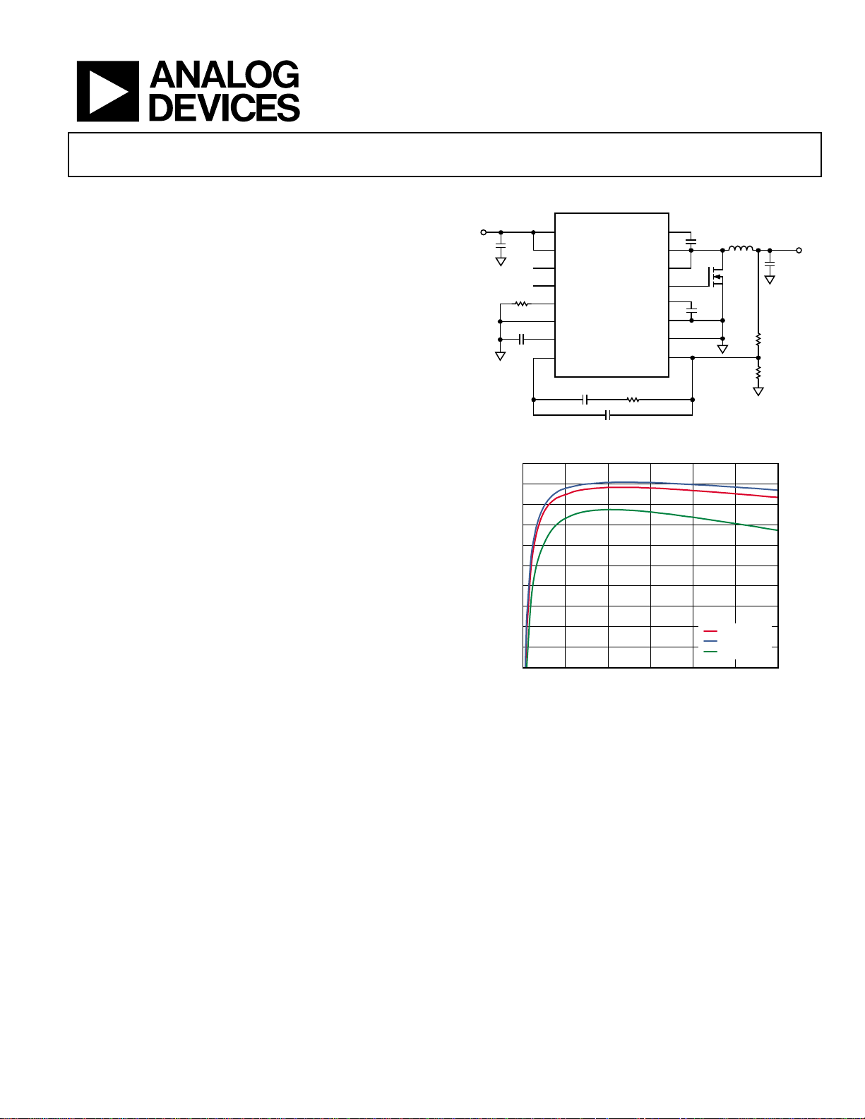
20 V, 6 A Synchronous Step-Down
TYPICAL APPLICATIONS CIRCUIT
Figure 1.
GENERAL DESCRIPTION
The ADP2381 is a current mode control, synchronous, stepdown, dc-to-dc regulator. It integrates a 44 mΩ power MOSFET
and a low-side driver to provide a high efficiency solution. The
ADP2381 runs from an input voltage of 4.5 V to 20 V and can
deliver 6 A of output current. The output voltage can be
adjusted to 0.6 V to 90% of the input voltage. The switching
frequency of the ADP2381 can be programmed from
250 kHz to 1.4 MHz or fixed at 290 kHz or 550 kHz. The
synchronization function allows the switching frequency to be
synchronized to an external clock to minimize system noise.
responsibility is assumed by Analog Devices for its use, nor for any infringements of patents or other
rights of third parties that may result from its use. Specifications subject to change without notice. No
license is granted by implication or otherwise under any patent or patent rights of Analog Devices.
External compensation and an adjustable soft start provide
design flexibility. The power-good output provides simple and
reliable power sequencing. Additional features include
programmable undervoltage lockout (UVLO), overvoltage
protection (OVP), overcurrent protection (OCP), and thermal
shutdown (TSD).
The ADP2381 operates over the −40°C to +125°C junction
temperature range and is available in a 16-lead TSSOP_EP
package.
One Technology Way, P.O. Box 9106, Norwood, MA 02062-9106, U.S.A.
Tel: 781.329.4700
Figure 2. ADP2381 Efficiency vs. Output Current, V
= 12 V, fSW = 250 kHz
IN
www.analog.com
Page 2

ADP2381 Data Sheet
TABLE OF CONTENTS
Features .............................................................................................. 1
Applications ....................................................................................... 1
Typical Applications Circuit ............................................................ 1
General Description ......................................................................... 1
Revision History ............................................................................... 2
Specifications ..................................................................................... 3
Absolute Maximum Ratings ............................................................ 5
Thermal Information ................................................................... 5
ESD Caution .................................................................................. 5
Pin Configuration and Function Description .............................. 6
Typical Performance Characteristics ............................................. 7
Functional Block Diagram ............................................................ 12
Theory of Operation ...................................................................... 13
Control Scheme .......................................................................... 13
Internal Regulator (VREG) ....................................................... 13
Bootstrap Circuitry .................................................................... 13
Low-Side Driver .......................................................................... 13
Oscillator ..................................................................................... 13
Synchronization .......................................................................... 13
Enable and Soft Start .................................................................. 13
Power Good ................................................................................. 14
Peak Current Limit and Short-Circuit Protection ................. 14
Overvoltage Protection (OVP) ................................................. 14
Undervoltage Lockout (UVLO) ................................................ 14
Thermal Shutdown ..................................................................... 14
Applications Information .............................................................. 15
Input Capacitor Selection .......................................................... 15
Output Voltage Setting .............................................................. 15
Voltage Conversion Limitations ............................................... 15
Inductor Selection ...................................................................... 15
Output Capacitor Selection....................................................... 17
Low-Side Power Device Selection ............................................ 17
Programming Input Voltage UVLO ........................................ 18
Compensation Design ............................................................... 18
ADIsimPower Design Tool ....................................................... 19
Design Example .............................................................................. 20
Output Voltage Setting .............................................................. 20
Frequency Setting ....................................................................... 20
Inductor Selection ...................................................................... 20
Output Capacitor Selection....................................................... 20
Low-Side MOSFET Selection ................................................... 21
Compensation Components ..................................................... 21
Soft Start Time Program ........................................................... 21
Input Capacitor Selection .......................................................... 21
Schematic for Design Example ................................................. 21
External Components Recommendation .................................... 23
Circuit Board Layout Recommendations ................................... 25
Typical Application Circuits ......................................................... 27
Outline Dimensions ....................................................................... 28
Ordering Guide .......................................................................... 28
REVISION HISTORY
3/12—Revision 0: Initial Version
Rev. 0 | Page 2 of 28
Page 3

Data Sheet ADP2381
PVIN
SHDN
EA Source Current
I
SOURCE
40
60
80
µA
SINK
VREG
PVIN
VREG
PVIN
VREG
BST
MIN_ON
SW Minimum Off Time
t
MIN_OFF
200
300
ns
BOOT
OSCILLATOR (RT PIN)
OSC
SS_UP
SPECIFICATIONS
VIN = 12 V, TJ = −40°C to +125°C for min/max specifications, and TA = 25°C for typical specifications, unless otherwise noted.
Table 1.
Parameter Symbol Test Conditions/Comments Min Typ Max Unit
PVIN
PVIN Voltage Range V
Quiescent Current IQ No switching 2 2.8 3.5 mA
Shutdown Current I
PVIN Undervoltage Lockout Threshold PVIN rising 4.3 4.5 V
FB
FB Regulation Voltage VFB 0°C < TJ < 85°C 0.594 0.6 0.606 V
FB Bias Current IFB 0.01 0.1 µA
ERROR AMPLIFIER (EA)
Transconductance gm 360 500 620 µS
4.5 20 V
EN/SS = GND 80 130 170 µA
PVIN falling 3.7 3.9 V
−40°C < TJ < +125°C 0.591 0.6 0.609 V
EA Sink Current I
40 60 80 µA
INTERNAL REGULATO R (VREG)
VREG Voltage V
Dropout Voltage V
V
= 12 V, I
= 12 V, I
= 50 mA 7.6 8 8.4 V
= 50 mA 350 mV
Regulator Current Limit 65 100 135 mA
SW
High-Side On Resistance1 V
− VSW = 5 V 44 70 mΩ
High-Side Peak Current Limit 7.7 9.6 11.5 A
Negative Current-Limit Threshold Voltage2 20 mV
SW Minimum On Time t
120 170 ns
LOW-SIDE DRIVER (LD)
Rising Time2 tR CDL = 2.2 nF; see Figure 17 20 ns
Falling Time2 tF CDL = 2.2 nF; see Figure 20 10 ns
Sourcing Resistor 4 6 Ω
Sinking Resistor 2 3.5 Ω
BST
Bootstrap Voltage V
Switching Frequency
4.5 5 5.7 V
fSW RT pin connected to GND 210 290 360 kHz
RT pin open 400 550 690 kHz
R
= 100 kΩ 425 500 570 kHz
Switching Frequency Range fSW 250 1400 kHz
SYNC
Synchronization Range 250 1400 kHz
SYNC Minimum Pulse Width 100 ns
SYNC Minimum Off Time 100 ns
SYNC Input High Voltage 1.3 V
SYNC Input Low Voltage 0.4 V
EN/SS
Enable Threshold 0.5 V
Internal Soft Start 1500 Clock cycles
SS Pin Pull-Up Current I
2.6 3.3 4 µA
Rev. 0 | Page 3 of 28
Page 4
ADP2381 Data Sheet
PGOOD from high to low
16 Clock cycles
PGOOD
PGOOD
THERMAL
Parameter Symbol Test Conditions/Comments Min Typ Max Unit
POWER GOOD (PGOOD)
PGOOD Range FB rising threshold 95 %
FB falling threshold 90 %
PGOOD Deglitch Time PGOOD from low to high 1024 Clock cycles
PGOOD Leakage Current V
PGOOD Output Low Voltage I
= 5 V 0.01 0.1 µA
= 1 mA 125 200 mV
UVLO
Rising Threshold 1.2 1.28 V
Falling Threshold 1.02 1.1 V
Thermal Shutdown Threshold 150
Thermal Shutdown Hysteresis 25
1
Pin-to-pin measurement.
2
Guaranteed by design.
°C
°C
Rev. 0 | Page 4 of 28
Page 5
Data Sheet ADP2381
SW
−1 V to +22 V
Storage Temperature Range
−65°C to +150°C
Package Type
θ
JA
Unit
ABSOLUTE MAXIMUM RATINGS
Table 2.
Parameter Rating
PVIN, PGOOD −0.3 V to +22 V
BST VSW + 6 V
UVLO, FB, EN/SS, COMP, SYNC, RT
VREG, LD −0.3 V to +12 V
PGND to GND −0.3 V to +0.3 V
Operating Junction Temperature Range −40°C to +125°C
Soldering Conditions JEDEC J-STD-020
Stresses above those listed under Absolute Maximum Ratings
may cause permanent damage to the device. This is a stress
rating only; functional operation of the device at these or any
other conditions above those indicated in the operational
section of this specification is not implied. Exposure to absolute
maximum rating conditions for extended periods may affect
device reliability.
−0.3 V to +6 V
Absolute maximum ratings apply individually only, not in
combination. Unless otherwise specified, all other voltages are
referenced to GND.
THERMAL INFORMATION
Table 3. Thermal Resistance
16-lead TSSOP_EP 39.48 °C/W
θJA is specified for the worst-case conditions, that is, a device
soldered in circuit board (4-layer, JEDEC standard board) for
surface-mount packages.
ESD CAUTION
Rev. 0 | Page 5 of 28
Page 6
ADP2381 Data Sheet
OUT
12
VREG
Internal 8 V Regulator Output. Place a 1 µF ceramic capacitor between this pin and GND.
TOP VIEW
(Not to S cale)
1
2
3
4
5
6
7
8
ADP2381
16
15
14
13
12
11
10
9
PVIN
UVLO
PGOOD
EN/SS
SYNC
RT
PVIN
SW
SW
LD
GND
COMP FB
PGND
VREG
BST
10209-003
NOTES
1. THE EXPOSED PAD SHOULD BE SOLDERED
TO AN EXT E RNAL GROUND PLANE UNDE RNE ATH
THE IC FOR THERMAL DISSIPATION.
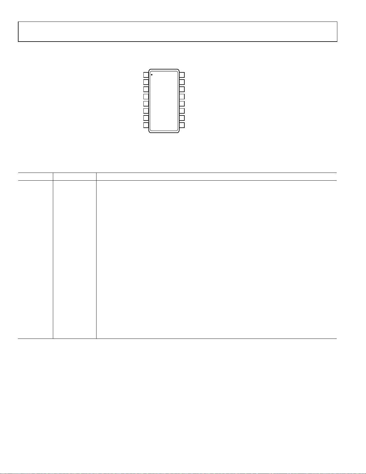
PIN CONFIGURATION AND FUNCTION DESCRIPTION
Figure 3. Pin Configuration (Top View)
Table 4. Pin Function Descriptions
Pin No. Mnemonic Description
1, 2 PVIN Power Input. Connect to the input power source and connect a bypass capacitor between this pin and
PGND.
3 UVLO Undervoltage Lockout Pin. An external resistor divider can be used to set the turn-on threshold.
4 PGOOD Power-Good Output (Open Drain). A pull-up resistor of 10 kΩ to 100 kΩ is recommended.
5 RT Frequency Setting. Connect a resistor between RT and GND to program the switching frequency
between 250 kHz and 1.4 MHz. If the RT pin is connected to GND, the switching frequency is set to 290
kHz. If the RT pin is open, the switching frequency is set to 550 kHz.
6 SYNC Synchronization Input. Connect this pin to an external clock to synchronize the switching frequency
between 250 kHz and 1.4 MHz (see the Oscillator section and the Synchronization section for details).
7 EN/SS Enable Pin (EN). When this pin voltage falls below 0.5 V, the regulator is disabled.
Soft Start (SS). This pin can also be used to set the soft start time.
Connect a capacitor from SS to GND to program the slow soft start time. If this pin is open, the regulator
is enabled and uses the internal soft start.
8 COMP Error Amplifier Output. Connect an RC network from COMP to FB.
9 FB Feedback Voltage Sense Input. Connect to a resistor divider from V
.
10 GND Analog Ground. Connect to the ground plane.
11 PGND Power Ground. Connect to the source of the synchronous N-channel MOSFET.
13 LD Low-Side Gate Driver Output. Connect this pin to the gate of the synchronous N-MO SFET.
14, 15 SW Switch Node Output. Connect this pin to the output inductor.
16 BST Supply Rail for the High-Side Gate Drive. Place a 0.1 µF ceramic capacitor between SW and BST.
17 EPAD The exposed pad should be soldered to an external ground plane underneath the IC for thermal
dissipation.
Rev. 0 | Page 6 of 28
Page 7
Data Sheet ADP2381
100
50
55
60
65
70
75
80
85
90
95
0 1 2 3 4 5 6
EFFICIENCY (%)
OUTPUT CURRE NT (A)
10209-004
V
OUT
= 1.2V
V
OUT
= 1.8V
V
OUT
= 2.5V
V
OUT
= 3.3V
V
OUT
= 5V
INDUCTOR: FDVE1040-2R2M
MOSFET: FDS6298
100
50
55
60
65
70
75
80
85
90
95
0 1 2 3 4 5 6
EFFICIENCY (%)
OUTPUT CURRE NT (A)
10209-005
V
OUT
= 1.8V
V
OUT
= 2.5V
V
OUT
= 3.3V
V
OUT
= 5V
INDUCTOR: FDVE1040-3R3M
MOSFET: FDS6298
10209-006
90
100
110
120
130
140
150
160
4 6 8 10 12 14 16 18 20
SHUTDOWN CURRENT (μA)
VIN (V)
TJ = –40°C
TJ = +25°C
TJ = +125°C
100
50
55
60
65
70
75
80
85
90
95
0 1 2 3 4 5 6
EFFICIENCY (%)
OUTPUT CURRE NT (A)
10209-007
V
OUT
= 1.2V
V
OUT
= 1.8V
V
OUT
= 2.5V
V
OUT
= 3.3V
V
OUT
= 5V
INDUCTOR: FDVE1040-4R7M
MOSFET: FDS6298
100
50
55
60
65
70
75
80
85
90
95
0 1 2 3 4 5 6
EFFICIENCY (%)
OUTPUT CURRE NT (A)
10209-008
V
OUT
= 1.0V
V
OUT
= 1.2V
V
OUT
= 1.5V
V
OUT
= 1.8V
V
OUT
= 2.5V
V
OUT
= 3.3V
INDUCTOR: 744 333 0100
MOSFET: FDS6298
1.80
2.00
2.20
2.40
2.60
2.80
3.00
3.20
4 6 8 10 12 14 16 18 20
QUIESCENT CURRENT (mA)
VIN (V)
10209-009
TJ = –40°C
T
J
= +25°C
TJ = +125°C
TYPICAL PERFORMANCE CHARACTERISTICS
Operating conditions: TA = 25oC, VIN = 12 V, V
= 3.3 V, L = 2.2 µH, C
OUT
= 2 × 100 µF, fSW = 500 kHz, unless otherwise noted.
OUT
Figure 4. Efficiency at VIN = 12 V, fSW = 500 kHz
Figure 5. Efficiency at VIN = 18 V, fSW = 500 kHz
Figure 7. Efficiency at VIN = 12 V, fSW = 250 kHz
Figure 8. Efficiency at VIN = 5 V, fSW = 500 kHz
Figure 6. Shutdown Current vs. VIN
Figure 9. Quiescent Current vs. VIN
Rev. 0 | Page 7 of 28
Page 8
ADP2381 Data Sheet
4.5
PVIN UVLO THRESHOLD (V)
10209-011
3.30
2.90
–40 120
SS PULL- UP CURRE NT (µA)
TEMPERATURE (°C)
2.95
3.00
3.05
3.10
3.15
3.20
3.25
–20 0 20 40 60 80 100
530
520
510
470
480
490
500
–40 120
FREQUENCY ( kHz )
TEMPERATURE (°C)
10209-012
–20 0 20 40 60 80 100
R
OSC
= 100kΩ
10209-013
1.00
1.30
–40 –20 0 20 40 60 80 100 120
UVLO PI N THRESHOLD (V )
TEMPERATURE (°C)
1.05
1.10
1.15
1.20
1.25
RISING
FALLING
606
604
602
594
596
598
600
–40 120
FEEDBACK VOLTAGE (mV)
TEMPERATURE (°C)
10209-014
–20 0 20 40 60 80 100
10209-015
8.4
7.6
–40 120
VREG VOLTAGE (V)
TEMPERATURE (°C)
7.7
7.8
7.9
8.0
8.1
8.2
8.3
–20 0 20 40 60 80 100
4.4
4.3
4.2
4.1
4.0
3.9
3.8
3.7
3.6
–40 –20 0 20 40 60 80 100 120
RISING
FALLING
TEMPERATURE (°C)
Figure 10. PVIN UVLO Threshold vs. Temperature
10209-010
Figure 13. UVLO Pin Threshold vs. Temperature
Figure 11. SS Pin Pull-Up Current vs. Temperature
Figure 12. Frequency vs. Temperature
Figure 14. FB Voltage vs. Temperature
Figure 15. VREG Voltage vs. Temperature
Rev. 0 | Page 8 of 28
Page 9
Data Sheet ADP2381
70
60
20
30
40
50
–40 120
MOSFET R
DSON
(mΩ)
TEMPERATURE (°C)
10209-016
–20 0 20 40 60 80 100
10209-017
CH2 5.00VCH1 5.00V M20.0ns A CH2 3.70V
1
2
T 46.60%
SW
LD
10209-018
CH2 10V
CH4 2A Ω
CH1 10mV
B
W
M2.00µs A CH2 6.00V
4
2
1
T 50.00%
V
OUT
(AC)
I
L
SW
11.0
10.5
10.0
8.0
8.5
9.0
9.5
–40 120
PEAK CURRENT LIMIT THRE S HOLD (A)
TEMPERATURE (°C)
10209-019
–20 0 20 40 60 80 100
10209-020
CH2 5.00VCH1 5.00V M20.0ns A CH2 3.70V
1
2
T 43.80%
SW
LD
10209-021
CH2 5.00V
CH4 5.00A Ω
CH1 2.00V
CH3 5.00V
M2.00ms A CH2 5.80V
1
3
2
4
T 50.00%
EN/SS
PGOOD
V
OUT
I
OUT
B
W
Figure 16. MOSFET R
vs. Temperature
DSON
Figure 17. Low-Side Driver Rising Edge Waveform, CDL = 2.2 nF
Figure 19. Current-Limit Threshold vs. Temperature
Figure 20. Low-Side Driver Falling Edge Waveform, CDL = 2.2 nF
Figure 18. Working Mode Waveform
Figure 21. Soft Start with Full Load
Rev. 0 | Page 9 of 28
Page 10

ADP2381 Data Sheet
10209-022
CH2 5.00V
CH4 5.00A Ω
CH1 2.00V
CH3 5.00V
M2.00ms A CH2 2.00V
1
3
2
4
T 49.60%
EN/SS
PGOOD
V
OUT
I
L
B
W
10209-023
CH1 100mV M200µs A CH4 2.52 A
1
4
T 70.20%
CH4 2.00A Ω
V
OUT
(AC)
I
OUT
B
W
10209-024
CH2 10.0V
CH4 5.00A Ω
CH1 2.00V M10.00ms A CH1 1.96V
1
2
4
T 30.40%
V
OUT
SW
I
L
B
W
10209-025
CH2 10.0V
M1.00µs A CH2 7.00V
3
2
T 50.00%
CH3 5.00V
SYNC
SW
B
W
10209-026
CH2 10.0VCH1 20.0mV
CH3 5.00V
M1.00ms A CH3 13.5V
1
2
3
T 20.20%
V
OUT
(AC)
SW
V
IN
I
L
B
W
B
W
B
W
10209-027
CH2 10.0V
CH4 5.00A Ω
CH1 2.00V M10.00ms A CH1 1.96V
1
2
4
T 60.40%
V
OUT
SW
I
L
B
W
Figure 22. Precharged Output
Figure 23. Load Transient Response, 1 A to 5 A
Figure 25. External Synchronization
Figure 26. Line Transient Response, VIN from 10 V to 16 V, I
OUT
= 6 A
Figure 24. Output Short Entry
Figure 27. Output Short Recovery
Rev. 0 | Page 10 of 28
Page 11

Data Sheet ADP2381
7
0
1
2
3
4
5
6
25 40 55 70 85 100
LOAD CURRENT ( A)
AMBIENT T E M P E RATURE (°C)
10209-028
V
OUT
= 1.2V
V
OUT
= 1.8V
V
OUT
= 2.5V
V
OUT
= 3.3V
V
OUT
= 5V
7
0
1
2
3
4
5
6
25 40 55 70 85 100
LOAD CURRENT ( A)
AMBIENT T E M P E RATURE (°C)
10209-029
V
OUT
= 1V
V
OUT
= 1.2V
V
OUT
= 1.8V
V
OUT
= 2.5V
V
OUT
= 3.3V
V
OUT
= 5V
Figure 28. Load Current vs. Ambient Temperature, VIN = 12 V,
f
= 500 kHz
SW
Figure 29. Load Current vs. Ambient Temperature, VIN = 12 V,
f
= 250 kHz
SW
Rev. 0 | Page 11 of 28
Page 12

ADP2381 Data Sheet
ADP2381
OSCILLATOR
RT
SYNC
UVLO
CLK
SLOPE RAMP
CONTROL
LOGIC
AND MOSFET
DRIVER WI TH
ANTICROSS
PROTECTION
PGOOD
GND
UVLO
SLOPE RAMP
LD
PGND
+
–
+
0.6V
I
SS
EN/SS
FB
AMP
COMP
0.7V
0.54V
1.2V
OVP
CLK
+
–
+
–
+
–
Σ
I
MAX
HICCUP
MODE
CMP
OCP
+
–
+
–
SW
NFET
BST
DRIVER
VREG
DRIVER
BOOST
REGULATOR
DEGLITCH
BIAS AND DRIVER
REGULATOR
+
–
A
CS
PVIN
VREG
320kΩ
125kΩ
PVIN
10209-030
NEGATIVE
CURRENT LIM IT
CMP
+
–
FUNCTIONAL BLOCK DIAGRAM
Figure 30. Functional Block Diagram
Rev. 0 | Page 12 of 28
Page 13

Data Sheet ADP2381
15]kΩ[
600,57
]
kHz[
+
=
OSC
SW
R
f
)ms(
]kHz[
1500
_SWINTSS
f
t =
UPSS
SS
EXTSS
I
C
t
_
_
V6.0 ×
=
1400
1200
1000
800
600
400
200
0
20 60 100 140 180 220 260 300
SWITCHING FREQUE NCY ( kHz )
R
OSC
(kΩ)
10209-031
THEORY OF OPERATION
The ADP2381 is a synchronous, step-down, dc-to-dc regulator.
It uses current-mode architecture with an integrated high-side
power switch and a low-side driver. It targets high performance
applications that require high efficiency and design flexibility.
The ADP2381 can operate with an input voltage from 4.5 V to
20 V and regulate the output voltage down to 0.6 V. Additional
features for design flexibility include programmable switching
frequency, soft start, external compensation, and power-good pin.
CONTROL SCHEME
The ADP2381 uses fixed frequency, peak current-mode PWM
control architecture. At the start of each oscillator cycle, the
high-side N-MOSFET is turned on, putting a positive voltage
across the inductor. Current in the inductor increases until
the current sense signal crosses the peak inductor current threshold that turns off the high-side N-MOSFET and turns on the
low-side N-MOSFET. This puts a negative voltage across the
inductor, causing the inductor current to decrease. The lowside N-MOSFET stays on for the rest of the cycle.
INTERNAL REGULATOR (VREG)
The internal regulator provides a stable supply for the internal
circuits and provides bias voltage for the low-side gate driver.
Placing a 1 µF ceramic capacitor between VREG and GND is
recommended. The internal regulator also includes a currentlimit circuit to protect the circuit if the maximum external
load is added.
BOOTSTRAP CIRCUITRY
The ADP2381 has integrated the boot regulator to provide the
gate drive voltage for the high-side N-MOSFET. It generates a
5 V bootstrap voltage between BST and SW by differential
sensing.
It is recommended to place a 0.1 µF, X7R or X5R ceramic
capacitor between the BST pin and the SW pin.
A 100 kΩ resistor sets the frequency to 500 kHz, and a 215 kΩ
resistor sets the frequency to 250 kHz. Figure 31 shows the typical
relationship between f
Figure 31. Switching Frequency vs. R
and R
SW
OSC
.
OSC
SYNCHRONIZATION
To synchronize the ADP2381, connect an external clock to the
SYNC pin. The frequency of the external clock can be in the
range of 250 kHz to 1.4 MHz. During synchronization, the
switching rising edge runs 180° out of phase with the external
clock rising edge.
When the ADP2381 is being synchronized, connect a resistor
from the RT pin to GND to program the internal oscillator to
run at 90% to 110% of the external synchronization clock.
ENABLE AND SOFT START
When the voltage of the EN/SS pin exceeds 0.5 V, t he ADP2381
starts operation.
The ADP2381 has an internal digital soft start. The internal soft
start time can be calculated by using the following equation:
LOW-SIDE DRIVER
The LD pin provides the gate driver for the low-side N-channel
MOSFET. Internal circuitry monitors the external MOSFET to
ensure break-before-make switching to prevent cross
conduction.
OSCILLATOR
The ADP2381 switching frequency is controlled by the RT pin.
If the RT pin is connected to GND, the switching frequency is
set to 290 kHz. If the RT pin is open, the switching frequency is
set to 550 kHz. A resistor connected from RT to GND can
program the switching frequency according to the following
equation:
A slow soft start time can be programmed by the EN/SS pin.
Place a capacitor between the EN/SS pin and GND. An internal
current charges this capacitor to establish the soft start ramp.
The soft start time can be calculated by using the following
equation:
where:
C
is the soft start capacitance.
SS
I
is the soft start pull-up current (3.3 µA).
SS_UP
The internal error amplifier includes three positive inputs: the
internal reference voltage, the internal digital soft start voltage,
and the EN/SS voltage. The error amplifier regulates the FB
voltage to the lowest of the three voltages.
Rev. 0 | Page 13 of 28
Page 14

ADP2381 Data Sheet
If the output voltage is charged prior to turn-on, the ADP2381
prevents the low-side MOSFET from turning on, which
discharges the output voltage until the soft start voltage exceeds
the voltage on the FB pin.
When the regulator is disabled or a current fault happens, the
soft start capacitor is discharged, and the internal digital soft
start is reset to 0 V.
POWER GOOD
The power-good (PGOOD) pin is an active high, open-drain
output that requires a pull-up resistor. A logic high indicates
that the voltage at the FB pin (and, therefore, the output
voltage) is above 95% of the reference voltage and there is a
1024 cycle waiting period before PGOOD is pulled high. A logic
low indicates that the voltage at the FB pin is below 90% of the
reference voltage and there is a 16-cycle waiting period before
PGOOD is pulled low.
PEAK CURRENT LIMIT AND SHORT-CIRCUIT PROTECTION
The ADP2381 has a peak current-limit protection circuit to
prevent current runaway. During soft start, the ADP2381 uses
frequency foldback to prevent output current runaway. The
switching frequency is reduced according to the voltage on the
FB pin, which allows more time for the inductor to discharge.
The correlation between the switching frequency and FB pin
voltage is shown in Tab l e 5.
Table 5. Switching Frequency and FB Pin Voltage
FB Pin Voltage Switching Frequency
VFB ≥ 0.4 V fSW
0.4 V > VFB ≥ 0.2 V fSW/2
VFB < 0.2 V
For heavy load protection, the ADP2381 uses hiccup mode for
overcurrent protection. When the inductor peak current reaches
the current-limit value, the high-side MOSFET turns off and
the low-side driver turns on until the next cycle, while the
overcurrent counter increments. If the overcurrent counter
reaches 10, or the FB pin voltage falls to ≤0.4 V after the soft
start, the regulator enters hiccup mode. The high-side MOSFET
and low-side MOSFET are both turned off. The regulator
remains in this mode for 4096 clock cycles and then attempts to
fSW/4
restart. If the current limit fault is cleared, the regulator resumes
normal operation. Otherwise, it reenters hiccup mode.
The ADP2381 also provides a sink current limit to prevent the
low-side MOSFET from sinking a lot of current from the load.
When the voltage across the low-side MOSFET exceeds the
sink current-limit threshold, which is typically 20 mV, the lowside MOSFET turns off immediately for the rest of this cycle.
Both high-side and low-side MOSFETs turn off until the next
clock cycle.
In some cases, the input voltage (PVIN) ramp rate is too slow or
the output capacitor is too large to support the setting regulation
voltage during the soft start, causing the regulator to enter
hiccup mode. To avoid such cases, use a resistor divider at the
UVLO pin to program the UVLO input voltage, or use a longer
soft start time.
OVERVOLTAGE PROTECTION (OVP)
The ADP2381 provides an overvoltage protection feature to
protect the system against an output shorting to a higher voltage
supply or a strong load transient occurring. If the feedback
voltage increases to 0.7 V, the internal high-side MOSFET and
low-side driver are turned off until the voltage at FB decreases to
0.63 V. At that time, the ADP2381 resumes normal operation.
UNDERVOLTAGE LOCKOUT (UVLO)
The UVLO pin enable threshold is 1.2 V with 100 mV
hysteresis.
The ADP2381 has an internal voltage divider consisting of two
resistors from PVIN to GND, 320 kΩ for the high-side resistor
and 125 kΩ for the low-side resistor. An external resistor divider
from PVIN to GND can be used to override the internal resistor
divider.
THERMAL SHUTDOWN
In the event that the ADP2381 junction temperatures rise above
150°C, the thermal shutdown circuit turns off the regulator.
Extreme junction temperatures can be the result of high current
operation, poor circuit board design, and/or high ambient
temperature. A 25°C hysteresis is included so that when thermal
shutdown occurs, the ADP2381 does not return to operation
until the on-chip temperature drops below 125°C. Upon
recovery, soft start is initiated prior to normal operation.
Rev. 0 | Page 14 of 28
Page 15

Data Sheet ADP2381
)1(_DDII
OUT
RMSC
IN
−××=
+×=
BOT
TOP
OUT
R
R
V 16.0
OUT
TOP
BOT
2.5
47.5
15
( )
D
fI
VV
L
SW
L
OUT
IN
×
×∆
−
=
IN
OUT
V
V
D =
APPLICATIONS INFORMATION
INPUT CAPACITOR SELECTION
The input decoupling capacitor is used to attenuate high
frequency noise on the input. This capacitor should be a
ceramic capacitor in the range of 10 µF to 47 µF. It should be
placed close to the PVIN pin. The loop composed by this input
capacitor, high-side NFET, and low-side NFET must be kept as
small as possible.
The voltage rating of the input capacitor must be greater than
the maximum input voltage. The rms current rating of the input
capacitor should be larger than the following equation:
OUTPUT VOLTAGE SETTING
The output voltage of ADP2381 can be set by an external
resistive divider using the following equation:
To limit output voltage accuracy degradation due to FB bias
current (0.1 µA maximum) to less than 0.5% (maximum),
ensure that R
is less than 30 kΩ.
BOT
Table 6 gives the recommended resistor divider values for
various output voltage options.
Table 6. Resistor Divider for Different Output Voltages
V
(V) R
, ±1% (kΩ) R
, ±1% (kΩ)
1.0 10 15
1.2 10 10
1.5 15 10
1.8 20 10
3.3 10 2.21
5.0 22 3
VOLTAGE CONVERSION LIMITATIONS
The minimum output voltage for a given input voltage and
switching frequency is constrained by the minimum on time.
The minimum on time of the ADP2381 is typically 120 ns. The
minimum output voltage at a given input voltage and frequency
can be calculated using the following equation:
V
= VIN × t
OUT_MIN
× t
MIN_ON
× fSW – (R
where:
V
t
f
R
R
I
R
is the minimum output voltage.
OUT_MIN
is the minimum on time.
MIN_ON
is the switching frequency.
SW
is the high-side MOSFET on resistance.
DSON_HS
is the low-side MOSFET on resistance.
DSON_LS
is the minimum output current.
OUT_MIN
is the series resistance of the output inductor.
L
MIN_ON
DSON_LS
× fSW – (R
+ RL) × I
DSON_HS
OUT_MIN
– R
DSON_LS
) × I
OUT_MIN
(1)
The maximum output voltage for a given input voltage and
switching frequency is constrained by the minimum off time
and the maximum duty cycle. The minimum off time is
typically 200 ns, and the maximum duty cycle of the ADP2381
is typically 90%.
The maximum output voltage limited by the minimum off time
at a given input voltage and frequency can be calculated using
the following equation:
V
I
OUT_MAX
OUT_MAX
= VIN × (1 – t
× (1 – t
MIN_OFF
× fSW) – (R
MIN_OFF
× fSW) – (R
DSON_LS
– R
DSON_HS
+ RL) × I
DSON_LS
OUT_MAX
) ×
(2)
where:
V
t
I
is the maximum output voltage.
OUT_ MAX
is the minimum off time.
MIN_OFF
is the maximum output current.
OUT_ MAX
The maximum output voltage, limited by the maximum duty
cycle at a given input voltage, can be calculated by using the
following equation:
V
where D
= D
OUT_MAX
is the maximum duty.
MAX
× VIN (3)
MAX
As Equation 1 to Equation 3 show, reducing the switching
frequency alleviates the minimum on time and minimum off
time limitation.
INDUCTOR SELECTION
The inductor value is determined by the operating frequency,
input voltage, output voltage, and inductor ripple current. Using
a small inductor leads to a faster transient response, but it
degrades efficiency due to larger inductor ripple current,
whereas using a large inductor value leads to smaller ripple
current and better efficiency, but it results in a slower transient
response.
As a guideline, the inductor ripple current, ΔI
to 1/3 of the maximum load current. The inductor can be
calculated using the following equation:
where:
V
is the input voltage.
IN
V
is the output voltage.
OUT
ΔI
is the inductor current ripple.
L
f
is the switching frequency.
SW
D is the duty cycle.
The ADP2381 uses adaptive slope compensation in the current
loop to prevent subharmonic oscillations when
the duty cycle is larger than 50%. The internal slope
compensation limits the minimum inductor value.
, is typically set
L
Rev. 0 | Page 15 of 28
Page 16

ADP2381 Data Sheet
SW
OUT
fDV×−×2
)1(
2
L
OUT
PEAK
III∆
+=
12
2
2
L
OUT
RMS
III∆
+=
SAT
RMS
Vishay
IHLP3232DZ-R47M-11
0.47
14
25
2.38
IHLP4040DZ-3R3M-01
3.3
18.6
10
14.4
For a duty cycle that is larger than 50%, the minimum inductor
value is determined by the following equation:
quick saturation characteristic, the saturation current rating of
the inductor should be higher than the current-limit threshold of
the switch to prevent the inductor from becoming saturated.
The rms current of the inductor can be calculated by
The inductor peak current is calculated using the following
equation:
Shielded ferrite core materials are recommended for low core
loss and low EMI. Table 7 lists some recommended inductors.
The saturation current of the inductor must be larger than the
peak inductor current. For the ferrite core inductors with a
Table 7. Recommended Inductors
Vendor Part No. Value (µH) I
(A) I
(A) DCR (mΩ)
Toko FDVE0630-R47M 0.47 15.6 14.1 3.7
FDVE0630-R75M 0.75 10.9 10.7 6.2
FDVE0630-1R0M 1.0 9.5 9.5 8.5
FDVE1040-1R5M 1.5 13.7 14.6 4.6
FDVE1040-2R2M 2.2 11.4 11.6 6.8
FDVE1040-3R3M 3.3 9.8 9.0 10.1
FDVE1040-4R7M 4.7 8.2 8.0 13.8
IHLP3232DZ-R68M-11 0.68 14.5 22.2 3.22
IHLP3232DZ-1R0M-11 1.0 12 18.2 4.63
IHLP4040DZ-1R5M-01 1.5 27.5 15 5.8
IHLP4040DZ-2R2M-01 2.2 25.6 12 9
IHLP4040DZ-4R7M-01 4.7 17 9.5 16.5
Wurth Elektronik 744 325 120 1.2 25 20 1.8
744 325 180 1.8 18 16 3.5
744 325 240 2.4 17 14 4.75
744 325 330 3.3 15 12 5.9
744 325 420 4.2 14 11 7.1
Rev. 0 | Page 16 of 28
Page 17

Data Sheet ADP2381
( )
UVOUTOUT
IN
STEP
UV
UVOUT
VVV
LIK
C
_
2
_
2 ∆×−×
×∆×
=
( )
2
2
_
2
_
OUTOVOUTOUT
STEP
OV
OVOUT
VVV
LIK
C
−∆+
×∆×
=
RIPPLEOUT
SW
L
RIPPLEOUT
Vf
I
C
_
_
8 ∆××
∆
=
L
RIPPLEOUT
ESR
I
V
R
∆
∆
=
_
12
_LRMSC
I
I
OUT
∆
=
DSON
Fairchild
FDS6298
30
13
12
10
OUTPUT CAPACITOR SELECTION
The output capacitor selection affects both the output ripple
voltage and the loop dynamics of the regulator.
During a load step transient on the output, for example, when
the load is suddenly increased, the output capacitor supplies the
load until the control loop has a chance to ramp up the inductor
current, which causes the output to undershoot. The output
capacitance required to satisfy the voltage droop requirement
can be calculated using the following equation:
where:
K
is a factor typically of 2.
UV
ΔI
is the load step.
STEP
ΔV
Another case occurs when a load is suddenly removed from the
output. The energy stored in the inductor rushes into the
capacitor, which causes the output to overshoot. The output
capacitance required to meet the overshoot requirement can be
calculated using the following equation:
where:
K
ΔV
The output ripple is determined by the ESR and the capacitance. Use the following equation to select a capacitor that can
meet the output ripple requirements:
is the allowable undershoot on the output voltage.
OUT_UV
is a factor typically of 2.
OV
is the allowable undershoot on the output voltage.
OUT_ OV
Select the largest output capacitance given by C
and C
OUT_RIPPLE
to meet both load transient and output ripple
performance.
The selected output capacitor voltage rating should be greater
than the output voltage. The rms current rating of the output
capacitor should be larger than the following equation:
LOW-SIDE POWER DEVICE SELECTION
The ADP2381 has an integrated low-side MOSFET driver that
drives the low-side NFET. The selection of the low-side NFET
affects the dc-to-dc regulator performance.
The selected MOSFET must meet the following requirements:
• Drain-source voltage (V
1.2 × V
• Drain current (I
.
IN
) must be greater than 1.2 × I
D
which is the selected maximum current-limit threshold.
• The ADP2381 low-side gate drive voltage is 8 V. Make sure
that the selected MOSFET can fully turn on at 8 V. Total
gate charge (Q
at 8 V) must be less than 50 nC. Lower Qg
g
characteristics constitute higher efficiency.
• The low-side MOSFET carries the inductor current when
the high-side MOSFET is turned off. For low duty cycle
application, the low-side MOSFET carries the output
current during most of the period. To achieve higher
efficiency, it is important to select a low on-resistance
MOSFET. The power conduction loss of the low-side
MOSFET can be calculated by using the following
equation:
P
= I
FET_LOW
where R
OUT
is the on resistance of the low-side MOSFET.
DSON
• Make sure that the MOSFET can handle the thermal
dissipation due to the power loss.
) must be higher than
DS
2
× R
× (1 – D)
DSON
OUT_UV
, C
OUT_OV
LIMIT_MAX
,
,
where:
ΔV
OUT_RIPPLE
R
ESR
is the allowable output ripple voltage.
is the equivalent series resistance of the output capacitor.
Some recommended MOSFETs are listed in Table 8.
Table 8. Recommended MOSFETs
Vendor Part No. VDS (V) ID (A) R
(mΩ) Qg (nC)
Fairchild FDS8880 30 10.7 12 12
Fairchild FDM7578 25 14 8 8
Vishay SiA430DJ 20 10.8 18.5 5.3
AOS AON7402 30 39 15 7.1
AOS AO4884L 40 10 16 13.6
Rev. 0 | Page 17 of 28
Page 18

ADP2381 Data Sheet
( )
V2.1
V2.1
_
R2V
R1
RISINGIN
×−
=
V1.1
2
V1.1
_
+
×
=
R
R1
V
FALLINGIN
P
Z
VI
COMP
OUT
VD
f
s
f
s
RA
sV
sV
sG
××
+
××
+
××==
π
π
2
1
2
1
)(
)(
)(
OUT
ESR
Z
CRf×××
=
π
2
1
OUT
ESR
P
CRR
f
×+××
=
)(2
1
π
)(
1
1
)( sG
s
CC
CCR
s
sCR
CC
g
RR
R
sT
VD
CPC
CPCC
CC
CPC
m
TOPBOT
BOT
V
×
×
+
××
+×
××+
×
+
−
×
+
=
VI
m
REF
C
OUTOUT
C
AgV
fCV
R
××
××××
=
π
2
C
OUT
ESR
C
R
CRR
C×+=
)(
PVINVIN
R1
R2
UVLO
320kΩ
125kΩ
ADP2381
10209-032
R
R
V
V
PROGRAMMING INPUT VOLTAGE UVLO
The internal voltage divider from PVIN to GND sets the default
start/stop values of the input voltage to achieve undervoltage
lockout (UVLO) performance. The default rising/falling
threshold of PVIN and UVLO are listed in Table 9. These
default values can be replaced by using an external voltage
divider to achieve a more accurate externally adjustable UVLO,
as shown in Figure 32. Lower values of the external resistors are
recommended to obtain a high accuracy UVLO threshold
because the values of the internal 320 kΩ and 125 kΩ resistors
may vary by as much as 20%.
Table 9. Default Rising/Falling Voltage Threshold
Pin Rising Threshold (V) Falling Threshold (V)
PVIN 4.28 3.92
UVLO 1.2 1.1
where:
AVI = 8.7 A/V.
R is the load resistance.
C
is the output capacitance.
OUT
R
is the equivalent series resistance of the output capacitor.
ESR
The external voltage loop is compensated by a transconductance amplifier with a simple external RC network placed either
between COMP and GND or between COMP and FB, as shown
in Figure 33 and Figure 34, respectively.
Compensation Network Between COMP and GND
Figure 33 shows the simplified peak current mode control small
signal circuit with a compensation network placed between
COMP and GND.
OUT
OUT
Figure 32. External Programmable UVLO
A 1 kΩ resistor for R2 is an appropriate choice. Use the
following equation to obtain the value of R1 for a chosen input
voltage rising threshold:
where V
is the rising threshold of VIN.
IN_RISING
The falling threshold of VIN can be determined by the
following equation:
where V
is the falling threshold of VIN.
IN_FALLING
COMPENSATION DESIGN
The ADP2381 uses a peak current-mode control architecture
for excellent load and line transient response. For peak currentmode control, the power stage can be simplified as a voltage
controlled current source, supplying current to the output
capacitor and load resistor. It consists of one domain pole and
one zero contributed by the output capacitor ESR.
The control to output transfer function is given by the following
equation:
TOP
BOT
Figure 33. Small Signal Circuit with Compensation Network Between COMP
ADP2381
FB
–
g
+
GND
COMP
V
COMP
m
R
C
C
C
C
CP
and GND
A
+
VI
C
OUT
–
R
ESR
R
10209-033
The RC and CC compensation components contribute a zero,
and the optional C
and RC contribute an optional pole.
CP
The closed-loop transfer function is as follows:
Use the following design guidelines to select the R
, CC, and CCP
C
compensation components:
• Determine the cross frequency, f
f
/12 and fSW/6.
SW
• R
can be calculated by
C
. Generally, fc is between
C
where:
V
= 0.6 V.
REF
g
= 500 µS.
m
• Place the compensation zero at the domain pole, f
be determined by:
. CC can
P
Rev. 0 | Page 18 of 28
Page 19

Data Sheet ADP2381
C
OUT
ESR
CP
R
CRC×
=
)1)(//)((
)(
)(
)1)(//(
__
____
___
___
__
__
0
m
BOTTOP
EACEACP
EACEACEACEACP
0
CCCCP
0
0
m
BOTTOP
EACPEACEAC
EACPEACEAC
0
CPCC
0
m
EACEACP
EACEACCC
rgRRCC
CRCCr
CRCCr
rgRRCCR
CCRrCCRr
g
CC
CRCR
×++
+++
=++
×+
+=
+
−=
BOTTOP
BOTTOP
BOTTOP
RR
RR
RR
+
=//
))((
))((
_
_
_
_
ArCRB
CCRr
C
C
CRB
R
ArCRB
CCRr
gBC
0
CC
CPCC
0
EACP
EAC
CC
EAC
0
CC
CPCC
0
m
EAC
++
=
+
=
+
+
−×=
)(1
)(
)1)(//(
0
m
CCP
0
0
m
BOTTOP
rAg
CCr
B
rgRRA
++
+
=
×+=
R
ESR
R
+
–
g
m
C
OUT
R
TOP
R
BOT
–
+
A
VI
V
OUT
V
COMP
V
OUT
10209-034
ADP2381
GND
COMP
FB
C
CP_EA
R
C_EA
C
C_EA
• C
is optional, and it can be used to cancel the zero caused
CP
by the ESR of the output capacitors.
where:
r
is the equivalent output impedance of the trans-conductance
0
amplifier, 40 MΩ.
Compensation Network Between COMP and FB
The compensation RC network can also be placed between
COMP and FB, as shown in Figure 34.
Figure 34. Small Signal Circuit with Compensation Network Between COMP
and FB
When connecting the compensation network as shown in
Figure 34, it should have the same pole and zero as in Figure 33
to maintain the same compensation performance.
Assuming that the compensation networks of Figure 33 and
Figure 34 have the same pole and zero,
Solve the preceding equations to obtain:
where:
ADIsimPower DESIGN TOOL
The ADP2381 is supported by the ADIsimPower™ design tool
set. ADIsimPower is a collection of tools that produce complete
power designs that are optimized for a specific design goal. The
tools enable the user to generate a full schematic and bill of
materials and calculate performance in minutes. ADIsimPower
can optimize designs for cost, area, efficiency, and parts count,
while taking into consideration the operating conditions and
limitations of the IC and all real external components. For more
information about the ADIsimPower design tools, visit
www.analog.com/ADIsimPower. The tool set is available from
this website, and users can request an unpopulated board.
Rev. 0 | Page 19 of 28
Page 20

ADP2381 Data Sheet
DESIGN EXAMPLE
This section provides the procedures of selecting the external
components based on the example specifications listed in Table 10.
The schematic of this design example is shown in Figure 36.
Table 10. Step-Down DC-to-DC Regulator Requirements
Parameter Specification
Input Voltage VIN = 12.0 V ± 10%
Output Voltage V
Output Current I
Output Voltage Ripple ∆V
OUT
= 6 A
OUT
OUT_RIPPLE
= 3.3 V
= 33 mV
Load Transient ±5%, 1 A to 5 A, 2 A/μs
Switching Frequency fSW = 500 kHz
OUTPUT VOLTAGE SETTING
Choose a 10 kΩ resistor as the top feedback resistor (R
calculate the bottom feedback resistor (R
) by using the
BOT
following equation:
RR
TOPBOT
V
OUT
6.0
6.0
To set the output voltage to 3.3 V, the resistors values are
= 10 kΩ, R
R
TOP
= 2.21 kΩ.
BOT
TOP
) and
FREQUENCY SETTING
Connect a 100 kΩ resistor from RT pin to GND to set the
switching frequency at 500 kHz.
INDUCTOR SELECTION
The peak-to-peak inductor ripple current, ΔIL, is set to 30% of
the maximum output current. Use the following equation to
estimate the inductor value:
DVV
OUT
L
IN
= 2.18 A.
L
OUT
fI
SW
OUT
fL
)(
SW
2
DVV
III
L
IN
L
where:
V
= 12 V.
IN
V
= 3.3 V.
OUT
D = V
Δ
I
= 1.8A.
L
f
= 500 kHz.
SW
OUT/VIN
= 0.275.
This results in L = 2.659 μH. Choose the standard inductor
value of 2.2 μH.
The peak-to-peak inductor ripple current can be calculated by
the following equation:
I
L
This results in ΔI
The peak inductor current can be calculated using the following
equation:
PEAK
This results in I
The rms current flowing through the inductor can be calculated
by the following equation:
RMS
This results in I
According to the calculated rms and peak inductor current
values, select an inductor with a minimum rms current rating of
6.03 A and a minimum saturation current rating of 7.09 A.
To protect the inductor from reaching its saturation limit, the
inductor should be rated for at least 9.6 A saturation current for
reliable operation.
Based on these requirements, select a 2.2 μH inductor, such as
the FDVE1040-2R2M from Toko, which has 6.8 mΩ DCR and
11.4 A saturation current.
OUTPUT CAPACITOR SELECTION
The output capacitor is required to meet both the output voltage
ripple requirement and the load transient response.
To meet the output voltage ripple requirement, use the
following equation to calculate the ESR and capacitance of the
output capacitor:
C
_
RIPPLEOUT
R
ESR
This results in C
To meet the ±5% overshoot and undershoot transient
requirements, use the following equations to calculate the
capacitance:
C
_
OVOUT
C
_
UVOUT
where:
K
= KUV = 2, the coefficients for estimation purposes.
OV
ΔI
= 4 A, the load transient step.
STEP
OUT_OV
OUT_UV
= 5%V
= 5%V
ΔV
ΔV
This results in C
According to the preceding calculation, the output capacitance
must be larger than 63 μF, and the ESR of the output capacitor
must be smaller than 15 mΩ. It is recommended that one 100
μF, X5R, 6.3 V ceramic capacitor and one 47 μF, X5R, 6.3 V
ceramic capacitor be used, such as the GRM32ER60J107ME20
and GRM32ER60J476ME20 from Murata with an ESR = 2 mΩ.
= 7.09 A.
PEAK
2
III
L
2
OUT
= 6.03 A.
RMS
8
V
_
I
L
OUT_RIPPLE
, the overshoot voltage.
OUT
, the undershoot voltage.
OUT
OUT_OV
12
I
L
Vf
SW
RIPPLEOUT
= 16.5 μF and R
OV
STEP
_
UV
STEP
IN
)(2
= 63.1 μF and C
_
2
2
)(
RIPPLEOUT
2
LIK
VVV
= 15.1 mΩ.
ESR
LIK
VVV
OUTOVOUTOUT
UVOUTOUT
_
OUT_UV
2
= 24.5 μF.
Rev. 0 | Page 20 of 28
Page 21

Data Sheet ADP2381
))((
))((
_
_
_
0
_
ArCRB
CCRr
C
C
CRB
R
ArCRB
CCRr
gBC
0
CC
CPCC
0
EACP
EAC
CC
EAC
0
CC
CPCC
m
EAC
++
=
+
=
++
−×=
kΩ3.37
/7.8μS500V6.0
kHz50μF943.32
2
=
××
××××
=
××
××××
=
VA
V
AgV
fCV
R
VI
m
REF
C
OUTOUT
C
π
π
nF39.1
kΩ3.37
μF94)002.0A6/V3.3(
)(
=
×Ω+
=
×+
=
C
OUT
ESR
C
R
CRR
C
pF04.5
kΩ3.37
μF94002.0
=
×Ω
=
×
=
C
OUT
ESR
CP
R
CR
C
( )
( )
7
1062.3MΩ40μS5001
kΩ21.2kΩ10
kΩ2.21kΩ10
1
×=×+
×
+
×
=×+
+
=
0
m
BOTTOP
BOTTOP
rg
RR
RR
A
6
7
1046.1
)MΩ401062.3(μS5001
)nF39.1pF04.5(MΩ40
)(1
)(
−
×
=
+××+
+×
=
++
+
=
0
m
CCP
0
rAg
CCr
B
nF22
V6.0
μA3.3ms4
6.0
_
_
=
×
=
×
=
UPSS
EXTSS
SS
It
C
60
48
36
24
12
0
–60
–48
–36
–24
–12
180
144
108
72
36
0
–180
–144
–108
–72
–36
1k 10k 100k 1M
MAGNITUDE ( dB)
PHASE (dB)
FREEQUENCY (Hz)
10209-035
LOW-SIDE MOSFET SELECTION
A low R
solution. The breakdown voltage of the MOSFET must be
higher than 1.2 × V
1.2 × I
It is recommended that a 30 V, N -channel MOSFET, such as the
FDS6298 from Fairchild, be used. The R
a 4.5 V driver voltage is 9.4 mΩ, and the total gate charge at 5 V
is 10 nC.
N-channel MOSFET is selected as a high efficiency
DSON
, and the drain current must be larger than
IN
.
LIMIT
of the FDS6298 at
DSON
COMPENSATION COMPONENTS
For a better load transient and stability performance, set the
cross frequency, f
50 kHz.
, at fSW/10. In this case, fC = 1/500 kHz =
C
This results in
R
= 73.3 kΩ.
C_EA
C
= 727.6 pF.
C_EA
C
= 2.56 pF.
CP_EA
Choose the standard values for R
and C
CP_EA
= 2.2 pF.
= 73.2 kΩ, C
C_EA
= 820 pF,
C_EA
Figure 35 shows the bode plot at 6 A. The cross frequency is
kHz, and the phase margin is 61°.
where:
Figure 35. Bode Plot at 6 A
SOFT START TIME PROGRAM
The soft start feature allows the output voltage to ramp up in a
controlled manner, eliminating output voltage overshoot during
soft start and limiting the inrush current. Set the soft start time
to 4 ms.
INPUT CAPACITOR SELECTION
Choose a standard component value, C
= 22 nF.
SS
A minimum 10 μF ceramic capacitor is required to be placed
near the PVIN pin. In this application, one 10 μF, X5R, 25 V
ceramic capacitor is recommended.
SCHEMATIC OF DESIGN EXAMPLE
See Figure 36 for a schematic of the design example.
Rev. 0 | Page 21 of 28
Page 22

ADP2381 Data Sheet
10µF
2.2pF
= 12V
V
C
25V
IN
IN
R
OSC
100kΩ
C
22nF
1
PVIN
2
PVIN
3
UVLO
PGOOD
RT
SYNC
EN/SS
COMP
C
C_EA
820pF
ADP2381
R
73.2kΩ
C
CP_EA
C_EA
4
5
6
7
8
SS
Figure 36. Schematic of Design Example
BST
SW
SW
LD
VREG
PGND
GND
FB
16
15
14
13
12
C
11
10
9
C
BST
0.1µF
VREG
1µF
L1
2.2µH
M1
FDS6298
R
TOP
10kΩ
1%
R
BOT
2.21kΩ
1%
C
OUT1
100µF
6.3V
= 3.3V
V
OUT
C
OUT2
47µF
6.3V
10209-036
Rev. 0 | Page 22 of 28
Page 23

Data Sheet ADP2381
OUT
OUT
TOP
BOT
12 5 6.8
2 × 100
22 3 36
2700
6.8
5
3.3
0.68
100
10
2.21
47
680
2.2
EXTERNAL COMPONENTS RECOMMENDATION
Table 11. Recommended External Components for Typical Applications with Compensation Network Between COMP and GND, 6
A Output Current
fSW (kHz) VIN (V) V
250 12 1 2.2 680 + 470 10 15 68 2700 150
12 1.2 2.2 680 + 2 × 100 10 10 56 2700 130
12 1.5 3.3 680 + 2 × 100 15 10 71.5 2700 100
12 1.8 3.3 680 20 10 71.5 2700 91
12 2.5 4.7 470 47.5 15 69.8 2700 62
12 3.3 4.7 3 × 100 10 2.21 36 2700 10
5 1 1.5 680 + 2 × 100 10 15 47 2700 150
5 1.2 2.2 680 + 2 × 100 10 10 56 2700 130
5 1.5 2.2 680 15 10 59 2700 100
5 1.8 2.2 470 20 10 47 2700 91
5 2.5 3.3 3 × 100 47.5 15 28 2700 10
5 3.3 2.2 3 × 100 10 2.21 36 2700 10
500 12 1.2 1 470 10 10 62 1500 68
12 1.5 1.5 470 15 10 82 1500 56
12 1.8 1.5 3 × 100 20 10 39 1500 10
12 2.5 2.2 3 × 100 47.5 15 56 1500 6.8
12 3.3 2.2 2 × 100 10 2.21 47 1500 4.7
12 5 3.3 100 22 3 36 1500 3.3
5 1 1 680 10 15 75 1500 82
5 1.2 1 470 10 10 62 1500 68
5 1.5 1 3 × 100 15 10 33 1500 10
5 1.8 1 2 × 100 20 10 25.5 1500 8.2
5 2.5 1.5 2 × 100 47.5 15 36 1500 6.8
5 3.3 1 100 + 47 10 2.21 36 1500 4.7
1000 12 1.8 1 2 × 100 20 10 51 680 4.7
12 2.5 1 100 47.5 15 36 680 3.3
12 3.3 1.5 100 10 2.21 47 680 2.2
12 5 1.5 100 22 3 73.2 680 1.8
5 1 0.47 3 × 100 10 15 43 680 8.2
5 1.2 0.47 2 × 100 10 10 34.8 680 6.8
5 1.5 0.68 2 × 100 15 10 43 680 6.8
5 1.8 0.68 100 + 47 20 10 39 680 4.7
5 2.5 0.68 100 47.5 15 36 680 3.3
(V) L (µH) C
(µF)1 R
(kΩ) R
(kΩ) RC (kΩ) CC (pF) CCP (pF)
1
680 μF: 4 V, Sanyo 4TPF680M; 470 μF: 6.3 V, Sanyo 6TPF470M; 100 μF: 6.3 V, X5R, Murata GRM32ER60J107ME20; 47 μF: 6.3 V, X5R, Murata GRM32ER60J476ME20.
Rev. 0 | Page 23 of 28
Page 24

ADP2381 Data Sheet
OUT
OUT
TOP
BOT
C_EA
C_EA
CP_EA
12
1.5
1.5
470
15
10
330
390
15
12
3.3
2.2
2 × 100
10
2.21
93.1
680
2.2
12
3.3
1.5
100
10
2.21
93.1
390
1
Table 12. Recommended External Components for Typical Applications with Compensation Network between COMP and FB, 6 A
Output Current
fSW (kHz) VIN (V) V
250 12 1 2.2 680 + 470 10 15 270 750 39
12 1.2 2.2 680 + 2 × 100 10 10 200 820 39
12 1.5 3.3 680 + 2 × 100 15 10 287 680 22
12 1.8 3.3 680 20 10 316 680 22
12 2.5 4.7 470 47.5 15 470 470 10
12 3.3 4.7 3 × 100 10 2.21 71.5 1500 4.7
12 5 6.8 2 × 100 22 3 86.6 1200 2.2
5 1 1.5 680 + 2 × 100 10 15 191 750 39
5 1.2 2.2 680 + 2 × 100 10 10 200 820 39
5 1.5 2.2 680 15 10 240 680 22
5 1.8 2.2 470 20 10 220 680 22
5 2.5 3.3 3 × 100 47.5 15 187 390 2.2
5 3.3 2.2 3 × 100 10 2.21 71.5 1500 4.7
500 12 1.2 1 470 10 10 220 390 22
12 1.8 1.5 3 × 100 20 10 169 330 2.2
12 2.5 2.2 3 × 100 47.5 15 360 220 1
(V) L (µH) C
(µF)1 R
(kΩ) R
(kΩ) R
(kΩ) C
(pF) C
(pF)
12 5 3.3 100 22 3 86.6 620 1.5
5 1 1 680 10 15 330 390 22
5 1.2 1 470 10 10 220 390 22
5 1.5 1 3 × 100 15 10 130 330 2.2
5 1.8 1 2 × 100 20 10 100 330 2.2
5 2.5 1.5 2 × 100 47.5 15 220 220 1
5 3.3 1 100 + 47 10 2.21 71.5 680 2.2
1000 12 1.8 1 2 × 100 20 10 232 160 1
12 2.5 1 100 47.5 15 240 100 1
12 5 1.5 100 22 3 169 330 1
5 1 0.47 3 × 100 10 15 178 180 2.2
5 1.2 0.47 2 × 100 10 10 120 220 2.2
5 1.5 0.68 2 × 100 15 10 178 180 1
5 1.8 0.68 100 + 47 20 10 169 160 1
5 2.5 0.68 100 47.5 15 240 100 1
5 3.3 0.68 100 10 2.21 93.1 390 1
1
680 μF: 4V, Sanyo 4TPF680M; 470 μF: 6.3 V, Sanyo 6TPF470M; 100 μF: 6.3 V, X5R, Murata GRM32ER60J107ME20; 47 μF: 6.3 V, X5R, Murata GRM32ER60J476ME20.
Rev. 0 | Page 24 of 28
Page 25

Data Sheet ADP2381
10209-037
ADP2381
1
PVIN
PVIN
UVLO
PGOOD
RT
SYNC
EN/SS
COMP
BST
SW
SW
LD
VREG
PGND
GND
FB
2
3
4
5
6
7
8
16
15
14
13
12
11
10
9
R
OSC
R
TOP
R
BOT
C
SS
C
IN
C
OUT
V
OUT
C
BST
C
VREG
L
V
IN
C
C_EA
C
CP_EA
R
C_EA
FET
CIRCUIT BOARD LAYOUT RECOMMENDATIONS
Good circuit board layout is essential for obtaining the best
performance from the ADP2381. Poor printed circuit board
(PCB) layout degrades the output regulation as well as the
electromagnetic interface (EMI) and electromagnetic
compatibility (EMC) performance. Figure 38 shows a PCB
layout example. For optimum layout, use the following
guidelines:
• Use separate analog ground and power ground planes.
Connect the ground reference of sensitive analog circuitry,
such as output voltage divider components, to analog
ground. In addition, connect the ground reference of
power components, such as input and output capacitors
and a low-side MOSFET, to power ground. Connect both
ground planes to the exposed pad of the ADP2381.
• Place the input capacitor, inductor, low-side MOSFET,
output capacitor as close to the IC as possible and use short
traces.
• Ensure that the high current loop traces are as short and as
wide as possible. Make the high current path from the
input capacitor through the inductor, the output capacitor,
and the power ground plane back to the input capacitor as
short as possible. To accomplish this, ensure that the input
and output capacitors share a common power ground
plane. In addition, ensure that the high current path from
the power ground plane through the external MOSFET,
inductor, and output capacitor back to the power ground
plane is as short as possible by tying the MOSFET source
node to the PGND plane as close as possible to the input
and output capacitors.
• Make the low-side driver path from the LD pin of the
ADP2381 to the external MOSFET gate node and back to
the PGND pin of the ADP2381 as short as possible, and
use a wide trace for better noise immunity.
• Connect the exposed pad of the ADP2381 to a large copper
plane to maximize its power dissipation capability for
better thermal dissipation.
• Place the feedback resistor divider network as close as
possible to the FB pin to prevent noise pickup. Try to
minimize the length of the trace that connects the top of
the feedback resistor divider to the output while keeping
the trace away from the high current traces and the
switching node to avoid noise pickup. To further reduce
noise pickup, place an analog ground plane on either side
of the FB trace and ensure that the trace is as short as
possible to reduce parasitic capacitance pickup.
Figure 37. High Current Path in the PCB Circuit
Rev. 0 | Page 25 of 28
Page 26

ADP2381 Data Sheet
R
OSC
Pull Up
PVIN
C
SS
PVIN
PVIN
UVLO
PGOOD
RT
SYNC
EN/SS
COMP
C
C_EA
Input
Bulk Cap
C
CP_EA
Input
Bypass
Cap
R
C_EA
VREG
PGND
GND
POWER GROUND PLANE
C
SW
BST
C
VREG
R
BOT
BST
SW
SW
LD
FB
Output
Capacitor
LOW-SIDE
MOSFET
INDUCTOR
VOUT
R
TOP
VIA
Bottom Layer
Trace
Copper Plane
ANALOG GROUND PLANE
10209-038
Figure 38. Recommended PCB Layout
Rev. 0 | Page 26 of 28
Page 27

Data Sheet ADP2381
10209-039
ADP2381
1
PVIN
PVIN
UVLO
PGOOD
RT
SYNC
EN/SS
COMP
BST
SW
SW
LD
VREG
PGND
GND
FB
2
3
4
5
6
7
8
16
15
14
13
12
11
10
9
R
TOP
10kΩ
1%
R
BOT
10kΩ
1%
C
SS
22nF
C
IN
10µF
25V
C
OUT
470µF
6.3V
V
OUT
= 1.2V
C
BST
0.1µF
C
VREG
1µF
L1
1µH
V
IN
= 12V
C
CP
68pF
C
C
1.5nF
R
C
62kΩ
M1
FDS6298
R
OSC
100kΩ
10209-040
ADP2381
1
PVIN
PVIN
UVLO
PGOOD
RT
SYNC
EN/SS
COMP
BST
SW
SW
LD
VREG
PGND
GND
FB
2
3
4
5
6
7
8
16
15
14
13
12
11
10
9
R
TOP
20kΩ
1%
R
BOT
10kΩ
1%
C
SS
22nF
C
IN
10µF
25V
C
OUT1
100µF
6.3V
C
OUT2
100µF
6.3V
C
OUT3
100µF
6.3V
V
OUT
= 1.8V
C
BST
0.1µF
C
VREG
1µF
L1
1.5µH
V
IN
= 12V
C
C_EA
330pF
C
CP_EA
2.2pF
R
C_EA
169kΩ
M1
FDS6298
R1
7.32kΩ
1%
R2
1kΩ
1%
R
OSC
100kΩ
10209-041
ADP2381
1
PVIN
PVIN
UVLO
PGOOD
RT
SYNC
EN/SS
COMP
BST
SW
SW
LD
VREG
PGND
GND
FB
2
3
4
5
6
7
8
16
15
14
13
12
11
10
9
R
OSC
82kΩ
R
TOP
22kΩ
1%
R
SOT
3kΩ
1%
C
IN
10µF
25V
C
OUT
100µF
6.3V
V
OUT
= 5V
C
BST
0.1µF
C
VREG
1µF
L1
3.3µH
V
IN
= 12V
C
C_EA
620pF
C
CP_EA
1.5pF
R
C_EA
86.6kΩ
M1
FDS6298
TYPICAL APPLICATION CIRCUITS
Figure 39. Compensation Network Between COMP and GND, V
= 12 V, V
IN
= 1.2 V, I
OUT
= 6 A, fSW = 500 kHz
OUT
Figure 40. Programming Input Voltage UVLO Rising Threshold at 10 V, V
= 12 V, V
IN
= 1.8 V, I
OUT
= 6 A, fSW = 500 kHz
OUT
Figure 41. Using Internal Soft Start, Programming Switching Frequency at 600 kHz, V
Rev. 0 | Page 27 of 28
= 12 V, V
IN
OUT
= 5 V, I
= 6 A, fSW = 600 kHz
OUT
Page 28

ADP2381 Data Sheet
COMPLIANT TO JEDEC STANDARDS MO-153-ABT
08-03-2010-A
16
9
8
1
FOR PROPER CONNECTION OF
THE EXPOSED PAD, REFER TO
THE PIN CONFIGURATION AND
FUNCTION DESCRIPTIONS
SECTION OF THIS DATA SHEET.
BOTTOM VIEW
TOP VIEW
9
16
18
PIN 1
INDICATOR
4.50
4.40
4.30
5.10
5.00
4.90
3.40
2.68
2.46
1.75
EXPOSED
PAD
1.10 MAX
SEATING
PLANE
0.15 MAX
0.05 MIN
COPLANARITY
0.076
0.95
0.90
0.85
0.30
0.19
0.65 BSC
0.20
0.09
0.25
8°
0°
0.70
0.60
0.50
6.40 BSC
©2012 Analog Devices, Inc. All rights reserved. Trademarks and
OUTLINE DIMENSIONS
Figure 42. 16-Lead Thin Shrink Small Outline With Exposed Pad [TSSOP_EP]
(RE-16-4)
Dimensions shown in millimeters
ORDERING GUIDE
Model1 Temperature Range Package Description Package Option Packing
ADP2381AREZ-R7 −40°C to +125°C 16-Lead TSSOP_EP RE-16-4 Reel
ADP2381AREZ −40°C to +125°C 16-Lead TSSOP_EP RE-16-4 Tube
ADP2381-EVALZ Evaluation Board
1
Z = RoHS Compliant Part.
registered trademarks are the property of their respective owners.
D10209-0-3/12(0)
Rev. 0 | Page 28 of 28
 Loading...