

Page 1
Regulator with Integrated High-Side MOSFET
ADP2325
Rev. 0
Information furnished by Analog Devices is believed to be accurate and reliable. However, no
Trademarks and registered trademarks are the property of their respective owners.
Fax: 781.461.3113 ©2012 Analog Devices, Inc. All rights reserved.
BST1
PVIN1
SW1
DL1
PGND
SW2
DL2
EN1
PGOOD1
SS1
COMP1
FB1
BST2
PVIN2
EN2
SS2
COMP2
FB2
PGOOD2
GND
SYNC
SCFG
INTVCC
RT
VDRV
V
OUT1
V
OUT2
V
IN
ADP2325
L1
L2
C
OUT1
C
OUT2
C
IN1
M1
M2
R
OSC
C
BST1
C
SS2
C
C2
R
C2
R
TOP1
R
BOT2
R
TOP2
C
INT
C
DRV
TRK1
TRK2
MODE
V
IN
C
IN2
C
BST2
R
BOT1
R
C1
C
C1
C
SS1
10036-001
50
55
60
65
70
75
80
85
90
95
100
0 1.0 2.0 3.0 4.00.5 1.5 2.5 3.5 4.5 5.0
EFFICIENCY (%)
OUTPUT CURRE NT (A)
V
OUT
= 5.0V
V
OUT
= 3.3V
10036-002
Data Sheet
FEATURES
Input voltage: 4.5 V to 20 V
±1% output accuracy
Integrated 48 mΩ typical high-side MOSFET
Flexible output configuration
Dual output: 5 A/5 A
Parallel single output: 10 A
Programmable switching frequency: 250 kHz to 1.2 MHz
External synchronization input with programmable phase
shift or internal clock output
Selectable PWM or PFM mode operation
Adjustable current limit for small inductors
External compensation and soft start
Startup into precharged output
Supported by ADIsimPower
APPLICATIONS
Communications infrastructure
Networking and servers
Industrial and instrumentation
Healthcare and medical
Intermediate power rail conversion
TM
design tool
Dual 5 A, 20 V Synchronous Step-Down
TYPICAL APPLICATION CIRCUIT
Figure 1.
GENERAL DESCRIPTION
The ADP2325 is a full featured, dual output, step-down dc-to-dc
regulator based on a current mode architecture. The ADP2325
integrates two high-side power MOSFETs and two low-side drivers
for the external N-channel MOSFETs. The two pulse-width modulation (PWM) channels can be configured to deliver dual 5 A
outputs or a parallel-to-single 10 A output. The regulator operates
from input voltages of 4.5 V to 20 V, and the output voltage can
be as low as 0.6 V.
The switching frequency can be programmed from 250 kHz to
1.2 MHz, or it can be synchronized to an external clock to
minimize interference in multirail applications. The dual PWM
channels run 180° out of phase, thereby reducing input current
ripple as well as reducing the size of the input capacitor.
The bidirectional synchronization pin can be programmed at
a 60°, 90°, or 120° phase shift to provide for a stackable, multiphase power solution.
The ADP2325 can be configured to operate in pulse frequency
modulation (PFM) mode at a light load for higher efficiency or
in forced PWM mode for noise sensitive applications. External
compensation and soft start provide design flexibility.
responsibility is assumed by Analog Devices for its use, nor for any infringements of patents or other
rights of third parties that may result from its use. Specifications subject to change without notice. No
license is granted by implication or otherwise under any patent or patent rights of Analog Devices.
Independent enable inputs and power-good outputs provide
reliable power sequencing. To enhance system reliability, the device
includes undervoltage lockout (UVLO), overvoltage protection
(OVP), overcurrent protection, and thermal shutdown.
The ADP2325 operates over the −40°C to +125°C junction
temperature range and is available in a 32-lead LFCSP_WQ
package.
One Technology Way, P.O. Box 9106, Norwood, MA 02062-9106, U.S.A.
Tel: 781.329.4700
Figure 2. Efficiency vs. Output Current at V
= 12 V, fSW = 600 kHz
IN
www.analog.com
Page 2

ADP2325 Data Sheet
TABLE OF CONTENTS
Features .............................................................................................. 1
Applications ....................................................................................... 1
Typical Application Circuit ............................................................. 1
General Description ......................................................................... 1
Revision History ............................................................................... 2
Functional Block Diagram .............................................................. 3
Specifications ..................................................................................... 4
Absolute Maximum Ratings ....................................................... 6
Thermal Resistance ...................................................................... 6
ESD Caution .................................................................................. 6
Pin Configuration and Function Descriptions ............................. 7
Typical Performance Characteristics ............................................. 9
Theory of Operation ...................................................................... 16
Control Scheme .......................................................................... 16
PWM Mode ................................................................................. 16
PFM Mode ................................................................................... 16
Precision Enable/Shutdown ...................................................... 16
Separate Input Voltages ............................................................. 16
Internal Regulator (INTVCC) .................................................. 16
Bootstrap Circuitry .................................................................... 17
Low-Side Driver .......................................................................... 17
Oscillator ..................................................................................... 17
Synchronization .......................................................................... 17
Soft Start ...................................................................................... 17
Peak Current-Limit and Short-Circuit Protection ................. 17
Voltage Tracking ......................................................................... 18
Parallel Operation....................................................................... 18
Power Good ................................................................................. 19
Overvoltage Protection .............................................................. 19
Undervoltage Lockout ............................................................... 19
Thermal Shutdown .................................................................... 19
Applications Information .............................................................. 20
Input Capacitor Selection .......................................................... 20
Output Voltage Setting .............................................................. 20
Volta ge Conversion Limitations ............................................... 20
Current-Limit Setting ................................................................ 20
Inductor Selection ...................................................................... 20
Output Capacitor Selection....................................................... 21
Low-Side Power Device Selection ............................................ 22
Programming UVLO Input ...................................................... 22
Compensation Components Design ....................................... 22
Design Example .............................................................................. 24
Output Voltage Setting .............................................................. 24
Current-Limit Setting ................................................................ 24
Frequency Setting ....................................................................... 24
Inductor Selection ...................................................................... 24
Output Capacitor Selection....................................................... 24
Low-Side MOSFET Selection ................................................... 25
Compensation Components ..................................................... 25
Soft Start Time Programming .................................................. 26
Input Capacitor Selection .......................................................... 26
External Components Recommendations .................................. 27
Typical Application Circuits ......................................................... 28
Packaging and Ordering Information ......................................... 32
Outline Dimensions ................................................................... 32
Ordering Guide .......................................................................... 32
REVISION HISTORY
2/12—Revision 0: Initial Version
Rev. 0 | Page 2 of 32
Page 3
Data Sheet ADP2325
+
–
+
0.6V
I
SS1
SS1
FB1
COMP1
Σ
AMP1
CONTROL
LOGIC
AND MOSFET
DRIVER WI TH
ANTICROSS
PROTECTION
BST1
SW1
I1
MAX
I1
MAX
HICCUP
MODE
NFET1
VDRV
DL1
0.7V
0.54V
OVP
PGOOD1
PVIN1
UVLO
EN1
CURRENT-
LIMIT
SELECTION
OSCILLATOR
PGND
SCFG
SYNC
RT
CLK1
CLK2
SLOPE RAMP1
SLOPE RAMP2
5V REGULAT OR
EN1_BUF
ADP2325
EN1_BUF
EN2_BUF
INTVCC
PVIN1
GND
MODE
MODE_BUF
SKIP MODE
THRESHOLD
MODE_BUF
SKIP
CMP1
SLOPE RAMP1
CLK1
–
+
VDRV
+
TRK1
+
–
+
–
1.2V
4µA1µA
OCP
CMP1
+
–
+
–
+
–
+
–
DRIVER
DRIVER
BOOST
REGULATOR
+
–
+
0.6V
I
SS2
SS2
FB2
COMP2
Σ
AMP2
CONTROL
LOGIC
AND MOSFET
DRIVER WI TH
ANTICROSS
PROTECTION
BST2
SW2
I2
MAX
I2
MAX
HICCUP
MODE
NFET2
VDRV
DL2
0.7V
0.54V
OVP
PGOOD2
PVIN2
UVLO
EN2
CURRENT-
LIMIT
SELECTION
EN2_BUF
SKIP MODE
THRESHOLD
MODE_BUF
SKIP
CMP2
SLOPE RAMP2
CLK2
–
+
LOW-SIDE
CURRENT
SENSE
+
TRK2
+
–
+
–
1.2V
4µA1µA
OCP
CMP2
+
–
+
–
+
–
+
–
DRIVER
DRIVER
BOOST
REGULATOR
A
CS1
A
CS2
10036-003
LOW-SIDE
CURRENT
SENSE
FUNCTIONAL BLOCK DIAGRAM
Rev. 0 | Page 3 of 32
Figure 3.
Page 4

ADP2325 Data Sheet
SPECIFICATIONS
PVIN1 = PVIN2 = 12 V at TJ = −40°C to +125°C, unless otherwise noted.
Table 1.
Parameters Symbol Test Conditions/Comments Min Typ Max Unit
POWER INPUT (PVINx PINS)
Power Input Voltage Range V
Quiescent Current (PVIN1 + PVIN2) IQ MODE = GND, no switching 3 5 mA
Shutdown Current (PVIN1 + PVIN2) I
PVINx Undervoltage Lockout Threshold UVLO
PVINx Rising 4.2 4.4 V
PVINx Falling 3.5 3.7 V
FEEDBACK (FBx PINS)
FBx Regulation Voltage1 V
FBx Bias Current IFB 0.01 0.1 μA
ERROR AMPLIFIER (COMPx PINS)
Transconductance gm 370 500 630 μS
Error Amplifier Source Current I
Error Amplifier Sink Current I
INTERNAL REGULATOR (INTVCC PIN)
INTVCC Voltage 4.75 5 5.25 V
Dropout Voltage I
Regulator Current Limit 80 100 120 mA
SWITCH NODE (SWx PINS)
High-Side On Resistance2 V
High-Side Peak Current Limit R
R
Low-Side Negative Current-Limit Threshold
Voltage
3
SWx Minimum On Time3 t
SWx Minimum Off Time3 t
LOW-SIDE DRIVER (DLx PINS)
Rising Time3 t
Falling Time3 t
Sourcing Resistor 4 6 Ω
Sinking Resistor 1.4 3 Ω
OSCILLATOR (RT PIN)
PWM Switching Frequency fSW R
PWM Frequency Range 250 1200 kHz
SYNCHRONIZATION (SYNC PIN)
SYNC Input SYNC configured as input
Synchronization Range 300 1200 kHz
Minimum On Pulse Width 100 ns
Minimum Off Pulse Width 100 ns
High Threshold 1.3 V
Low Threshold 0.4 V
SYNC Output SYNC configured as output
Frequency on SYNC Pin f
Positive Pulse Time 100 ns
SOFT START (SSx PINS)
SSx Pin Source Current ISS 2.5 3.5 4.5 μA
4.5 20 V
PVIN
EN1 = EN2 = GND 30 40 μA
SHDN
PVINx = 4.5 V to 20 V 0.594 0.6 0.606 V
FB
40 65 90 μA
SOURCE
45 65 85 μA
SINK
= 30 mA 300 mV
INTVCC
to VSW = 5 V 48 80 mΩ
BST
= floating, V
ILIM
= 47 kΩ, V
ILIM
to VSW = 5 V 6.4 8 9.6 A
BST
to VSW = 5 V 3.4 4.8 6.2 A
BST
50 mV
130 ns
MIN_ON
150 ns
MIN_OFF
C
R
C
F
fSW kHz
CLKOUT
= 2.2 nF, see Figure 23 20 ns
DL
= 2.2 nF, see Figure 26 10 ns
DL
= 100 kΩ 510 600 690 kHz
OSC
Rev. 0 | Page 4 of 32
Page 5

Data Sheet ADP2325
ENABLE (ENx PINS)
Parameters Symbol Test Conditions/Comments Min Typ Max Unit
TRACKING INPUT (TRKx PINS)
TRKx Input Voltage Range 0 600 mV
TRKx-to-FBx Offset Voltage TRKx = 0 mV to 500 mV −12 +12 mV
TRKx Input Bias Current 100 nA
POWER GOOD (PGOODx PINS)
Power-Good Rising Threshold 87 90 93 %
Power-Good Hysteresis 5 %
Power-Good Deglitch Time From FBx to PGOODx 16 Clock cycles
PGOODx Leakage Current V
PGOODx Output Low Voltage I
ENx Rising Threshold 1.2 1.28 V
ENx Falling Threshold 1.02 1.1 V
ENx Source Current EN voltage below falling
EN voltage above rising
MODE (MODE PIN)
Input High Voltage 1.3 V
Input Low Voltage 0.4 V
THERMAL SHUTDOWN
Thermal Shutdown Threshold 150 °C
Thermal Shutdown Hysteresis 15 °C
1
Tested in a feedback loop that adjusts VFB to achieve a specified voltage on the COMPx pin.
2
Pin-to-pin measurements.
3
Guaranteed by design.
= 5 V 0.1 1 µA
PGOOD
= 1 mA 50 100 mV
PGOOD
5 µA
threshold
1 µA
threshold
Rev. 0 | Page 5 of 32
Page 6
ADP2325 Data Sheet
PVIN1, PVIN2, EN1, EN2
−0.3 V to +22 V
INTVCC, VDRV, DL1, DL2
−0.3 V to +6 V
Stresses a bove those listed under Absolut
e Maximum R atings
may cause permanent dam age to the device. This is a stress
rating only; functional operation of the device at these or any
other conditions above those indi cated in the operational
section of this specification is not implied. Exposure to absolute
maximum rating conditions for extended periods may affect
device reliability.
ABSOLUTE MAXIMUM RATINGS
Table 2.
Parameter Rating
SW1, SW2 −1 V to +22 V
BST1, BST2 VSW + 6 V
FB1, FB2, SS1, SS2, COMP1, COMP2,
PGOOD1, PGOOD2, TRK1, TRK2, SCFG,
SYNC, RT, MODE
PGND to GND −0.3 V to +0.3 V
Temperature Range
Operating (Junction) −40°C to +125°C
Storage −65°C to +150°C
Soldering Conditions JEDEC J-STD-020
−0.3 V to +6 V
THERMAL RESISTANCE
θJA is specified for the worst-case conditions, that is, a device
soldered in a circuit board for surface-mount packages.
Boundary Condition
θJA is measured using natural convection on a JEDEC 4-layer
board, and the exposed pad is soldered to the printed circuit
board (PCB) with thermal vias.
Table 3. Thermal Resistance
Package Type θJA Unit
32-Lead LFCSP_WQ 32.7 °C/W
ESD CAUTION
Rev. 0 | Page 6 of 32
Page 7
Data Sheet ADP2325
PIN CONFIGURATION AND FUNCTION DESCRIPTIONS
FB1
COMP1
SS1
TRK1
EN1
PVIN1
PVIN1
SW1
32313029282726
1SW1
PGOOD1
2
SCFG
SYNC
3
4
5
6
7
8
ADP2325
TOP VIEW
(Not to Scale)
9
10111213141516
FB2
SS2
TRK2
COMP2
GND
INTVCC
RT
MODE
PGOOD2
NOTES
1. THE EXPOSEDPAD SHOULD BE SOLDERED
TO AN EXTERNAL GND PLANE.
Figure 4. Pin Configuration (Top View)
Table 4. Pin Function Descriptions
Pin No. Mnemonic Description
1 PGOOD1 Power-Good Output (Open Drain) for Channel 1. A pull-up resistor of 10 kΩ to 100 kΩ is recommended.
2 SCFG
Synchronization Configuration Input. The SCFG pin configures the SYNC pin as an input or an output. Connect
SCFG to INTVCC to configure SYNC as an output. Connecting a pull-down resistor to GND configures SYNC as an
input with various phase shift degrees.
3 SYNC
Synchronization. This pin can be configured as an input or an output. When configured as an output, it provides a
clock at the switching frequency. When configured as an input, this pin accepts an external clock to which the
regulators are synchronized. The phase shift is configured by SCFG. Note that when SYNC is configured as an input,
the PFM mode is disabled and the device works in continuous conduction mode (CCM) only.
4 GND Analog Ground. Connect to the ground plane.
5 INTVCC
Internal 5 V Regulator Output. The IC control circuits are powered from this voltage. Place a 1 F ceramic capacitor
between INTVCC and GND.
6 RT Connect a resistor between RT and GND to program the switching frequency from 250 kHz to 1.2 MHz.
7 MODE
Mode Selection. When this pin is connected to INTVCC, the PFM mode is disabled and the regulator works only in
CCM. When this pin is connected to ground, the PFM mode is enabled. If the low-side device is a diode, the MODE
pin must be connected to ground.
8 PGOOD2 Power-Good Output (Open Drain) for Channel 2. A pull-up resistor of 10 kΩ to 100 kΩ is recommended.
9 FB2
10 COMP2
Feedback Voltage Sense Input for Channel 2. Connect FB2 to a resistor divider from the Channel 2 output voltage,
V
. Connect FB2 to INTVCC for parallel applications.
OUT2
Error Amplifier Output for Channel 2. Connect an RC network from COMP2 to GND. Connect COMP1 and COMP2
together for parallel applications.
11 SS2
Soft Start Control for Channel 2. To program the soft start time, connect a capacitor from SS2 to GND. For parallel
applications, SS2 remains open.
12 TRK2
Tracking Input for Channel 2. To track a master voltage, connect this pin to a resistor divider from the master
voltage. If the tracking function is not used, connect TRK2 to INTVCC.
13 EN2
Enable Pin for Channel 2. An external resistor divider can be used to set the turn-on threshold. When not using the
enable pin, connect EN2 to PVIN2.
14, 15 PVIN2
Power Input for Channel 2. Connect PVIN2 to the input power source, and connect a bypass capacitor between
PVIN2 and ground.
16, 17 SW2 Switch Node for Channel 2.
18 BST2 Supply Rail for the Gate Drive of Channel 2. Place a 0.1 µF capacitor between SW2 and BST2.
19 DL2
Low-Side Gate Driver Output for Channel 2. Connect a resistor between DL2 and PGND to program the current-
limit threshold of Channel 2.
20 VDRV Low-Side Driver Supply Input. Connect VDRV to INTVCC. Place a 1 µF ceramic capacitor between the VDRV pin and PGND.
21 PGND Driver Power Ground. Connect to the source of the synchronous N-channel MOSFET.
22 DL1
Low-Side Gate Driver Output for Channel 1. Connect a resistor between DL1 and PGND to program the current-
limit threshold of Channel 1.
23 BST1 Supply Rail for the Gate Drive of Channel 1. Place a 0.1 µF capacitor between SW1 and BST1.
25
24
23
BST1
DL1
22
PGND
21
20
VDRV
19
DL2
18
BST2
SW2
17
EN2
SW2
PVIN2
PVIN2
10036-004
Rev. 0 | Page 7 of 32
Page 8

ADP2325 Data Sheet
Pin No. Mnemonic Description
24, 25 SW1 Switch Node for Channel 1.
26, 27 PVIN1
28 EN1
29 TRK1
30 SS1 Soft Start Control for Channel 1. To program the soft start time, connect a capacitor from SS1 to GND.
31 COMP1
32 FB1 Feedback Voltage Sense Input for Channel 1. Connect FB1 to a resistor divider from the Channel 1 output voltage, V
N/A1 EP Exposed Pad. Solder the exposed pad to an external GND plane.
1
N/A means not applicable.
Power Input for Channel 1. These pins are the power inputs for Channel 1 and provide power for the internal
regulator. Connect to the input power source and connect a bypass capacitor between PVIN1 and ground.
Enable Pin for Channel 1. An external resistor divider can be used to set the turn-on threshold. When not using
the enable pin, connect EN1 to PVIN1.
Tracking Input for Channel 1. To track a master voltage, connect this pin to a resistor divider from the master
voltage. If the tracking function is not used, connect TRK1 to INTVCC.
Error Amplifier Output for Channel 1. Connect an RC network from COMP1 to GND. Connect COMP1 and COMP2
together for parallel applications.
OUT1
.
Rev. 0 | Page 8 of 32
Page 9
Data Sheet ADP2325
50
55
60
65
70
75
80
85
90
95
100
0 0.5 1.0 1.5 2.0 2.5 3.0 3.5 4.0 4.5 5.0
EFFICIENCY (%)
OUTPUT CURRE NT (A)
INDUCTOR: FDVE1040-2R2M
MOSFET: FDS8880
V
OUT
= 5.0V
V
OUT
= 3.3V
V
OUT
= 2.5V
V
OUT
= 1.8V
V
OUT
= 1.5V
V
OUT
= 1.2V
10036-005
EFFICIENCY (%)
OUTPUT CURRENT (A)
0
10
20
30
40
50
60
70
80
90
100
0.01 0.1 1
INDUCTOR: F DV E 1040- 2R2M
MOSFET: FDS8880
V
OUT
= 5.0V, FPWM
V
OUT
= 3.3V, FPWM
V
OUT
= 5.0V, PFM
V
OUT
= 3.3V, PFM
10036-006
50
55
60
65
70
75
80
85
90
95
100
EFFICIENCY (%)
0 0.5 1.0 1.5 2.0 2.5 3.0 3.5 4.0 4.5 5.0
OUTPUT CURRE NT (A)
INDUCTOR: FDVE1040-1R5M
MOSFET: FDS8880
V
OUT
= 3.3V
V
OUT
= 2.5V
V
OUT
= 1.8V
V
OUT
= 1.5V
V
OUT
= 1.2V
10036-007
EFFICIENCY (%)
0 0.5 1.0 1.5 2.0 2.5 3.0 3.5 4.0 4.5 5.0
OUTPUT CURRE NT (A)
50
55
60
65
70
75
80
85
90
95
100
INDUCTOR: FDVE1040-4R7M
MOSFET: FDS8880
V
OUT
= 5.0V
V
OUT
= 3.3V
V
OUT
= 2.5V
V
OUT
= 1.8V
V
OUT
= 1.5V
V
OUT
= 1.2V
10036-008
0
10
20
30
40
50
60
70
80
90
100
0.01 0.1 1
EFFICIENCY (%)
OUTPUT CURRE NT (A)
V
OUT
= 5.0V, FPWM
V
OUT
= 3.3V, FPWM
V
OUT
= 5.0V, PFM
V
OUT
= 3.3V, PFM
INDUCTOR: FDVE1040-4R7M
MOSFET: FDS8880
10036-009
EFFICIENCY (%)
0 0.5 1.0 1.5 2.0 2.5 3.0 3.5 4.0 4.5 5.0
OUTPUT CURRE NT (A)
50
55
60
65
70
75
80
85
90
95
100
INDUCTOR: FDVE1040-4R7M
MOSFET: FDS8880
V
OUT
= 5.0V
V
OUT
= 3.3V
V
OUT
= 2.5V
V
OUT
= 1.8V
V
OUT
= 1.5V
V
OUT
= 1.2V
10036-010
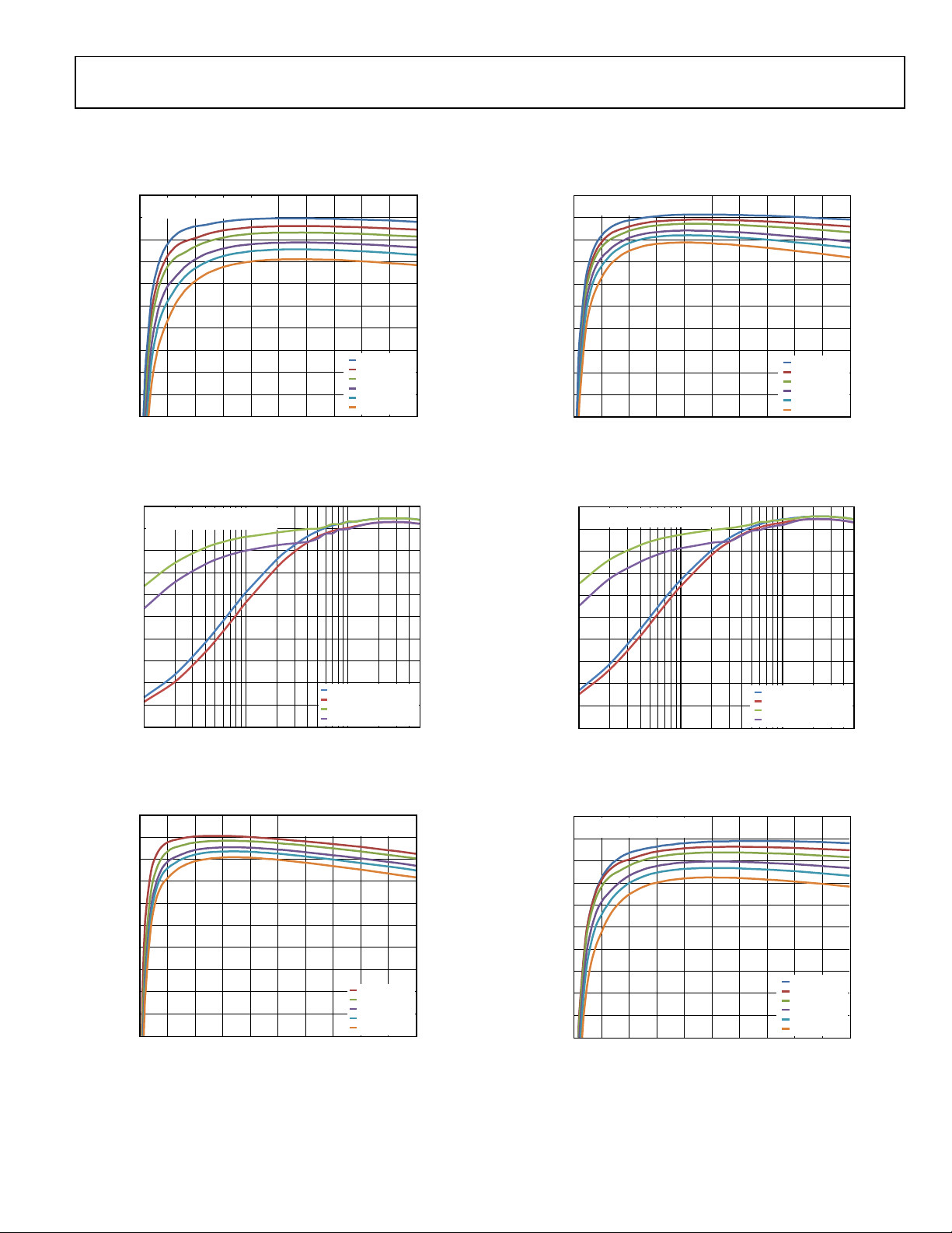
TYPICAL PERFORMANCE CHARACTERISTICS
TA = 25°C, VIN = 12 V, V
Figure 5. Efficiency at V
= 3.3 V, L = 2.2 µH, C
OUT
= 12 V, fSW = 600 kHz, FPWM
IN
= 2 × 100 µF, fSW = 600 kHz, unless otherwise noted.
OUT
Figure 8. Efficiency at VIN = 12 V, fSW = 300 kHz, FPWM
Figure 6. Efficiency at VIN = 12 V, fSW = 600 kHz, FPWM and PFM
Figure 7. Efficiency at VIN = 5 V, fSW = 600 kHz, FPWM
Figure 9. Efficiency at VIN = 12 V, fSW = 300 kHz, FPWM and PFM
Figure 10. Efficiency at VIN = 18 V, fSW = 300 kHz, FPWM
Rev. 0 | Page 9 of 32
Page 10
ADP2325 Data Sheet
10
15
20
25
30
35
40
4 6 8 10 12 14 16 18 20
SHUTDOWN CURRE NT (μA)
T
J
= –40°C
TJ = +25°C
T
J
= +125°C
V
IN
(V)
10036-011
3.5
3.6
3.7
3.8
3.9
4.0
4.1
4.2
4.3
4.4
4.5
–40 –20 0 20 40 60 80 100 120
UVLO THRES HOLD (V)
RISING
FALLING
TEMPERATURE (°C)
10036-012
0.90
0.92
0.94
0.96
0.98
1.00
1.02
1.04
1.06
1.08
1.10
–40 –20 0 20 40 60 80 100 120
EN SOURCE CURRENT ( µA)
TEMPERATURE (°C)
10036-013
2.80
2.85
2.90
2.95
3.00
3.05
3.10
4 6 8 10 12 14 16 18 20
QUIESCENT CURRE NT (mA)
VIN (V)
T
J
= –40°C
T
J
= +25°C
T
J
= +125°C
10036-014
1.00
1.05
1.10
1.15
1.20
1.25
1.30
–40 –20 0 20 40 60 80 100 120
ENABLE THRESHOLD (V)
RISING
FALLING
TEMPERATURE (°C)
10036-015
4.70
4.75
4.80
4.85
4.90
4.95
5.00
5.05
5.10
5.15
5.20
5.25
5.30
–40 –20 0 20 40 60 80 100 120
EN SOURCE CURRENT ( µA)
TEMPERATURE (°C)
10036-016
Figure 11. Shutdown Current vs. VIN
Figure 12. UVLO Threshold vs. Temperature
Figure 14. Quiescent Current vs. VIN
Figure 15. EN Threshold vs. Temperature
Figure 13. EN Source Current vs. Temperature at VEN = 1.5 V
Figure 16. EN Source Current vs. Temperature at VEN = 1 V
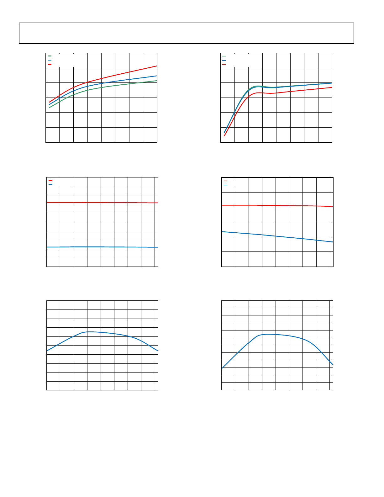
Rev. 0 | Page 10 of 32
Page 11

Data Sheet ADP2325
O
O
604
603
602
601
LTAGE ( mV )
600
599
598
FEEDBACK V
597
596
–40 –20 0 20 40 60 80 100 120
TEMPERATURE ( °C)
Figure 17. Feedback Voltage vs. Temperature
660
R
= 100kΩ
OSC
640
10036-017
600
580
560
540
520
500
480
460
TRANSCONDUC TANCE (µS)
440
420
400
–40 –20 0 20 40 60 80 100 120
TEMPERATURE ( °C)
Figure 20. Transconductance (g
5.4
5.2
) vs. Temperature
m
10036-020
620
600
580
FREQUENCY (kHz)
560
540
–40–200 20406080100120
TEMPERATURE ( °C)
Figure 18. Frequency vs. Temperature
80
75
70
65
60
55
50
45
MOSFET RESISTOR (mΩ)
40
35
30
–40 –20 0 20 40 60 80 100 120
TEMPERATURE ( °C)
Figure 19. MOSFET R
vs. Temperature
DSON
5.0
4.8
LTAG E ( V)
4.6
INTVCC V
4.4
4.2
4.0
4 6 8 101214161820
10036-018
Figure 21. INTVCC Voltage vs. V
4.5
4.3
4.1
3.9
3.7
3.5
3.3
3.1
SSx PIN SO URCE CURRENT ( µA)
2.9
2.7
–40 –20 0 20 40 60 80 100 120
10036-019
VIN (V)
TEMPERATURE (°C)
10036-021
IN
10036-022
Figure 22. SSx Pin Source Current vs. Temperature
Rev. 0 | Page 11 of 32
Page 12

ADP2325 Data Sheet
2
CH1 5V CH2 2V M20ns A CH1 4V
1
T 40.4%
SW
DL
10036-023
6.5
7.0
7.5
8.0
8.5
9.0
9.5
–40 –20 0 20 40 60 80 100 120
PEAK CURRENT LI M IT (A)
TEMPERATURE (°C)
10036-024
CH1 10mV CH2 10V M 1µs A CH2 4.6V
1
4
2
T 42.6%
CH4 2A Ω
B
W
10036-028
V
OUT
(AC)
SW
I
L
CH1 5V CH2 2V M20ns A CH2 4.04V
1
2
T 40.4%
SW
DL
10036-026
TEMPERATURE (°C)
3.5
4.0
4.5
5.0
5.5
6.0
6.5
–40 –20 0 20 40 60 80 100 120
PEAK CURRENT LI M IT (A)
10036-025
CH1 10mV M 1µs A CH2 8.4V
1
4
2
T 47.2%
CH4 1A Ω
B
W
CH2 10V
V
OUT
(AC)
SW
I
L
10036-029
Figure 23. Low-Side Driver Rising Edge Waveform, CDL = 2.2 nF
Figure 24. Peak Current-Limit Threshold vs. Temperature, R
= Floating
ILIM
Figure 26. Low-Side Driver Falling Edge Waveform, CDL = 2.2 nF
Figure 27. Peak Current-Limit Threshold vs. Temperature, R
= 47 kΩ
ILIM
Figure 25. Continuous Conduction Mode (CCM)
Figure 28. Discontinuous Conduction Mode (DCM)
Rev. 0 | Page 12 of 32
Page 13

Data Sheet ADP2325
(AC)
V
OUT
1
1
SW1
I
4
L
SW
2
B
CH1 100mV M 1ms A CH2 8.4V
CH2 10V
W
CH4 1A Ω
T 47.2%
Figure 29. Power Saving Mode
EN
3
V
OUT
1
PGOOD
2
I
OUT
4
B
CH1 2V CH2 5V
CH3 10V
W
CH4 5A Ω
M 1ms A CH3 3.4V
T 20.2%
Figure 30. Soft Start with Full Load
SW2
2
I
L1
4
CH1 10V
10036-032
CH3 2A
B
ΩΩ
W
Figure 32. Dual Phase, Single Output, V
3
1
2
4
10036-030
EN
V
OUT
PGOOD
I
L
B
CH1 2V CH2 5V
CH3 10V
W
CH2 10V
CH4 2A
CH4 2A Ω
I
L2
M 1µs A CH2 5.6V
B
T 50.4%
W
OUT
M 1ms A CH3 3.4V
T 20.2%
= 3.3 V, I
OUT
10036-040
= 10 A
10036-033
Figure 33. Soft Start with Precharged Output
V
(AC)
CH4 2A Ω
OUT
I
OUT
T 20.2%
1
4
CH1 100mV M 200µs A CH4 3.4A
B
W
Figure 31. Load Transient Response, 1 A to 4 A
10036-031
Rev. 0 | Page 13 of 32
V
(AC)
1
3
CH1 20mV M 400µs A CH3 11.5V
CH3 5V
B
W
B
W
Figure 34. Line Transient Response, V
OUT
V
IN
T 73.8%
from 8 V to 14 V, I
IN
OUT
10036-034
= 5 A
Page 14

ADP2325 Data Sheet
CH1 2V M 10ms A CH1 1.32V
1
4
2
T 19.8%
CH4 5A Ω
B
W
CH2 10V
SW
I
L
V
OUT
10036-035
CH3 5V
CH2 10VCH1 10V M 1µs A CH3 2.8V
3
1
2
T 50.4%
SYNC
SW1
SW2
10036-036
CH2 10V
CH3 5V
CH1 10V
M 1µs A CH3 2.8V
1
2
3
T 50.4%
SYNC
SW1
SW2
10036-037
4
M 10ms A CH1 1.32V
T 60.2%
CH4 5A Ω
B
W
CH2 10V
CH1 2V
1
2
SW
I
L
V
OUT
10036-038
CH3 5V
CH2 10VCH1 10V M 1µs A CH3 2.8V
3
1
2
T 50.4%
SYNC
SW1
SW2
10036-039
CH3 5V
CH2 10VCH1 10V M 1µs A CH3 2.5V
3
1
2
T 50.0%
SYNC
SW1
SW2
10036-048
Figure 35. Output Short
Figure 36. External Synchronization with 60° Phase Shift
Figure 38. Output Short Recovery
Figure 39. External Synchronization with 90° Phase Shift
Figure 37. External Synchronization with 120° Phase Shift
Figure 40. SYNC Pin Configured as Output
Rev. 0 | Page 14 of 32
Page 15

Data Sheet ADP2325
CH2 1V M 1ms A CH1 1.56V
2
T 50.4%
B
W
B
W
CH1 1V
V
MASTER
V
SLAVE
10036-057
0
1
2
3
4
5
6
25 40 55 70 85 100
OUTPUT CURRE NT OF CH2 (A)
AMBIENT TEMPERATURE (°C)
CH1 = 0A
CH1 = 1A
CH1 = 2A
CH1 = 3A
CH1 = 4A
CH1 = 5A
V
OUT1
= 1.2V
V
OUT2
= 3.3V
f
SW
= 500kHz
10036-058
CH2 1V M 1ms A CH1 1.58V
2
T 49.8%
B
W
B
W
CH1 1V
V
MASTER
V
SLAVE
10036-059
0
1
2
3
4
5
6
OUTPUT CURRENT OF CH1 (A)
25 40 55 70 85 100
AMBIENT TEMPERATURE (°C)
V
OUT1
= 1.2V
V
OUT2
= 3.3V
f
SW
= 500kHz
10036-060
CH2 = 0A
CH2 = 1A
CH2 = 2A
CH2 = 3A
CH2 = 4A
CH2 = 5A
Figure 41. Coincident Tracking
Figure 42. Thermal Derating Performance at 110°C Case Temperature Based
on ADP2325-EVALZ Board
Figure 43. Ratiometric Tracking
Figure 44. Thermal Derating Performance at 110°C Case Temperature Based
on ADP2325-EVALZ Board
Rev. 0 | Page 15 of 32
Page 16

ADP2325 Data Sheet
V
THEORY OF OPERATION
The ADP2325 is a full featured, dual output, step-down dc-to-dc
regulator based on a current mode architecture. It integrates two
high-side power MOSFETs and two low-side drivers for external
MOSFETs. The ADP2325 is designed for high performance
applications that require high efficiency and design flexibility.
The ADP2325 can operate with an input voltage from 4.5 V
to 20 V and can regulate the output voltage to as low as 0.6 V.
Additional features for flexible design include programmable
switching frequency, programmable soft start, external compensation, independent enable inputs, and power-good outputs.
CONTROL SCHEME
The ADP2325 uses a fixed frequency, current mode PWM control
architecture during medium to full loads, but shifts to a power
save mode (PFM) at light loads when the PFM mode is enabled.
The power save mode reduces switching losses and boosts efficiency under light loads.
When operating in the fixed frequency PWM mode, the duty
cycle of the integrated N-channel MOSFET (referred to interchangeably as NFET or MOSFET) is adjusted, this, in turn,
regulates the output voltage. When the device operates in
power save mode, the switching frequency is adjusted to regu
late the output voltage.
PWM MODE
In PWM mode, the ADP2325 operates at a fixed frequency
set by an external resistor. At the start of each oscillator cycle, the
high-side NFET turns on, placing a positive voltage across the
inductor. The inductor current increases until the current sense
signal crosses the peak inductor current threshold, turning off the
high-side NFET and turning on the low-side NFET (diode). This
places a negative voltage across the inductor, causing a reduction in
the inductor current. The low-side NFET (diode) stays on for the
remainder of the cycle or until the inductor current reaches zero.
PFM MODE
To enable the PFM mode, pull the MODE pin to ground. When
the COMPx voltage is below the PFM threshold voltage, the
device enters the PFM mode.
When the device enters the PFM mode, it monitors the FBx voltage
to regulate the output voltage. Because the high-side and lowside NFETs are turned off, the load current discharges the output
capacitor causing the output voltage to drop. When the FBx
voltage drops below 0.605 V, the device starts switching and the
output voltage increases as the output capacitor is charged by the
inductor current. When the FBx voltage exceeds 0.62 V, the device
turns off both the high-side and low-side NFETs until the FBx
voltage drops to 0.605 V. In the PFM mode, the output voltage
ripple is larger than the ripple in the PWM mode.
PRECISION ENABLE/SHUTDOWN
The ADP2325 has two independent enable pins (EN1 and
EN2), one for each channel. The ENx pin has an internal pulldown current source of 5 μA to provide a default turn-off whenever
an ENx pin is open.
When the voltage on the EN1 or EN2 pin exceeds 1.2 V (typical),
Channel 1 (per the EN1 pin) or Channel 2 (per the EN2 pin) is
enabled and the internal pull-down current source at the EN1
or EN2 pin is reduced to 1 μA, which allows the user to program
the UVLO lockout of the input voltage.
When the voltage on the EN1 or EN2 pin drops below 1.1 V
(typical), Channel 1 or Channel 2 turns off. When EN1 and
EN2 are both below 1.1 V, all of the internal circuits turn off
and the device enters the shutdown mode.
SEPARATE INPUT VOLTAGES
The ADP2325 supports two separate input voltages. This means
that the PVIN1 and PVIN2 voltages can be connected to two
different supply voltages. In these types of applications, because
the PVIN1 voltage provides the power supply for the internal regulator and control circuitry, the PVIN1 voltage must be above the
UVLO voltage before the PVIN2 voltage begins to rise.
This feature allows for a cascading supply operation, as shown in
Figure 45 where PVIN2 is sourced from the Channel 1 output.
In this configuration, the Channel 1 output voltage needs to be high
enough to maintain Channel 2 in regulation, and the Channel 1
output voltage must be higher than the input voltage UVLO
threshold.
OUT1
C
OUT1
V
IN
L1
M1
PVIN1
SW1
DL1
Figure 45. Cascading Supply Operation
ADP2325
PGND
PVIN2
SW2
DL2
M2
L2
C
V
OUT2
OUT2
INTERNAL REGULATOR (INTVCC)
The internal regulator provides a stable voltage supply for the
internal control circuits and a bias voltage for the low-side gate
drivers. It is recommended that a 1 μF ceramic capacitor be placed
between INTVCC and GND. The internal regulator also includes a
current-limit circuit for protection.
The internal regulator is active when either of the channels is
enabled. The PVIN1 pin provides power for the internal regulator,
which is used by both channels.
10036-041
Rev. 0 | Page 16 of 32
Page 17

Data Sheet ADP2325
C
BOOTSTRAP CIRCUITRY
The ADP2325 integrates the boot regulators to provide the gate
drive voltage for the high-side NFETs. The regulators generate
5 V bootstrap voltages between the BSTx and the SWx pins.
It is recommended that an X7R or X5R, 0.1 µF ceramic
capacitor be placed between the BSTx and the SWx pins.
LOW-SIDE DRIVER
The DLx pin provides the gate drive for the low-side N-channel
MOSFET. Internal circuitry monitors the gate driver signal to
ensure break-before-make switching to prevent crossconduction.
The VDRV pin provides the power supply to the low-side drivers.
It is limited to a 5.5 V maximum input; placing a 1 µF ceramic
capacitor close to this pin is recommended.
OSCILLATOR
A resistor from RT to GND programs the switching frequency
according to the following equation:
00060
f
[kHz] =
SW
,
OSC
]k[
R
A 200 kΩ resistor sets the frequency to 300 kHz, and a 100 kΩ
resistor sets the frequency to 600 kHz. Figure 46 shows the
typical relationship between f
1200
1100
1000
900
Y (kHz)
800
700
600
500
SWITCHING FREQUEN
400
300
200
70 110 150 190 230 250
50 90 130 170 210
Figure 46. f
SW
R
OSC
and R
(kΩ)
vs. R
SW
OSC
OSC
.
10036-042
SYNCHRONIZATION
The SYNC pin can be configured as an input or an output by
setting the SCFG pin, as shown in Table 5.
Table 5. SCFG Configuration
SCFG SYNC Phase Shift
INTVCC Output 0°
GND Input 90°
180 kΩ to GND Input 120°
100 kΩ to GND Input 60°
When the SYNC pin is configured as an output, it generates a
clock with a frequency that is equal to the internal switching
frequency.
When the SYNC pin is configured as an input, the ADP2325 synchronizes to the external clock that is applied to the SYNC pin, and
the internal clock must be programmed lower than the external
clock. The phase shift can be programmed by the SCFG pin.
When working in synchronization mode, the ADP2325 disables
the PFM mode and works only in the CCM mode.
SOFT START
Use the SSx pins to program the soft start time. Place a capacitor
between SSx and GND; an internal current charges this capacitor
to establish the soft start ramp. The soft start time can be calculated
using the following equation:
C
V6.0
t
SS
SS
I
SS
where:
C
is the soft start capacitance.
SS
is the soft start pull-up current (3.5 µA).
I
SS
If the output voltage is precharged prior to power-up, the ADP2325
prevents the low-side MOSFET from turning on until the soft
start voltage exceeds the voltage on the FBx pin.
During soft start, the ADP2325 uses frequency foldback to
prevent output current runaway. The switching frequency is
reduced according to the voltage present at the FBx pin, which
allows more time for the inductor to discharge. The correlation
between the switching frequency and the FBx pin voltage is listed
in Table 6.
Table 6. FBx Pin Voltage and Switching Frequency
FBx Pin Voltage Switching Frequency
VFB ≥ 0.4 V fSW
0.4 V > VFB ≥ 0.2 V 1/2 fSW
VFB < 0.2 V 1/4 fSW
PEAK CURRENT-LIMIT AND SHORT-CIRCUIT PROTECTION
The ADP2325 uses a peak current-limit protection circuit to
prevent current runaway. Place a resistor between DLx and PGND
to program the peak current-limit value, as listed in Table 7.
The programmable peak current-limit threshold feature allows
for the use of a small size inductor for low current applications.
Table 7. Peak Current-Limit Threshold Setting
R
Peak Current-Limit Threshold
ILIM
Floating 8 A
47 kΩ 4.8 A
The ADP2325 uses hiccup mode for overcurrent protection.
When the peak inductor current reaches the current-limit
threshold, the high-side MOSFET turns off and the low-side
driver turns on until the next cycle while the overcurrent counter
is incremented.
Rev. 0 | Page 17 of 32
Page 18

ADP2325 Data Sheet
BOTTRK
TOPTRK
BOT
TOP
MASTER
SLAVE
R
R
R
R
V
V
_
_
11+
+
=
FBx
TRKx SWx
ADP2325
V
MASTER
R
TRK_TOP
R
TRK_BOT
V
SLAVE
R
TOP
R
BOT
10036-043
TIME
VOLTAGE
V
MASTER
V
SLAVE
10036-044
TIME
VOLTAGE
V
MASTER
V
SLAVE
10036-045
If the overcurrent counter reaches 10, or if the FBx pin voltage
falls to 0.2 V after the soft start, the device enters hiccup mode.
During this mode, the high-side MOSFET and low-side driver are
both turned off. The device remains in this mode for seven soft
start cycles and then attempts to restart from soft start. If the
current-limit fault is cleared, the device resumes normal
operation; otherwise, it reenters hiccup mode.
The ADP2325 provides a negative current limit. When the low-side
FET voltage exceeds the negative current-limit threshold voltage
(50 mV typical), the low-side FET turns off immediately for the
remainder of this cycle. Both the high-side and low-side FETs
turn off until the next cycle.
In some cases, the input voltage (PVIN) ramp rate is too slow
or the output capacitor is too large to support the set regulation
voltage during the soft start, causing the device to enter the
hiccup mode. To prevent such cases, use a resistor divider at the
ENx pin to program the UVLO of the input voltage or use a
longer soft start time.
VOLTAGE TRACKING
The ADP2325 has a tracking input, TRKx, that allows the output
voltage to track an external (master) voltage. Voltage tracking
allows power sequencing applicable for FPGAs, DSPs, and ASICs,
which may require a power sequence between the core and the I/O
voltages.
The internal error amplifier includes three positive inputs: the
internal reference voltage, the soft start voltage, and the tracking
input voltage. The error amplifier regulates the feedback voltage
to the lowest of the three voltages. To track a master voltage,
connect the TRKx pin to a resistor divider from the master
voltage, as shown in Figure 47.
Coincident Tracking
A common application is coincident tracking, which is shown in
Figure 48. Coincident tracking limits the slave output voltage to
be the same as the master voltage until it reaches regulation. To
enable coincident tracking, set R
Figure 48. Coincident Tracking
TRK_TOP
= R
TOP
and R
TRK_BOT
= R
BOT
Ratiometric Tracking
In ratiometric tracking, the slave output voltage is limited to a fraction of the master voltage. In this application, the slave and master
voltages reach their final values at the same time (see Figure 49).
Figure 49. Ratiometric Tracking
The ratio of the slave output voltage to the master voltage is a
function of the two dividers, as follows:
.
Figure 47. Voltage Tracking
The final TRKx pin voltage must be higher than 0.54 V. If the
tracking function is not used, connect the TRKx pin to INTVCC.
PARALLEL OPERATION
The ADP2325 supports a 2-phase parallel operation to provide
a single output of 10 A. To configure the ADP2325 as a 2-phase
single output
1. Connect the FB2 pin to INTVCC, thereby disabling the
Channel 2 error amplifier.
2. Connect COMP1 to COMP2 and connect EN1 to EN2.
3. Use SS1 to set the soft start time and keep SS2 open.
During parallel operation, the voltages of PVIN1 and PVIN2
should be the same.
Rev. 0 | Page 18 of 32
Page 19

Data Sheet ADP2325
POWER GOOD
The power-good (PGOODx) pin is an active high, open-drain
output that indicates whether the regulator output voltage is
within regulation. Logic high indicates that the voltage at the
FBx pin (and, therefore, the output voltage) is above 90% of the
reference voltage. Logic low indicates that the voltage at the FBx
pin (and, therefore, the output voltage) is below 85% of the
reference voltage. There is a 16-cycle deglitch time between FBx
and PGOODx.
OVERVOLTAGE PROTECTION
The ADP2325 provides an OVP feature to protect the system
against an output shorting to a higher voltage supply or for
when a strong load transient occurs. If the feedback voltage
increases to 0.7 V, the internal high-side MOSFET and low-side
driver turn off until the voltage at the FBx pin is reduced to
0.63 V, at which time the ADP2325 resumes normal operation.
UNDERVOLTAGE LOCKOUT
The UVLO threshold is 4.2 V with 0.5 V hysteresis to prevent
power-on glitches on the device. When the PVIN1 or PVIN2
voltage rises above 4.2 V, Channel 1 or Channel 2 is enabled and the
soft start period initiates. When either PVIN1 or PVIN2 drops
below 3.7 V, it turns off Channel 1 or Channel 2, respectively.
THERMAL SHUTDOWN
In the event that the ADP2325 junction temperature exceeds
150°C, the thermal shutdown circuit turns off the regulator. A
15°C hysteresis is included so that the ADP2325 does not recover
from thermal shutdown until the on-chip temperature drops
below 135°C. Upon recovery, soft start initiates prior to normal
operation.
Rev. 0 | Page 19 of 32
Page 20

ADP2325 Data Sheet
( )
DDII
OUT
_rms
IN
C
−××= 1
+×=
BOT
TOP
OUT
R
R
V 16.0
5.0
22
3
( )
SW
L
OUT
IN
fI
DVV
L
×
∆
×−
=
IN
OUT
V
V
D =
APPLICATIONS INFORMATION
INPUT CAPACITOR SELECTION
The input decoupling capacitor attenuates high frequency noise
on the input and acts as an energy reservoir. This capacitor should
be a ceramic capacitor in the range of 10 µF to 47 µF and must
be placed close to the PVINx pin. The loop composed of this
input capacitor, high-side NFET, and low-side NFET must be
kept as small as possible. The voltage rating of the input capacitor
must be greater than the maximum input voltage. Ensure that the
rms current rating of the input capacitor is larger than that
expressed in following equation:
OUTPUT VOLTAGE SETTING
The output voltage of the ADP2325 can be set by an external
resistor divider using the following equation:
To limit output voltage accuracy degradation due to FBx pin
bias current (0.1 µA maximum) to less than 0.5% (maximum),
ensure that R
is less than 30 kΩ. Table 8 provides the recom-
BOT
mended resistor divider for various output voltage options.
Table 8. Resistor Divider for Various Output Voltages
V
(V) R
OUT
, ±1% (kΩ) R
TOP
, ±1% (kΩ)
BOT
1.0 10 15
1.2 10 10
1.5 15 10
1.8 20 10
2.5 47.5 15
3.3 10 2.21
VOLTAGE CONVERSION LIMITATIONS
The minimum output voltage for a given input voltage and
switching frequency is limited by the minimum on time. The
minimum on time of the ADP2325 is typically 130 ns. The
minimum output voltage in CCM mode at a given input voltage
and frequency can be calculated using the following equation:
V
= VIN × t
OUT_MIN
t
× fSW − (R
MIN_ON
where:
V
t
I
f
R
R
R
is the minimum output voltage.
OUT_MIN
is the minimum on time.
MIN_ON
is the minimum output current.
OUT_MIN
is the switching frequency.
SW
is the high-side MOSFET on resistance.
DSON1
is the low-side MOSFET on resistance.
DSON2
is the series resistance of the output inductor.
L
MIN_ON
DSON2
× fSW − (R
+ RL) × I
DSON1
OUT_MIN
− R
DSON2
) × I
OUT_MIN
×
The maximum output voltage for a given input voltage and
switching frequency is also limited by the minimum off time
and the maximum duty cycle. The minimum off time is typically
150 ns and the maximum duty is typically 90% in the ADP2325.
The maximum output voltage that is limited by the minimum off
time at a given input voltage and frequency can be calculated
using the following equation:
V
I
OUT_MAX
OUT_MAX
= VIN × (1 − t
× (1 − t
MIN_OFF
× fSW) − (R
MIN_OFF
× fSW) − (R
DSON2
− R
DSON1
+ RL) × I
DSON2
OUT_MAX
) ×
where:
V
t
I
is the maximum output voltage.
OUT_ MAX
is the minimum off time.
MIN_OFF
is the maximum output current.
OUT_ MAX
The maximum output voltage that is limited by the maximum
duty cycle at a given input voltage can be calculated using the
following equation:
V
where D
= D
OUT_MAX
is the maximum duty cycle.
MAX
MAX
× VIN
As the previous equations demonstrate, reducing the switching
frequency alleviates the minimum on time and minimum off time
limitation.
CURRENT-LIMIT SETTING
The ADP2325 has two selectable current-limit thresholds. Make
sure that the selected current-limit value is larger than the peak
current of the inductor, I
PEAK
.
INDUCTOR SELECTION
The inductor value is determined by the operating frequency,
input voltage, output voltage, and inductor ripple current. Using
a small inductor provides faster transient response but degrades
efficiency due to larger inductor ripple current, whereas a large
inductor value provides smaller ripple current and better efficiency but results in a slower transient response. Thus, there is a
trade-off between the transient response and efficiency. As a
guideline, the inductor ripple current, ΔI
one-third of the maximum load current. The inductor value can
be calculated by using the following equation:
where:
V
is the input voltage.
IN
V
is the output voltage.
OUT
ΔI
is the inductor ripple current.
L
f
is the switching frequency.
SW
D is the duty cycle.
, is typically set to
L
Rev. 0 | Page 20 of 32
Page 21

Data Sheet ADP2325
I
The ADP2325 uses adaptive slope compensation in the current
loop to prevent subharmonic oscillations when the duty cycle is
larger than 50%. The internal slope compensation limits the minimum inductor value.
For a duty cycle that is larger than 50%, the minimum inductor
value is determined by the following equation:
1
OUT
fDV2
SW
The inductor peak current is calculated by
III
L
OUT
2
PEAK
The saturation current of the inductor must be larger than the
peak inductor current. For the ferrite core inductors with a
quick saturation characteristic, the saturation current rating of the
inductor should be higher than the current-limit threshold of the
switch to prevent the inductor from entering saturation.
The rms current of the inductor can be calculated by
2
III
2
L
RMS
OUT
12
Shielded ferrite core materials are recommended for low core
loss and low EMI.
Table 9. Recommended Inductors
Vendor Part No.
Sumida CDRH105RNP-0R8N 0.8 13.5 9.5 4.3
CDRH105RNP-1R5N 1.5 10.5 8.3 5.8
CDRH105RNP-2R2N 2.2 9.25 7.5 7.2
CDRH105RNP-3R3N 3.3 7.8 6.5 10.4
CDRH105RNP-4R7N 4.7 6.4 6.1 12.3
CDRH105RNP-6R8N 6.8 5.4 5.4 18
Coilcraft MSS1048-152NL 1.5 10.5 10.8 5.1
MSS1048-222NL 2.2 8.4 9.78 7.2
MSS1048-332NL 3.3 7.38 7.22 10.1
MSS1048-472NL 4.7 6.46 6.9 11.4
MSS1048-682NL 6.8 5.94 6.01 15.4
Wurth
Elektronik
7447797110 1.1 16 7.6 14
7447797180 1.8 13.3 7.3 16
7447797300 3.0 10.5 7.0 18
7447797470 4.7 8.0 5.8 27
7447797620 6.2 7.5 5.5 30
Value
(μH)
I
SAT
(A)
I
DCR
RMS
(A)
(mΩ)
OUTPUT CAPACITOR SELECTION
The output capacitor selection affects both the output voltage
ripple and the loop dynamics of the regulator. For example,
during load step transient on the output, when the load is suddenly increased, the output capacitor supplies the load until the
control loop can ramp up the inductor current, which causes an
undershoot of the output voltage. Use the following equation to
calculate the output capacitance that is required to meet the voltage
droop requirement:
2
LIK
STEP
STEP
_
I
L
Vf
VVV
OUT_UVOUT
2
LIK
2
OUT_RIPPLE
2
VVV
OUTOVOUTOUT
OUT_UV
, C
OUT_OV
,
C
OUT_UV
UV
2
IN
where:
I
is the load step.
Δ
STEP
Δ
V
is the allowable undershoot on the output voltage.
OUT_UV
K
is a factor, typically setting KUV = 2.
UV
Another example is when a load is suddenly removed from the
output and the energy stored in the inductor rushes into the
output capacitor, which causes the output to overshoot. The
output capacitance required to meet the overshoot requirement
can be calculated using the following equation:
C
OUT_OV
OV
where:
V
Δ
K
is the allowable overshoot on the output voltage.
OUT_OV
is a factor, typically setting KOV = 2.
OV
The output ripple is determined by the ESR of the output
capacitor and its capacitance value. Use the following equation to
select a capacitor that can meet the output ripple requirements:
8
V
OUT_RIPPLE
I
L
SW
C
OUT_RIPPLE
R
ESR
where:
V
Δ
R
ESR
OUT_RIPPLE
is the allowable output voltage ripple.
is the equivalent series resistance of the output capacitor.
Select the largest output capacitance given by C
and C
OUT_RIPPLE
to meet both load transient and output ripple
performance.
The selected output capacitor voltage rating must be greater
than the output voltage. The minimum rms current rating of
the output capacitor is determined by the following equation:
I
OUT
_LrmsC
12
Rev. 0 | Page 21 of 32
Page 22

ADP2325 Data Sheet
Fairchild
FDS8880
30 V
10.7 A
12 mΩ
12 nC
μA1V2.1μA5V1.1
V2.1V1.1
×−×
×−×
=
IN_FALLINGIN_RISING
TOP_EN
VV
R
V2.1μ5
V2.1
_
_
_
_
−Α×−
×
=
ENTOP
RISINGIN
ENTOP
ENBOT
RV
R
R
××
+
××
+
××==
P
Z
VI
COMP
OUT
VD
f
s
f
s
RA
sV
sV
sG
π
π
2
1
2
1
)(
)(
)(
OUT
ESR
Z
CRf×××
=
π
2
1
( )
OUT
ESR
P
CRR
f
×+××
=
π
2
1
ENx
1.2V
EN CMP
4µA1µA
PVINx
R
TOP_EN
R
BOT_EN
10036-046
LOW-SIDE POWER DEVICE SELECTION
The ADP2325 has integrated low-side MOSFET drivers, which
can drive the low-side N-channel MOSFETs (NFETs). The selection of the low-side N-channel MOSFET affects the dc-to-dc
regulator performance.
The selected MOSFET must meet the following requirements:
PROGRAMMING THE UVLO INPUT
The precision enable input can be used to program the UVLO
threshold and hysteresis of the input voltage, as shown in Figure 50.
• Drain source voltage (V
• Drain current (I
I
LIMIT_MAX
) must be greater than 1.2 × I
D
is the selected maximum current-limit threshold.
) must be higher than 1.2 × VIN.
DS
LIMIT_MAX
, where
The ADP2325 low-side gate drive voltage is 5 V. Make sure that
the selected MOSFET can be fully turned on at 5 V.
Total gate charge (Qg at 5 V) must be less than 50 nC. Lower Qg
characteristics constitute higher efficiency.
When the high-side MOSFET is turned off, the low-side MOSFET
carries the inductor current. For low duty cycle applications, the
low-side MOSFET carries the current for most of the period. To
achieve higher efficiency, it is important to select a low on-resistance MOSFET. The power conduction loss for the low-side
MOSFET can be calculated by
P
where R
FET_LOW
DSON
2
= I
× R
OUT
× (1 − D)
DSON
is the on resistance of the low-side MOSFET.
Make sure that the MOSFET can handle the thermal dissipation
due to the power loss.
In some cases, efficiency is not critical for the system; therefore,
the diode can be selected as the low-side power device. The
average current of the diode can be calculated by
I
DIODE (AVG)
= (1 − D) × I
OUT
The reverse breakdown voltage rating of the diode must be
greater than the input voltage with an appropriate margin to
allow for ringing, which may be present at the SWx node. A
Schottky diode is recommended because it has a low forward
voltage drop and a fast switching speed.
If a diode is used for the low-side device, the ADP2325 must
enable the PFM mode by connecting the MODE pin to ground.
and R
BOT_EN
:
Figure 50. Programming the UVLO Input
Use the following equation to calculate R
TOP_EN
where:
V
V
is the VIN rising threshold.
IN_RISING
is the VIN falling threshold.
IN_FALLING
COMPENSATION COMPONENTS DESIGN
In peak current mode control, the power stage can be simplified
to a voltage controlled current source supplying current to the
output capacitor and load resistor. It is composed of one domain
pole and a zero contributed by the output capacitor ESR. The
control-to-output transfer function is shown in the following
equations:
Table 10. Recommended MOSFETs
Vendor Part No. VDS ID
R
DSON
Fairchild FDMS7578 25 V 14 A 8 mΩ 8 nC
Fairchild FDS6898A 20 V 9.4 A 14 mΩ 16 nC
Vishay Si4804CDY 30 V 7.9 A 27 mΩ 7 nC
Vishay SiA430DJ 20 V 10.8 A 18.5 mΩ 5.3 nC
AOS AON7402 30 V 39 A 15 mΩ 7.1 nC
AOS AO4884L 40 V 10 A 16 mΩ 13.6 nC
Qg
Rev. 0 | Page 22 of 32
where:
A
= 8.33 A/V.
VI
R is the load resistance.
C
is the output capacitance.
OUT
R
is the equivalent series resistance of the output capacitor.
ESR
Page 23

Data Sheet ADP2325
(s)G
s
CC
CCR
s
sCR
CC
g
RR
R
(s)T
VD
CPC
CPCC
CC
CPC
m
TOPBOT
BOT
V
×
×
+
××
+×
××+
×
+
−
×
+
=
1
1
VI
m
C
OUTOUT
C
Ag
fCV
R
××
××××
=
V6.0
2
π
( )
C
OUT
ESR
C
R
CRR
C×+=
C
OUT
ESR
CP
R
CRC×
=
R
ESR
R
+
–
g
m
R
C
C
CP
C
OUT
C
C
R
TOP
R
BOT
–
+
A
VI
V
OUT
V
COMP
V
OUT
10036-047
The ADP2325 uses a transconductance amplifier for the error
amplifier to compensate the system. Figure 51 shows the
simplified peak current mode control small signal circuit.
The following design guidelines show how to select the compensation components, R
, CC, and CCP, for ceramic output capacitor
C
applications.
4. Determine the cross frequency (f
between f
5. R
can be calculated by using the following equation:
C
/12 and fSW/6.
SW
). Generally, the fC is
C
Figure 51. Simplified Peak Current Mode Control Small Signal Circuit
The compensation components, RC and CC, contribute a zero,
and the optional C
and RC contribute an optional pole.
CP
The closed-loop transfer equation is as follows:
6. Place the compensation zero at the domain pole (f
C
can be determined by
C
).
P
7. C
is optional. It can be used to cancel the zero caused by
CP
the ESR of the output capacitor.
The ADP2325 has an internal 10 pF capacitor at the COMPx
pin; therefore, if C
is smaller than 10 pF, no external capacitor
CP
is required.
Rev. 0 | Page 23 of 32
Page 24

ADP2325 Data Sheet
Output Current
I
= 5 A
−×=6.0
6.0
OUT
TOPBOT
V
RR
( )
( )
kHz
000,60
kΩ
SW
OSC
f
R =
( )
SW
L
OUT
IN
fI
DVV
L
×∆
×−
=
( )
SW
OUT
IN
L
fL
DVV
I
×
×−
=∆
2
L
OUT
PEAK
III∆
+=
12
2
2
L
OUT
RMS
III∆
+=
RIPPLEOUT
SW
L
OUT_RIPPLE
Vf
I
C
_
8 ∆××
∆
=
L
RIPPLEOUT
ESR
I
V
R
_
∆
=
DESIGN EXAMPLE
This section describes the design procedure and component
selection for the example application shown in Figure 54, and
Table 11 provides a list of the required settings.
Calculate the peak-to-peak inductor ripple current as follows:
Table 11. Dual Step-Down DC-to-DC Regulator Requirements
Parameter Specification
Channel 1
Input Voltage V
Output Voltage V
Output Voltage Ripple ΔV
= 12.0 V ± 10%
IN1
= 1.2 V
OUT1
OUT1
OUT1_RIPPLE
= 12 mV
Load Transient ±5%, 1 A to 4 A, 1 A/µs
Channel 2
Input Voltage V
Output Voltage V
Output Current I
Output Voltage Ripple ΔV
= 12.0 V ± 10%
IN2
= 3.3 V
OUT2
= 5 A
OUT2
OUT2_RIPPLE
= 33 mV
Load Transient ±5%, 1 A to 4 A, 1 A/µs
Switching Frequency fSW = 500 kHz
OUTPUT VOLTAGE SETTING
Choose a 10 kΩ top feedback resistor (R
bottom feedback resistor using the following equation:
To set the output voltage to 1.2 V, the resistor values are R
10 kΩ and R
the resistors values are R
= 10 kΩ. To set the output voltage to 3.3 V,
BOT1
= 10 kΩ and R
TOP2
TOP
); calculate the
= 2.21 kΩ.
BOT2
TOP1
=
CURRENT-LIMIT SETTING
For 5 A output current operation, the typical peak current
limit is 8 A. In this case, no R
is required.
ILIM
FREQUENCY SETTING
To set the switching frequency to 500 kHz, use the following
equation to calculate the resistor value, R
OSC
:
For V
= 1.2 V, ΔIL1 = 1.44 A. For V
OUT1
= 3.3 V, ΔIL2 = 1.45 A.
OUT2
Find the peak inductor current using the following equation:
For the 1.2 V rail, the peak inductor current is 5.73 A, and for
the 3.3 V rail, the peak inductor current is 5.73 A.
The rms current through the inductor can be estimated by
The rms current of the inductor for both the 1.2 V and 3.3 V
rails is approximately 5.02 A.
For the 1.2 V rail, select an inductor with a minimum rms
current rating of 5.01 A and a minimum saturation current
rating of 5.73 A. For the 3.3 V rail, select an inductor with a
minimum rms current rating of 5.02 A and a minimum
saturation current rating of 5.73 A.
Based on these requirements, for the 1.2 V rail, select a
1.5 µH inductor, such as the Sumida CDRH105RNP-1R5N,
with a DCR = 5.8 mΩ; for the 3.3 V rail, select a 3.3 µH
inductor, such as the Sumida CDRH105RNP-3R3N, with a
DCR = 10.4 mΩ.
OUTPUT CAPACITOR SELECTION
The output capacitor is required to meet the output voltage
ripple and load transient requirements. To meet the output
voltage ripple requirement, use the following equation to
calculate the capacitance and ESR:
Therefore, R
=120 kΩ.
OSC
INDUCTOR SELECTION
The peak-to-peak inductor ripple current, ΔIL, is set to 30%
of the maximum output current. Use the following equation
to estimate the value of the inductor:
For V
Inductor L2 = 3.2 µH.
Select the standard inductor value of 1.5 µH and 3.3 µH for
the 1.2 V and 3.3 V rails.
= 1.2 V, Inductor L1 = 1.4 µH, and for V
OUT1
OUT2
= 3.3 V,
Rev. 0 | Page 24 of 32
For V
V
OUT2
= 1.2 V, C
OUT1
= 3.3 V, C
OUT_RIPPLE1
OUT_RIPPLE2
= 30 µF and R
= 11 µF and R
ESR1
= 23 mΩ.
ESR2
= 8.3 mΩ. For
Page 25

Data Sheet ADP2325
( )
2
2
_
2
OUTOVOUTOUT
STEP
OV
OUT_OV
VVV
LIK
C
−∆+
×∆×
=
( )
UVOUTOUT
IN
STEP
UV
OUT_UV
VVV
LIK
C
_
2
2 ∆×−×
×∆×
=
kΩ9.28
A/V8.33μS500V0.6
kHz50
μF643V2.12
=
××
×××××
=
π
C1
R
( )
pF1598
kΩ9.28
μF643Ω001.0Ω24.0
=
××+
=
C1
C
pF6.6
kΩ9.28
μF643Ω001.0
=
××
=
CP1
C
kΩ5.26
A/V8.33μS500V0.6
kHz50μF232V3.32
=
××
×××××
=
π
C2
R
( )
pF1594
kΩ
5.26
μF322Ω001.0Ω66.0
=
××+
=
C2
C
pF4.2
kΩ
5.26
μF322Ω001.0
=
××
=
CP2
C
1k
–60
60
–48
48
–36
–24
–12
12
24
36
MAGNITUDE ( dB)
PHASE (Degrees)
FREQUENCY (Hz)
0
–180
180
–144
144
–108
–72
–36
36
72
108
0
10k 100k
1 2
1M
10036-061
1k
–60
60
–48
48
–36
–24
–12
12
24
36
MAGNITUDE ( dB)
PHASE (Degrees)
FREQUENCY (Hz)
0
–180
180
–144
144
–108
–72
–36
36
72
108
0
10k 100k
1 2
1M
10036-062
To meet the ±5% overshoot and undershoot requirement, use
the following equation to calculate the capacitance:
Figure 52 shows the 1.2 V rail bode plot at 5 A. The cross
frequency is 42 kHz and the phase margin is 50°.
For estimation purposes, use K
use C
use C
= 188 µF and C
OUT_OV1
= 55 µF and C
OUT_OV2
OUT_UV2
= KUV = 2. For V
OV
= 21 µF. For V
OUT_UV1
= 21 µF.
OUT1
OUT2
= 1.2 V,
= 3.3 V,
For the 1.2 V rail, ESR of the output capacitor must be smaller
than 8.3 mΩ, and the output capacitance must be larger than
188 µF. It is recommend that three 100 µF, X5R, 6.3 V ceramic
capacitors be used, such as the GRM32ER60J107ME20 from
Murata, with an ESR = 2 mΩ.
For the 3.3 V rail, the ESR of the output capacitor must be
smaller than 23 mΩ, and the output capacitance must be
larger than 55 µF. It is recommended that two 47 µF, X5R,
6.3 V ceramic capacitors be used, such as the Murata
GRM32ER60J476ME20, with an ESR = 2 mΩ.
LOW-SIDE MOSFET SELECTION
A low R
solutions. The MOSFET breakdown voltage must be greater
than 1.2 V × V
1.2 V × I
It is recommended that a 30 V, N-channel MOSFET be used, such
as the FDS8880 from Fairchild. The R
4.5 V driver voltage is 12 mΩ, and the total gate charge is 12 nC.
N-channel MOSFET is selected for high efficiency
DSON
, and the drain current must be greater than
IN
.
LIMIT
of the FDS8880 at a
DSON
COMPENSATION COMPONENTS
For better load transient and stability performance, set the
cross frequency, f
therefore, the f
For the 1.2 V rail, the 100 µF ceramic output capacitor has
a derated value of 64 µF.
, to fSW/10. In this case, fSW runs at 500 kHz;
C
is set to 50 kHz.
C
Figure 52. Bode Plot for 1.2 V Rail
For the 3.3 V rail, the 47 µF ceramic output capacitor has a
derated value of 32 µF.
By using standard component values of R
C
= 1500 pF, no C
C2
is needed.
CP2
= 27 kΩ and
C2
Figure 53 shows the 3.3 V rail bode plot at 5 A. The cross
frequency is 55 kHz and phase margin is 67°.
By choosing standard components where R
1500 pF, no C
is needed.
CP1
= 28 kΩ and CC1 =
C1
Figure 53. Bode Plot for 3.3 V Rail
Rev. 0 | Page 25 of 32
Page 26

ADP2325 Data Sheet
nF5.17
V6.0
ms3μA5.3
V6.0
=
×
=
×
=
SSSS
SS
tI
C
SOFT START TIME PROGRAMMING
The soft start feature allows the output voltage to ramp up in
a controlled manner, eliminating output voltage overshoot
during soft start and limiting inrush current. The soft start
time is set to 3 ms.
= C
Choose a standard component value of C
SS1
= 22 nF.
SS2
INPUT CAPACITOR SELECTION
A minimum 10 µF ceramic capacitor is required, placed near
the PVINx pin. In this application, one X5R ceramic capacitor of
10 µF and 25 V is recommended.
Rev. 0 | Page 26 of 32
Page 27

Data Sheet ADP2325
5 1 1.5
2 × 330
10
15
49
2700
68
5
3.3
2.2
100
10
2.21
15
2700
4.7
5 1.8
1.5
2 × 100
20
10
33
1500
3.3
EXTERNAL COMPONENTS RECOMMENDATIONS
Table 12. Recommended External Components for Typical Applications with 5 A Output Current
fSW (kHz) VIN (V) V
300 12 1 2.2 2 × 330 10 15 47 2700 56
12 1.2 2.2 2 × 330 10 10 59 2700 56
12 1.5 3.3 2 × 330 15 10 75 2700 47
12 1.8 3.3 330 20 10 43 2700 68
12 2.5 4.7 330 47.5 15 62 2700 56
12 3.3 4.7 2 × 100 10 2.21 33 2700 3.3
12 5 6.8 100 + 47 22 3 36 2700 3.3
5 1.2 2.2 2 × 330 10 10 59 2700 56
5 1.5 2.2 330 15 10 37 2700 82
5 1.8 2.2 330 20 10 43 2700 68
5 2.5 2.2 2 × 100 47.5 15 22 2700 4.7
600 12 1.5 1.5 330 15 10 75 1500 47
12 1.8 1.5 3 × 100 20 10 53 1500 2.2
12 2.5 2.2 2 × 100 47.5 15 47 1500 2.2
12 3.3 2.2 100 + 47 10 2.21 47 1500 2.2
12 5 3.3 100 22 3 47 1500 2.2
5 1 1 330 10 15 49 1500 68
5 1.2 1 330 10 10 59 1500 56
5 1.5 1 2 × 100 15 10 27 1500 4.7
(V) L (µH) C
OUT
(µF)1 R
OUT
(kΩ) R
TOP
(kΩ) RC (kΩ) CC (pF) CCP (pF)
BOT
5 2.5 1.5 100 + 47 47.5 15 33 1500 2.2
5 3.3 1.5 100 10 2.21 30 1500 4.7
1000 12 1.8 1 2 × 100 20 10 56 820 2.2
12 2.5 1 100 47.5 15 39 820 2.2
12 3.3 1.5 100 10 2.21 53 820 2.2
12 5 2 47 22 3 39 820 2.2
5 1 0.56 3 × 100 10 15 47 820 2.2
5 1.2 0.56 2 × 100 10 10 37 820 6.8
5 1.5 0.68 2 × 100 15 10 47 820 4.7
5 1.8 0.8 100 + 47 20 10 43 820 4.7
5 2.5 0.8 100 47.5 15 43 820 4.7
5 3.3 0.8 47 10 2.21 27 820 2.2
1
330 µF: 6.3 V, Sanyo 6TPD330M; 100 µF: 6.3 V, X5R, Murata GRM32ER60J107ME20; 47 µF: 6.3 V, X5R, Murata GRM32ER60J476ME20.
Rev. 0 | Page 27 of 32
Page 28

ADP2325 Data Sheet
BST1
PVIN1
SW1
DL1
PGND
SW2
DL2
EN1
PGOOD1
SS1
COMP1
FB1
BST2
PVIN2
EN2
SS2
COMP2
FB2
PGOOD2
GND
SYNC
SCFG
INTVCC
RT
VDRV
V
OUT2
3.3V
5A
V
OUT1
1.2V
5A
V
IN
12V
ADP2325
L1
1.5µH
L2
3.3µH
C
OUT1
100µF
C
OUT4
47µF
C
OUT2
100µF
C
OUT3
100µF
C
OUT5
47µF
C
IN1
10µF,
25V
M1
FDS8880
M2
FDS8880
R
OSC
120kΩ
C
BST1
0.1µF
C
SS2
22nF
C
C2
1500pF
R
C2
27kΩ
R
TOP1
10kΩ
R
BOT2
2.21kΩ
R
TOP2
10kΩ
C
INT
1µF
C
DRV
1µF
TRK1
TRK2
MODE
V
IN
12V
C
IN2
10µF,
25V
C
BST2
0.1µF
R
BOT1
10kΩ
R
C1
28kΩ
C
C1
1500pF
C
SS1
22nF
10036-050
BST1
PVIN1
SW1
DL1
PGND
SW2
DL2
EN1
PGOOD1
SS1
COMP1
FB1
BST2
PVIN2
EN2
SS2
COMP2
FB2
PGOOD2
GND
SYNC
SCFG
INTVCC
RT
VDRV
V
OUT2
3.3V
1.5A
V
OUT1
5V
3A
V
IN
12V
ADP2325
L1
4.7µH
L2
8.2µH
C
OUT1
22µF
C
OUT3
22µF
D2
B220A
D1
B320B
C
OUT2
22µF
C
OUT4
22µF
C
IN1
10µF,
25V
R
OSC
100kΩ
C
BST1
0.1µF
C
SS2
10nF
C
C2
4.7nF
R
C2
18kΩ
R
ILIM1
47kΩ
R
ILIM2
47kΩ
R
TOP1
22kΩ
R
BOT2
2.21kΩ
R
TOP2
10kΩ
C
INT
1µF
C
DRV
1µF
TRK1
TRK2
V
IN
12V
C
IN2
10µF,
25V
C
BST2
0.1µF
R
BOT1
3kΩ
R
C1
20kΩ
C
C1
2.2nF
MODE
C
SS1
10nF
10036-051
TYPICAL APPLICATION CIRCUITS
Figure 54. Using an External MOSFET Application, V
= 12 V, V
IN1
IN2
OUT1
= 1.2 V, I
OUT1
= 5 A, V
OUT2
= 3.3 V, I
= 5 A, fSW = 500 kHz
OUT2
= V
Figure 55. Using an External Diode Application, V
= V
= 12 V, V
IN1
IN2
Rev. 0 | Page 28 of 32
= 5 V, I
OUT1
= 3 A, V
OUT1
OUT2
= 3.3 V, I
= 1.5 A, fSW = 600 kHz
OUT2
Page 29

Data Sheet ADP2325
TRK1
R
TOP1
10kΩ
C
C1
1200pF
C
CP1
56pF
R
C1
59kΩ
R
OSC
200kΩ
C
SS1
22nF
C
INT
1µF
C
IN1
10µF,
25V
C
BST1
0.1µF
C
BST2
0.1µF
L1
1µH
M1
FDS8880
M2
FDS8880
L2
1µH
V
IN
12V
V
IN
12V
V
OUT1
1.2V,
10A
C
OUT1
330µF
R
BOT1
10kΩ
C
IN2
10µF,
25V
FB1
COMP1
SS1
EN1
PVIN1
BST1
FB2
COMP2
SS2
EN2
PVIN2
PVIN2
BST2
PGOOD1
SCFG
SYNC
INTVCC
ADP2325
RT
MODE
PGOOD2
TRK2
GND
SW1
SW1
SW2
DL1
PGND
DL2
SW2
VDRV
PVIN1
C
OUT2
330µF
C
OUT3
10µF
C
DRV
1µF
10036-052
INTVCC
R
TOP1
15kΩ
C
C1
1200pF
R
C1
47kΩ
C
SS1
22nF
C
INT
1µF
C
DRV
1µF
C
IN1
10µF,
25V
C
BST1
0.1µF
C
BST2
0.1µF
L1
1.5µH
L2
2.2µH
V
IN
12V
V
OUT1
1.5V,
5A
C
OUT4
47µF
V
IN
12V
R
BOT1
10kΩ
R
TOP2
47.5kΩ
R
C2
39kΩ
C
C2
1200pF
C
SS2
22nF
C
IN2
10µF,
25V
R
BOT2
15kΩ
R
OSC
100kΩ
FB1
COMP1
SS1
EN1
PVIN1
BST1
FB2
COMP2
SS2
EN2
PVIN2
BST2
MODE
SCFG
TRK2
TRK1
VDRV
ADP2325
GND
PGOOD2
PGOOD1
SYNC
RT
SW1
DL1
PGND
DL2
SW2
C
OUT2
100µF
C
OUT5
47µF
C
OUT1
100µF
C
OUT3
100µF
C
OUT6
47µF
M1
FDS8880
M2
FDS8880
V
OUT1
2.5V,
5A
10036-053
Figure 56. Parallel Single Output Application, V
Figure 57. Enable PFM Mode with the MODE Pin Pulled to GND, V
Rev. 0 | Page 29 of 32
IN1
= V
= 12 V, V
IN
= 12 V, V
IN2
OUT
OUT1
= 1.2 V, I
= 1.5 V, I
= 10 A, fSW = 300 kHz
OUT
OUT1
= 5 A, V
OUT2
= 2.5 V, I
= 5 A, fSW = 600 kHz
OUT2
Page 30

ADP2325 Data Sheet
INTVCC
R
TOP1
20kΩ
C
C1
1200pF
R
C1
53kΩ
C
SS1
22nF
C
INT1
1µF
C
DRV1
1µF
C
IN1
10µF,
25V
C
BST1
0.1µF
C
BST2
0.1µF
L1
1.5µH
M1
FDS8880
M2
FDS8880
L2
2.2µH
V
IN
12V
V
IN
12V
V
OUT1
1.8V,
3A
C
OUT1
100µF
C
OUT4
100µF
V
OUT2
3.3V,
5A
R
BOT1
10kΩ
R
TOP2
10kΩ
R
C2
62kΩ
C
C2
1200pF
C
SS2
22nF
C
IN2
10µF,
25V
R
BOT2
2.21kΩ
R
OSC1
100kΩ
FB1
COMP1
SS1
EN1
PVIN1
BST1
FB2
COMP2
SS2
EN2
PVIN2
BST2
MODE
SCFG
TRK2
TRK1
VDRV
ADP2325
GND
PGOOD2
PGOOD1
RT
SW1
DL1
PGND
DL2
SW2
C
OUT2
100µF
C
OUT5
100µF
INTVCC
SYNC
SYNC
R
TOP3
20kΩ
C
C3
1200pF
R
C3
53kΩ
C
SS3
22nF
C
INT2
1µF
C
DRV2
1µF
C
IN3
10µF,
25V
C
BST3
0.1µF
C
BST4
0.1µF
L3
1.5µH
M3
FDS8880
M4
FDS8880
L4
2.2µH
V
IN
12V
V
IN
12V
V
OUT3
1.8V,
3A
C
OUT6
100µF
C
OUT9
100µF
V
OUT4
3.3V,
5A
R
BOT3
10kΩ
R
TOP4
10kΩ
R
C4
62kΩ
C
C4
1200pF
C
SS4
22nF
C
IN4
10µF,
25V
R
BOT4
2.21kΩ
R
OSC2
120kΩ
FB1
COMP1
SS1
EN1
PVIN1
BST1
FB2
COMP2
SS2
EN2
PVIN2
BST2
MODE
SCFG
TRK2
TRK1
VDRV
ADP2325
GND
PGOOD2
PGOOD1
RT
SW1
DL1
PGND
DL2
SW2
C
OUT7
100µF
C
OUT10
100µF
C
OUT8
100µF
C
OUT3
100µF
10036-054
Figure 58. Synchronization with 90° Phase Shift Between Each Channel
Rev. 0 | Page 30 of 32
Page 31

Data Sheet ADP2325
INTVCC
R
TOP1
10kΩ
C
C1
2200pF
R
C1
47kΩ
R
EN_BOT
68kΩ
R
EN_TOP
330kΩ
C
SS1
22nF
C
INT
1µF
C
DRV
1µF
C
IN1
10µF,
25V
C
BST1
0.1µF
C
BST2
0.1µF
L1
4.7µH
M1
FDS8880
M2
FDS8880
L2
3.3µH
V
IN
12V
V
IN
12V
V
OUT1
3.3V,
5A
C
OUT1
100µF
C
OUT4
330µF
V
OUT2
1.8V,
5A
R
BOT1
2.21kΩ
R
TOP2
20kΩ
R
C2
82kΩ
C
C2
2200pF
C
CP2
36pF
C
IN2
10µF,
25V
R
BOT2
10kΩ
R
PGOOD1
100kΩ
R
OSC
200kΩ
FB1
COMP1
SS1
EN1
PVIN1
BST1
FB2
COMP2
SS2
EN2
PVIN2
BST2
SCFG
TRK2
TRK1
VDRV
ADP2325
GND
RT
SW1
DL1
PGND
DL2
SW2
C
SS2
22nF
MODE
PGOOD2
PGOOD1
SYNC
C
OUT2
100µF
C
OUT5
330µF
C
OUT3
100µF
10036-055
INTVCC
R
TOP1
47.5kΩ
R
TRK_TOP
47.5kΩ
R
TRK_BOT
15kΩ
C
C1
1200pF
R
C1
33kΩ
C
SS1
22nF
C
INT
1µF
C
DRV
1µF
C
IN1
10µF,
25V
C
BST1
0.1µF
C
BST2
0.1µF
L1
2.2µH
M1
FDS8880
M2
FDS8880
L2
1.5µH
V
IN
12V
V
IN
12V
V
OUT1
2.5V,
5A
C
OUT1
47µF
C
OUT4
330µF
V
OUT2
1.25V,
5A
R
BOT1
15kΩ
R
TOP2
13kΩ
R
C2
49kΩ
C
C2
1500pF
C
CP2
56pF
C
SS2
10nF
C
IN2
10µF,
25V
R
BOT2
12kΩ
R
OSC
120kΩ
FB1
COMP1
SS1
EN1
PVIN1
BST1
FB2
COMP2
SS2
EN2
PVIN2
BST2
MODE
SCFG
TRK1
VDRV
ADP2325
GND
PGOOD2
PGOOD1
TRK2
RT
SW1
DL1
PGND
DL2
SW2
SYNC
C
OUT2
47µF
C
OUT5
10µF
C
OUT3
47µF
10036-056
Figure 59. Programmable V
V
= V
IN1
V
= V
IN1
IN2
= 12 V, V
IN2
IN_RISIN G
= 3.3 V, I
OUT1
OUT1
= 5 A, V
IN_FALLING
= 8.7 V, V
Figure 60. Channel 2 Tracking with Channel 1
= 12 V, V
= 2.5 V, I
OUT1
= 5 A, V
OUT1
Rev. 0 | Page 31 of 32
= 6.7 V, 3.3 V Startup Prior to 1.8 V,
OUT2
= 1.25 V, I
OUT2
= 1.8 V, I
= 5 A, fSW = 300 kHz
OUT2
= 5 A, fSW = 500 kHz
OUT2
Page 32

ADP2325 Data Sheet
Model1
Temperature Range
Output Voltage
Package Description2
Package Option
ADP2325ACPZ-R7
−40°C to +125°C
Adjustable
32-Lead LFCSP_WQ
CP-32-7
COMPLI ANT TO JEDEC STANDARDS MO-220-WHHD.
112408-A
1
0.50
BSC
BOTTOM VIEWTOP VIEW
PIN 1
INDICATOR
32
9
16
17
24
25
8
EXPOSED
PAD
PIN 1
INDICATOR
3.25
3.10 SQ
2.95
SEATING
PLANE
0.05 MAX
0.02 NOM
0.20 REF
COPLANARITY
0.08
0.30
0.25
0.18
5.10
5.00 SQ
4.90
0.80
0.75
0.70
FOR PROP E R CONNECTION OF
THE EXPOSED PAD, REFER TO
THE PIN CO NFIGURATI ON AND
FUNCTIO N DE S CRIPTIONS
SECTION OF THIS DATA SHEET.
0.50
0.40
0.30
0.25 MIN
©2012 Analog Devices, Inc. All rights reserved. Trademarks and
registered
respective owners.
PACKAGING AND ORDERING INFORMATION
OUTLINE DIMENSIONS
Figure 61. 32-Lead Lead Frame Chip Scale Package [LFCSP_WQ]
ORDERING GUIDE
ADP2325-EVALZ Evaluation Board
ADP2325-BL1-EVZ Blank Dual Output Evaluation Board
ADP2325-BL2-EVZ Blank Single Output Evaluation Board
1
Z = RoHS Compliant Part.
2
For the blank evaluation boards, users can request an unpopulated board from Analog Devices, Inc., thro ugh the ADIsimPower tool found at
www.analog.com/ADIsimPower, as well as generate schematics and a bill of materials from the tool.
trademarks are the proper ty of their
D10036-0-2/12(0)
5 mm × 5 mm Body, Very Very Thin Quad
(CP-32-7)
Dimensions shown in millimeters
Rev. 0 | Page 32 of 32
www.analog.com/ADP2325
 Loading...