

Page 1
Step-Down DC-to-DC Regulator
ADP2164
Rev. A
Information furnished by Analog Devices is believed to be accurate and reliable. However, no
Trademarks and registered trademarks are the property of their respective owners.
Fax: 781.461.3113 ©2011–2021 Analog Devices, Inc. All rights reserved.
09944-001
ADP2164
PGOOD
EN
C
OUT
C1
R2
R
T
C
IN
V
OUT
V
IN
SYNC
TRK
RT
SW
FB
PGND
GND
VIN
L
R1
PVIN
100
95
90
85
80
75
70
65
60
55
50
0 0.5 1.0 1.5 2.0 2.5 3.0 3.5 4.0
OUTPUT CURRE NT (A)
EFFICIENCY (%)
09944-002
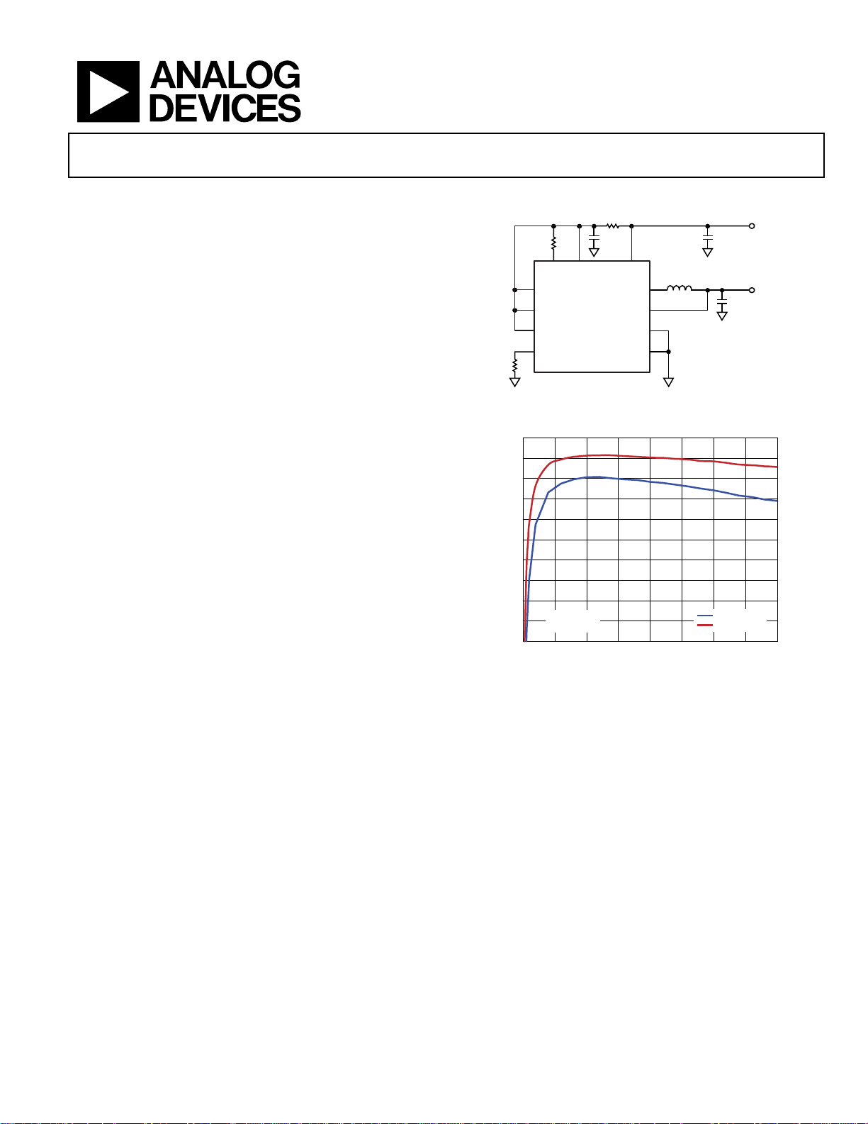
VIN = 5V
f
S
= 600kHz
V
OUT
= 1.2V
V
OUT
= 3.3V
Data Sheet
FEATURES
4 A continuous output current
43 mΩ and 29 mΩ integrated FET
±1.5% output accuracy
Input voltage range: 2.7 V to 6.5 V
Output voltage: 0.6 V to V
Switching frequency
Fixed frequency: 600 kHz or 1.2 MHz
Adjustable frequency: 500 kHz to 1.4 MHz
Synchronizable from 500 kHz to 1.4 MHz
Selectable synchronize phase shift: 0° or 180°
Current mode architecture
Precision enable input
Power-good output
Voltage tracking input
Integrated soft start
Internal compensation
Starts up into a precharged output
UVLO, OVP, OCP, and thermal shutdown
Available in 16-lead, 4 mm × 4 mm LFCSP package
Supported by ADIsimPower™ design tool
IN
6.5 V, 4 A, High Efficiency,
TYPICAL APPLICATIONS CIRCUIT
Figure 1.
APPLICATIONS
Point-of-load conversion
Communications and networking equipment
Industrial and instrumentation
Consumer electronics
GENERAL DESCRIPTION
The ADP2164 is a 4 A, synchronous, step-down dc-to-dc regulator
in a compact 4 mm × 4 mm LFCSP package. The regulator uses a
current mode, constant frequency pulse-width modulation (PWM)
control scheme for excellent stability and transient response.
The input voltage range of the ADP2164 is 2.7 V to 6.5 V. The
output voltage of the ADP2164 is adjustable from 0.6 V to the
input voltage (V
output voltage options: 3.3 V, 2.5 V, 1.8 V, 1.5 V, 1.2 V, and 1.0 V.
responsibility is assumed by Analog Devices for its use, nor for any infringements of patents or other
rights of third parties that may result from its use. Specifications subject to change without noti ce. No
license is granted by implication or otherwise under any patent or patent rights of Analog Devices.
). The ADP2164 is also available in six preset
IN
The ADP2164 integrates a pair of low on-resistance P-channel
and N-channel internal MOSFETs to maximize efficiency and
minimize external component count. The 100% duty cycle
operation allows low dropout voltage at 4 A output current.
The high, 1.2 MHz PWM switching frequency allows the use of
small external components, and the SYNC input enables multiple
ICs to synchronize out of phase to reduce ripple and eliminate
beat frequencies.
Other key features of the ADP2164 include undervoltage lockout
(UVLO), integrated soft start to limit inrush current at startup,
overvoltage protection (OVP), overcurrent protection (OCP),
and thermal shutdown.
One Technology Way, P.O. Box 9106, Norwood, MA 02062-9106, U.S.A.
Tel: 781.329.4700
Figure 2. Efficiency vs. Output Current
www.analog.com
Page 2

ADP2164 Data Sheet
TABLE OF CONTENTS
Features .............................................................................................. 1
Applications ....................................................................................... 1
Typical Applications Circuit ............................................................ 1
General Description ......................................................................... 1
Revision History ............................................................................... 2
Specifications ..................................................................................... 3
Absolute Maximum Ratings ............................................................ 5
Thermal Resistance ...................................................................... 5
ESD Caution .................................................................................. 5
Pin Configuration and Function Descriptions ............................. 6
Typical Performance Characteristics ............................................. 7
Functional Block Diagram ............................................................ 13
Theory of Operation ...................................................................... 14
Control Scheme .......................................................................... 14
Slope Compensation .................................................................. 14
Precision Enable/Shutdown ...................................................... 14
Integrated Soft Start ................................................................... 14
Oscillator and Synchronization ................................................ 14
Power Good ................................................................................ 15
Current Limit and Short-Circuit Protection ............................ 15
Overvoltage Protection (OVP) ................................................. 15
Undervoltage Lockout (UVLO) ............................................... 15
Thermal Shutdown .................................................................... 15
Applications Information .............................................................. 16
ADIsimPower Design Tool ....................................................... 16
Output Voltage Selection ........................................................... 16
Inductor Selection ...................................................................... 16
Output Capacitor Selection....................................................... 16
Input Capacitor Selection .......................................................... 17
Voltage Tracking ......................................................................... 17
Applications Circuits ...................................................................... 18
Outline Dimensions ....................................................................... 19
Ordering Guide .......................................................................... 19
REVISION HISTORY
6/12—Rev. 0 to Rev. A
Changes to Features Section............................................................ 1
Added ADIsimPower Design Tool Section ................................. 16
12/11—Revision 0: Initial Version
Rev. A | Page 2 of 20
Page 3

Data Sheet ADP2164
VIN falling
2.4
2.5 V
FB Bias Current
IFB
0.01
0.1
µA
TRK to FB Offset Voltage
TRK = 0 mV to 500 mV
−15 +15
mV
Minimum Pulse Width
100
ns
SPECIFICATIONS
VIN = PVIN = 3.3 V, EN high, SYNC high, TJ = −40°C to +125°C, unless otherwise noted. Typical values are at TJ = 25°C.
Table 1.
Parameter Symbol Test Conditions/Comments Min Typ Max Unit
VIN AND PVIN PINS
VIN Voltage Range VIN 2.7 6.5 V
PVIN Voltage Range PVIN 2.7 6.5 V
Quiescent Current I
Shutdown Current I
VIN Undervoltage Lockout Threshold UVLO VIN rising 2.6 2.7 V
OUTPUT CHARACTERISTICS Specified by the circuit in Figure 42
Load Regulation IO = 0 A to 4 A 0.05 %/A
Line Regulation IO = 2 A 0.05 %/V
FB PIN
FB Regulation Voltage VFB TJ = −40°C to +125°C 0.591 0.6 0.609 V
SW PIN
High-Side On Resistance1 VIN = PVIN = 3.3 V, ISW = 500 mA 35 52 70 mΩ
VIN = PVIN = 5 V, ISW = 500 mA 30 43 55 mΩ
Low-Side On Resistance1 VIN = PVIN = 3.3 V, ISW = 500 mA 24 32 40 mΩ
VIN = PVIN = 5 V, ISW = 500 mA 20 29 35 mΩ
SW Peak Current Limit High-side switch, PVIN = 3.3 V 5 6.2 7.4 A
SW Maximum Duty Cycle Full frequency 100 %
SW Minimum On Time2 Full frequency 100 ns
TRK PIN
TRK Input Voltage Range 0 600 mV
No switching 895 1100 µA
VIN
VIN = PVIN = 6.5 V, EN = GND 9 12 µA
SHDN
TRK Input Bias Current 100 nA
FREQUENCY
Switching Frequency fS RT = VIN 1.08 1.2 1.32 MHz
RT = GND 540 600 660 kHz
RT = 91 kΩ 480 600 720 kHz
Switching Frequency Range 500 1400 kHz
RT Pin Input High Voltage 1.2 V
RT Pin Input Low Voltage 0.45 V
SYNC PIN
Synchronization Range 0.5 1.4 MHz
Minimum Off Time 100 ns
Input High Voltage 1.2 V
Input Low Voltage 0.4 V
PGOOD PIN
Power-Good Range FB rising threshold 105 110 115 %
FB rising hysteresis 2.5 %
FB falling threshold 85 90 95 %
FB falling hysteresis 2.5 %
Power-Good Deglitch Time From FB to PGOOD 16 Clock
Power-Good Leakage Current V
Power-Good Output Low Voltage I
= 5 V 0.1 1 µA
PGOOD
= 1 mA 170 220 mV
PGOOD
cycles
Rev. A | Page 3 of 20
Page 4

ADP2164 Data Sheet
Parameter Symbol Test Conditions/Comments Min Typ Max Unit
INTEGRATED SOFT START
Soft Start Time All switching frequencies 2048 Clock
cycles
EN PIN
EN Input Rising Threshold 1.12 1.2 1.28 V
EN Input Hysteresis 100 mV
EN Pull-Down Resistor 1 MΩ
THERMAL SHUTDOWN
Thermal Shutdown Threshold TJ increasing 140 °C
Thermal Shutdown Hysteresis 15
1
Pin-to-pin measurements.
2
Guaranteed by design.
°C
Rev. A | Page 4 of 20
Page 5
Data Sheet ADP2164
FB, SYNC, TRK, RT, EN, PGOOD
−0.3 V to +7 V
θ
ABSOLUTE MAXIMUM RATINGS
Table 2.
Parameter Rating
PVIN, VIN, SW −0.3 V to +7 V
PGND to GND −0.3 V to +0.3 V
Operating Junction Temperature Range −40°C to +125°C
Storage Temperature Range −65°C to +150°C
Soldering Conditions JEDEC J-STD-020
Stresses above those listed under Absolute Maximum Ratings
may cause permanent damage to the device. This is a stress
rating only; functional operation of the device at these or any
other conditions above those indicated in the operational
section of this specification is not implied. Exposure to absolute
maximum rating conditions for extended periods may affect
device reliability.
THERMAL RESISTANCE
θJA is measured using natural convection on a JEDEC 4-layer
board. The exposed pad is soldered to the printed circuit board
with thermal vias.
Table 3. Thermal Resistance
Package Type
16-Lead LFCSP 38.3 °C/W
Unit
JA
ESD CAUTION
Rev. A | Page 5 of 20
Page 6
ADP2164 Data Sheet
S
D
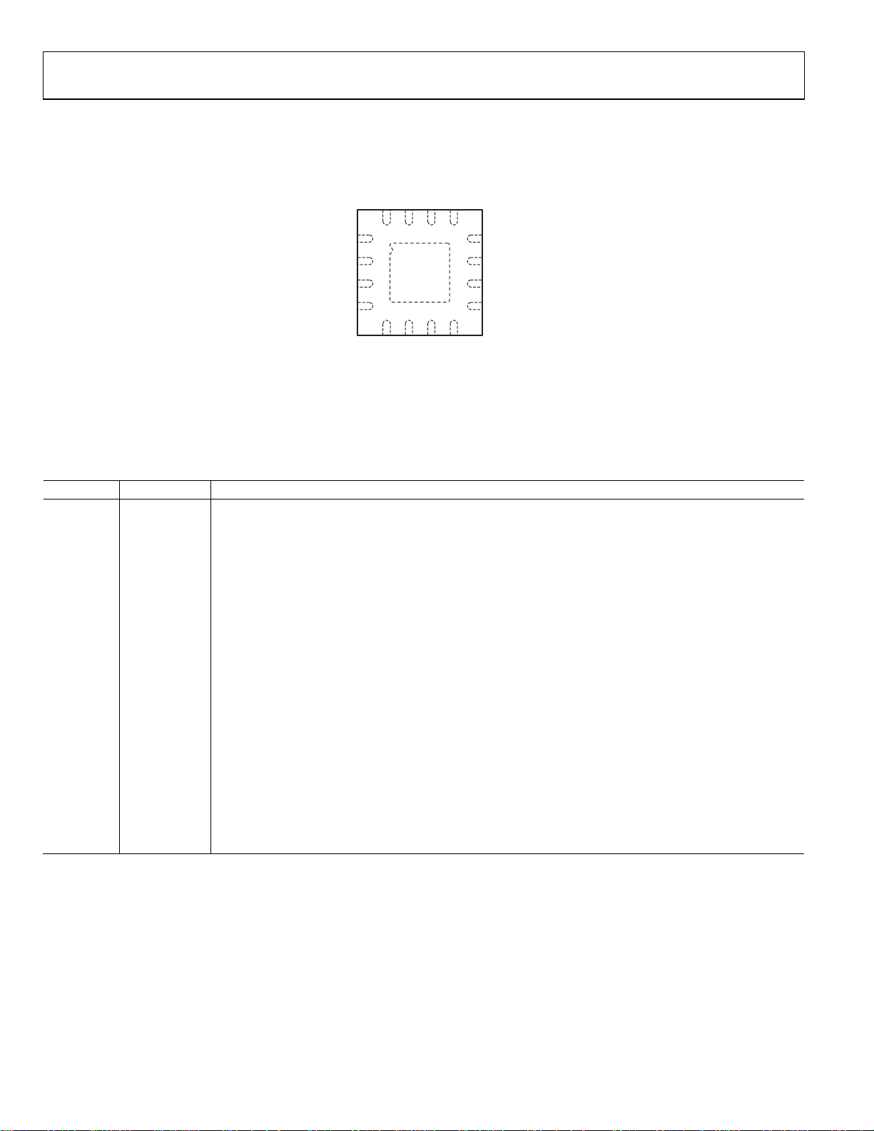
PIN CONFIGURATION AND FUNCTION DESCRIPTIONS
PGOO
EN
VIN
PVIN
16
15
1
YNC
2
RT
3
TRK
4
FB
NOTES
1. THE EXPOSED PAD SHOULD BE SOLDERED
TO AN EXTERNAL GROUND PLANE UNDER
THE IC FOR THERMAL DISSIPATION.
ADP2164
TOP VIEW
(Not to S cale)
6
5
D
GND
PGN
Figure 3. Pin Configuration
Table 4. Pin Function Descriptions
Pin No. Mnemonic Description
1 SYNC
Synchronization Input. To synchronize the switching frequency to an external clock, connect this pin to an
external clock with a frequency of 500 kHz to 1.4 MHz (see the Oscillator and Synchronization section for
more information).
2 RT
Frequency Setting. To select a switching frequency of 600 kHz, connect this pin to GND; to select a switching
frequency of 1.2 MHz, connect this pin to VIN. To program the frequency from 500 kHz to 1.4 MHz, connect a
resistor from this pin to GND (see the Oscillator and Synchronization section for more information).
3 TRK
Tracking Input. To track a master voltage, connect the TRK pin to a voltage divider from the master voltage. If
the tracking function is not used, connect the TRK pin to VIN. For more information, see the Voltage Tracking
section.
4 FB
Feedback Voltage Sense Input. Connect this pin to a resistor divider from V
connect this pin directly to V
OUT
.
5 GND Analog Ground. Connect to the ground plane.
6, 7, 8 PGND Power Ground. Connect to the ground plane and to the output return side of the output capacitor.
9, 10, 11 SW Switch Node Output. Connect to the output inductor.
12, 13 PVIN
Power Input Pin. Connect this pin to the input power source. Connect a bypass capacitor between this pin
and PGND.
14 VIN
Bias Voltage Input Pin. Connect a bypass capacitor between this pin and GND; connect a small (10 Ω) resistor
between this pin and PVIN.
15 EN
Precision Enable Pin. The external resistor divider can be used to set the turn-on threshold. To enable the
part automatically, connect the EN pin to VIN. This pin has a 1 MΩ pull-down resistor to GND.
16 PGOOD Power-Good Output (Open Drain). Connect this pin to a resistor from any pull-up voltage lower than 6.5 V.
17 (EPAD) Exposed Pad The exposed pad should be soldered to an external ground plane under the IC for thermal dissipation.
13
14
PVIN
12
SW
11
10
SW
9
SW
8
7
GND
PGND
P
09944-003
. For the preset output version,
OUT
Rev. A | Page 6 of 20
Page 7

Data Sheet ADP2164
100
90
80
70
60
50
40
30
0 1 2 3 4
OUTPUT CURRE NT (A)
EFFICIENCY (%)
09944-004
INDUCTOR: COILCRAFT
MSS1038-152NLB
V
OUT
= 0.6V
V
OUT
= 1.0V
V
OUT
= 1.2V
V
OUT
= 1.8V
V
OUT
= 2.5V
100
90
80
70
60
50
40
30
0 1 2 3 4
OUTPUT CURRE NT (A)
EFFICIENCY (%)
09944-005
INDUCTOR: COILCRAFT
MSS1038-102NLB
V
OUT
= 0.6V
V
OUT
= 1.0V
V
OUT
= 1.2V
V
OUT
= 1.8V
V
OUT
= 2.5V
1050
1000
950
900
850
800
750
2.7 3.1 3.5 3.9 4.3 4.7 5.1 5.5 5.9 6.3
V
IN
(V)
QUIESCENT CURRENT (µA)
09944-006
TJ = –40°C
T
J
= +25°C
T
J
= +125°C
100
90
80
70
60
50
40
30
0 1 2 3 4
OUTPUT CURRENT (A)
EFFICIENCY (%)
09944-007
INDUCTOR: COILCRAFT
MSS1038-152NLB
V
OUT
= 0.6V
V
OUT
= 1.0V
V
OUT
= 1.2V
V
OUT
= 1.8V
V
OUT
= 2.5V
V
OUT
= 3.3V
100
90
80
70
60
50
40
30
0 1 2 3 4
OUTPUT CURRE NT (A)
EFFICIENCY (%)
09944-008
INDUCTOR: COILCRAFT
MSS1038-102NLB
V
OUT
= 1.0V
V
OUT
= 1.2V
V
OUT
= 1.8V
V
OUT
= 2.5V
V
OUT
= 3.3V
11
10
9
8
7
6
5
4
2.7 3.1 3.5 3.9 4.3 4.7 5.1 5.5 5.9 6.3
V
IN
(V)
SHUTDOWN CURRE NT (µA)
09944-009
TJ = –40°C
T
J
= +25°C
T
J
= +125°C
TYPICAL PERFORMANCE CHARACTERISTICS
TJ = 25°C, VIN = 5 V, V
= 1.2 V, L = 1 µH, CIN = 47 µF, C
OUT
= 100 µF, unless otherwise noted.
OUT
Figure 4. Efficiency vs. Output Current, VIN = 3.3 V, fS = 600 kHz
Figure 5. Efficiency vs. Output Current, VIN = 3.3 V, fS = 1.2 MHz
Figure 7. Efficiency vs. Output Current, VIN = 5 V, fS = 600 kHz
Figure 8. Efficiency vs. Output Current, VIN = 5 V, fS = 1.2 MHz
Figure 6. Quiescent Current vs. VIN (No Switching)
Figure 9. Shutdown Current vs. VIN
Rev. A | Page 7 of 20
Page 8

ADP2164 Data Sheet
606
605
604
603
602
601
600
599
598
597
596
595
594
–40 –20 0 20 40 60 80 100 120
TEMPERATURE (°C)
FEEDBACK VOLTAGE (mV)
09944-010
80
70
60
50
40
30
20
2.7 3.1 3.5 3.9 4.3 4.7 5.1 5.5 5.9 6.3
V
IN
(V)
PFET RESISTOR (mΩ)
09944-011
TJ = –40°C
T
J
= +25°C
T
J
= +125°C
1300
1275
1250
1225
1200
1175
1100
1150
1125
FREQUENCY ( kHz )
2.7 3.1 3.5 3.9 4.3 4.7 5.1 5.5 5.9 6.3
V
IN
(V)
09944-012
TJ = –40°C
T
J
= +25°C
T
J
= +125°C
1.30
1.28
1.26
1.24
1.22
1.20
1.18
1.16
1.14
1.12
1.10
1.08
1.06
1.04
1.02
1.00
–40 –20 0 20 40 60 80 100 120
TEMPERATURE (°C)
ENABLE THRES HOLD (V)
09944-013
RISING
FALLING
60
50
40
30
20
10
2.7 3.1 3.5 3.9 4.3 4.7 5.1 5.5 5.9 6.3
V
IN
(V)
NFET RESISTOR (mΩ)
09944-014
T
J
= –40°C
T
J
= +25°C
T
J
= +125°C
650
640
630
620
610
600
590
580
550
570
560
FREQUENCY ( kHz )
2.7 3.1 3.5 3.9 4.3 4.7 5.1 5.5 5.9 6.3
V
IN
(V)
09944-015
TJ = –40°C
T
J
= +25°C
T
J
= +125°C
Figure 10. Feedback Voltage vs. Temperature, VIN = 3.3 V
Figure 11. PFET Resistor vs. VIN (Pin-to-Pin Measurements)
Figure 13. EN Threshold vs. Temperature
Figure 14. NFET Resistor vs. VIN (Pin-to-Pin Measurements)
Figure 12. Switching Frequency vs. VIN, fS = 1.2 MHz (RT = VIN)
Figure 15. Switching Frequency vs. VIN, fS = 600 kHz (RT = GND)
Rev. A | Page 8 of 20
Page 9

Data Sheet ADP2164
650
640
630
620
610
600
590
580
570
560
550
FREQUENCY ( kHz )
09944-016
2.7 3.1 3.5 3.9 4.3 4.7 5.1 5.5 5.9 6.3
V
IN
(V)
TJ = –40°C
T
J
= +25°C
T
J
= +125°C
6.8
6.6
6.4
6.2
6.0
5.8
5.6
5.4
5.2
–40 –20 0 20 40 60 80 100 120
TEMPERATURE (°C)
PEAK CURRENT LIMIT (A)
09944-017
09944-018
CH1 500mV CH2 5.00V
CH3 5.00V CH4 2.00A Ω
M 1.00ms A CH3 2.50V
1
3
4
2
T 20.20%
T
EN
PGOOD
I
L
V
OUT
2.70
2.68
2.66
2.64
2.62
2.60
2.58
2.56
2.54
2.52
2.50
2.48
2.46
2.44
2.42
2.40
–40 –20 0 20 40 60 80 100 120
TEMPERATURE (°C)
UVLO THRE S HOLD (V)
09944-019
RISING
FALLING
7.0
6.8
6.6
6.4
6.2
6.0
5.8
5.6
5.4
2.7 3.1 3.5 3.9 4.3 4.7 5.1 5.5 5.9 6.3
V
IN
(V)
09944-020
PEAK CURRENT LIMIT (A)
09944-021
CH1 500mV CH2 5.00V
CH3 5.00V CH4 2.00A Ω
M 1.00ms A CH3 2.50V
1
3
4
2
T 20.20%
T
EN
PGOOD
I
L
V
OUT
Figure 16. Switching Frequency vs. VIN, fS = 600 kHz (RT = 91 kΩ)
Figure 17. Peak Current Limit vs. Temperature, VIN = 3.3 V
Figure 19. UVLO Threshold vs. Temperature, VIN = 3.3 V
Figure 20. Peak Current Limit vs. VIN, TJ = 25°C
Figure 18. Soft Start with Full Load, VIN = 5 V, V
= 1.2 V, fS = 1.2 MHz
OUT
Figure 21. Soft Start with Precharged Output Voltage, VIN = 5 V, fS = 1.2 MHz
Rev. A | Page 9 of 20
Page 10

ADP2164 Data Sheet
I
O
09944-022
CH1 100mV
CH4 2.00A Ω
M 200µs ACH4 2. 52A
4
1
T 20.20%
T
B
W
V
OUT
(AC)
09944-023
CH1 5.00V CH2 2.00V M 400ns A CH1 2.50V
1
2
T 60.40%
T
SW
SYNC
09944-024
CH1 500mV CH2 5.00V
CH4 5.00A Ω
M 2.00ms A CH1 680mV
2
4
1
T 30.20%
T
SW
V
OUT
I
L
B
W
B
W
I
O
09944-025
CH1 100mV
CH4 2.00A Ω
M 200µs A CH4 2.52A
4
1
T 20.20%
B
W
T
V
OUT
(AC)
09944-026
CH1 5.00V CH2 2.00V M 400ns A CH1 2.50V
1
2
T 60.40%
SW
T
SYNC
09944-027
CH1 500mV CH2 5.00V
CH4 5.00 AΩ
M 2.00ms A CH1 680mV
2
4
1
T 60.60%
T
SW
V
OUT
I
L
B
W
B
W
Figure 22. Load Transient, 0.5 A to 3.5 A Load Step,
V
= 5 V, V
IN
= 1.2 V, fS = 1.2 MHz
OUT
Figure 23. ADP2164 Synchronized to 1 MHz, in Phase
Figure 25. Load Transient, 0.5 A to 3.5 A Load Step,
V
= 5 V, V
IN
= 1.2 V, fS = 600 kHz
OUT
Figure 26. ADP2164 Synchronized to 1 MHz, 180° out of Phase
Figure 24. Output Short
Figure 27. Output Short Recovery
Rev. A | Page 10 of 20
Page 11

Data Sheet ADP2164
09944-028
CH2 500mV
CH4 500mV
M 2.00ms A CH2 820mV
4
T 40.40%
T
TRK
FB
B
W
B
W
60
48
36
24
12
0
–12
–24
–36
–48
–60
200
160
120
80
40
0
–40
–80
–120
–160
–200
1k 10k
1 2
100k 1M
FREQUENCY ( Hz )
MAGNITUDE ( dB)
PHASE (Degrees)
09944-029
CROSS FREQUENCY: 57kHz
PHASE MARGI N: 67°
PHASE
MAGNITUDE
60
48
36
24
12
0
–12
–24
–36
–48
–60
200
160
120
80
40
0
–40
–80
–120
–160
–200
1k 10k
1 2
100k 1M
FREQUENCY ( Hz )
MAGNITUDE ( dB)
PHASE (Degrees)
09944-030
CROSS FREQUENCY: 52kHz
PHASE MARGI N: 69°
PHASE
MAGNITUDE
09944-031
CH1 5.00mV CH2 5.00V
CH4 2.00A Ω
M 400ns A CH2 3.30V
2
1
4
T 30.60%
T
SW
V
OUT
I
L
60
48
36
24
12
0
–12
–24
–36
–48
–60
200
160
120
80
40
0
–40
–80
–120
–160
–200
1k 10k
1 2
100k 1M
FREQUENCY ( Hz )
MAGNITUDE ( dB)
PHASE (Degrees)
09944-032
CROSS FREQUENCY: 61kHz
PHASE MARGI N: 69°
PHASE
MAGNITUDE
60
48
36
24
12
0
–12
–24
–36
–48
–60
200
160
120
80
40
0
–40
–80
–120
–160
–200
1k 10k
1 2
100k 1M
FREQUENCY ( Hz )
MAGNITUDE ( dB)
PHASE (Degrees)
09944-033
CROSS FREQUENCY: 61kHz
PHASE MARGI N: 66°
PHASE
MAGNITUDE
Figure 28. Tracking Function
Figure 29. Bode Plot at VIN = 5 V, V
L = 0.68 μH, C
= 1.0 V, IO = 4 A, fS = 1.2 MHz,
OUT
= 2 × 100 μF
OUT
Figure 31. Steady Waveform, VIN = 5 V, V
Figure 32. Bode Plot at VIN = 5 V, V
L = 0.68 μH, C
OUT
= 47 μF + 100 μF
OUT
= 1.2 V, fS = 1.2 MHz
OUT
= 1.2 V, IO = 4 A, fS = 1.2 MHz,
Figure 30. Bode Plot at VIN = 5 V, V
L = 1 μH, C
= 1.5 V, IO = 4 A, fS = 1.2 MHz,
OUT
= 47 μF + 100 μF
OUT
Figure 33. Bode Plot at VIN = 5 V, V
L = 1 μH, C
= 1.8 V, IO = 4 A, fS = 1.2 MHz,
OUT
= 100 μF
OUT
Rev. A | Page 11 of 20
Page 12

ADP2164 Data Sheet
60
48
36
24
12
0
–12
–24
–36
–48
–60
200
160
120
80
40
0
–40
–80
–120
–160
–200
1k 10k
1 2
100k 1M
FREQUENCY ( Hz )
MAGNITUDE ( dB)
PHASE (Degrees)
09944-034
CROSS FREQUENCY: 83kHz
PHASE MARGI N: 60°
PHASE
MAGNITUDE
60
48
36
24
12
0
–12
–24
–36
–48
–60
200
160
120
80
40
0
–40
–80
–120
–160
–200
1k 10k
1 2
100k 1M
FREQUENCY ( Hz )
MAGNITUDE ( dB)
PHASE (Degrees)
09944-035
CROSS FREQUENCY: 68kHz
PHASE MARGI N: 65°
PHASE
MAGNITUDE
Figure 34. Bode Plot at VIN = 5 V, V
L = 1 μH, C
= 2.5 V, IO = 4 A, fS = 1.2 MHz,
OUT
= 47 μF
OUT
Figure 35. Bode Plot at VIN = 5 V, V
L = 1 μH, C
= 3.3 V, IO = 4 A, fS = 1.2 MHz,
OUT
= 47 μF
OUT
Rev. A | Page 12 of 20
Page 13

Data Sheet ADP2164
09944-036
SOFT
START
+
+
+
–
G
M
Z
COMP
ERROR AMP
LOGIC
CONTROL
0.6V
PFET
NFET
0.66V
0.54V
+
–
+
–
PMOS
CURRENT
SENSE AMP
NMOS
CURRENT
SENSE AMP
OSCILLATOR
SLOPE
COMPENSATION
REGULATOR
UVLO
ADP2164
PGND
CLK
RTSYNC
VIN EN PVIN
SW
GND
PGOOD
FB
TRK
FUNCTIONAL BLOCK DIAGRAM
Figure 36. Functional Block Diagram
Rev. A | Page 13 of 20
Page 14

ADP2164 Data Sheet
(kHz)
000,54
)(k
S
f
RT =Ω
1600
1400
1200
1000
800
600
400
200
20 40 60 80 100 120 140 160 180
RT RESISTOR (kΩ)
FREQUENCY ( kHz )
09944-037
THEORY OF OPERATION
The ADP2164 is a step-down dc-to-dc regulator that uses
a fixed-frequency, peak current mode architecture with an
integrated high-side switch and low-side synchronous rectifier.
The high switching frequency and tiny, 16-lead, 4 mm × 4 mm
LFCSP package provide a small, step-down dc-to-dc regulator
solution. The integrated high-side switch (P-channel MOSFET)
and synchronous rectifier (N-channel MOSFET) yield high
efficiency.
The ADP2164 operates with an input voltage from 2.7 V to 6.5 V
and regulates the output voltage down to 0.6 V. T he ADP2164 is
also available with preset output voltage options of 3.3 V, 2.5 V,
1.8 V, 1.5 V, 1.2 V, and 1.0 V.
CONTROL SCHEME
The ADP2164 uses a fixed-frequency, peak current mode
PWM control architecture. At the start of each oscillator cycle,
the P-channel MOSFET switch is turned on, placing a positive
voltage across the inductor. Current in the inductor increases
until the current sense signal crosses the peak inductor current
level, turns off the P-channel MOSFET switch, and turns on the
N-channel MOSFET synchronous rectifier. This action places a
negative voltage across the inductor, causing the inductor current
to decrease. The synchronous rectifier stays on for the rest of
the cycle.
The peak inductor current level is set by the compensation
(COMP) voltage. The COMP voltage is the output of a transconductance error amplifier that compares the feedback voltage
with an internal 0.6 V reference (see Figure 36).
INTEGRATED SOFT START
The ADP2164 has integrated soft start circuitry to limit the
output voltage rise time and reduce inrush current at startup.
The soft start time is set at 2048 clock cycles.
If the output voltage is precharged before the part is turned
on, the ADP2164 prevents a reverse inductor current—which
would discharge the output capacitor—until the soft start
voltage exceeds the voltage on the FB pin.
OSCILLATOR AND SYNCHRONIZATION
The ADP2164 switching frequency is controlled by the RT pin.
If the RT pin is connected to GND, the switching frequency is
set to 600 kHz. If the RT pin is connected to VIN, the switching
frequency is set to 1.2 MHz.
Connecting a resistor from RT to GND allows programming
of the switching frequency from 500 kHz to 1.4 MHz. Use the
following equation to set the switching frequency:
Figure 37 shows the typical relationship between the switching
frequency and the RT resistor.
SLOPE COMPENSATION
To prevent subharmonic oscillations, slope compensation
stabilizes the internal current control loop of the ADP2164
when the part operates at or beyond a 50% duty cycle. Slope
compensation is implemented by summing an artificial voltage
ramp with the current sense signal during the on time of the
P-channel MOSFET switch. This voltage ramp depends on the
output voltage. When operating at high output voltages, slope
compensation increases. The slope compensation ramp value
determines the minimum inductor value that can be used to
prevent subharmonic oscillations.
PRECISION ENABLE/SHUTDOWN
The EN pin is a precision analog input that enables the device
when the voltage exceeds 1.2 V (typical); this pin has 100 mV
hysteresis. When the enable voltage falls below 1.1 V (typical),
the part turns off. To force the ADP2164 to start automatically
when input power is applied, connect the EN pin to the VIN pin.
When the ADP2164 is shut down, the soft start capacitor is
discharged. This causes a new soft start cycle to begin when
the part is reenabled.
An internal pull-down resistor (1 MΩ) prevents accidental
enabling of the part if the EN input is left floating.
Figure 37. Switching Frequency vs. RT Resistor
To synchronize the ADP2164, drive an external clock at the
SYNC pin. The frequency of the external clock can be in the
range of 500 kHz to 1.4 MHz.
When the SYNC pin is driven by an external clock, the user
can configure the switching frequency to be in phase with the
external clock or 180° out of phase with the external clock, as
follows:
• If the RT pin is connected to GND or to a resistor, the
switching frequency is in phase with the external clock.
• If the RT pin is connected to VIN, the switching frequency
is 180° out of phase with the external clock.
Rev. A | Page 14 of 20
Page 15

Data Sheet ADP2164
POWER GOOD
PGOOD is an active high, open-drain output and requires a
resistor to pull it up to the logic supply voltage. PGOOD high
indicates that the voltage on the FB pin (and, therefore, the
output voltage) is within 10% of the desired value. PGOOD low
indicates the opposite. There is a 16-cycle waiting period after
the FB voltage is detected as being out of bounds. If FB returns
to within the ±10% range, it is ignored by the PGOOD circuitry.
CURRENT LIMIT AND SHORT-CIRCUIT PROTECTION
The ADP2164 has a peak current limit protection circuit to
prevent current runaway. The peak current limit is 6.2 A. When
the inductor current reaches the peak current limit, the high-side
MOSFET turns off and the low-side MOSFET turns on until the
next cycle begins.
The overcurrent counter is incremented by 1 at each peak
current limit event. If the overcurrent counter exceeds 10, the
part enters hiccup mode, and the high-side FET and low-side
FET are both turned off. The part remains in this mode for
4096 clock cycles and then attempts to restart using soft start.
If the current limit fault has cleared, the part resumes normal
operation. If the current limit fault has not cleared, the part
reenters hiccup mode after first counting 10 current limit
violations.
OVERVOLTAGE PROTECTION (OVP)
Overvoltage protection (OVP) circuitry is integrated in the
ADP2164. The output voltage is continuously monitored by
a comparator through the FB pin, which is at 0.6 V (typical)
under normal operation. The comparator is activated when the
FB voltage exceeds 0.66 V (typical), thus indicating an output
overvoltage condition. If the voltage remains above the OVP
threshold for 16 clock cycles, the high-side MOSFET turns off
and the low-side MOSFET turns on until the current through it
reaches the −1.3 A current limit. Both MOSFETs remain in the
off state until FB falls below 0.54 V (typical), after which the
part restarts. The behavior of PGOOD under this condition is
described in the Power Good section.
UNDERVOLTAGE LOCKOUT (UVLO)
Undervoltage lockout (UVLO) circuitry is integrated in the
ADP2164. If the input voltage falls below 2.5 V, th e ADP2164
shuts down, and both the power switch and the synchronous
rectifier turn off. When the voltage rises above 2.6 V again,
the soft start is initiated, and the part is enabled.
THERMAL SHUTDOWN
If the ADP2164 junction temperature rises above 140°C, the
thermal shutdown circuit turns off the regulator. Extreme junction temperatures can be the result of high current operation,
poor circuit board design, and/or high ambient temperature.
When thermal shutdown occurs, a 15°C hysteresis ensures that
the ADP2164 does not return to operation until the on-chip
temperature falls below 125°C. Soft start is initiated when the
part comes out of thermal shutdown.
Rev. A | Page 15 of 20
Page 16

ADP2164 Data Sheet
09944-042
ADP2164ACPZ
C
IN
47µF
X5R
10V
C
OUT1
47µF
X5R
6.3V
C
OUT2
100µF
X5R
6.3V
V
OUT
1.2V
4A
V
IN
3.3V
SYNC
TRK
FB
RT
SW
SW
SW
PVIN
GND PGND PGND PGND
L
0.8µH
R
TOP
10kΩ
R
BOT
10kΩ
L: MSS1048-801NL COIL CRAFT
C
IN
: C3225X5R1A476M TDK
C
OUT1
: C3225X5R0J476M TDK
C
OUT2
: C3225X5R0J107M TDK
12
11
10
94
3
2
1
5 6 7 8
PGOOD
C1
0.1µF
EN
R1
10Ω
R2
10kΩ
PVIN
16 15
VIN
14
13
+×=
BOT
TOP
OUT
R
R
V 16.0
( )
S
L
OUT
IN
fI
DVV
L
×∆
×−
=
2
L
OPEAK
III∆
+=
××
+×∆=∆
S
OUT
L
OUT
fC
ESRIV
8
1
5
1.8 1 100
APPLICATIONS INFORMATION
ADISIMPOWER DESIGN TOOL
The ADP2164 is supported by ADIsimPower design tool set.
ADIsimPower is a collection of tools that produce complete
power designs optimized for a specific design goal. The tools
enable the user to generate a full schematic, bill of materials,
and calculate performance in minutes. ADIsimPower can
optimize designs for cost, area, efficiency, and parts count
while taking into consideration the operating conditions and
limitations of the IC and all real external components. For
more information about ADIsimPower design tools, refer to
www.analog.com/ADIsimPower. The tool set is available from
this website, and users can also request an unpopulated board
through the tool.
The typical application circuit for the ADP2164 is shown in
Figure 38.
where:
V
is the input voltage.
IN
V
is the output voltage.
OUT
ΔI
is the inductor current ripple.
L
f
is the switching frequency.
S
D is the duty cycle (V
The ADP2164 uses slope compensation in the current control
loop to prevent subharmonic oscillations when the duty cycle
is larger than 50%. The internal slope compensation limits the
minimum inductor value.
The negative current limit (−1.3 A) also limits the minimum
inductor value. The inductor current ripple (ΔI
the selected inductor should not exceed 2.6 A.
The peak inductor current should be kept below the peak current
limit threshold and is calculated using the following equation:
OUT/VIN
).
) calculated by
L
Figure 38. Typical Application Circuit
OUTPUT VOLTAGE SELECTION
The output voltage of the adjustable version of the ADP2164 is
set by an external resistive voltage divider using the following
equation:
To limit output voltage accuracy degradation due to FB bias
current (0.1 µA maximum) to less than 0.5% (maximum),
ensure that R
INDUCTOR SELECTION
The inductor value is determined by the operating frequency,
input voltage, output voltage, and ripple current. A small inductor
value provides larger inductor current ripple and fast transient
response but degrades efficiency; a large inductor value provides
small inductor current ripple and good efficiency but slows
transient response. For a reasonable trade-off between transient
response and efficiency, the inductor current ripple, ΔI
set to one-third the maximum load current. The inductor value
is calculated using the following equation:
is less than 30 kΩ.
BOT
, is typically
L
Ensure that the rms current of the selected inductor is greater
than the maximum load current and that its saturation current
is greater than the peak current limit of the converter.
OUTPUT CAPACITOR SELECTION
The output capacitor value is determined by the output voltage
ripple, load step transient, and loop stability. The output ripple
is determined by the ESR and the capacitance.
The load step transient response depends on the inductor, the
output capacitor, and the current control loop.
The ADP2164 has integrated loop compensation for simple
power design. Tab l e 5 and Table 6 show the recommended
values for inductors and capacitors for the ADP2164 based
on the input and output voltages for the part. X5R or X7R
dielectric ceramic capacitors are highly recommended.
Table 5. Recommended L and C
VIN (V) V
3.3 1.0 0.8 100 + 100
3.3 1.2 0.8 100 + 47
3.3 1.5 1 100 + 47
3.3 1.8 1 100
3.3 2.5 1 47
5 1.0 0.8 100 + 100
5 1.2 0.8 100 + 47
5 1.5 1 100 + 47
5 2.5 1 47
5 3.3 1 47
Rev. A | Page 16 of 20
Values at fS = 1.2 MHz
OUT
(V) L (µH) C
OUT
(µF)
OUT
Page 17

Data Sheet ADP2164
5
2.5
1.5
100
( )
DDII
ORMS
−××= 1
09944-039
ADP2164
R
TOP
R
BOT
R
TRKT
R
TRKB
V
SLAVE
V
MASTER
TRK
FB
09944-040
VOLTAGE
TIME
V
SLAVE
V
MASTER
09944-041
VOLTAGE
TIME
V
SLAVE
V
MASTER
TRKB
TRKT
BOT
TOP
MASTER
SLAVE
R
R
R
R
V
V
+
+
=
1
1
Table 6. Recommended L and C
VIN (V) V
(V) L (µH) C
OUT
Values at fS = 600 kHz
OUT
(µF)
OUT
3.3 1.0 1 100 + 100
3.3 1.2 1 100 + 100
3.3 1.5 1 100 + 47
3.3 1.8 1 100 + 47
3.3 2.5 1 100
5 1.0 1 100 + 100
5 1.2 1.5 100 + 100
5 1.5 1.5 100 + 47
5 1.8 1.5 100 + 47
5 3.3 1.5 100
Higher or lower values of inductors and output capacitors can
be used in the regulator, but system stability and load transient
performance must be verified.
Table 7 and Ta b l e 8 list some recommended inductors and
capacitors for the ADP2164.
Table 7. Recommended Inductors
Manufacturer Part No.
Coilcraft® MSS1038, MSS1048, MSS1260
Sumida CDRH103R, CDRH104R, CDRH105R
VOLTAGE TRACKING
The ADP2164 includes a tracking feature that allows the
ADP2164 output (slave voltage) to be configured to track
an external voltage (master voltage), as shown in Figure 39.
BOT
.
Figure 39. Voltage Tracking
Coincident Tracking
A common requirement is coincident tracking, as shown in
Figure 40. Coincident tracking limits the slave output voltage
to the same value as the master voltage until the slave output
voltage reaches regulation. Connect the TRK pin to a resistor
divider driven from the master voltage, as shown in Figure 39.
For coincident tracking, set R
TRKT
= R
TOP
and R
TRKB
= R
Table 8. Recommended Capacitors
Manufacturer Part N o. Description
Murata GRM32ER60J107ME20 100 µF, 6. 3 V, X5R, 1210
Murata GRM32ER60J476ME20 47 µF, 6.3 V, X5R, 1210
TDK C3225X5R0J107M 100 µF, 6 .3 V, X5R, 1210
TDK C3225X5R0J476M 47 µF, 6.3 V, X5R, 1210
INPUT CAPACITOR SELECTION
The input capacitor reduces the input voltage ripple caused by
the switch current on PVIN. Place the input capacitor as close
as possible to the PVIN pins. A 22 µF or 47 µF ceramic capacitor
is recommended. The rms current rating of the input capacitor
should be larger than the value calculated using the following
equation:
where D is the duty cycle.
Figure 40. Coincident Tracking
Ratiometric Tracking
Ratiometric tracking is shown in Figure 41. The slave output is
limited to a fraction of the master voltage. In this application, the
slave and master voltages reach their final values at the same time.
Figure 41. Ratiometric Tracking
The ratio of the slave output voltage to the master voltage is a
function of the two dividers.
Rev. A | Page 17 of 20
Page 18

ADP2164 Data Sheet
09944-042
ADP2164ACPZ
C
IN
47µF
X5R
10V
C
OUT1
47µF
X5R
6.3V
C
OUT2
100µF
X5R
6.3V
V
OUT
1.2V
4A
V
IN
3.3V
SYNC
TRK
FB
RT
SW
SW
SW
PVIN
GND PGND PGND PGND
L
0.8µH
R
TOP
10kΩ
R
BOT
10kΩ
L: MSS1048-801NL COILCRAFT
C
IN
: C3225X5R1A476M TDK
C
OUT1
: C3225X5R0J476M TDK
C
OUT2
: C3225X5R0J107M TDK
12
11
10
94
3
2
1
5 6 7 8
PGOOD
C1
0.1µF
EN
R1
10Ω
R2
10kΩ
PVIN
16 15
VIN
14
13
09944-044
ADP2164ACPZ
C
IN
47µF
X5R
10V
C
OUT
100µF
X5R
6.3V
V
OUT
1.8V
4A
V
IN
5V
SYNC
TRK
FB
RT
SW
SW
SW
PVIN
GND PGND PGND PGND
L
1µH
1MHz
EXT
CLOCK
R
TOP
20kΩ
R
BOT
10kΩ
12
11
10
94
3
2
1
5 6 7 8
PGOOD
C1
0.1µF
EN
R1
10Ω
R2
10kΩ
PVIN
16 15
VIN
14
13
L: MSS1038-102NL COILCRAFT
C
IN
: C3225X5R1A476M TDK
C
OUT
: C3225X5R0J107M TDK
09944-046
ADP2164ACPZ-1.2
C
IN
47µF
X5R
10V
V
OUT
1.2V
4A
V
IN
5V
SYNC
TRK
FB
RT
SW
SW
SW
PVIN
GND PGND PGND PGND
L
0.8µH
L: MSS1048-801NL COILCRAFT
C
IN
: C3225X5R1A476M TDK
C
OUT1
: C3225X5R0J476M TDK
C
OUT2
: C3225X5R0J107M TDK
12
11
10
94
3
2
1
5 6 7 8
PGOOD
C1
0.1µF
EN
R1
10Ω
R2
10kΩ
PVIN
16 15
VIN
14
13
C
OUT1
47µF
X5R
6.3V
C
OUT2
100µF
X5R
6.3V
09944-043
ADP2164ACPZ
C
IN
47µF
X5R
10V
C
OUT
47µF
X5R
6.3V
V
OUT
3.3V
4A
V
IN
5V
SYNC
TRK
FB
RT
SW
SW
SW
PVIN
GND PGND PGND PGND
L
1µH
R
T
54kΩ
R
TOP
10kΩ
R
BOT
2.21kΩ
L: MSS1038-102NL COILCRAFT
C
IN
: C3225X5R1A476M TDK
C
OUT
: C3225X5R0J476M TDK
12
11
10
94
3
2
1
5 6 7 8
PGOOD
C1
0.1µF
EN
R1
10Ω
R2
10kΩ
PVIN
16 15
VIN
14 13
09944-045
ADP2164ACPZ
C
IN
47µF
X5R
10V
V
OUT
1.5V
4A
V
IN
5V
SYNC
TRK
FB
RT
SW
SW
SW
PVIN
GND PGND PGND PGND
L
1µH
1MHz
EXT
CLOCK
R
TOP
15kΩ
R
BOT
10kΩ
L: MSS1038-102NL COILCRAFT
C
IN
: C3225X5R1A476M TDK
C
OUT1
: C3225X5R0J476M TDK
C
OUT2
: C3225X5R0J107M TDK
12
11
10
94
3
2
1
5 6 7 8
PGOOD
C1
0.1µF
EN
R1
10Ω
R2
10kΩ
PVIN
16 15
VIN
14
13
C
OUT1
47µF
X5R
6.3V
C
OUT2
100µF
X5R
6.3V
09944-047
ADP2164ACPZ
C
IN
47µF
X5R
10V
C
OUT
47µF
X5R
6.3V
V
OUT
3.3V
4A
V
IN
5V
SYNC
TRK
FB
RT
SW
SW
SW
PVIN
GND PGND PGND PGND
L
1µH
R
TOP
10kΩ
R
BOT
2.21kΩ
R
TRKB
2.21kΩ
R
TRKT
10kΩ
V
MASTER
L: MSS1038-102NL COILCRAFT
C
IN
: C3225X5R1A476M TDK
C
OUT
: C3225X5R0J476M TDK
12
11
10
94
3
2
1
5 6 7 8
PGOOD
C1
0.1µF
EN
R1
10Ω
R2
10kΩ
PVIN
16 15
VIN
14 13
APPLICATIONS CIRCUITS
Figure 42. 1.2 V, 4 A, 1.2 MHz Step-Down Regulator
Figure 43. 1.8 V, 4 A Step-Down Regulator,
Synchronized to 1 MHz, in Phase with the External Clock
Figure 45. 3.3 V, 4 A, 1 MHz Step-Down Regulator
Figure 46. 1.5 V, 4 A Step-Down Regulator, Synchronized to 1 MHz,
180° out of Phase with the External Clock
Figure 44. Fixed 1.2 V, 4 A, 1.2 MHz Step-Down Regulator
Rev. A | Page 18 of 20
Figure 47. 3.3 V, 4 A, 1.2 MHz Step-Down Regulator, Tracking Mode
Page 19

Data Sheet ADP2164
OUTLINE DIMENSIONS
PIN 1
INDICATOR
0.80
0.75
0.70
SEATING
PLANE
4.10
4.00 SQ
3.90
0.65
BSC
0.50
0.40
0.30
0.05 MAX
0.02 NOM
0.20 REF
0.35
0.30
0.25
13
12
9
8
BOTTOM VIEWTOP VIEW
COPLANARITY
0.08
N
1
P
I
D
C
I
A
N
I
16
1
EXPOSED
PAD
FOR PROPER CONNECTION OF
THE EXPOSED PAD, REFER TO
THE PIN CONFIGURATION AND
FUNCTION DESCRIPTIONS
SECTION OF THIS DATA SHEET.
2.60
2.50 SQ
2.40
4
5
R
O
T
COMPLIANTTOJEDEC STANDARDS MO-220-WGGC.
042709-A
Figure 48. 16-Lead Lead Frame Chip Scale Package [LFCSP_WQ]
4 mm × 4 mm Body, Very Very Thin Quad
(CP-16-26)
Dimensions shown in millimeters
ORDERING GUIDE
1
Model
Temperature Range Output Voltage Package Description Package Option
ADP2164ACPZ-R7 −40°C to +125°C Adjustable 16-Lead LFCSP_WQ CP-16-26
ADP2164ACPZ-1.0-R7 −40°C to +125°C 1.0 V 16-Lead LFCSP_WQ CP-16-26
ADP2164ACPZ-1.2-R7 −40°C to +125°C 1.2 V 16-Lead LFCSP_WQ CP-16-26
ADP2164ACPZ-1.5-R7 −40°C to +125°C 1.5 V 16-Lead LFCSP_WQ CP-16-26
ADP2164ACPZ-1.8-R7 −40°C to +125°C 1.8 V 16-Lead LFCSP_WQ CP-16-26
ADP2164ACPZ-2.5-R7 −40°C to +125°C 2.5 V 16-Lead LFCSP_WQ CP-16-26
ADP2164ACPZ-3.3-R7 −40°C to +125°C 3.3 V 16-Lead LFCSP_WQ CP-16-26
ADP2164-EVALZ Evaluation Board
1
Z = RoHS Compliant Part.
Rev. A | Page 19 of 20
Page 20

ADP2164 Data Sheet
©2011–2021 Analog Devices, Inc. All rights reserved. Trademarks and
NOTES
registered trademarks are the property of their respective owners.
D09944-0-6/12(A)
Rev. A | Page 20 of 20
 Loading...