

Page 1
2 A/1.25 A, 1.2 MHz, Synchronous,
V
FEATURES
Continuous output current
ADP2119: 2 A
ADP2120: 1.25 A
145 mΩ and 70 mΩ integrated MOSFETs
Input voltage range from 2.3 V to 5.5 V
Output voltage from 0.6 V to V
±1.5% output accuracy
1.2 MHz fixed switching frequency
Synchronizable between 1 MHz and 2 MHz
Selectable PWM or PFM mode operation
Current mode architecture
Precision threshold enable input
Power-good flag
Voltage tracking
Integrated soft start
Internal compensation
Startup with precharged output
UVLO, OVP, OCP, and thermal shutdown
10-lead, 3 mm × 3 mm LFCSP_WD package
APPLICATIONS
Point of load conversion
Communications and networking equipment
Industrial and instrumentation
Consumer electronics
Medical applications
GENERAL DESCRIPTION
The ADP2119/ADP2120 are low quiescent current, synchronous,
step-down dc-to-dc regulators in a compact 3 mm × 3 mm
LFCSP_WD package. Both devices use a current mode, constant
frequency pulse-width modulation (PWM) control scheme for
excellent stability and transient response. Under light load conditions,
they can be configured to operate in a pulse frequency modulation
(PFM) mode, which reduces switching frequency to save power.
The ADP2119/ADP2120 support input voltages from 2.3 V to
5.5 V. The output voltage can be adjusted from 0.6 V up to the
input voltage (V
output version is available in preset output voltage options of 3.3 V,
2.5 V, 1.8 V, 1.5 V, 1.2 V, and 1.0 V. The ADP2119/ADP2120 require
minimal external parts and provide a high efficiency solution with
their integrated power switches, synchronous rectifiers, and internal
compensation. Each IC draws less than 2 μA current from the input
source when it is disabled. Other key features include undervoltage
lockout (UVLO), integrated soft start to limit inrush current at
startup, overvoltage protection (OVP), overcurrent protection
(OCP), and thermal shutdown (TSD).
Rev. 0
Information furnished by Analog Devices is believed to be accurate and reliable. However, no
responsibility is assumed by Analog Devices for its use, nor for any infringements of patents or other
rights of third parties that may result from its use. Specifications subject to change without notice. No
license is granted by implication or otherwise under any patent or patent rights of Analog Devices.
Trademarks and registered trademarks are the property of their respective owners.
) for the adjustable version, whereas the fixed
IN
IN
Step-Down DC-to-DC Regulators
ADP2119/ADP2120
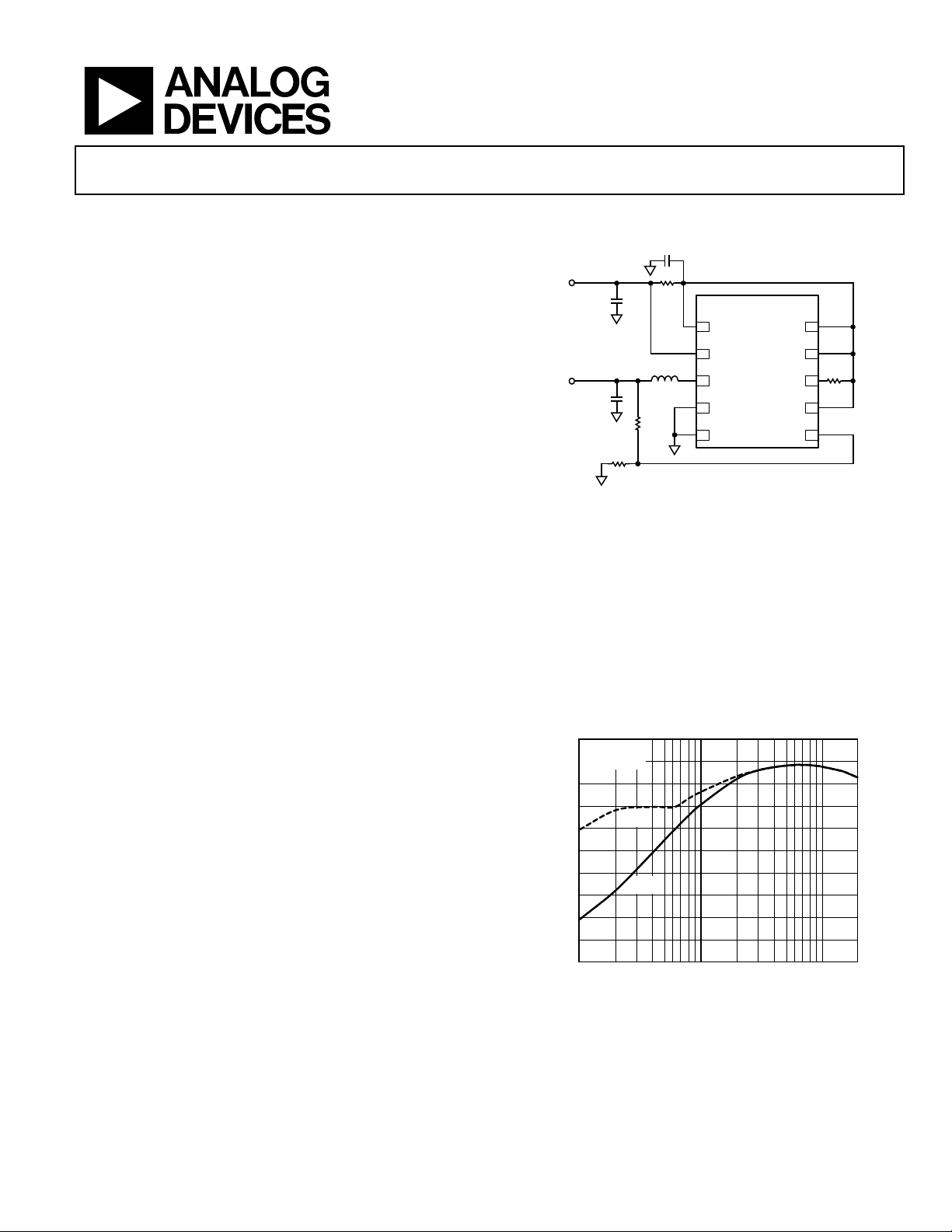
TYPICAL APPLICATION CIRCUIT
C1
0.1µF
V
IN
5V
C
IN
22µF
X5R
6.3V
OUT
3.3V
C
OUT
22µF
X5R
6.3V
R
BOT
2.21kΩ
100
= 5V
V
IN
V
= 1.8V
OUT
90
80
70
60
50
40
EFFICIENCY (%)
30
20
10
0
0.01 0.1 1
Figure 2. ADP2119 Efficiency vs. Output Current
One Technology Way, P.O. Box 9106, Norwood, MA 02062-9106, U.S.A.
Tel: 781.329.4700 www.analog.com
Fax: 781.461.3113 ©2010 Analog Devices, Inc. All rights reserved.
R1
10Ω
L
1.5µH
R
TOP
10kΩ
PFM
FPWM
OUTPUT CURRENT (A)
ADP2119/ADP2120
1
VIN
2
SYNC/MODE
PVIN
3
SW
4
PGND
5
GND
Figure 1.
EN
PGOOD
TRK
FB
10
9
R2
10kΩ
8
7
6
08716-001
08716-002
Page 2

ADP2119/ADP2120
TABLE OF CONTENTS
Features .............................................................................................. 1
Applications ....................................................................................... 1
Typical Application Circuit ............................................................. 1
General Description ......................................................................... 1
Revision History ............................................................................... 2
Specifications ..................................................................................... 3
Absolute Maximum Ratings ............................................................ 5
Thermal Resistance ...................................................................... 5
Boundary Condition .................................................................... 5
ESD Caution .................................................................................. 5
Pin Configuration and Function Descriptions ............................. 6
Typical Performance Characteristics ............................................. 7
Functional Block Diagram ............................................................ 15
Theory of Operation ...................................................................... 16
Control Scheme .......................................................................... 16
PWM Mode Operation .............................................................. 16
PFM Mode Operation ................................................................ 16
Slope Compensation .................................................................. 16
Enable/Shutdown ....................................................................... 16
Integrated Soft Start ................................................................... 16
Tracking ....................................................................................... 17
Oscillator and Synchronization ................................................ 17
Current Limit and Short-Circuit Protection .............................. 17
Overvoltage Protection (OVP) ................................................. 17
Undervoltage Lockout (UVLO) ............................................... 17
Thermal Shutdown .................................................................... 17
Power Good (PGOOD) ............................................................. 17
Applications Information .............................................................. 18
Output Voltage Selection ........................................................... 18
Inductor Selection ...................................................................... 18
Output Capacitor Selection ....................................................... 18
Input Capacitor Selection .......................................................... 19
Voltage Tracking ......................................................................... 19
Typical Application Circuits ......................................................... 20
Outline Dimensions ....................................................................... 22
Ordering Guide .......................................................................... 22
REVISION HISTORY
6/10—Revision 0: Initial Version
Rev. 0 | Page 2 of 24
Page 3

ADP2119/ADP2120
SPECIFICATIONS
VIN = V
Table 1.
Parameter Symbol Test Conditions/Comments Min Typ Max Unit
VIN and PVIN
VIN Voltage Range VIN 2.3 5.5 V
PVIN Voltage Range V
Quiescent Current I
Switching, no load, SYNC/MODE = VIN 680 900 μA
Shutdown Current I
VIN Undervoltage Lockout Threshold UVLO VIN rising 2.2 2.3 V
V
OUTPUT CHARACTERISTICS
Load Regulation1 ADP2119, IO = 0 A to 2 A 0.08 %/A
Load Regulation2 ADP2120, IO = 0 A to 1.25 A 0.08 %/A
Line Regulation1 ADP2119, IO = 1 A 0.05 %/V
Line Regulation2 ADP2120, IO = 1 A 0.05 %/V
FB
FB Regulation Voltage VFB V
FB Bias Current IFB V
SW
High-Side On Resistance3 V
Low-Side On Resistance3 V
SW Peak Current Limit High-side switch, VIN = V
High-side switch, VIN = V
SW Maximum Duty Cycle VIN = V
SW Minimum On Time4 V
TRK
TRK Input Voltage Range 0 600 mV
TRK-to-FB Offset Voltage TRK = 0 mV to 500 mV −15 +15 mV
TRK Input Bias Current 100 nA
FREQUENCY
Oscillator Frequency fS 1.02 1.2 1.38 MHz
SYNC/MODE
Synchronization Range 1 2 MHz
SYNC Minimum Pulse Width 100 ns
SYNC Minimum Off Time 100 ns
SYNC Input High Voltage 1.3 V
SYNC Input Low Voltage 0.4 V
INTEGRATED SOFT START
Soft Start Time All switching frequencies 1024
f
PGOOD
Power-Good Range FB rising threshold 105 110 115 %
FB rising hysteresis 2.5 %
FB falling threshold 85 90 95 %
FB falling hysteresis 2.5 %
Power-Good Deglitch Time From FB to PGOOD 16
PGOOD Leakage Current V
PGOOD Output Low Voltage I
PGOOD Output Low Resistor I
= 3.3 V, EN = VIN, SYNC/MODE = VIN at TJ = −40°C to +125°C, unless otherwise noted.
PVIN
2.3 5.5 V
PVIN
No switching, SYNC/MODE = GND 150 200 μA
VIN
V
SHDN
= V
= 5.5 V, EN = GND 0.3 2 μA
IN
PVIN
falling 2 2.1 V
IN
= 2.3 V to 5.5 V 0.591 0.6 0.609 V
IN
= 2.3 V to 5.5 V 0.01 0.1 μA
IN
= V
= 3.3 V, ISW = 200 mA 145 190 mΩ
IN
PVIN
= V
= 3.3 V, ISW = 200 mA 70 100 mΩ
IN
PVIN
= 3.3 V (ADP2119) 2.5 3 3.5 A
PVIN
= 3.3 V (ADP2120) 1.6 2 2.4 A
PVIN
= 5.5 V, full frequency 100 %
PVIN
= V
= 5.5 V, full frequency 100 ns
IN
PVIN
= 1.2 MHz 853 μs
S
= 5 V 0.1 1 μA
PGOOD
= 1 mA 150 200 mV
PGOOD
= 1 mA 150 200 Ω
PGOOD
Rev. 0 | Page 3 of 24
Clock
cycles
Clock
cycles
Page 4

ADP2119/ADP2120
Parameter Symbol Test Conditions/Comments Min Typ Max Unit
EN
EN Input Rising Threshold VIN = 2.3 V to 5.5 V 1.12 1.2 1.28 V
EN Input Hysteresis VIN = 2.3 V to 5.5 V 100 mV
EN Pull-Down Resistor 1 MΩ
THERMAL
Thermal Shutdown Threshold 150 °C
Thermal Shutdown Hysteresis 25 °C
1
Specified by the circuit in . Figure 54
2
Specified by the circuit in . Figure 58
3
Pin-to-pin measurements.
4
Guaranteed by design.
Rev. 0 | Page 4 of 24
Page 5
ADP2119/ADP2120
ABSOLUTE MAXIMUM RATINGS
Table 2.
Parameter Rating
VIN, PVIN −0.3 V to +6 V
SW −0.3 V to +6 V
FB, SYNC/MODE, EN, TRK, PGOOD −0.3 V to +6 V
PGND to GND −0.3 V to +0.3 V
Operating Junction Temperature Range −40°C to +125°C
Storage Temperature Range −65°C to +150°C
Soldering Conditions JEDEC J-STD-020
Stresses above those listed under Absolute Maximum Ratings
may cause permanent damage to the device. This is a stress
rating only; functional operation of the device at these or any
other conditions above those indicated in the operational
section of this specification is not implied. Exposure to absolute
maximum rating conditions for extended periods may affect
device reliability.
THERMAL RESISTANCE
θJA is specified for the worst-case conditions, that is, a device
soldered in a circuit board for surface-mount packages.
Table 3. Thermal Resistance
Package Type θJA Unit
10-Lead LFCSP_WD 40 °C/W
BOUNDARY CONDITION
θJA is measured using natural convection on a JEDEC 4-layer
board, and the exposed pad is soldered to the printed circuit
board (PCB) with thermal vias.
ESD CAUTION
Rev. 0 | Page 5 of 24
Page 6
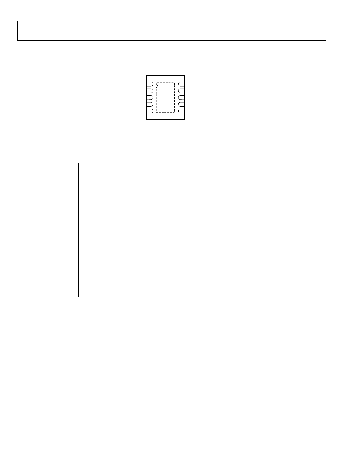
ADP2119/ADP2120
A
PIN CONFIGURATION AND FUNCTION DESCRIPTIONS
DP2119/ADP2120
1
VIN
2
PVIN
3
SW
PGND
GND
NOTES
1. THE EXPOSED PAD SHOULD BE SO LDERED TO
AN EXTERNAL GROUND PLANE UNDERNEAT H
THE IC FOR THERMAL DISSIPATION.
EXPOSED
4
PAD
5
10
EN
9
SYNC/MODE
8
PGOOD
7
TRK
6
FB
08716-003
Figure 3. Pin Configuration (Top View)
Table 4. Pin Function Descriptions
Pin No. Mnemonic Description
1 VIN
Bias Voltage Input Pin. Connect a bypass capacitor (0.1 μF minimum) between this pin and GND and a
small (10 Ω) resistor between this pin and PVIN.
2 PVIN Power Input Pin. Connect this pin to the input power source. Connect a bypass capacitor between this pin and PGND.
3 SW Switch Node Output. Connect this pin to the output inductor.
4 PGND Power Ground. Connect this pin to the power ground plane and to the high current return for the power MOSFET.
5 GND Analog Ground. Connect this pin to the ground plane.
6 FB
7 TRK
Feedback Voltage Sense Input. Connect this pin to a resistor divider from V
connect to V
directly.
OUT
Tracking Input. To track a master voltage, drive TRK from a resistor divider from the master voltage. If the
. For the fixed output version,
OUT
tracking function is not used, connect TRK to VIN.
8 PGOOD Power-Good Output (Open Drain). Connect this pin to a resistor to any pull-up voltage < 5.5 V.
9 SYNC/MODE
Synchronization Input (SYNC). Connect this pin to an external clock between 1 MHz and 2 MHz to synchronize
the switching frequency to the external clock (see the Oscillator and Synchronization section for details).
FPWM/PFM Selection (MODE). When this pin is connected to VIN, the PFM mode is disabled and the part works
in continuous conduction mode (CCM) only. When this pin is connected to ground, the PFM mode is enabled
and becomes active at light loads.
10 EN
Precision Threshold Enable Input Pin. An external resistor divider can be used to set the turn-on threshold. To
enable the part automatically, connect the EN pin to VIN. This pin has a 1 MΩ pull-down resistor to GND.
EPAD Exposed Pad The exposed pad should be soldered to an external ground plane underneath the IC for thermal dissipation.
Rev. 0 | Page 6 of 24
Page 7
ADP2119/ADP2120
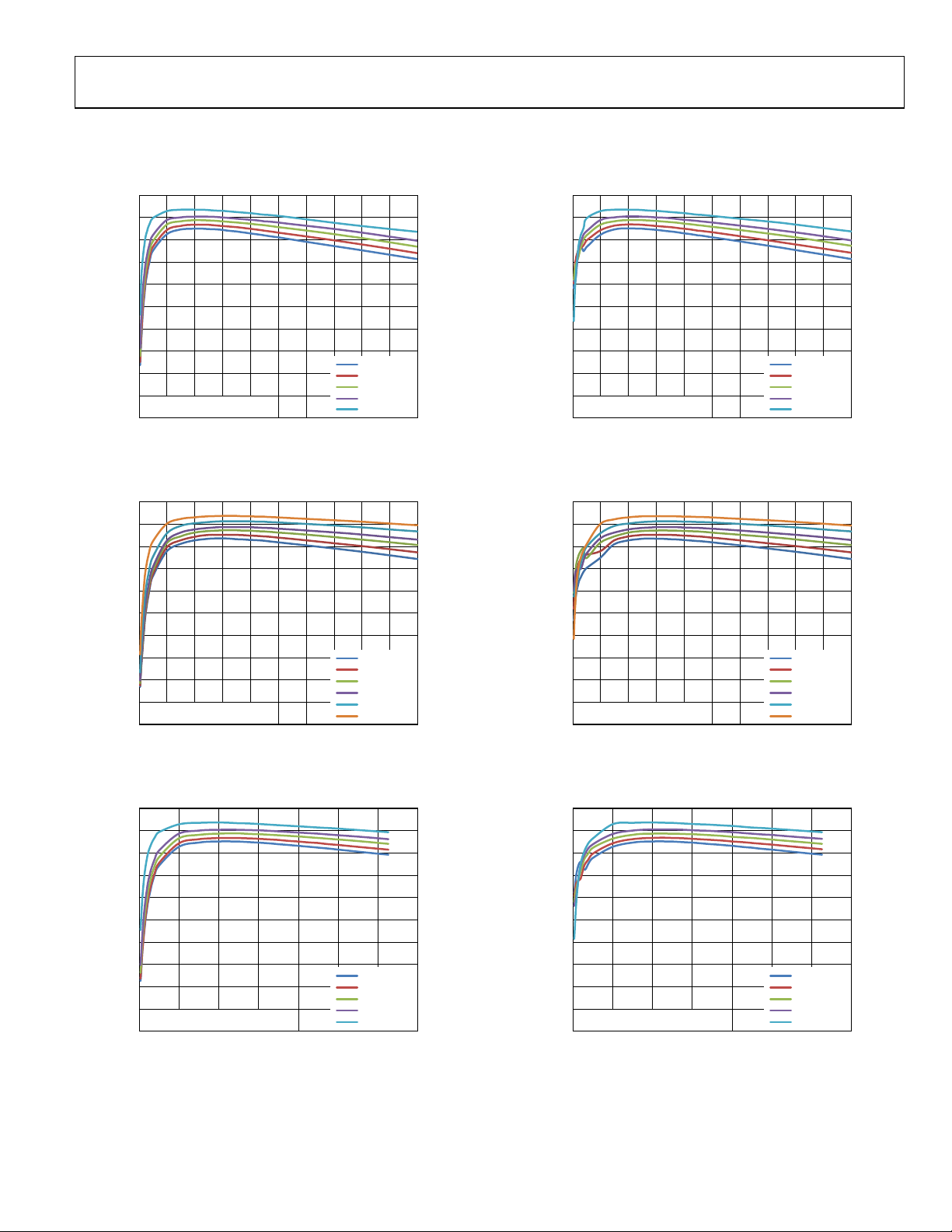
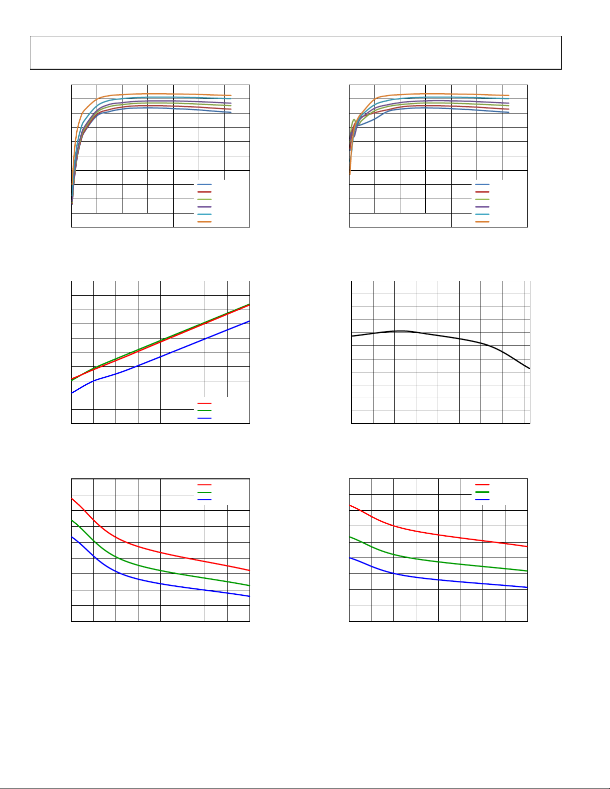
TYPICAL PERFORMANCE CHARACTERISTICS
TA = 25°C, VIN = V
100
90
80
70
60
50
40
EFFICIENCY (%)
30
20
10
INDUCTOR SUMIDA
CDRH5D18BHPNP-1R5M
0
0 0.2 0.4 0.6 0.8 1.0 1.2 1.4 1.6 1.8 2.0
Figure 4. Efficiency (ADP2119, VIN = 3.3 V, FPWM) vs. Output Current
100
90
80
70
60
50
40
EFFICIENCY (%)
30
20
10
INDUCTOR SUMIDA
CDRH5D18BHPNP-1R5M
0
0 0.2 0.4 0.6 0.8 1.0 1.2 1.4 1.6 1.8 2.0
Figure 5. Efficiency (ADP2119, VIN = 5 V, FPWM) vs. Output Current
100
90
80
70
60
50
40
EFFICIENCY (%)
30
20
10
INDUCTOR SUMIDA
CDRH5D18BHPNP-1R5M
0
0 0.2 0.4 0.6 0.8 1.0 1.2 1.4
Figure 6. Efficiency (ADP2120, VIN = 3.3 V, FPWM) vs. Output Current
= 5 V, V
PVIN
OUTPUT CURRENT (A)
OUTPUT CURRENT (A)
OUTPUT CURRENT (A)
= 1.2 V, L = 1.5 μH, CIN = 22 μF, C
OUT
V
= 1.0V
OUT
V
= 1.2V
OUT
V
= 1.5V
OUT
V
= 1.8V
OUT
V
= 2.5V
OUT
V
= 1.0V
OUT
V
= 1.2V
OUT
V
= 1.5V
OUT
V
= 1.8V
OUT
V
= 2.5V
OUT
V
= 3.3V
OUT
V
= 1.0V
OUT
V
= 1.2V
OUT
V
= 1.5V
OUT
V
= 1.8V
OUT
V
= 2.5V
OUT
= 2 × 22 μF, unless otherwise noted.
OUT
100
90
80
70
60
50
40
EFFICIENCY (%)
30
20
10
INDUCTOR SUMIDA
CDRH5D18BHPNP-1R5M
0
0 0.2 0.4 0.6 0.8 1.0 1.2 1.4 1.6 1.8 2.0
08716-004
OUTPUT CURRENT (A)
V
= 1.0V
OUT
V
= 1.2V
OUT
V
= 1.5V
OUT
V
= 1.8V
OUT
V
= 2.5V
OUT
08716-007
Figure 7. Efficiency (ADP2119, VIN = 3.3 V, PFM) vs. Output Current
100
90
80
70
60
50
40
EFFICIENCY (%)
30
20
10
INDUCTOR SUMIDA
CDRH5D18BHPNP-1R5M
0
0 0.2 0.4 0.6 0.8 1.0 1.2 1.4 1.6 1.8 2.0
08716-005
OUTPUT CURRENT (A)
V
= 1.0V
OUT
V
= 1.2V
OUT
V
= 1.5V
OUT
V
= 1.8V
OUT
V
= 2.5V
OUT
V
= 3.3V
OUT
08716-008
Figure 8. Efficiency (ADP2119, VIN = 5 V, PFM) vs. Output Current
100
90
80
70
60
50
40
EFFICIENCY (%)
30
20
10
INDUCTOR SUMIDA
CDRH5D18BHPNP-1R5M
0
0 0.2 0.4 0.6 0.8 1.0 1.2 1.4
08716-006
OUTPUT CURRENT (A)
V
= 1.0V
OUT
V
= 1.2V
OUT
V
= 1.5V
OUT
V
= 1.8V
OUT
V
= 2.5V
OUT
08716-009
Figure 9. Efficiency (ADP2120, VIN = 3.3 V, PFM) vs. Output Current
Rev. 0 | Page 7 of 24
Page 8
ADP2119/ADP2120
100
90
80
70
60
50
40
EFFICIENCY (%)
30
20
10
INDUCTOR SUMIDA
CDRH5D18BHPNP-1R5M
0
0 0.2 0.4 0.6 0.8 1.0 1.2 1.4
OUTPUT CURRENT (A)
V
= 1.0V
OUT
V
= 1.2V
OUT
V
= 1.5V
OUT
V
= 1.8V
OUT
V
= 2.5V
OUT
V
= 3.3V
OUT
Figure 10. Efficiency (ADP2120, VIN = 5 V, FPWM) vs. Output Current
900
850
800
750
700
650
600
550
QUIESCENT CURRENT (µ A)
500
450
400
2.3 5.55.14.74.33.93.53.12.7
VIN (V)
TJ = +125°C
TJ = +25°C
TJ = –40°C
Figure 11. Quiescent Current vs. VIN (Switching)
275
250
225
200
175
150
125
PFET RESISTO R ( mΩ)
100
75
50
2.3 5.55.14.74.33.93.53.12.7
VIN (V)
TJ = +125°C
TJ = +25°C
TJ = –40°C
Figure 12. PFET Resistor vs. VIN (Pin-to-Pin Measurements)
08716-010
08716-011
08716-012
100
90
80
70
60
50
40
EFFICIENCY (%)
30
20
10
INDUCTOR SUMIDA
CDRH5D18BHPNP-1R5M
0
0 0.2 0.4 0.6 0.8 1.0 1.2 1.4
OUTPUT CURRENT (A)
V
= 1.0V
OUT
V
= 1.2V
OUT
V
= 1.5V
OUT
V
= 1.8V
OUT
V
= 2.5V
OUT
V
= 3.3V
OUT
Figure 13. Efficiency (ADP2120, VIN = 5 V, PFM) vs. Output Current
605
604
603
602
601
600
599
598
597
FEEDBACK VOLTAGE (mV)
596
595
594
–40 120100806040200–20
TEMPERATURE (°C)
Figure 14. Feedback Voltage vs. Temperature (VIN = 3.3 V)
120
110
100
90
80
70
60
NFET RESIS TOR (mΩ)
50
40
30
2.3 5.55.14.74.33.93.53.12.7
VIN (V)
TJ = +125°C
TJ = +25°C
TJ = –40°C
Figure 15. NFET Resistor vs. VIN (Pin-to-Pin Measurements)
08716-013
08716-014
08716-015
Rev. 0 | Page 8 of 24
Page 9

ADP2119/ADP2120
1.30
2.30
1.25
1.20
1.15
1.10
EN THRESHOLD ( V )
1.05
1.00
3.1
3.0
2.9
2.8
2.7
PEAK CURRENT LIM IT (A)
2.6
RISING
FALLING
–40 120100806040200–20
TEMPERATURE (°C)
Figure 16. EN Threshold vs. Temperature
2.25
RISING
2.20
2.15
2.10
UVLO THRESHOLD (V)
2.05
2.00
–40 120100806040200–20
08716-016
FALLING
TEMPERATURE (°C)
08716-019
Figure 19. UVLO Threshold vs. Temperature (VIN = 3.3 V)
3.5
3.3
3.1
2.9
2.7
2.5
PEAK CURRENT LIM IT (A)
2.3
TJ = +125°C
TJ = +25°C
TJ = –40°C
2.5
–40 120100806040200–20
TEMPERATURE (°C)
Figure 17. Peak Current Limit vs. Temperature (ADP2119, VIN = 3.3 V)
2.10
2.05
2.00
1.95
1.90
1.85
PEAK CURRENT LIM IT (A)
1.80
1.75
–40 120100806040200–20
TEMPERATURE (°C)
Figure 18. Peak Current Limit vs. Temperature (ADP2120, V
= 3.3 V)
IN
2.1
2.3 5.55.14.74.33.93.53.12.7
08716-017
VIN (V)
08716-020
Figure 20. Peak Current Limit vs. VIN (ADP2119)
2.2
2.1
2.0
1.9
1.8
PEAK CURRENT LIMIT (A)
1.7
1.6
2.3 5.55.14.74.33.93.53.12.7
08716-018
VIN (V)
TJ = +125°C
TJ = +25°C
TJ = –40°C
08716-021
Figure 21. Peak Current Limit vs. VIN (ADP2120)
Rev. 0 | Page 9 of 24
Page 10

ADP2119/ADP2120
T
T
3
1
2
4
CH1 500mV CH2 5.00V
CH3 5.00V CH4 2.00A Ω
EN
V
OUT
PGOOD
I
L
M400µs A CH3 3.60V
T 30.4%
Figure 22. Soft Start with Full Load (ADP2119, VIN = 5 V)
T
V
(AC)
1
4
OUT
I
O
3
1
2
4
CH1 500mV CH2 5.00V
08716-022
CH3 5.00V CH4 2.00A Ω
EN
V
OUT
PGOOD
I
L
M400µs A CH3 3.50V
T 784.0µs
08716-025
Figure 25. Soft Start with Precharged Output (ADP2119, VIN = 5 V)
T
V
(AC)
1
4
OUT
I
O
CH1 50.0mV
CH4 1.00A Ω
M200µs A CH4 880mA
T 596.0µs
Figure 23. Load Transient (ADP2119, PFM, VIN = 5 V)
T
V
(AC)
1
4
CH1 50.0mV
CH4 1.00A Ω
OUT
I
O
M200µs A CH4 960mA
T 396.0µs
Figure 24. Load Transient (ADP2120, PFM, VIN = 5 V)
CH1 50.0mV
08716-023
CH4 1.00A Ω
M200µs A CH4 880mA
T 596.0µs
08716-026
Figure 26. Load Transient (ADP2119, FPWM, VIN = 5 V)
T
V
(AC)
1
4
CH1 50.0mV
08716-024
CH4 1.00A Ω
OUT
I
O
M200µs A CH4 960mA
T 396.0µs
08716-027
Figure 27. Load Transient (ADP2120, FPWM, VIN = 5 V)
Rev. 0 | Page 10 of 24
Page 11

ADP2119/ADP2120
T
V
OUT
V
1
SW
OUT
1
T
2
I
4
CH1 500mV CH2 5.00V
L
CH4 2.00A Ω
Figure 28. Output Short (ADP2119)
V
OUT
1
SW
2
I
4
CH1 500mV CH2 5.00V
L
CH4 2.00A Ω
Figure 29. Output Short (ADP2120)
SW
2
I
L
4
M2.0ms A CH1 480mV
T 3.92ms
08716-028
CH1 500mV CH2 5.00V
CH4 2.00A Ω
M2.0ms A CH1 560mV
T –2.08ms
08716-031
Figure 31. Output Short Recovery (ADP2119)
T
V
OUT
1
SW
2
I
L
4
M2.0ms A CH1 200mV
T 3.96ms
08716-029
CH1 500mV CH2 5.00V
CH4 2.00A Ω
T
M2.0ms A CH1 560mV
T –2.12ms
08716-032
Figure 32. Output Short Recovery (ADP2120)
T
TRK
FB
1
CH1 500mV CH2 500mV M2.0ms A CH2 730mV
T 44.4%
Figure 30. Tracking Function
08716-030
Rev. 0 | Page 11 of 24
T
SYNC
1
2
SW
CH1 2.0V CH2 2.0V M400n s A CH1 4.12V
T 0.0s
Figure 33. Synchronized to 1 MHz
08716-033
Page 12

ADP2119/ADP2120
V
(AC)
1
2
4
OUT
SW
I
L
CH1 20.0mV CH2 5.00V
CH4 500mA Ω
T
M4.0µs A CH4 820mA
T –40.0ns
Figure 34. PFM Mode
V
(AC)
1
2
4
OUT
SW
I
L
CH1 5.0mV CH2 5.00V
CH4 500mA Ω
T
M1.0µs A CH2 4.3V
T –40.0ns
Figure 35. Discontinuous Conduction Mode (DCM)
V
(AC)
1
2
4
OUT
SW
I
L
CH1 5.0mV CH2 5.00V
CH4 1.0A Ω
T
M1.0µs A CH2 4.3V
T –40.0ns
Figure 36. Continuous Conduction Mode (CCM)
80
64
48
32
16
0
–16
MAGNITUDE (dB)
–32
–48
–64
CROSS FREQ UE NCY : 124k Hz
PHASE MARGIN: 46°
–80
08716-034
08716-035
08716-036
1k 10k 100k 1M
FREQUENCY (Hz)
Figure 37. ADP2119 Bode Plot at VIN = 5 V, V
L = 1 μH, C
80
64
48
32
16
0
–16
MAGNITUDE (dB)
–32
–48
–64
CROSS FREQ UE NCY : 105k Hz
PHASE MARGIN: 47°
–80
1k 10k 100k 1M
FREQUENCY (Hz)
= 2 × 22 μF
OUT
Figure 38. ADP2119 Bode Plot at VIN = 5 V, V
L = 1.5 μH, C
80
64
48
32
16
0
–16
MAGNITUDE (dB)
–32
–48
–64
CROSS FREQ UE NCY : 112k Hz
PHASE MARGIN: 48°
–80
1k 10k 100k 1M
FREQUENCY (Hz)
= 2 × 22 μF
OUT
Figure 39. ADP2119 Bode Plot at VIN = 5 V, V
L = 1.5 μH, C
= 22 μF +10 μF
OUT
= 1.0 V, IO = 2 A,
OUT
= 1.2 V, IO = 2 A,
OUT
= 1.5 V, IO = 2 A,
OUT
200
160
120
80
40
0
–40
–80
–120
–160
–200
200
160
120
80
40
0
–40
–80
–120
–160
–200
200
160
120
80
40
0
–40
–80
–120
–160
–200
PHASE (Degrees)
08716-037
PHASE (Degrees)
08716-038
PHASE (Degrees)
08716-039
Rev. 0 | Page 12 of 24
Page 13

ADP2119/ADP2120
80
64
48
32
16
0
–16
MAGNITUDE (dB)
–32
–48
–64
CROSS FREQ UENCY: 99kHz
PHASE MARGIN: 52°
–80
1k 10k 100k 1M
FREQUENCY (Hz)
Figure 40. ADP2119 Bode Plot at VIN = 5 V, V
L = 1.5 μH, C
80
64
48
32
16
0
–16
MAGNITUDE (dB)
–32
–48
–64
CROSS FREQ UE NCY : 107k Hz
PHASE MARGIN: 49°
–80
1k 10k 100k 1M
= 22 μF + 10 μF
OUT
FREQUENCY (Hz)
Figure 41. ADP2119 Bode Plot at VIN = 5 V, V
L = 1.5 μH, C
80
64
48
32
16
0
–16
MAGNITUDE (dB)
–32
–48
–64
CROSS FREQ UENCY: 89kHz
PHASE MARGIN: 58°
–80
1k 10k 100k 1M
FREQUENCY (Hz)
= 22 μF
OUT
Figure 42. ADP2119 Bode Plot at VIN = 5 V, V
L = 1.5 μH, C
= 22 μF
OUT
= 1.8 V, IO = 2 A,
OUT
= 2.5 V, IO = 2 A,
OUT
= 3.3 V, IO = 2 A,
OUT
200
160
120
80
40
0
–40
–80
–120
–160
–200
200
160
120
80
40
0
–40
–80
–120
–160
–200
200
160
120
80
40
0
–40
–80
–120
–160
–200
PHASE (Degrees)
08716-040
PHASE (Degrees)
08716-041
PHASE (Degrees)
08716-042
80
64
48
32
16
0
–16
MAGNITUDE (dB)
–32
–48
–64
CROSS FREQ UENCY: 87kHz
PHASE MARGIN: 48°
–80
1k 10k 100k 1M
FREQUENCY (Hz)
Figure 43. ADP2120 Bode Plot at VIN = 5 V, V
L = 1.5 μH, C
80
64
48
32
16
0
–16
MAGNITUDE (dB)
–32
–48
–64
CROSS FREQ UENCY: 80kHz
PHASE MARGIN: 54°
–80
1k 10k 100k 1M
= 22 μF + 10 μF
OUT
FREQUENCY (Hz)
Figure 44. ADP2120 Bode Plot at VIN = 5 V, V
L = 1.5 μH, C
80
64
48
32
16
0
–16
MAGNITUDE (dB)
–32
–48
–64
CROSS FREQ UENCY: 67kHz
PHASE MARGIN: 51°
–80
1k 10k 100k 1M
= 22 μF + 10 μF
OUT
FREQUENCY (Hz)
Figure 45. ADP2120 Bode Plot at VIN = 5 V, V
L = 2.2 μH, C
= 22 μF + 10 μF
OUT
= 1.0 V, IO = 1.25 A,
OUT
= 1.2 V, IO = 1.25 A,
OUT
= 1.5 V, IO = 1.25 A,
OUT
200
160
120
80
40
0
–40
–80
–120
–160
–200
200
160
120
80
40
0
–40
–80
–120
–160
–200
200
160
120
80
40
0
–40
–80
–120
–160
–200
PHASE (Degrees)
PHASE (Degrees)
PHASE (Degrees)
08716-043
08716-044
08716-045
Rev. 0 | Page 13 of 24
Page 14

ADP2119/ADP2120
80
64
48
32
16
0
–16
MAGNITUDE (dB)
–32
–48
–64
CROSS FREQ UENCY: 78kHz
PHASE MARGIN: 50°
–80
1k 10k 100k 1M
FREQUENCY (Hz)
Figure 46. ADP2120 Bode Plot at VIN = 5 V, V
L = 2.2 μH, C
80
64
48
32
16
0
–16
MAGNITUDE (dB)
–32
–48
–64
CROSS FREQ UENCY: 61kHz
PHASE MARGIN: 54°
–80
1k 10k 100k 1M
FREQUENCY (Hz)
= 2 ×10 μF
OUT
Figure 47. ADP2120 Bode Plot at VIN = 5 V, V
L = 2.2 μH, C
= 2 ×10 μF
OUT
= 1.8 V, IO = 1.25 A,
OUT
= 2.5 V, IO = 1.25 A,
OUT
200
160
120
80
40
0
–40
–80
–120
–160
–200
200
160
120
80
40
0
–40
–80
–120
–160
–200
PHASE (Degrees)
08716-046
PHASE (Degrees)
08716-047
80
64
48
32
16
0
–16
MAGNITUDE (dB)
–32
–48
–64
CROSS FREQ UENCY: 48kHz
PHASE MARGIN: 60°
–80
1k 10k 100k 1M
FREQUENCY (Hz)
Figure 48. ADP2120 Bode Plot at VIN = 5 V, V
L = 2.2 μH, C
= 2 ×10 μF
OUT
= 3.3 V, IO = 1.25 A,
OUT
200
160
120
80
40
0
–40
–80
–120
–160
–200
PHASE (Degrees)
08716-048
Rev. 0 | Page 14 of 24
Page 15

ADP2119/ADP2120
V
FUNCTIONAL BLOCK DIAGRAM
IN
EN
PVIN
TRK
PGOOD
GND
FB
ADP2119/
ADP2120
0.6V
SOFT
START
0.66V
0.54V
ERROR
AMPLIFIER
Gm
SKIP MODE
THRESHOLD
Z
COMP
UVLO
SKIP
COMPARATOR
COMPENSATION
SYNC/MODE
PWM AND
PROTECTION
LOGIC
CONTROL
SLOPE
OSCILLATOR
CLK
PMOS CURRENT
SENSE AMPLIFIER
NMOS
CURRENT
SENSE
AMPLIFIER
ZERO-CROSSING
COMPARATOR
PFET
NFET
SW
PGND
08716-049
Figure 49. Functional Block Diagram
Rev. 0 | Page 15 of 24
Page 16

ADP2119/ADP2120
THEORY OF OPERATION
The ADP2119/ADP2120 are step-down, dc-to-dc regulators
that use a fixed frequency, peak current mode architecture with
integrated high-side switch and low-side synchronous rectifier.
The high switching frequency and tiny 10-lead, 3 mm × 3 mm
LFCSP_WD package provide a small step-down dc-to-dc regulator
solution. The integrated high-side switch (P-channel MOSFET)
and synchronous rectifier (N-channel MOSFET) yield high
efficiency at medium-to-full loads while light load efficiency
is improved using the PFM mode.
The ADP2119/ADP2120 support input voltages from 2.3 V
to 5.5 V and regulate the output voltage down to 0.6 V. The
ADP2119/ADP2120 are also available with preset output
voltage options of 3.3 V, 2.5 V, 1.8 V, 1.5 V, 1.2 V, and 1.0 V.
CONTROL SCHEME
The ADP2119/ADP2120 use a fixed frequency, peak current
mode PWM control architecture and operate in PWM mode
for medium-to-full loads but shift to PFM mode (if enabled) at
light loads to maintain high efficiency. When operating in fixed
frequency PWM mode, the duty cycle of the integrated switches
is adjusted to regulate the output voltage. When operating in
PFM mode at light loads, the switching frequency is adjusted
to regulate the output voltage.
The ADP2119/ADP2120 operate in PWM mode when the load
current is greater than the pulse-skipping threshold current. At
load currents below this value, the regulator smoothly transitions
to the PFM mode of operation.
PWM MODE OPERATION
In PWM mode, the ADP2119/ADP2120 operate at a fixed
frequency. At the start of each oscillator cycle, the P-channel
MOSFET switch is turned on, putting a positive voltage across
the inductor. Current in the inductor increases until the current
sense signal crosses the peak inductor current level, turns off
the P-channel MOSFET switch, and turns on the N-channel
MOSFET synchronous rectifier. This puts a negative voltage
across the inductor, causing the inductor current to decrease.
The synchronous rectifier stays on for the rest of the cycle or
until the inductor current reaches zero, which causes the zerocrossing comparator to turn off the N-channel MOSFET as well.
The peak inductor current level is set by V
of a transconductance error amplifier that compares the feedback
voltage with an internal 0.6 V reference.
COMP
. V
COMP
is the output
PFM MODE OPERATION
When PFM mode is enabled, the regulator smoothly transitions
to the variable frequency PFM mode of operation when the load
current decreases below the pulse-skipping threshold current.
Switching continues only as necessary to maintain the output
voltage within regulation. When the output voltage drops below
regulation, the part enters PWM mode for a few oscillator cycles to
increase the output voltage back to regulation. During the wait
time between bursts, both power switches are off, and the output
capacitor supplies the load current. Because the output voltage
dips and recovers occasionally, the output voltage ripple in this
mode is larger than the ripple in the PWM mode of operation.
SLOPE COMPENSATION
Slope compensation stabilizes the internal current control loop
of the ADP2119/ADP2120 when operating close to and beyond
the 50% duty cycle to prevent subharmonic oscillations. Slope
compensation is implemented by summing an artificial voltage
ramp to the current sense signal during the on-time of the P-channel
MOSFET switch. This voltage ramp depends on the output voltage.
When operating at high output voltages, there is more slope
compensation. The slope compensation ramp value determines
the minimum inductor that can be used to prevent subharmonic
oscillations.
ENABLE/SHUTDOWN
The EN input pin has a precision analog threshold of 1.2 V (typical)
with 100 mV of hysteresis. When the enable voltage exceeds 1.2 V,
the regulator turns on, and when it falls below 1.1 V (typical),
the regulator turns off. To force the part to automatically start
when input power is applied, connect EN to VIN.
When the ADP2119/ADP2120 are shut down, the soft start
capacitor is discharged. This causes a new soft start cycle to
begin when the part is reenabled.
An internal pull-down resistor (1 MΩ) prevents an accidental
enable if EN is left floating.
INTEGRATED SOFT START
The ADP2119/ADP2120 include integrated soft start circuitry
to limit the output voltage rise time and reduce inrush current
at startup. The soft start time is fixed at 1024 clock cycles.
If the output voltage is precharged prior to turn-on, the part
prevents reverse inductor current (which would discharge the
output capacitor) by keeping both MOSFETs turned off until
the soft start voltage exceeds the voltage on the FB pin.
Rev. 0 | Page 16 of 24
Page 17

ADP2119/ADP2120
TRACKING
The ADP2119/ADP2120 have a tracking input, TRK, that allows
the output voltage to track another voltage (master voltage).
The tracking input is especially useful in core and I/O voltage
tracking for FPGAs, DSPs, and ASICs.
The internal error amplifier includes three positive inputs: the
internal reference voltage, the soft start voltage, and the TRK
voltage. The error amplifier regulates the FB voltage to the
lowest of the three voltages. To track a master voltage, tie the
TRK pin to a resistor divider from the master voltage. If the
tracking function is not used, connect the TRK pin to VIN.
OSCILLATOR AND SYNCHRONIZATION
To synchronize the ADP2119/ADP2120, drive an external clock
at the SYNC/MODE pin. The frequency of the external clock
can be in the 1 MHz to 2 MHz range. During synchronization,
the regulator operates in CCM mode only, and the switching
frequency is in phase with the external clock.
CURRENT LIMIT AND SHORT-CIRCUIT PROTECTION
The ADP2119/ADP2120 have a peak current limit protection
circuit to prevent current runaway. When the inductor peak
current reaches the current limit value, the high-side MOSFET
turns off and the low-side MOSFET turns on until the next cycle
starts. The overcurrent counter increments during this time. If
the overcurrent counter count exceeds 10, the part enters hiccup
mode and both the high-side MOSFET and low-side MOSFET
are turned off. The part remains in this mode for 4096 clock cycles
and then attempts to restart from soft start. If the current limit
fault has cleared, the part resumes normal operation. Otherwise,
it reenters hiccup mode again after counting 10 current limit
violations.
OVERVOLTAGE PROTECTION (OVP)
The output voltage is continuously monitored by a comparator
through the FB pin, which is at 0.6 V (typical) under normal
operation. This comparator is set to activate when the FB voltage
exceeds 0.66 V (typical), thus indicating an output overvoltage
condition. If the voltage remains above this threshold for 16
clock cycles, the high-side MOSFET turns off and the low-side
MOSFET turns on until the current through the low-side MOSFET
reaches the limit (−0.6 A for forced continuous conduction mode
and 0 A for PFM mode). Thereafter, both the MOSFETs are
held in the off state until FB falls below 0.54 V (typical), at this
point, the part restarts. The behavior of PGOOD under this
condition is described in the Power Good section.
UNDERVOLTAGE LOCKOUT (UVLO)
Undervoltage lockout circuitry is integrated in the ADP2119/
ADP2120. If the input voltage drops below 2.1 V, the part shuts
down and both the power switch and synchronous rectifier turn
off. When the voltage rises again above 2.2 V, the soft start period is
initiated, and the part is enabled.
THERMAL SHUTDOWN
If the ADP2119/ADP2120 junction temperatures rise above 150°C,
the thermal shutdown circuit turns off the regulators. Extreme
junction temperatures can be the result of high current operation,
poor circuit board design, and/or high ambient temperature. A
25°C hysteresis is included so that if thermal shutdown occurs, the
part does not return to operation until the on-chip temperature
drops below 125°C. When coming out of thermal shutdown,
soft start is initiated.
POWER GOOD (PGOOD)
PGOOD is an active high, open-drain output and requires a
resistor to pull it up to a voltage. A high indicates that the voltage
on the FB pin (and therefore the output voltage) is within ±10%
of the desired value. A low on this pin indicates that the voltage
on the FB pin is not within ±10% of the desired value. There is a
16 cycle waiting period after FB is detected as being out of bounds.
Rev. 0 | Page 17 of 24
Page 18

ADP2119/ADP2120
V
(
)
APPLICATIONS INFORMATION
This section describes the selection of the external components
for the ADP2119/ADP2120. The typical application circuit for
the ADP2119 is shown in Figure 50.
C1
0.1µF
V
IN
5V
OUT
2.5V
C
IN
22µF
X5R
6.3V
C
OUT
2A
22µF
X5R
6.3V
R
BOT
15kΩ
R1
10Ω
L
1.5µH
R
TOP
47.5kΩ
Figure 50. Typical Application Circuit
1
2
3
4
5
ADP2119
VIN
PVIN
SW
PGND
GND
SYNC/MODE
PGOOD
TRK
EN
FB
10
9
R2
10kΩ
8
7
6
08716-050
OUTPUT VOLTAGE SELECTION
The output voltage of the adjustable version can be set by an
external resistive voltage divider, and the following equation
calculates the output voltage.
R
V +×=
OUT
TOP
)(10.6
R
BOT
To limit the output voltage accuracy degradation due to FB bias
current (0.1 μA maximum) to less than 0.5% (maximum), ensure
that R
is less than 30 kΩ.
BOT
INDUCTOR SELECTION
The inductor value is determined by the operating frequency,
input voltage, output voltage, and ripple current. A small inductor
value leads to a larger inductor current ripple and provides a
faster transient response; however, it degrades efficiency. A
large inductor value leads to a smaller current ripple and good
efficiency but slows the transient response. As a guideline, the
inductor current ripple, ΔI
load current trade-off between the transient response and efficiency.
The inductor value can be calculated using the following equation:
IN
L
=
OUT
×
Δ
L
where:
V
is the input voltage.
IN
is the output voltage.
V
OUT
ΔI
is the inductor current ripple.
L
D is the duty cycle. D = V
The regulator uses slope compensation in the current loop to
prevent subharmonic oscillations when the duty cycle is larger
than 50%. The internal slope compensation limits the minimum
inductor value.
, is typically set to 1/3 of the maximum
L
DVV
×−
fI
S
.
OUT/VIN
The negative current limit (−0.6 A) also limits the minimum
inductor value. The inductor current ripple (ΔI
) calculated
L
by the selected inductor should not exceed 1.2 A.
The peak inductor current should be kept below the peak current
limit threshold value and can be calculated from
IIIΔ
L
+=
OPEAK
2
Ensure that the rms current of the selected inductor is greater
than the maximum load current and that its saturation current
is greater than the peak current limit of the regulator.
OUTPUT CAPACITOR SELECTION
The output voltage ripple, load step transient, and loop stability
determine the output capacitor selection.
The ESR and the capacitance determine the output ripple.
⎛
⎜
ESRIV
OUT
L
+×Δ=Δ
⎜
⎝
8
OUT
The load transient response depends on the inductor, the output
capacitor, and the control loop.
The ADP2119/ADP2120 have integrated loop compensation to
provide a simple power solution design. Table 5 and Ta b le 6 show
the typical recommended inductors and capacitors for the ADP2119/
ADP2120. X5R or X7R ceramic capacitors are highly recommended.
Table 5. Recommended L and C
VIN (V) V
(V) L (μH) C
OUT
3.3 1.0 1 22 + 22
3.3 1.2 1 22 + 22
3.3 1.5 1 22 + 10
3.3 1.8 1 22
3.3 2.5 1 22
5 1.0 1 22 + 22
5 1.2 1.5 22 + 22
5 1.5 1.5 22 +10
5 1.8 1.5 22 +10
5 2.5 1.5 22
5 3.3 1.5 22
Table 6. Recommended L and C
VIN (V) V
(V) L (μH) C
OUT
3.3 1.0 1.5 22 + 10
3.3 1.2 1.5 22 + 10
3.3 1.5 1.5 22 + 10
3.3 1.8 1.5 10 + 10
3.3 2.5 1.5 10 + 10
5 1.0 1.5 22 + 10
5 1.2 1.5 22 + 10
5 1.5 2.2 22 + 10
5 1.8 2.2 10 + 10
5 2.5 2.2 10 + 10
5 3.3 2.2 10 + 10
⎞
1
⎟
⎟
fC
××
S
⎠
Values for the ADP2119
OUT
(μF)
OUT
Values for the ADP2120
OUT
(μF)
OUT
Rev. 0 | Page 18 of 24
Page 19

ADP2119/ADP2120
V
V
Higher or lower inductor and output capacitor values can be
used in the regulator, but the system stability and load transient
performance need to be checked. The minimum output capacitor
is 22 μF for the ADP2119 and 10 μF for the ADP2120, and the
inductor range is 1 μH to 3.3 μH.
A common application is coincident tracking (see Figure 52).
Coincident tracking limits the slave output voltage to be the
same as the master voltage until it reaches regulation. Connect
the TRK pin to a resistor divider from the master voltage. For
= R
coincident tracking, set R
TRKT
TOP
and R
TRKB
= R
BOT
.
Table 7. Recommended Inductors
Manufacturer Part Number
Sumida CDRH5D18BHPNP, CDR6D23MNNP
TOKO DE4518C, D62LCB
Coilcraft LPS5030, LPS5015
Table 8. Recommended Capacitors
Manufacturer Part Number Description
Murata GRM31CR60J226KE19 22 μF, 6.3 V, X5R, 1206
Murata GRM319R60J106KE19 10 μF, 6.3 V, X5R, 1206
TDK C3216X5R0J226M 22 μF, 6.3 V, X5R, 1206
TDK C3216X5R0J106M 10 μF, 6.3 V, X5R, 1206
INPUT CAPACITOR SELECTION
The input capacitor reduces the input voltage ripple caused by the
switch current on PVIN. Place the input capacitor as close as
possible to the PVIN pin. A 10 μF or 22 μF ceramic capacitor is
recommended. The rms current rating of the input capacitor
should be larger than calculated by the following equation:
)1( DDII
−××=
ORMS
VOLTAGE TRACKING
The ADP2119/ADP2120 include a tracking feature that allows
the output (slave voltage) to be configured to track an external
voltage (master voltage), as shown in Figure 51.
MASTER
ADP2119/
ADP2120
R
TRKT
TRK
R
TRKB
Figure 51. Voltage Tracking
FB
V
SLAVE
R
TOP
R
BOT
08716-051
V
MASTER
V
SLAVE
VOLTAGE
TIME
8716-052
Figure 52. Coincident Tracking
Ratiometric tracking is shown in Figure 53. The slave output is
limited to a fraction of the master voltage. In this application,
the slave and master voltages reach the final value at the same
time. The ratio of the slave output voltage to the master voltage
is a function of the two dividers (see the following equation).
R
TOP
1
+
V
V
MASTER
SLAVE
VOLTAGE
R
BOT
R
R
TRKT
TRKB
MASTER
V
SLAVE
TIME
08716-053
=
+
1
Figure 53. Ratiometric Tracking
Rev. 0 | Page 19 of 24
Page 20

ADP2119/ADP2120
V
A
V
A
TYPICAL APPLICATION CIRCUITS
C1
0.1µF
V
IN
5V
C
22µF
X5R
6.3V
IN
R1
10Ω
1
VIN
ADP2119
EN
10
OUT
1.2V
2A
L: CDRH5D18BHPNP-1R5M SUMI D
CIN, C
OUT1
C
C
OUT2
OUT1
22µF
22µF
X5R
X5R
6.3V
6.3V
R
BOT
10kΩ
, C
: GRM31CR60J226KE19 MURATA
OUT2
R
TOP
10kΩ
L
1.5µH
2
3
4
5
PVIN
SW
PGND
GND
SYNC/MODE
PGOOD
TRK
FB
9
R2
10kΩ
8
7
6
08716-054
Figure 54. 1.2 V, 2 A, Step-Down Regulator, Forced Continuous Conduction Mode (ADP2119)
C1
0.1µF
V
IN
OUT
1.8V
2A
5V
C
OUT1
10µF
X5R
6.3V
C
C
22µF
X5R
6.3V
OUT2
22µF
X5R
6.3V
R
TOP
20kΩ
R1
10Ω
L
1.5µH
1
2
3
4
5
VIN
PVIN
SW
PGND
GND
ADP2119
SYNC/MODE
PGOOD
EN
TRK
FB
10
9
8
R2
10kΩ
7
6
IN
R
BOT
10kΩ
L: CDRH5D18BHPNP-1R5M SUMI D
CIN, C
C
: GRM31CR60J226KE19 MURATA
OUT2
: GRM319R60J106KE19 MURATA
OUT1
08716-055
Figure 55. 1.8 V, 2 A, Step-Down Regulator, Enable PFM Mode (ADP2119)
Rev. 0 | Page 20 of 24
Page 21

ADP2119/ADP2120
V
A
A
V
IN
5V
OUT
2.5V
2A
L: CDRH5D18BHPNP-1R5M SUMI D
CIN, C
: GRM31CR60J226KE19 MU RATA
OUT
22µF
X5R
6.3V
C
OUT
22µF
X5R
6.3V
C
IN
R
BOT
15kΩ
0.1µF
10Ω
1.5µH
R
TOP
47.5kΩ
C1
R1
ADP2119
1
VIN
2
SYNC/MODE
PVIN
3
4
5
SW
PGND
GND
L
EN
PGOOD
TRK
FB
10
9
10kΩ
8
7
6
EXTERNAL
CLOCK
R2
08716-056
Figure 56. 2.5 V, 2 A, Step-Down Regulator, Synchronized to External Clock (ADP2119)
C1
0.1µF
V
IN
5V
C
22µF
X5R
6.3V
IN
R1
10Ω
1
ADP2120
VIN
EN
10
V
OUT
1.5V
1.25A
L: LPS503 0- 222MLB COILCRAFT
C
, C
IN
OUT1
: GRM319R60J106KE19 MURATA
C
OUT2
C
C
OUT1
22µF
X5R
6.3V
OUT2
10µF
X5R
6.3V
R
BOT
10kΩ
: GRM31CR60J226KE19 MURATA
Figure 57. 1.5 V, 1.25 A, Step-Down Regulator, Tracking Mode (ADP2120)
V
IN
5V
V
OUT
1.25
1.2V
C
OUT1
22µF
X5R
6.3V
C
C
22µF
X5R
6.3V
OUT2
10µF
X5R
6.3V
R
TOP
15kΩ
IN
L
2.2µH
R
BOT
10kΩ
R
TOP
10kΩ
2
3
4
5
C1
0.1µF
R1
10Ω
L
1.5µH
PVIN
SW
PGND
GND
SYNC/MODE
PGOOD
TRK
ADP2120
1
VIN
2
PVIN
3
SW
4
PGND
5
GND
9
R2
10kΩ
8
7
6
FB
SYNC/MODE
PGOOD
TRK
EN
FB
R
10kΩ
10
9
8
7
6
R
15kΩ
TRKB
10kΩ
TRKT
R2
V
MASTER
08716-057
L: CDRH5D18BHPNP-1R5M SUMIDA
, C
C
C
: GRM31CR60J226KE19 MURAT A
IN
OUT1
: GRM319R60J106KE19 MURATA
OUT2
08716-058
Figure 58. 1.2 V, 1.25 A, Step-Down Regulator, Forced Continuous Conduction Mode (ADP2120)
Rev. 0 | Page 21 of 24
Page 22

ADP2119/ADP2120
OUTLINE DIMENSIONS
2.48
3.10
3.00 SQ
2.90
2.38
2.23
0.50 BSC
PIN 1 INDEX
AREA
0.80
0.75
0.70
SEATING
PLANE
TOP VIEW
0.30
0.25
0.20
0.50
0.40
0.30
0.05 MAX
0.02 NOM
0.20 REF
6
EXPOSED
PAD
5
BOTTOM VIEW
FOR PROPER CONNECTION OF
THE EXPOSED PAD, REFER TO
THE PIN CONFIGURATION AND
FUNCTION DESCRIPTIONS
SECTION OF THIS DATA SHEET.
10
1.74
1.64
1.49
1
P
N
I
1
A
O
R
T
N
I
D
C
I
)
5
1
.
R
0
(
121009-A
Figure 59. 10-Lead Lead Frame Chip Scale Package [LFCSP_WD]
3 mm × 3 mm Body, Very Very Thin, Dual Lead
(CP-10-9)
Dimensions shown in millimeters
ORDERING GUIDE
Package
Model1 Output Current Temperature Range Output Voltage Package Description
ADP2119ACPZ-R7 2 A −40°C to +125°C ADJ 10-Lead LFCSP_WD CP-10-9 LFL
ADP2119ACPZ-1.0-R7 2 A −40°C to +125°C 1.0 V 10-Lead LFCSP_WD CP-10-9 LEV
ADP2119ACPZ-1.2-R7 2 A −40°C to +125°C 1.2 V 10-Lead LFCSP_WD CP-10-9 LFK
ADP2119ACPZ-1.5-R7 2 A −40°C to +125°C 1.5 V 10-Lead LFCSP_WD CP-10-9 LFM
ADP2119ACPZ-1.8-R7 2 A −40°C to +125°C 1.8 V 10-Lead LFCSP_WD CP-10-9 LFN
ADP2119ACPZ-2.5-R7 2 A −40°C to +125°C 2.5 V 10-Lead LFCSP_WD CP-10-9 LFP
ADP2119ACPZ-3.3-R7 2 A −40°C to +125°C 3.3 V 10-Lead LFCSP_WD CP-10-9 LFR
ADP2120ACPZ-R7 1.25 A −40°C to +125°C ADJ 10-Lead LFCSP_WD CP-10-9 LEW
ADP2120ACPZ-1.0-R7 1.25 A −40°C to +125°C 1.0 V 10-Lead LFCSP_WD CP-10-9 LFS
ADP2120ACPZ-1.2-R7 1.25 A −40°C to +125°C 1.2 V 10-Lead LFCSP_WD CP-10-9 LFT
ADP2120ACPZ-1.5-R7 1.25 A −40°C to +125°C 1.5 V 10-Lead LFCSP_WD CP-10-9 LFU
ADP2120ACPZ-1.8-R7 1.25 A −40°C to +125°C 1.8 V 10-Lead LFCSP_WD CP-10-9 LFV
ADP2120ACPZ-2.5-R7 1.25 A −40°C to +125°C 2.5 V 10-Lead LFCSP_WD CP-10-9 LFW
ADP2120ACPZ-3.3-R7 1.25 A −40°C to +125°C 3.3 V 10-Lead LFCSP_WD CP-10-9 LFX
1
Z = RoHS Compliant Part.
Option
Branding
Rev. 0 | Page 22 of 24
Page 23

ADP2119/ADP2120
NOTES
Rev. 0 | Page 23 of 24
Page 24

ADP2119/ADP2120
NOTES
©2010 Analog Devices, Inc. All rights reserved. Trademarks and
registered trademarks are the property of their respective owners.
D08716-0-6/10(0)
Rev. 0 | Page 24 of 24
 Loading...