

Page 1
1 Amp/1.5 Amp/2 Amp Synchronous,
F
www.BDTIC.com/ADI
FEATURES
Extremely high 97% efficiency
Ultralow quiescent current: 20 μA
1.2 MHz switching frequency
0.1 μA shutdown supply current
Maximum load current
ADP2105: 1 A
ADP2106: 1.5 A
ADP2107: 2 A
Input voltage: 2.7 V to 5.5 V
Output voltage: 0.8 V to V
Maximum duty cycle: 100%
Smoothly transitions into low dropout (LDO) mode
Internal synchronous rectifier
Small 16-lead 4 mm × 4 mm LFCSP_VQ package
Optimized for small ceramic output capacitors
Enable/shutdown logic input
Undervoltage lockout
Soft start
APPLICATIONS
Mobile handsets
PDAs and palmtop computers
Telecommunication/networking equipment
Set top boxes
Audio/video consumer electronics
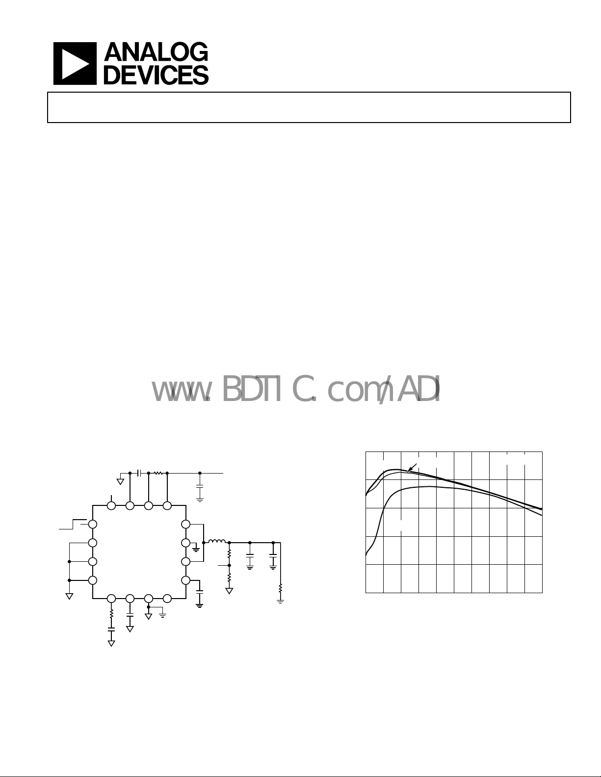
TYPICAL OPERATING CIRCUIT
FB
16 15 14 13
FB PWIN1
ON
OFF
1
2
3
4
120pF
Figure 1. Circuit Configuration of ADP2107 with V
GND
EN
GND
ADP2107-ADJ
GND
GND
SS
COMP
5 6 7 8
70k
0.1
1nF
IN
AGND
IN
VININPUT VOLTAGE = 2.7V TO 5.5V
10
10F
OUTPUT VO LTAGE = 2.5V
12
LX2
2H
11
PGND
85k
10
LX1
PWIN2
NC
FB
V
IN
40k
9
10F
NC = NO CONNECT
10F
OUT
= 2.5 V
4.7F
LOAD
0A TO 2A
Step-Down DC-to-DC Converters
ADP2105/ADP2106/ADP2107
GENERAL DESCRIPTION
The ADP2105/ADP2106/ADP2107 are low quiescent current,
synchronous, step-down dc-to-dc converters in a compact 4 mm ×
4 mm LFCSP_VQ package. At medium to high load currents,
these devices use a current mode, constant frequency pulsewidth modulation (PWM) control scheme for excellent stability
and transient response. To ensure the longest battery life in portable
applications, the ADP2105/ADP2106/ADP2107 use a pulse
frequency modulation (PFM) control scheme under light load
conditions that reduces switching frequency to save power.
The ADP2105/ADP2106/ADP2107 run from input voltages of
2.7 V to 5.5 V, allowing single Li+/Li− polymer cell, multiple
alkaline/NiMH cells, PCMCIA, and other standard power sources.
The output voltage of ADP2105/ADP2106/ADP2107 is adjustable
from 0.8 V to the input voltage (indicated by ADJ), whereas the
ADP2105/ADP2106/ADP2107 are available in preset output
voltage options of 3.3 V, 1.8 V, 1.5 V, and 1.2 V (indicated by x.x V).
Each of these variations is available in three maximum current
levels: 1 A (ADP2105), 1.5 A (ADP2106), and 2 A (ADP2107). The
power switch and synchronous rectifier are integrated for minimal
external part count and high efficiency. During logic controlled
shutdown, the input is disconnected from the output, and it
draws less than 0.1 µA from the input source. Other key features
include undervoltage lockout to prevent deep battery discharge
and programmable soft start to limit inrush current at startup.
100
VIN = 3.3V
95
90
VIN = 5V
85
EFFICIENCY (%)
80
75
02
200 400 600 800 1000 1200 1400 1600 1800
VIN = 3.6V
LOAD CURRENT (mA)
Figure 2. Efficiency vs. Load Current for the ADP2107 with V
06079-002
V
OUT
= 2.5V
06079-001
000
= 2.5 V
OUT
Rev. C
Information furnished by Analog Devices is believed to be accurate and reliable. However, no
responsibility is assumed by Analog Devices for its use, nor for any infringements of patents or other
rights of third parties that may result from its use. Specifications subject to change without notice. No
license is granted by implication or otherwise under any patent or patent rights of Analog Devices.
Trademarks and registered trademarks are the property of their respective owners.
One Technology Way, P.O. Box 9106, Norwood, MA 02062-9106, U.S.A.
Tel: 781.329.4700 www.analog.com
Fax: 781.461.3113 ©2006–2008 Analog Devices, Inc. All rights reserved.
Page 2

ADP2105/ADP2106/ADP2107
www.BDTIC.com/ADI
TABLE OF CONTENTS
Features .............................................................................................. 1
Applications ....................................................................................... 1
General Description ......................................................................... 1
Typical Operating Circuit ................................................................ 1
Revision History ............................................................................... 2
Functional Block Diagram .............................................................. 3
Specifications ..................................................................................... 4
Absolute Maximum Ratings ............................................................ 6
Thermal Resistance ...................................................................... 6
Boundary Condition .................................................................... 6
ESD Caution .................................................................................. 6
Pin Configuration and Function Descriptions ............................. 7
Typical Performance Characteristics ............................................. 8
Theory of Operation ...................................................................... 14
Control Scheme .......................................................................... 14
PWM Mode Operation .............................................................. 14
PFM Mode Operation ................................................................ 14
Pulse-Skipping Threshold ......................................................... 14
100% Duty Cycle Operation (LDO Mode) ............................. 14
Slope Compensation .................................................................. 15
Design Features ........................................................................... 15
Applications Information .............................................................. 16
REVISION HISTORY
9/08—Rev. B to Rev. C
Changes to Table Summary Statement .......................................... 4
Changes to LX Minimum On-Time Parameter, Table 1 ............. 5
7/08—Rev. A to Rev. B
Changes to General Description Section ...................................... 1
Changes to Figure 3 .......................................................................... 3
Changes to Table 1 ............................................................................ 4
Changes to Table 2 ............................................................................ 6
Changes to Figure 4 .......................................................................... 7
Changes to Table 4 ............................................................................ 7
Changes to Figure 26 ...................................................................... 11
Changes to Figure 31 Through Figure 34 .................................... 12
Changes to Figure 35 ...................................................................... 13
Changes to PMW Mode Operation Section and Pulse Skipping
Threshold Section ........................................................................... 14
Changes to Slope Compensation Section .................................... 15
Changes to Setting the Output Voltage Section ........................ 16
Changes to Figure 37 ...................................................................... 16
External Component Selection ................................................ 16
Setting the Output Voltage ........................................................ 16
Inductor Selection ...................................................................... 17
Output Capacitor Selection ....................................................... 18
Input Capacitor Selection .......................................................... 18
Input Filter ................................................................................... 19
Soft Start Period .......................................................................... 19
Loop Compensation .................................................................. 19
Bode Plots .................................................................................... 20
Load Transient Response .......................................................... 21
Efficiency Considerations ......................................................... 22
Thermal Considerations ............................................................ 22
Design Example .............................................................................. 24
External Component Recommendations .................................... 25
Circuit Board Layout Recommendations ................................... 27
Evaluation Board ............................................................................ 28
Evaluation Board Schematic for ADP2107 (1.8 V) ............... 28
Recommended PCB Board Layout (Evaluation Board Layout)
....................................................................................................... 28
Application Circuits ....................................................................... 30
Outline Dimensions ....................................................................... 33
Ordering Guide .......................................................................... 33
Changes to Inductor Selection Section ........................................ 17
Changes to Input Capacitor Selection Section ........................... 18
Changes to Figure 47 through Figure 52 ..................................... 21
Changes to Transition Losses Section and Thermal
Considerations Section .................................................................. 22
Changes to Table 11 ....................................................................... 25
Changes to Circuit Board Layout Recommendations Section..27
Changes to Table 12 ....................................................................... 26
Changes to Figure 53 ...................................................................... 28
Changes to Figure 56 Through Figure 57.................................... 30
Changes to Figure 58 Through Figure 59.................................... 31
Changes to Outline Dimensions .................................................. 33
3/07—Rev. 0 to Rev. A
Updated Format .................................................................. Universal
Changes to Output Characteristics and
LX (Switch Node) Characteristics Sections ................................... 3
Changes to Typical Performance Characteristics Section ........... 7
Changes to Load Transient Response Section ............................ 21
7/06—Revision 0: Initial Version
Rev. C | Page 2 of 36
Page 3
ADP2105/ADP2106/ADP2107
www.BDTIC.com/ADI
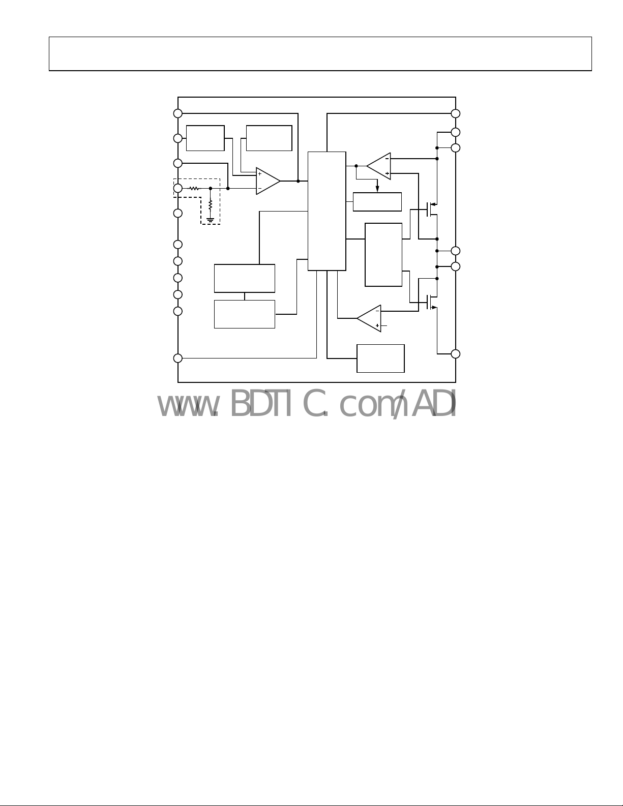
FUNCTIONAL BLOCK DIAGRAM
COMP
SS
FB
FB
AGND
GND
GND
GND
NC
GND
EN
5
SOFT
6
START
16
16
7
FOR PRESET
VOLTAGE
OPTIONS ONLY
2
3
4
8
15
1
REFERENCE
SLOPE
COMPENSATION
OSCILLATOR
0.8V
GM ERROR
AMP
PWM/
PFM
CONTROL
CURRENT SENSE
AMPLI FIER
CURRENT
LIMIT
DRIVER
AND
ANTI-
SHOOT
THROUGH
ZERO CROSS
COMPARATOR
THERMAL
SHUTDOWN
14
9
13
10
12
11
IN
PWIN2
PWIN1
LX1
LX2
PGND
06079-037
Figure 3.
Rev. C | Page 3 of 36
Page 4

ADP2105/ADP2106/ADP2107
www.BDTIC.com/ADI
SPECIFICATIONS
VIN = 3.6 V @ TA = 25°C, unless otherwise noted.1
Table 1.
Parameter Min Typ Max Unit Conditions
INPUT CHARACTERISTICS
Input Voltage Range 2.7 5.5 V −40°C ≤ TJ ≤ +125°C
Undervoltage Lockout Threshold 2.4 V VIN rising
2.2 2.6 V VIN rising, −40°C ≤ TJ ≤ +125°C
2.2 V VIN falling
2.0 2.5 V VIN falling, −40°C ≤ TJ ≤ +125°C
Undervoltage Lockout Hysteresis
OUTPUT CHARACTERISTICS
Output Regulation Voltage 3.267 3.3 3.333 V 3.3 V, load = 10 mA
3.3 V 3.3 V, VIN = 3.6 V to 5.5 V, no load to full load
3.201 3.399 V
1.782 1.8 1.818 V 1.8 V, load = 10 mA
1.8 V 1.8 V, VIN = 2.7 V to 5.5 V, no load to full load
1.746 1.854 V
1.485 1.5 1.515 V 1.5, load = 10 mA
1.5 V ADP210x-1.5 V, VIN = 2.7 V to 5.5 V, no load to full load
1.455 1.545 V
1.188 1.2 1.212 V 1.2 V, load = 10 mA
1.2 V 1.2 V, VIN = 2.7 V to 5.5 V, no load to full load
1.164 1.236 V
Load Regulation 0.4 %/A ADP2105
0.5 %/A ADP2106
0.6 %/A ADP2107
Line Regulation
3
0.1 0.33 %/V ADP2105, measured in servo loop
0.1 0.3 %/V ADP2106 and ADP2107, measured in servo loop
Output Voltage Range 0.8 VIN V ADJ
FEEDBACK CHARACTERISTICS
FB Regulation Voltage 0.8 V ADJ
0.784 0.816 V ADJ, −40°C ≤ TJ ≤ +125°C
FB Bias Current −0.1 +0.1 µA ADJ, −40°C ≤ TJ ≤ +125°C
20 µA 3.3 V output voltage, −40°C ≤ TJ ≤ +125°C
2
200 mV V
3 µA 1.2 V output voltage
6 µA 1.2 V output voltage, −40°C ≤ TJ ≤ +125°C
4 µA 1.5 V output voltage
8 µA 1.5 V output voltage, −40°C ≤ TJ ≤ +125°C
5 µA 1.8 V output voltage
10 µA 1.8 V output voltage, −40°C ≤ TJ ≤ +125°C
10 µA 3.3 V output voltage
falling
IN
3.3 V, V
−40°C ≤ T
1.8 V, V
−40°C ≤ T
= 3.6 V to 5.5 V, no load to full load,
IN
≤ +125°C
J
= 2.7 V to 5.5 V, no load to full load,
IN
≤ +125°C
J
ADP210x-1.5 V, V
−40°C ≤ T
1.2 V, V
−40°C ≤ T
≤ +125°C
J
= 2.7 V to 5.5 V, no load to full load,
IN
≤ +125°C
J
= 2.7 V to 5.5 V, no load to full load,
IN
Rev. C | Page 4 of 36
Page 5
ADP2105/ADP2106/ADP2107
www.BDTIC.com/ADI
Parameter Min Typ Max Unit Conditions
INPUT CURRENT CHARACTERISTICS
IN Operating Current 20 µA ADP210x(ADJ), VFB = 0.9 V
30 µA ADP210x(ADJ), VFB = 0.9 V, −40°C ≤ TJ ≤ +125°C
20 µA
30 µA
IN Shutdown Current
4
0.1 1 µA V
LX (SWITCH) NODE CHARACTERISTICS
LX On Resistance
4
190 mΩ P-channel switch, ADP2105
270 mΩ P-channel switch, ADP2105, −40°C ≤ TJ ≤ +125°C
100 mΩ P-channel switch, ADP2106 and ADP2107
165 mΩ
160 mΩ N-channel synchronous rectifier, ADP2105
230 mΩ
90 mΩ N-channel synchronous rectifier, ADP2106 and ADP2107
140 mΩ
LX Leakage Current
LX Peak Current Limit
4, 5
0.1 1 µA V
5
2.9 A P-channel switch, ADP2107
2.6 3.3 A P-channel switch, ADP2107, −40°C ≤ TJ ≤ +125°C
2.25 A P-channel switch, ADP2106
2.0 2.6 A P-channel switch, ADP2106, −40°C ≤ TJ ≤ +125°C
1.5 A P-channel switch, ADP2105
1.3 1.8 A P-channel switch, ADP2105, −40°C ≤ TJ ≤ +125°C
LX Minimum On-Time 110 ns In PWM mode of operation, −40°C ≤ TJ ≤ +125°C
ENABLE CHARACTERISTICS
EN Input High Voltage 2 V VIN = 2.7 V to 5.5 V, −40°C ≤ TJ ≤ +125°C
EN Input Low Voltage 0.4 V VIN = 2.7 V to 5.5 V, −40°C ≤ TJ ≤ +125°C
EN Input Leakage Current −0.1 µA VIN = 5.5 V, VEN = 0 V, 5.5 V
−1 +1 µA VIN = 5.5 V, VEN = 0 V, 5.5 V, −40°C ≤ TJ ≤ +125°C
OSCILLATOR FREQUENCY 1.2 MHz VIN = 2.7 V to 5.5 V
1 1.4 MHz VIN = 2.7 V to 5.5 V, −40°C ≤ TJ ≤ +125°C
SOFT START PERIOD 750 1000 1200 µs CSS = 1 nF
THERMAL CHARACTERISTICS
Thermal Shutdown Threshold 140
Thermal Shutdown Hysteresis 40
COMPENSATOR
TRANSCONDUCTANCE (g
)
m
CURRENT SENSE AMPLIFIER GAIN (GCS)
50 µA/V
2
1.875 A/V ADP2105
°C
°C
2.8125 A/V ADP2106
3.625 A/V ADP2107
1
All limits at temperature extremes are guaranteed via correlation using standard statistical quality control (SQC). Typical values are at TA = 25°C.
2
Guaranteed by design.
3
The ADP2105/ADP2106/ADP2107 line regulation was measured in a servo loop on the automated test equipment that adjusts the feedback voltage to achieve a
specific COMP voltage.
4
All LX (switch) node characteristics are guaranteed only when the LX1 pin and LX2 pin are tied together.
5
These specifications are guaranteed from −40°C to +85°C.
ADP210x(x.x V) output voltage 10% above regulation
voltage
ADP210x(x.x V) output voltage 10% above regulation
voltage, −40°C ≤ TJ ≤ +125°C
= 0 V
EN
P-channel switch, ADP2106 and ADP2107,
−40°C ≤ TJ ≤ +125°C
N-channel synchronous rectifier, ADP2105,
−40°C ≤ T
≤ +125°C
J
N-channel synchronous rectifier, ADP2106 and ADP2107,
−40°C ≤ T
IN
≤ +125°C
J
= 5.5 V, VLX = 0 V, 5.5 V
Rev. C | Page 5 of 36
Page 6
ADP2105/ADP2106/ADP2107
www.BDTIC.com/ADI
ABSOLUTE MAXIMUM RATINGS
Table 2.
Parameter Rating
IN, EN, SS, COMP, FB to AGND −0.3 V to +6 V
LX1, LX2 to PGND −0.3 V to (VIN + 0.3 V)
PWIN1, PWIN2 to PGND −0.3 V to +6 V
PGND to AGND −0.3 V to +0.3 V
GND to AGND −0.3 V to +0.3 V
PWIN1, PWIN2 to IN −0.3 V to +0.3 V
Operating Junction Temperature Range −40°C to +125°C
Storage Temperature Range −65°C to +150°C
Soldering Conditions JEDEC J-STD-020
Stresses above those listed under Absolute Maximum Ratings
may cause permanent damage to the device. This is a stress
rating only; functional operation of the device at these or any
other conditions above those indicated in the operational
section of this specification is not implied. Exposure to absolute
maximum rating conditions for extended periods may affect
device reliability.
THERMAL RESISTANCE
θJA is specified for the worst-case conditions, that is, a device
soldered in a circuit board for surface-mount packages.
Table 3. Thermal Resistance
Package Type θ
16-Lead LFCSP_VQ/QFN 40 °C/W
Maximum Power Dissipation 1 W
BOUNDARY CONDITION
Natural convection, 4-layer board, exposed pad soldered to the PCB.
ESD CAUTION
JA
Unit
Rev. C | Page 6 of 36
Page 7

ADP2105/ADP2106/ADP2107
www.BDTIC.com/ADI
PIN CONFIGURATION AND FUNCTION DESCRIPTIONS
15 GND
16 FB
14 IN
13 PWIN1
PIN 1
EN 1
GND 2
GND 3
GND 4
INDICATO R
ADP2105/
ADP2106/
ADP2107
TOP VIEW
(Not to Scale)
6
SS
AGND 7
COMP 5
NC = NO CONNECT
Figure 4. Pin Configuration
Table 4. Pin Function Descriptions
Pin No. Mnemonic Description
1 EN
Enable Input. Drive EN high to turn on the device. Drive EN low to turn off the device and reduce the input
current to 0.1 µA.
2, 3, 4, 15 GND
Test Pins. These pins are used for internal testing and are not ground return pins. These pins are to be tied to the
AGND plane as close as possible to the ADP2105/ADP2106/ADP2107.
5 COMP
Feedback Loop Compensation Node. COMP is the output of the internal transconductance error amplifier. Place
a series RC network from COMP to AGND to compensate the converter. See the Loop Compensation section.
6 SS
Soft Start Input. Place a capacitor from SS to AGND to set the soft start period. A 1 nF capacitor sets a 1 ms soft
start period.
7 AGND
Analog Ground. Connect the ground of the compensation components, the soft start capacitor, and the voltage
divider on the FB pin to the AGND pin as close as possible to the ADP2105/ ADP2106/ADP2107. The AGND is
also to be connected to the exposed pad of ADP2105/ADP2106/ADP2107.
8 NC No Connect. This is not internally connected and can be connected to other pins or left unconnected.
9, 13
PWIN2,
PWIN1
Power Source Inputs. The source of the PFET high-side switch. Bypass each PWIN pin to the nearest PGND plane with a
4.7 µF or greater capacitor as close as possible to the ADP2105/ADP2106/ ADP2107. See the Input Capacitor
Selection section.
10, 12 LX1, LX2
Switch Outputs. The drain of the P-channel power switch and N-channel synchronous rectifier. These pins are to
be tied together and connected to the output LC filter between LX and the output voltage.
11 PGND
Power Ground. Connect the ground return of all input and output capacitors to the PGND pin using a power
ground plane as close as possible to the ADP2105/ADP2106/ADP2107. The PGND is then to be connected to the
exposed pad of the ADP2105/ADP2106/ADP2107.
14 IN
Power Input. The power source for the ADP2105/ADP2106/ADP2107 internal circuitry. Connect IN and PWIN1
with a 10 Ω resistor as close as possible to the ADP2105/ADP2106/ADP2107. Bypass IN to AGND with a 0.1 µF or
greater capacitor. See the Input Filter section.
16 FB
Output Voltage Sense or Feedback Input. For fixed output versions, connect to the output voltage. For
adjustable versions, FB is the input to the error amplifier. Drive FB through a resistive voltage divider to set the
output voltage. The FB regulation voltage is 0.8 V.
12 LX2
11 PGND
10 LX1
9 PWIN2
NC 8
06079-003
Rev. C | Page 7 of 36
Page 8
ADP2105/ADP2106/ADP2107
www.BDTIC.com/ADI
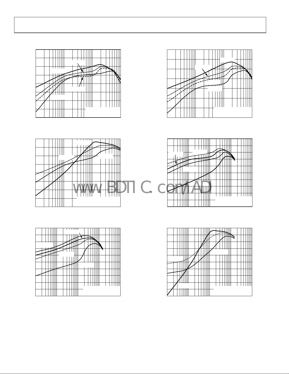
TYPICAL PERFORMANCE CHARACTERISTICS
100
100
95
90
85
80
75
EFFICIENCY (%)
70
65
60
11
VIN = 2.7V
VIN = 5.5V
VIN = 3.6V
VIN = 4.2V
INDUCTOR: SD14, 2.5µH
DCR: 60m
T
= 25°C
A
10 100
LOAD CURRENT (mA)
06079-084
000
Figure 5. Efficiency—ADP2105 (1.2 V Output)
100
95
90
85
80
75
EFFICIENCY (%)
70
65
60
1 1000
VIN = 4.2V
10 100
LOAD CURRENT (mA)
VIN = 3.6V
VIN = 5.5V
INDUCTOR: CDRH5D18, 4.1H
DCR: 43m
T
= 25°C
A
06079-085
Figure 6. Efficiency—ADP2105 (3.3 V Output)
100
95
90
VIN = 2.7V
85
80
75
70
EFFICIENCY (%)
65
60
55
50
1 10k
VIN = 3.6V
VIN = 4.2V
VIN = 5.5V
INDUCTOR: D62L CB, 2µH
DCR: 28m
T
= 25°C
A
10 100 1k
LOAD CURRENT (mA)
06079-062
Figure 7. Efficiency—ADP2106 (1.8 V Output)
95
90
85
80
EFFICIE NCY (%)
75
70
65
1 1000
Figure 8. Efficiency—ADP2105 (1.8 V Output)
100
95
90
VIN = 3.6V
85
80
75
70
EFFICIENCY (%)
65
60
55
50
1 10k
Figure 9. Efficiency—ADP2106 (1.2 V Output)
100
95
90
85
80
VIN = 4.2V
75
70
EFFICIENCY (%)
65
60
55
50
VIN = 3.6V
1 10k
Figure 10. Efficiency—ADP2106 (3.3 V Output)
VIN = 2.7V
VIN = 3.6V
VIN = 4.2V
VIN = 5.5V
INDUCTOR: SD3814, 3.3µH
DCR: 93m
T
= 25°C
A
10 100
LOAD CURRENT (mA)
VIN = 2.7V
VIN = 4.2V
VIN = 5.5V
INDUCTOR: D62L CB, 2µH
DCR: 28m
T
= 25°C
A
10 100 1k
LOAD CURRENT (mA)
VIN = 5.5V
INDUCTOR: D62L CB, 3.3µH
DCR: 47m
T
= 25°C
A
10 100 1k
LOAD CURRENT (mA)
06079-086
06079-008
06079-053
Rev. C | Page 8 of 36
Page 9
ADP2105/ADP2106/ADP2107
www.BDTIC.com/ADI
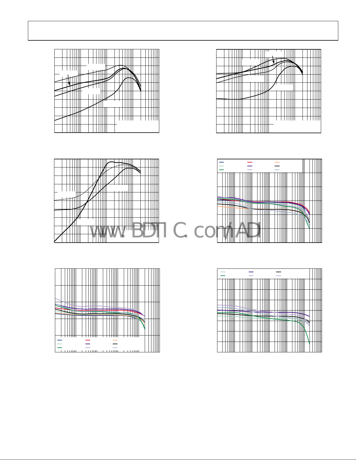
100
95
90
VIN = 3.6V
85
80
75
70
EFFICIENCY (%)
65
60
55
50
1 10k
VIN = 2.7V
VIN = 4.2V
VIN = 5.5V
INDUCTOR: SD12, 1.2µH
DCR: 37m
T
= 25°C
A
10 100 1k
LOAD CURRENT (mA)
Figure 11. Efficiency—ADP2107 (1.2 V)
100
95
90
85
80
VIN = 4.2V
75
70
EFFICIENCY (%)
65
60
55
50
1 10k
VIN = 3.6V
10 100 1k
LOAD CURRENT (mA)
VIN = 5.5V
INDUCTOR: CDRH5D28, 2. 5µH
DCR: 13m
T
= 25°C
A
Figure 12. Efficiency—ADP2107 (3.3 V)
1.85
1.83
06079-010
06079-054
100
95
90
85
80
75
70
EFFICIENCY (%)
65
60
55
50
1 10k
VIN = 2.7V
VIN = 4.2V
10 100 1k
VIN = 3.6V
VIN = 5.5V
INDUCTOR: D62L CB, 1.5µH
DCR: 21m
T
= 25°C
A
LOAD CURRENT (mA)
Figure 14. Efficiency—ADP2107 (1.8 V)
1.23
2.7V, –40° C 2.7V, +25°C 2. 7V, +125°C
3.6V, –40° C 3.6V, +25°C 3. 6V, +125°C
5.5V, –40° C 5.5V, +25°C
1.22
1.21
1.20
1.19
OUTPUT VOLTAGE (V)
1.18
1.17
0.01 10k
0.1 1 10 100 1k
LOAD CURRENT (mA)
5.5V, +125° C
Figure 15. Output Voltage Accuracy—ADP2107 (1.2 V)
3.38
3.6V, –40°C 3.6V, +25°C 3.6V, +125° C
5.5V, –40°C 5.5V, +25°C
3.36
3.34
5.5V, +125° C
06079-063
06079-082
1.81
1.79
OUTPUT VOLTAGE (V)
1.77
2.7V, –40°C 2.7V, +25°C 2.7V, +125° C
3.6V, –40°C 3.6V, +25°C 3.6V, +125° C
5.5V, –40°C 5.5V, +25°C
1.75
0.1 10k
1 10 100 1k
LOAD CURRENT (mA)
5.5V, +125° C
06079-064
Figure 13. Output Voltage Accuracy—ADP2107 (1.8 V)
Rev. C | Page 9 of 36
3.32
3.30
3.28
OUTPUT VOLTAGE (V)
3.26
3.24
3.22
0.01 10k
0.1 1 10 100 1k
LOAD CURRENT (mA)
Figure 16. Output Voltage Accuracy—ADP2107 (3.3 V)
06079-081
Page 10
ADP2105/ADP2106/ADP2107
www.BDTIC.com/ADI
10k
1k
+25°C
–40°C
+125°C
1.2 1.6 2. 0 2.4 2. 8 3.2 3.6 4.0 4.4 4.8 5.2
INPUT VOLTAG E (V)
Figure 17. Quiescent Current vs. Input Voltage
QUIESCENT CURRENT (µA)
100
0.802
0.801
10
1
0.8
190
180
170
160
150
140
130
NMOS SYNCHRONOUS RECTIFI ER
120
SWITCH ON RESISTANCE (m)
110
06079-016
100
2.7 3.0 3.3 3.6 3.9 4.2 4.5 5.1 5.44.8
PMOS POWER SWITCH
INPUT VOLTAGE (V)
06079-093
Figure 20. Switch On Resistance vs. Input Voltage—ADP2105
120
100
PMOS POWER SWITCH
0.800
0.799
0.798
0.797
FEEDBACK VOLT AGE (V)
0.796
0.795
–40 125
–20 0 20 40 60 80 100 120
TEMPERATURE ( °C)
Figure 18. Feedback Voltage vs. Temperature
1.75
1.70
1.65
1.60
1.55
1.50
1.45
1.40
PEAK CURRENT LIMIT (A)
1.35
1.30
1.25
2.7 5.7
3.0 3.3 3.6 3.9 4.2 4.5 4.8 5.1 5.4
INPUT VOLTAGE (V)
ADP2105 (1A)
Figure 19. Peak Current Limit of ADP2105
TA = 25°C
80
60
40
SWITCH ON RESISTANCE (m)
20
06079-017
0
2.7 5.4
NMOS SYNCHRONOUS RECTIFIER
TA = 25°C
3.0 3.3 3.6 3.9 4.2 4.5 4. 8 5.1
INPUT VOLTAGE (V)
06079-018
Figure 21. Switch On Resistance vs. Input Voltage—ADP2106 and ADP2107
1260
1250
1240
1230
1220
1210
SWITCHING FREQUENCY ( kHz)
1200
06079-073
1190
2.7 5.4
3.0 3.3 3.6 3.9 4.2 4.5 4. 8 5.1
+125°C
–40°C
INPUT VOLTAG E (V)
+25°C
06079-021
Figure 22. Switching Frequency vs. Input Voltage
Rev. C | Page 10 of 36
Page 11
ADP2105/ADP2106/ADP2107
www.BDTIC.com/ADI
2.35
2.30
2.25
2.20
2.15
2.10
2.05
2.00
PEAK CURRENT LIMIT (A)
1.95
1.90
1.85
2.7 5.7
3.0 3.3 3.6 3.9 4.2 4.5 4.8 5.1 5.4
INPUT VOLTAGE (V)
ADP2106 (1.5A)
TA = 25°C
Figure 23. Peak Current Limit of ADP2106
3.00
2.95
2.90
2.85
2.80
2.75
2.70
2.65
PEAK CURRENT LIMIT (A)
2.60
2.55
2.50
2.7 5.7
3.0 3.3 3.6 3.9 4.2 4.5 4.8 5.1 5.4
INPUT VOLTAGE (V)
ADP2107 (2A)
TA = 25°C
Figure 24. Peak Current Limit of ADP2107
150
135
120
105
90
75
60
V
45
30
15
PULSE-SKIP PING THRESHO LD CURRENT (mA)
0
2.7 5.7
V
= 1.2V
OUT
V
= 2.5V
= 1.8V
OUT
3.0 3.3 3.6 3.9 4.2 4.5 4.8 5.1 5.4
INPUT VOLTAGE (V)
OUT
TA = 25°C
Figure 25. Pulse-Skipping Threshold vs. Input Voltage for ADP2106
3
1
4
06079-072
135
120
105
90
75
60
45
30
15
06079-071
PULSE-SKIP PING THRESHO LD CURRENT (mA)
Figure 27. Pulse-Skipping Threshold vs. Input Voltage for ADP2105
195
180
165
150
135
120
105
90
75
60
45
30
15
06079-067
PULSE-SKIP PING THRESHO LD CURRENT (mA)
Figure 28. Pulse-Skipping Threshold vs. Input Voltage for ADP2107
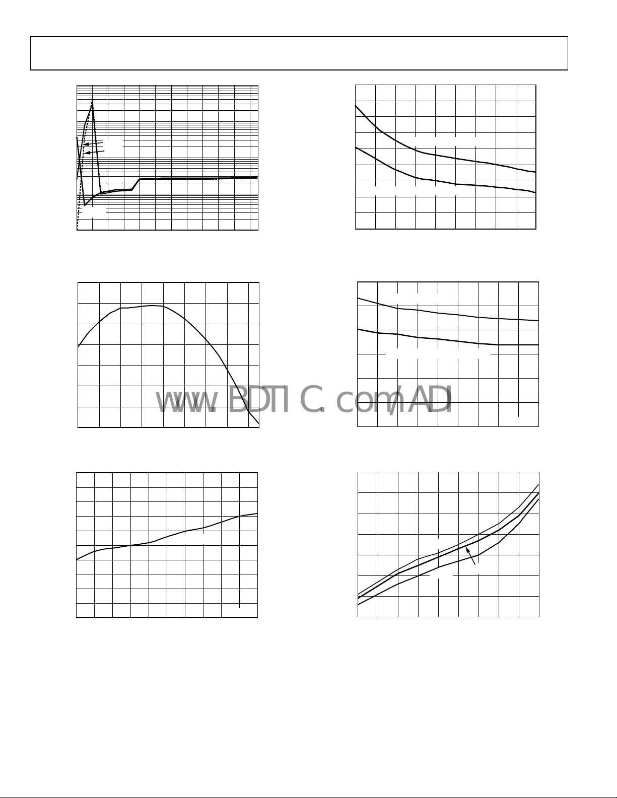
LX (SWITCH) NODE
CH1 1V
INDUCTOR CURRENT
OUTPUT VOLTAGE
M 10µs A CH1 1.78V
45.8%CH4 1ACH3 5V
T
: 260mV
@: 3.26V
Figure 26. Short -Circuit Response at Output
V
= 1.2V
OUT
V
= 1.8V
OUT
0
2.7 5.7
3.0 3.3 3.6 3.9 4.2 4.5 4.8 5.1 5.4
INPUT VOLTAGE (V)
0
2.7 5.7
3.0 3.3 3.6 3.9 4.2 4.5 4.8 5.1 5.4
INPUT VOLTAGE (V)
V
= 2.5V
OUT
TA = 25°C
V
= 1.2V
OUT
V
= 1.8V
OUT
V
= 2.5V
OUT
TA = 25°C
06079-074
06079-066
06079-068
Rev. C | Page 11 of 36
Page 12

ADP2105/ADP2106/ADP2107
www.BDTIC.com/ADI
190
180
170
160
150
140
130
NMOS SYNCHRONOUS RECTIFI ER
120
SWITCH ON RESISTANCE (m)
110
100
2.7 3.0 3.3 3.6 3.9 4.2 4.5 5.1 5.44.8
Figure 29. Switch On Resistance vs. Temperature—ADP2105
140
120
100
80
60
40
SWITCH ON RESISTANCE (m)
20
0
–40
–20 0 20 40 60 80 100 120
Figure 30. Switch On Resistance vs. Temperature—ADP2106 and ADP2107
PMOS POWER SWITCH
INPUT VOLTAGE (V)
PMOS POWER SWITCH
NMOS SYNCHRONOUS RECTIFI ER
JUNCTION TEMPERATURE (°C)
3
LX (SWITCH) NODE
1
4
06079-093
CH1 50mV
OUTPUT VO LTAGE (AC-COUPLED)
INDUCTOR CURRENT
M 400ns A CH3 3.88V
T
17.4%CH4 200mACH3 2V
06079-033
Figure 32. DCM Mode of Operation at Light Load (100 mA)
LX (SWITCH) NODE
3
1
OUTPUT VO LTAGE (AC-COUPLED)
06079-083
4
CH1 20mV
INDUCTOR CURRENT
M 2µs A CH3 1.84V
T
13.4%CH4 1ACH3 2V
06079-034
Figure 33. Minimum Off Time Control at Dropout
LX (SWITCH)
3
1
OUTPUT VO LTAGE (AC-COUPLED)
4
INDUCTOR CURRENT
CH1 50mV
NODE
M 2µs A CH3 3.88V
T
6%CH4 200mACH3 2V
Figure 31. PFM Mode of Operation at Very Light Load (10 mA)
06079-030
Rev. C | Page 12 of 36
LX (SWITCH) NODE
3
1
OUTPUT VO LTAGE (AC-COUPLED)
INDUCTOR CURRENT
4
CH1 20mV
M 1µs A CH3 3.88V
T
17.4%CH4 1ACH3 2V
Figure 34. PWM Mode of Operation at Medium/Heavy Load (1.5 A)
06079-031
Page 13

ADP2105/ADP2106/ADP2107
www.BDTIC.com/ADI
LX (SWITCH) NODE
3
ENABLE VOLTAGE
3
CHANNEL 3
FREQUENCY
= 336.6kHz
INDUCTOR CURRENT
OUTPUT VOLTAGE
1
4
CH1 1V
M 4µs A CH3 1.8V
T
45%CH4 1ACH3 5V
: 2.86A
@: 2.86A
Figure 35. Current Limit Behavior of ADP2107 (Frequency Foldback)
OUTPUT VOLTAGE
1
INDUCTOR CURRENT
4
06079-032
CH1 1V
M 400µs A CH1 1.84V
T
20.2%CH4 500mACH3 5V
06079-035
Figure 36. Startup and Shutdown Waveform (CSS = 1 nF → SS Time = 1 ms)
Rev. C | Page 13 of 36
Page 14

ADP2105/ADP2106/ADP2107
www.BDTIC.com/ADI
THEORY OF OPERATION
The ADP2105/ADP2106/ADP2107 are step-down, dc-to-dc
converters that use a fixed frequency, peak current mode architecture with an integrated high-side switch and low-side synchronous rectifier. The high 1.2 MHz switching frequency and tiny
16-lead, 4 mm × 4 mm LFCSP_VQ package allow for a small stepdown dc-to-dc converter solution. The integrated high-side switch
(P-channel MOSFET) and synchronous rectifier (N-channel
MOSFET) yield high efficiency at medium to heavy loads. Light
load efficiency is improved by smoothly transitioning to variable
frequency PFM mode.
The ADP2105/ADP2106/ADP2107 (ADJ) operate with an input
voltage from 2.7 V to 5.5 V and regulate an output voltage down
to 0.8 V. The ADP2105/ADP2106/ADP2107 are also available with
preset output voltage options of 3.3 V, 1.8 V, 1.5 V, and 1.2 V.
CONTROL SCHEME
The ADP2105/ADP2106/ADP2107 operate with a fixed frequency,
peak current mode PWM control architecture at medium to high
loads for high efficiency, but shift to a variable frequency PFM
control scheme at light loads for lower quiescent current. When
operating in fixed frequency PWM mode, the duty cycle of the
integrated switches is adjusted to regulate the output voltage, but
when operating in PFM mode at light loads, the switching
frequency is adjusted to regulate the output voltage.
The ADP2105/ADP2106/ADP2107 operate in the PWM mode
only when the load current is greater than the pulse-skipping
threshold current. At load currents below this value, the converter
smoothly transitions to the PFM mode of operation.
PWM MODE OPERATION
In PWM mode, the ADP2105/ADP2106/ADP2107 operate at a
fixed frequency of 1.2 MHz set by an internal oscillator. At the
start of each oscillator cycle, the P-channel MOSFET switch is
turned on, putting a positive voltage across the inductor. Current
in the inductor increases until the current sense signal crosses
the peak inductor current level that turns off the P-channel
MOSFET switch and turns on the N-channel MOSFET synchronous rectifier. This puts a negative voltage across the inductor,
causing the inductor current to decrease. The synchronous
rectifier stays on for the remainder of the cycle, unless the
inductor current reaches zero, which causes the zero-crossing
comparator to turn off the N-channel MOSFET. The peak
inductor current is set by the voltage on the COMP pin. The
COMP pin is the output of a transconductance error amplifier that
compares the feedback voltage with an internal 0.8 V reference.
PFM MODE OPERATION
The ADP2105/ADP2106/ADP2107 smoothly transition to the
variable frequency PFM mode of operation when the load current
decreases below the pulse skipping threshold current, switching
only as necessary to maintain the output voltage within regulation.
When the output voltage dips below regulation, the ADP2105/
ADP2106/ADP2107 enter PWM mode for a few oscillator cycles
to increase the output voltage back to regulation. During the wait
time between bursts, both power switches are off, and the output
capacitor supplies all the load current. Because the output voltage
dips and recovers occasionally, the output voltage ripple in this
mode is larger than the ripple in the PWM mode of operation.
PULSE-SKIPPING THRESHOLD
The output current at which the ADP2105/ADP2106/ADP2107
transition from variable frequency PFM control to fixed frequency
PWM control is called the pulse-skipping threshold. The pulseskipping threshold is optimized for excellent efficiency over all
load currents. The variation of pulse-skipping threshold with
input voltage and output voltage is shown in Figure 25, Figure 27,
and Figure 28.
100% DUTY CYCLE OPERATION (LDO MODE)
As the input voltage drops, approaching the output voltage, the
ADP2105/ADP2106/ADP2107 smoothly transition to 100%
duty cycle, maintaining the P-channel MOSFET switch-on continuously. This allows the ADP2105/ADP2106/ADP2107 to regulate
the output voltage until the drop in input voltage forces the Pchannel MOSFET switch to enter dropout, as shown in the
following equation:
V
= I
IN(MIN)
The ADP2105/ADP2106/ADP2107 achieve 100% duty cycle
operation by stretching the P-channel MOSFET switch-on time
if the inductor current does not reach the peak inductor current
level by the end of the clock cycle. When this happens, the oscillator remains off until the inductor current reaches the peak
inductor current level, at which time the switch is turned off and
the synchronous rectifier is turned on for a fixed off time. At
the end of the fixed off time, another cycle is initiated. As the
ADP2105/ADP2106/ADP2107 approach dropout, the switching
frequency decreases gradually to smoothly transition to 100%
duty cycle operation.
OUT
× (R
DS(ON) − P
+ DCR
IND
) + V
OUT(NOM)
Rev. C | Page 14 of 36
Page 15

ADP2105/ADP2106/ADP2107
www.BDTIC.com/ADI
SLOPE COMPENSATION
Slope compensation stabilizes the internal current control loop
of the ADP2105/ADP2106/ADP2107 when operating beyond
50% duty cycle to prevent subharmonic oscillations. It is implemented by summing a fixed, scaled voltage ramp to the current
sense signal during the on-time of the P-channel MOSFET switch.
The slope compensation ramp value determines the minimum
inductor that can be used to prevent subharmonic oscillations
at a given output voltage. For slope compensation ramp values,
see Tabl e 5. For more information see the Inductor Selection
section.
Table 5. Slope Compensation Ramp Values
Part Slope Compensation Ramp Values
ADP2105 0.72 A/µs
ADP2106 1.07 A/µs
ADP2107 1.38 A/µs
DESIGN FEATURES
Enable/Shutdown
Drive EN high to turn on the ADP2105/ADP2106/ADP2107.
Drive EN low to turn off the ADP2105/ADP2106/ADP2107,
reducing the input current below 0.1 μA. To force the
ADP2105/ADP2106/ADP2107 to automatically start when
input power is applied, connect EN to IN. When shut down, the
ADP2105/ADP2106/ADP2107 discharge the soft start capacitor,
causing a new soft start cycle every time they are re-enabled.
Synchronous Rectification
In addition to the P-channel MOSFET switch, the ADP2105/
ADP2106/ADP2107 include an integrated N-channel MOSFET
synchronous rectifier. The synchronous rectifier improves efficiency, especially at low output voltage, and reduces cost and
board space by eliminating the need for an external rectifier.
Current Limit
The ADP2105/ADP2106/ADP2107 have protection circuitry to
limit the direction and amount of current flowing through the
power switch and synchronous rectifier. The positive current
limit on the power switch limits the amount of current that can
flow from the input to the output, and the negative current limit
on the synchronous rectifier prevents the inductor current from
reversing direction and flowing out of the load.
Short-Circuit Protection
The ADP2105/ADP2106/ADP2107 include frequency foldback
to prevent output current runaway on a hard short. When the
voltage at the feedback pin falls below 0.3 V, indicating the possibility of a hard short at the output, the switching frequency is
reduced to 1/4 of the internal oscillator frequency. The reduction
in the switching frequency results in more time for the inductor to
discharge, preventing a runaway of output current.
Undervoltage Lockout (UVLO)
To protect against deep battery discharge, UVLO circuitry is
integrated on the ADP2105/ADP2106/ADP2107. If the
input voltage drops below the 2.2 V UVLO threshold, the
ADP2105/ADP2106/ADP2107 shut down, and both the power
switch and synchronous rectifier turn off. When the voltage
again rises above the UVLO threshold, the soft start period is
initiated, and the part is enabled.
Thermal Protection
In the event that the ADP2105/ADP2106/ADP2107 junction
temperatures rise above 140°C, the thermal shutdown circuit turns
off the converter. Extreme junction temperatures can be the
result of high current operation, poor circuit board design, and/or
high ambient temperature. A 40°C hysteresis is included so that
when thermal shutdown occurs, the ADP2105/ADP2106/
ADP2107 do not return to operation until the on-chip temperature drops below 100°C. When coming out of thermal shutdown,
soft start is initiated.
Soft Start
The ADP2105/ADP2106/ADP2107 include soft start circuitry
to limit the output voltage rise time to reduce inrush current at
startup. To set the soft start period, connect the soft start capacitor
(C
) from SS to AGND. When the ADP2105/ADP2106/ADP2107
SS
are disabled, or if the input voltage is below the undervoltage
lockout threshold, C
ADP2105/ADP2106/ADP2107 are enabled, C
an internal 0.8 µA current source, causing the voltage at SS to rise
linearly. The output voltage rises linearly with the voltage at SS.
is internally discharged. When the
SS
is charged through
SS
Rev. C | Page 15 of 36
Page 16

ADP2105/ADP2106/ADP2107
V
F
F
www.BDTIC.com/ADI
APPLICATIONS INFORMATION
EXTERNAL COMPONENT SELECTION
The external component selection for the ADP2105/ADP2106/
ADP2107 application circuits shown in Figure 37 and Figure 38
depend on input voltage, output voltage, and load current
requirements. Additionally, trade-offs between performance
parameters like efficiency and transient response can be made
by varying the choice of external components.
SETTING THE OUTPUT VOLTAGE
The output voltage of ADP2105/ADP2106/ADP2107(ADJ) is
externally set by a resistive voltage divider from the output
voltage to FB. The ratio of the resistive voltage divider sets the
output voltage, and the absolute value of those resistors sets the
divider string current. For lower divider string currents, the
small 10 nA (0.1 A maximum) FB bias current is to be taken
0.1
V
OUT
16 15 14 13
ON
OFF
FB PWIN1INGND
1
EN
2
GND
3
GND
4
GND
COMP
5 6 7 8
R
COMP
C
COMP
ADP2105/
ADP2106/
ADP2107
SS
AGND
C
SS
Figure 37. Typical Applications Circuit for Fixed Output Voltage Options of ADP2105/ADP2106/ADP2107(x.x V)
0.1
FB
16 15 14 13
GND
ON
OFF
FB PWIN1
1
EN
2
GND
ADP2105/
ADP2106/
ADP2107
GND
GND
COMP
SS
5 6 7 8
COMP
C
3
4
R
COMP
C
SS
Figure 38. Typical Applications Circuit for Adjustable Output Voltage Option of ADP2105/ADP2106/ADP2107(ADJ)
VININPUT VOL TAGE = 2. 7V TO 5.5V
10
LX2
PGND
LX1
PWIN2
NC
NC = NO CONNECT
10
IN
LX2
PGND
LX1
PWIN2
NC
AGND
NC = NO CONNECT
into account when calculating resistor values. The FB bias
current can be ignored for a higher divider string current, but
this degrades efficiency at very light loads.
To limit output voltage accuracy degradation due to FB bias
current to less than 0.05% (0.5% maximum), ensure that the
divider string current is greater than 20 A. To calculate the
desired resistor values, first determine the value of the bottom
divider string resistor (R
V
I
STRING
FB
R =
BOT
where:
V
= 0.8 V, the internal reference.
FB
I
is the resistor divider string current.
STRING
C
IN1
12
11
10
V
IN
9
C
VININPUT VOL TAGE = 2. 7V TO 5.5V
12
11
10
V
IN
9
OUTPUT VOLTAG E = 1.2V, 1.5V, 1. 8V, 3.3
L
C
OUT
IN2
C
IN1
L
R
TOP
FB
C
IN2
R
BOT
) using the following equation:
BOT
V
OUT
LOAD
OUTPUT VOLTAGE
= 0.8V TO V
IN
C
OUT
LOAD
06079-065
06079-038
Rev. C | Page 16 of 36
Page 17

ADP2105/ADP2106/ADP2107
I
www.BDTIC.com/ADI
When R
(R
TOP
The ADP2105/ADP2106/ADP2107(x.x V) include the resistive
voltage divider internally, reducing the external circuitry required.
For improved load regulation, connect the FB to the output
voltage as close as possible to the load.
INDUCTOR SELECTION
The high switching frequency of ADP2105/ADP2106/ADP2107
allows for minimal output voltage ripple even with small inductors.
The sizing of the inductor is a trade-off between efficiency and
transient response. A small inductor leads to larger inductor
current ripple that provides excellent transient response but
degrades efficiency. Due to the high switching frequency of
ADP2105/ADP2106/ADP2107, shielded ferrite core inductors
are recommended for their low core losses and low electromagnetic
interference (EMI).
As a guideline, the inductor peak-to-peak current ripple (I
typically set to 1/3 of the maximum load current for optimal
transient response and efficiency, as shown in the following
equations:
where f
The ADP2105/ADP2106/ADP2107 use slope compensation in
the current control loop to prevent subharmonic oscillations
when operating beyond 50% duty cycle. The fixed slope compensation limits the minimum inductor value as a function of
output voltage.
For the ADP2105
For the ADP2106
For the ADP2107
Inductors 4.7 µH or larger are not recommended because they
may cause instability in discontinuous conduction mode under
light load conditions. It is also important that the inductor be
capable of handling the maximum peak inductor current (I
determined by the following equation:
is determined, calculate the value of the top resistor
BOT
) by using the following equation:
⎡
RR
=
BOTTOP
⎢
⎣
OUT
I ≈
=Δ
L
L
SW
IN
=⇒
IDEAL
is the switching frequency (1.2 MHz).
L > (1.12 µH/V) × V
L > (0.83 µH/V) × V
L > (0.66 µH/V) × V
II
PK
)(LMAXLOAD
⎤
VV
−
FBOUT
⎥
V
FB
⎦
)(
VVV
−×
IN
OUT
LfV
××
SW
VVV
−××
IN
OUT
IV
×
IN
LOAD
OUT
OUT
OUT
Δ
I
⎞
⎛
+=
⎟
⎜
2
⎠
⎝
)(MAX
OUT
)( MAXLOAD
3
)(5.2
H
Ensure that the maximum rms current of the inductor is greater
than the maximum load current and that the saturation current
of the inductor is greater than the peak current limit of the
converter used in the application.
Table 6. Minimum Inductor Value for Common Output
Voltage Options for the ADP2105 (1 A)
V
IN
V
OUT
2.7 V 3.6 V 4.2 V 5.5 V
1.2 V 1.67 µH 2.00 µH 2.14 µH 2.35 µH
1.5 V 1.68 µH 2.19 µH 2.41 µH 2.73 µH
1.8 V 2.02 µH 2.25 µH 2.57 µH 3.03 µH
2.5 V 2.80 µH 2.80 µH 2.80 µH 3.41 µH
3.3 V 3.70 µH 3.70 µH 3.70 µH 3.70 µH
Table 7. Minimum Inductor Value for Common Output
Voltage Options for the ADP2106 (1.5 A)
V
IN
V
OUT
2.7 V 3.6 V 4.2 V 5.5 V
1.2 V 1.11 µH 2.33 µH 2.43 µH 1.56 µH
) is
L
1.5 V 1.25 µH 1.46 µH 1.61 µH 1.82 µH
1.8 V 1.49 µH 1.50 µH 1.71 µH 2.02 µH
2.5 V 2.08 µH 2.08 µH 2.08 µH 2.27 µH
3.3 V 2.74 µH 2.74 µH 2.74 µH 2.74 µH
Table 8. Minimum Inductor Value for Common Output
Voltage Options for the ADP2107 (2 A)
VIN
V
OUT
2.7 V 3.6 V 4.2 V 5.5 V
1.2 V 0.83 µH 1.00 µH 1.07 µH 1.17 µH
1.5 V 0.99 µH 1.09 µH 1.21 µH 1.36 µH
1.8 V 1.19 µH 1.19 µH 1.29 µH 1.51 µH
2.5 V 1.65 µH 1.65 µH 1.65 µH 1.70 µH
3.3 V 2.18 µH 2.18 µH 2.18 µH 2.18 µH
Table 9. Inductor Recommendations for the ADP2105/
ADP2106/ADP2107
Vendo r
Sumida
Toko
Small-Sized Inductors
(< 5 mm × 5 mm)
CDRH2D14, 3D16,
3D28
1069AS-DB3018,
1098AS-DE2812,
Large-Sized Inductors
(> 5 mm × 5 mm)
CDRH4D18, 4D22,
4D28, 5D18, 6D12
D52LC, D518LC,
D62LCB
1070AS-DB3020
Coilcraft
LPS3015, LPS4012,
DO1605T
DO3314
Cooper
)
PK
Bussmann
SD3110, SD3112,
SD3114, SD3118,
SD10, SD12, SD14, SD52
SD3812, SD3814
Rev. C | Page 17 of 36
Page 18

ADP2105/ADP2106/ADP2107
www.BDTIC.com/ADI
OUTPUT CAPACITOR SELECTION
The output capacitor selection affects both the output voltage ripple
and the loop dynamics of the converter. For a given loop crossover
frequency (the frequency at which the loop gain drops to 0 dB), the
maximum voltage transient excursion (overshoot) is inversely
proportional to the value of the output capacitor. Therefore, larger
output capacitors result in improved load transient response. To
minimize the effects of the dc-to-dc converter switching, the crossover frequency of the compensation loop should be less than 1/10
of the switching frequency. Higher crossover frequency leads to
faster settling time for a load transient response, but it can also
cause ringing due to poor phase margin. Lower crossover
frequency helps to provide stable operation but needs large output
capacitors to achieve competitive overshoot specifications.
Therefore, the optimal crossover frequency for the control loop of
ADP2105/ADP2106/ADP2107 is 80 kHz, 1/15 of the switching
frequency. For a crossover frequency of 80 kHz, Figure 39 shows
the maximum output voltage excursion during a 1 A load transient,
as the product of the output voltage and the output capacitor is
varied. Choose the output capacitor based on the desired load
transient response and target output voltage.
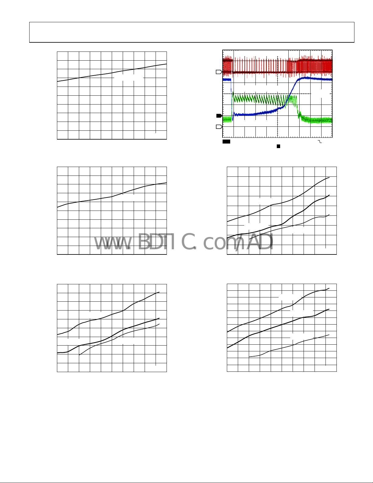
18
17
16
15
14
13
12
11
10
9
8
7
6
5
4
3
2
OVERSHOOT OF OUTPUT VOLTAGE (%)
1
0
15 70
20 25 30 35 40 45 50 55 60 65
OUTPUT CAPACI TOR × OUTPUT VOLT AGE (C)
Figure 39. Percentage Overshoot for a 1 A Load Transient Response vs.
Output Capacitor × Output Voltage
For example, if the desired 1 A load transient response (overshoot)
is 5% for an output voltage of 2.5 V, then from Figure 39
Output Capacitor × Output Voltage = 50 C
C50
≈=⇒ CapacitorOutput
5.2
F20
The ADP2105/ADP2106/ADP2107 have been designed for
operation with small ceramic output capacitors that have low
ESR and ESL. Therefore, they are comfortably able to meet tight
output voltage ripple specifications. X5R or X7R dielectrics are
recommended with a voltage rating of 6.3 V or 10 V. Y5V and Z5U
dielectrics are not recommended, due to their poor temperature
and dc bias characteristics. Table 10 shows a list of recommended
MLCC capacitors from Murata and Taiyo Yuden.
06079-070
When choosing output capacitors, it is also important to
account for the loss of capacitance due to output voltage dc bias.
Figure 40 shows the loss of capacitance due to output voltage dc
bias for three X5R MLCC capacitors from Murata.
20
0
–20
–40
–60
CAPACITANCE CHANGE (%)
–80
1
4.7µF 0805 X5R M URATA GRM21BR61A475K
2
10µF 0805 X5R MURAT A GRM21BR61A106K
3
22µF 0805 X5R MURAT A GRM21BR60J226M
–100
0
Figure 40. Percentage Drop-In Capacitance vs. DC Bias for Ceramic
Capacitors (Information Provided by Murata Corporation)
246
VOLTAGE (VDC)
3
1
2
06079-060
For example, to get 20 µF output capacitance at an output voltage
of 2.5 V, based on Figure 40, as well as to give some margin for
temperature variance, a 22 F and a 10 F capacitor are to be
used in parallel to ensure that the output capacitance is sufficient
under all conditions for stable behavior.
Table 10. Recommended Input and Output Capacitor
Selection for the ADP2105/ADP2106/ADP2107
Vendo r
Capacitor
4.7 µF, 10 V
Murata Taiyo Yuden
GRM21BR61A475K LMK212BJ475KG
X5R 0805
10 F, 10 V
GRM21BR61A106K LMK212BJ106KG
X5R 0805
22 F, 6.3 V
GRM21BR60J226M JMK212BJ226MG
X5R 0805
INPUT CAPACITOR SELECTION
The input capacitor reduces input voltage ripple caused by the
switch currents on the PWIN pins. Place the input capacitors as
close as possible to the PWIN pins. Select an input capacitor
capable of withstanding the rms input current for the maximum
load current in your application.
For the ADP2105, it is recommended that each PWIN pin be
bypassed with a 4.7 F or larger input capacitor. For the ADP2106,
bypass each PWIN pin with a 10 F and a 4.7 F capacitor, and
for the ADP2107, bypass each PWIN pin with a 10 F capacitor.
As with the output capacitor, a low ESR ceramic capacitor is
recommended to minimize input voltage ripple. X5R or X7R
dielectrics are recommended, with a voltage rating of 6.3 V or
10 V. Y5V and Z5U dielectrics are not recommended due to
their poor temperature and dc bias characteristics. Refer to
Tabl e 10 for input capacitor recommendations.
Rev. C | Page 18 of 36
Page 19

ADP2105/ADP2106/ADP2107
www.BDTIC.com/ADI
INPUT FILTER
The IN pin is the power source for the ADP2105/ADP2106/
ADP2107 internal circuitry, including the voltage reference and
current sense amplifier that are sensitive to power supply noise.
To prevent high frequency switching noise on the PWIN pins from
corrupting the internal circuitry of the ADP2105/ADP2106/
ADP2107, a low-pass RC filter should be placed between the IN
pin and the PWIN1 pin. The suggested input filter consists of
a small 0.1 F ceramic capacitor placed between IN and AGND
and a 10 resistor placed between IN and PWIN1. This forms a
150 kHz low-pass filter between PWIN1 and IN that prevents any
high frequency noise on PWIN1 from coupling into the IN pin.
SOFT START PERIOD
To set the soft start period, connect a soft start capacitor (CSS) from
SS to AGND. The soft start period varies linearly with the size
of the soft start capacitor, as shown in the following equation:
= CSS × 109 ms
T
SS
For a soft start period of 1 ms, a 1 nF capacitor must be
connected between SS and AGND.
LOOP COMPENSATION
The ADP2105/ADP2106/ADP2107 utilize a transconductance
error amplifier to compensate the external voltage loop. The
open loop transfer function at angular frequency (s) is given by
⎞
⎛
OUT
⎞
sZ
V
REF
⎟
⎜
⎟
⎜
⎟
⎝
⎠
⎟
V
OUT
⎠
⎛
COMP
⎜
GGsH)()(
=
m
CS
⎜
sC
⎝
where:
V
is the internal reference voltage (0.8 V).
REF
V
is the nominal output voltage.
OUT
(s) is the impedance of the compensation network at the
Z
COMP
angular frequency.
C
is the output capacitor.
OUT
is the transconductance of the error amplifier (50 A/V
g
m
nominal).
is the effective transconductance of the current loop.
G
CS
= 1.875 A/V for the ADP2105.
G
CS
G
= 2.8125 A/V for the ADP2106.
CS
= 3.625 A/V for the ADP2107.
G
CS
The transconductance error amplifier drives the compensation
network that consists of a resistor (R
) and capacitor (C
COMP
COMP
)
connected in series to form a pole and a zero, as shown in the
following equation:
⎛
sC
1
COMP
⎞
1
+
⎜
⎟
=
⎜
⎟
⎠
sC
⎝
COMP
⎛
⎜
+=
RsZ
)(
COMPCOMP
⎜
⎝
⎞
CsR
COMPCOMP
⎟
⎟
⎠
At the crossover frequency, the gain of the open loop transfer
function is unity. For the compensation network impedance at
the crossover frequency, this yields the following equation:
⎛
⎜
=
)(
CROSSCOMP
⎜
⎝
m
FFZ)π2(
CROSS
GG
⎞
⎛
⎟
⎜
⎜
⎟
CS
⎝
⎠
⎞
VC
OUTOUT
⎟
⎟
V
REF
⎠
where:
F
= 80 kHz, the crossover frequency of the loop.
CROSS
C
is determined from the Output Capacitor Selection
OUTVOUT
section.
To ensure that there is sufficient phase margin at the crossover
frequency, place the compensator zero at 1/4 of the crossover
frequency, as shown in the following equation:
F
CROSS
4
⎞
CR
⎟
⎠
COMPCOMP
1
⎛
)π2( =
⎜
⎝
Solving the three equations in this section simultaneously yields
the value for the compensation resistor and compensation
capacitor, as shown in the following equation:
COMP
COMP
⎛
⎜
=
8.0
⎜
⎝
=
2
RFCπ
m
FR)π2(
GG
COMPCROSS
CROSS
CS
⎞
⎛
⎟
⎜
⎜
⎟
⎝
⎠
⎞
VC
OUTOUT
⎟
⎟
V
REF
⎠
Rev. C | Page 19 of 36
Page 20

ADP2105/ADP2106/ADP2107
www.BDTIC.com/ADI
BODE PLOTS
60
50
40
30
20
10
0
LOOP GAIN (dB)
OUTPUT VOLTAGE = 1.8V
–10
INPUT VOLTAGE = 5.5V
LOAD CURRENT = 1A
–20
INDUCTOR = 2. 2µH (LPS4012)
OUTPUT CAPACITOR = 22µ F + 22µF
–30
COMPENSATION RESISTOR = 180k
COMPENSATION CAPACITOR = 56pF
–40
1 300
Figure 41. ADP2106 Bode Plot at VIN = 5.5 V, V
60
50
40
30
20
10
0
LOOP GAIN (dB)
OUTPUT VOLTAGE = 1.8V
–10
INPUT VOLTAGE = 3.6V
LOAD CURRENT = 1A
–20
INDUCTOR = 2. 2µH (LPS4012)
OUTPUT CAPACI TOR = 22µF + 22µF
–30
COMPENSATI ON RESIS TOR = 180k
COMPENSATI ON CAPACITO R = 56pF
–40
1 300
Figure 42. ADP2106 Bode Plot at V
60
50
40
30
20
10
0
LOOP GAIN (dB)
OUTPUT VOLTAGE = 1.2V
–10
INPUT VOLTAGE = 3.6V
LOAD CURRENT = 1A
–20
INDUCTOR = 3. 3µH (SD3814)
OUTPUT CAPACI TOR = 22µF + 22µF + 4. 7µF
–30
COMPENSATION RESIS TOR = 267k
COMPENSATI ON CAPACITO R = 39pF
–40
1 300
Figure 43. ADP2105 Bode Plot at V
LOOP GAIN
PHASE
MARGIN = 48°
LOOP PHASE
CROSSOVER
FREQUENCY = 87kHz
10 100
FREQUENCY (kHz)
NOTES
1. EXTERNAL CO MPONENTS WERE CHOSEN FOR A
5% OVERSHOOT FOR A 1A LOAD TRANSIENT.
= 1.8 V and Load = 1 A
OUT
LOOP GAIN
PHASE
MARGIN = 52°
LOOP PHASE
CROSSOVER
FREQUENCY = 83kHz
10 100
NOTES
1. EXTERNAL CO MPONENTS W ERE CHOSEN FO R A
5% OVERSHOO T FOR A 1A LOAD TRANSIENT .
LOOP GAIN
LOOP PHASE
NOTES
1. EXTERNAL CO MPONENTS WERE CHOSEN FOR A
5% OVERSHOOT FOR A 1A LOAD TRANSIENT.
FREQUENCY (kHz)
= 3.6 V, V
IN
FREQUENCY = 71kHz
10 100
FREQUENCY (kHz)
= 3.6 V, V
IN
OUT
PHASE
MARGIN = 51°
CROSSOVER
OUT
= 1.8 V, and Load = 1 A
= 1.2 V, and Load = 1 A
ADP2106
ADP2106
ADP2105
0
45
90
135
180
0
45
90
135
180
0
45
90
135
180
LOOP P HASE (Degrees)
LOOP PHASE (Degrees)
LOOP PHASE (Degrees)
60
50
40
30
20
10
0
LOOP GAIN (dB)
OUTPUT VOLTAGE = 1.2V
–10
INPUT VOLTAGE = 5.5V
LOAD CURRENT = 1A
–20
INDUCTOR = 3.3µH (SD3814)
OUTPUT CAPACI TOR = 22µF + 22µF + 4. 7µF
–30
COMPENSATI ON RESISTOR = 267k
COMPENSATI ON CAPACITO R = 39pF
–40
1 300
06079-055
LOOP GAIN
LOOP PHASE
CROSSOVER
FREQUENCY = 79kHz
10 100
FREQUENCY (kHz)
NOTES
1. EXTERNAL CO MPONENTS WERE CHOSEN FOR A
5% OVERSHOOT FOR A 1A LOAD TRANSIENT.
Figure 44. ADP2105 Bode Plot at VIN = 5.5 V, V
60
50
40
30
20
10
0
LOOP GAIN (dB)
–10
–20
–30
–40
1 300
06079-056
LOOP GAIN
LOOP PHASE
OUTPUT VO LTAGE = 2.5V
INPUT VOLTAGE = 5V
LOAD CURRENT = 1A
INDUCTOR = 2µH (D62LCB)
OUTPUT CAPACI TOR = 10µF + 4.7µF
COMPENSATION RESISTOR = 70k
COMPENSATI ON CAPACITO R = 120pF
FREQUENCY (kHz)
NOTES
1. EXTERNAL CO MPONENTS WERE CHOSEN FOR A
10% OVERSHOOT FOR A 1A L OAD TRANSIENT.
CROSSOVER
FREQUENCY = 76kHz
10 100
Figure 45. ADP2107 Bode Plot at VIN = 5 V, V
60
50
40
30
20
10
0
LOOP GAIN (dB)
–10
–20
–30
–40
1 300
06079-057
Figure 46. ADP2107 Bode Plot at V
LOOP GAIN
LOOP PHASE
OUTPUT VOLTAGE = 3.3V
INPUT VOLTAGE = 5V
LOAD CURRENT = 1A
INDUCTOR = 2. 5µH (CDRH5D28)
OUTPUT CAP ACITOR = 10µF + 4.7µF
COMPENSATION RESISTOR = 70k
COMPENSATI ON CAPACITO R = 120pF
FREQUENCY (kHz)
NOTES
1. EXTERNAL CO MPONENTS WERE CHOSEN FOR A
10% OVERSHOOT FOR A 1A L OAD TRANSIENT.
CROSSOVER
FREQUENCY = 67kHz
10 100
= 5 V, V
IN
ADP2105
PHASE
MARGIN = 49°
= 1.2 V and Load = 1 A
OUT
ADP2107
PHASE
MARGIN = 65°
= 2.5 V and Load = 1 A
OUT
ADP2107
PHASE
MARGIN = 70°
= 3.3 V, and Load = 1 A
OUT
0
45
90
135
180
LOOP PHASE (Degrees)
06079-058
0
45
90
135
180
LOOP PHASE (Degrees)
06079-059
0
45
90
135
180
LOOP P HASE (Degrees)
06079-069
Rev. C | Page 20 of 36
Page 21

ADP2105/ADP2106/ADP2107
www.BDTIC.com/ADI
LOAD TRANSIENT RESPONSE
T
3
OUTPUT CURRENT
T
3
OUTPUT CURRENT
OUTPUT VO LTAGE (AC-COUPLED)
2
1
CH3 1.00A
OUTPUT CAPACI TOR: 22µ F + 22µF + 4.7µF
INDUCTOR: SD14, 2.5µH
COMPENSATION RESIS TOR: 270k
COMPENSATI ON CAPACITO R: 39pF
LX NODE (SWITCH NODE)
CH2 100mV~CH1 2.00V
M 20.0µs A CH3 700mA
T 10.00%
Figure 47. 1 A Load Transient Response for ADP2105-1.2
with External Components Chosen for 5% Overshoot
T
3
2
OUTPUT CURRENT
OUTPUT VO LTAGE (AC-COUPLED)
OUTPUT VO LTAGE (AC-COUPLED)
2
1
LX NODE (SW ITCH NODE)
CH3 1.00A
OUTPUT CAPACI TOR: 22µF + 4.7µF
INDUCTOR: SD14, 2.5µH
COMPENSATION RESISTOR: 135k
06079-087
COMPENSATI ON CAPACITOR: 82pF
CH2 100mV~CH1 2.00V
M 20.0µs A CH3 700mA
T 10.00%
06079-090
igure 50. 1 A Load Transient Response for ADP2105-1.2F
with External Components Chosen for 10% Overshoot
T
3
OUTPUT VO LTAGE (AC-COUPLED)
2
OUTPUT CURRENT
1
CH3 1.00A
OUTPUT CAPACI TOR: 22µ F + 22µF
INDUCTOR: SD3814, 3.3µH
COMPENSATION RESIS TOR: 270k
COMPENSATI ON CAPACITO R: 39pF
LX NODE (SWITCH NODE)
CH2 100mV~CH1 2.00V
M 20.0µs A CH3 700mA
T 10.00%
Figure 48. 1 A Load Transient Response for ADP2105-1.8
with External Components Chosen for 5% Overshoot
T
3
2
1
CH3 1.00A
OUTPUT CAPACITOR: 22µF + 4.7µF
INDUCTOR: CDRH5D18, 4. 1µH
COMPENSATION RESISTOR: 270k
COMPENSATION CAPACITOR: 39pF
OUTPUT CURRENT
OUTPUT VO LTAGE (AC-COUPLED)
LX NODE (SW ITCH NODE)
CH2 200mV~CH1 2.00V
M 20.0µs A CH3 700mA
T 10.00%
Figure 49. 1 A Load Transient Response for ADP2105-3.3
with External Components Chosen for 5% Overshoot
06079-088
06079-089
Rev. C | Page 21 of 36
1
CH3 1.00A
OUTPUT CAPACI TOR: 10µF + 10µF
INDUCTOR: SD3814, 3.3µH
COMPENSATION RESISTOR: 135k
COMPENSATI ON CAPACITOR: 82pF
LX NODE (SW ITCH NODE)
CH2 100mV~CH1 2.00V
M 20.0µs A CH3 700mA
T 10.00%
Figure 51. 1 A Load Transient Response for ADP2105-1.8
with External Components Chosen for 10% Overshoot
T
3
OUTPUT VO LTAGE (AC-COUPLED)
2
1
CH3 1.00A
OUTPUT CAPACI TOR: 10µF + 4.7µF
INDUCTOR: CDRH5D18, 4.1µH
COMPENSATION RESISTOR: 135k
COMPENSATI ON CAPACITOR: 82pF
OUTPUT CURRENT
LX NOD E (SWI TCH NO DE)
CH2 200mV~CH1 2.00V
M 20.0µs A CH3 700mA
T 10.00%
Figure 52. 1 A Load Transient Response for ADP2105-3.3
with External Components Chosen for 10% Overshoot
06079-091
06079-092
Page 22

ADP2105/ADP2106/ADP2107
V
www.BDTIC.com/ADI
EFFICIENCY CONSIDERATIONS
Efficiency is the ratio of output power to input power. The high
efficiency of the ADP2105/ADP2106/ADP2107 has two distinct
advantages. First, only a small amount of power is lost in the dcto-dc converter package that reduces thermal constraints. Second,
the high efficiency delivers the maximum output power for the
given input power, extending battery life in portable applications.
There are four major sources of power loss in dc-to-dc
converters like the ADP2105/ADP2106/ADP2107:
• Power switch conduction losses
• Inductor losses
• Switching losses
• Tr a n si t ion lo s s es
Power Switch Conduction Losses
Power sw output
current t channel
synchronous rectifier, which have intern
associated with them. The amount of power loss can be approx
mated by
where D = V
The internal resistance of the power switches increases with
temperature but decreases with higher input voltage. Figure 20
and Figure 21 show the change in R
whereas Figure 29 and Figure 30 show the change in
temperature for both power devices.
Inductor Losses
Inductor conduction lo
through the inductor, w
associated with it. Larger sized inducto
which can improve inductor conduction losses.
Inductor core losses are related to the magnetic permeability of
the core material. Because the ADP2105/ADP2106/ADP2107
are high switching frequency dc-to-dc converters, shielded ferrite
core materi
The
Switching Losses
Switching losses are associated with the current drawn by the
driver to turn on and turn off the power devices at the
switching frequency. Each time a power device gate is turned o
and turned off, the driver transfers a
supply to the gate a
The amount of power loss can by calculated by
where:
(C
f
SW
itch conduction losses are caused by the flow of
hrough the P-channel power switch and the N-
al resistances (R
P
SW − COND
= [R
OUT/VIN
DS(ON) − P
.
× D + R
DS(ON) − N
vs. input voltag
DS(ON)
× (1 − D)] × I
R
DS(ON)
OUT
sses are caused by the flow of current
hich has an internal resistance (DCR)
rs have smaller DCR,
al is recommended for its low core losses and low EMI.
total amount of inductor power loss can be calculated by
P
= DCR × I
L
OUT
2
Core Losses
+
charge Q from the input
nd then from the gate to ground.
P
GATE − P
SW
= (C
+ C
GATE − P
GATE − N
+ C
GATE − N
) ≈ 600 pF.
) × V
2
IN
× fSW
= 1.2 MHz, the switching frequency.
DS(ON)
2
e,
vs.
)
i-
Transition Losses
Transition losses occur because the P-channel MOSFET power
switch cannot turn on or turn off instantaneously. At the middle o
an L e t r switch is providing all
X (switch) nod ransition, the powe
the in o drain voltage of the
ductor current, while the source t
power switch is half t
he input voltage, resulting in power loss.
f
Transition losses increase with load current and input voltage
and occur twice for each switching cycle.
The amount of power loss can be calculated by
P ×+××= )(
TRAN
where t
(swi ns.
tch) node, and are both approximately 3
THERM
IN
OUT
2
ON
and t
are the rise time and fall time of the LX
OFF
AL CONSIDERATIONS
In most applications, the ADP2105/ADP2106/AD
dissipate a lot of heat due to their high ef
applications with high
ambient temperature, low supply voltage,
fttI
SWOFFON
P2107 do not
ficiency. However, in
and high duty cycle, the heat dissipated in the package is large
enough that it can cause the junction temperature of the die to
exceed the maximum junction temperature of 125°C. Once the
junction temperature exceeds 140°C, the converter goes into
thermal shutdown. To prevent any permanent damage it recover
s
only after the junction temperature has decreased below 100°C.
Therefore, thermal analysis for the chosen a
is very important to guarantee reliable performa
pplication solution
nce over all
conditions.
The junction temperature of the die is th m of the ambient
tempera ure of t e environment and the temperature rise o
t h f the
package due to the power dissipation, as shown in the follo
e su
wing
equation:
T = T + T
J A R
where:
T
is the junction temperature.
J
T
is the ambient temperature.
A
T
is the rise in temperature of the package due to the power
R
dissipation in the package.
The rise in temperature of the package is directly proportiona
l
to the power dissipation in the package. The proportionality
constant for this relationship is defined as the thermal resistance
from the junction of the die to the ambient temperature, as
shown in the following equation:
T
n
R
where:
T
is the rise in temperature of the package.
R
P
is the power dissipation in the package.
D
θ
is the th
JA
ient temperatur
amb e of the package.
P
= θJA ×
D
ermal resistance from the junction of the die to the
Rev. C | Page 22 of 36
Page 23

ADP2105/ADP2106/ADP2107
www.BDTIC.com/ADI
for the LFCSP_VQ package is 40°C/W, as shown in
For example, in an application where the ADP2107(1.8 V) is
used with an input voltage o
f 3.6 V, a load current of 2 A, and a
maximum ambient temperature of 85°C, at a load current of 2 A,
the most significant contributor of power dissipation in the dc-todc converter package is the conduction loss of the power switches
Using the graph of switch on resistance vs. temperature (see
Figure 30), as well as the equation of power loss given in the
Pow S c duction Losses ser wit h Con
e package can
in th be calculated by the following:
P
SW − COND
= [R
DS(ON) − P
× D + R
[109 m × 0.5 + 90 m × 0.5] × (2 A)
ection, the power dissipation
2
DS(ON) − N
× (1
− D)] × I
2
≈ 400 mW
OUT
=
.
The θ
JA
Tabl e 3. Therefore, the rise in temperature of the package due to
power dissipation is
T
= θJA × PD = 40°C/W × 0.40 W = 16°C
R
The junction temperature of the converter is
= TA + TR = 85°C + 16°C = 101°C
T
J
Because the junction temperature of the converter is below the
maximum junction temperature of 125°C, this application operates
reliably from a thermal point of view.
Rev. C | Page 23 of 36
Page 24

ADP2105/ADP2106/ADP2107
www.BDTIC.com/ADI
DESIGN EXAMPLE
Consider an application with the following specifications:
Input Voltage = 3.6 V to 4.2 V.
Output Voltage = 2 V.
Typical Output Current = 600 mA.
Maximum Output Current = 1.2 A.
Soft Start Time = 2 ms.
Overshoot ≤ 100 mV under all load transient conditio
Choose the dc-to-dc converter that satisfies the maximum
1.
output current requirement. Because the maximum o
current for this application is 1.2 A, the ADP2106 with
maximum output current of 1.5 A is ideal for this
application.
2.
See whether the output voltage desired is available as a
fixed output voltage option. Because 2 V is not one of the
fixed output voltage options available, choose the adjustable
version of ADP2106.
3.
The first step in external component selection for an
adjustable version converter is to calculate the resistance of
the resistive voltage divider that sets the output voltage.
OUT
V8.0
===
A20
−
VV
FB
V
FB
k40
⎤
⎥
⎦
⎡
k40
×=
⎢
⎢
⎣
V
R
BOT
FB
I
STRING
⎡
=
RR
⎢
BOTTOP
⎣
Calculate the minimum inductor value as follows:
For the ADP2106:
L > (0.83 H/V) × V
⇒
L > 0.83 H/V × 2 V
⇒
L > 1.66 H
Ne
xt, calculate the ideal inductor value that sets the
OUT
inductor peak-to-peak current ripple (I
maximum load current at the maximum input voltage as
follows:
−××
)(5.2
VVV
IN
= H
L
IDEAL
OUT
×
IV
IN
LOAD
−××
)22.4(25.2
×
2.12.4
=
OUT
)(MAX
H2.18H
=
ns.
⎤
V8.0V2
−
⎥
V8.0
⎥
⎦
) to 1/3 of the
L
utput
a
=
The closest standard inductor value is 2.2 H. The maximum
4.
rrms cu rent of the inductor is to be greater than 1.2 A, and
the saturation current of the inductor is to be greater than
2 A. One inductor that meets these criter
ia is the LPS4012-
2.2 H from Coilcraft.
5.
Choose the output capacitor based on the transient response
requirements. The worst-case load transient is 1.2 A, for
which the overshoot must be less than 100 mV, which is 5%
of the output voltage. For a 1 A lo
ad transient, the overshoot
must be less than 4% of the output voltage, then from
Figure 39:
Output Capacitor × Output Voltage = 60 C
C60
≈=⇒ CapacitorOutput
V0.2
F30
Taking into account the loss of capacitance due to dc bias, as
shown in Figure 40, two 22 F X5R MLCC capacitors from
Murata (GRM21BR60J226M) are sufficient for this
application.
6.
Because the ADP2106 is being used in this application, the
input capacitors are 10 F and 4.7 F X5R Murata capacitors
(GRM21BR61A106K and GRM21BR61A475K).
7.
The input filter consists of a small 0.1 F ceramic capacitor
k60
placed between IN and AGND and a 10 resistor placed
between IN and PWIN1.
8.
Choose a soft start capacitor of 2 nF to achieve a soft start
time of 2 ms.
9.
Calculate the compensation resistor and capacitor as
follows:
m
==
FR)π2(
CROSS
GG
⎞
⎛
⎟
⎜
⎜
⎟
CS
V/A8125.2V/A50
V
⎝
⎠
⎛
⎞
⎜
⎟
⎜
⎟
⎝
⎠
2
××
⎞
VC
OUTOUT
⎟
=
⎟
REF
⎠
⎞
V2F30
×
⎟
k215
⎟
V8.0
⎠
k215kHz80π
pF39
=
⎛
⎜
=
COMP
⎛
⎜
8.0 =
⎜
⎝
C
COMP
π
8.0
⎜
⎝
kHz80)π2(
×
×
2
RF
COMPCROSS
Rev. C | Page 24 of 36
Page 25

ADP2105/ADP2106/ADP2107
www.BDTIC.com/ADI
EXTERNAL COMPON
For popular output voltage options at 80 kHz crossover fre ncy with 10% overshoot for a 1 A load transient (refer to Figure 37 and
ENT RECOMMENDATIONS
que
Figure 38).
1
F) C
(μ
ponents
1
(μF) C
IN2
OUT
2
(μF)
L (μH) R
(kΩ) C
COMP
(pF) R
MP
CO
TOP
3
(kΩ) R
BOT
3
(kΩ)
Table 11. Recommended External Com
Part V
(V) C
OUT
IN1
ADP2105(ADJ) 0.9 4.7 4.7 22 + 10 2.0 135 82 5 40
ADP2105(ADJ) 1.2 4.7 4.7 22 + 4.7 2.5 135 82 20 40
ADP2105(ADJ) 1.5 4.7 4.7 10 + 10 3.0 135 82 35 40
ADP2105(ADJ) 1.8 4.7 4.7 10 + 10 3.3 135 82 50 40
ADP2105(ADJ) 2.5 4.7 4.7 10 + 4.7 3.6 135 82 85 40
ADP2105(ADJ) 3.3 4.7 4.7 10 + 4.7 82 125 40 4.1 135
ADP2106(ADJ) 0.9 4.7 10 22 + 10 1.5 40 90 100 5
ADP2106(ADJ) 1.2 4.7 10 22 + 4.7 1.8 40 90 100 20
ADP2106(ADJ) 1.5 4.7 10 10 + 10 2.0 90 100 35 40
ADP2106(ADJ) 1.8 4.7 10 10 + 10 2.2 90 100 50 40
ADP2106(ADJ) 2.5 4.7 10 10 + 4.7 2.5 90 100 85 40
ADP2106(ADJ) 3.3 4.7 10 10 + 4.7 3.0 90 100 125 40
ADP2107(ADJ) 0.9 10 10 22 + 10 1.2 70 120 5 40
ADP2107(ADJ) 1.2 10 10 22 + 4.7 1.5 70 120 20 40
ADP2107(ADJ) 1.5 10 10 10 + 10 1.5 70 120 35 40
ADP2107(ADJ) 1.8 10 10 10 + 10 1.8 70 120 50 40
ADP2107(ADJ) 2.5 10 10 10 + 4.7 1.8 70 120 85 40
ADP2107(ADJ) 3.3 10 10 10 + 4.7 2.5 70 120 125 40
ADP2105-1.2 1.2 4.7 4.7 22 + 4.7 2.5 135 82 N/A N/A
ADP2105-1.5 1.5 4.7 4.7 10 + 10 3.0 135 82 N/A N/A
ADP 10 + 10 2105-1.8 1.8 4.7 4.7 3.3 135 82 N/A N/A
ADP2105-3.3 10 + 4.7 3.3 4.7 4.7 4.1 135 82 N/A N/A
ADP 4.7 10 22 + 4.7 2106-1.2 1.2 1.8 90 100 N/A N/A
ADP 4.7 10 10 + 10 2106-1.5 1.5 2.0 90 100 N/A N/A
ADP210 .7 10 10 + 10 100 N/A N/A 6-1.8 1.8 4 2.2 90
ADP210 4.7 10 10 + 4.7 3.0 90 100 N/A N/A 6-3.3 3.3
ADP 1.5 70 120 N/A /A 2107-1.2 1.2 10 10 22 + 4.7 N
ADP 10 1.5 70 120 N/A N/A 2107-1.5 1.5 10 10 10 +
ADP 0 1.8 70 120 N/A N/A 2107-1.8 1.8 10 10 10 + 1
ADP 3.3 10 10 10 + 4.7 2.5 70 120 N/A N/A 2107-3.3
1
4.7 F 0805 X5R 10 V Murata—GRM21BR61A475KA73L. 10 F 0805 X5R 10 V Murata—GRM21BR61A106KE19L.
2
4.7 F 0805 X5R 10 V Murata—GRM21BR61A475KA73L. 10 F 0805 X5R 10 V Murata—GRM21BR61A106KE19L. 22 F 0805 X5R 6.3 V Murata—GRM21BR60J226ME39L.
3
0.5% accuracy resistor.
Rev. C | Page 25 of 36
Page 26

ADP2105/ADP2106/ADP2107
www.BDTIC.com/ADI
For popular output voltage options at 80 kHz crossover frequency with 5
Figure 38).
% overshoot for a 1 A load transient (refer to Figure 37 and
Table 12. Re
Part V
commended External Components
(V) C
OUT
1
(μF) C
IN1
IN2
1
(μ
F) C
2
(μF) L (μH) R
OUT
COMP
(kΩ) C
(pF) R
COMP
3
(kΩ) R
TOP
BOT
3(kΩ)
ADP2105(ADJ) 0.9 4.7 4.7 22 + 22 + 22 2.0 270 39 5 40
ADP2105(ADJ) 7 3 21.2 4.7 4.7 22 + 22 + 4. 2.5 270 9 0 40
ADP2105(ADJ) 1.5 7 3 34. 4.7 22 + 22 3.0 270 9 5 40
ADP2105(ADJ) 1.8 7 3 54. 4.7 22 + 22 3.3 270 9 0 40
ADP2105(ADJ) 2.5 7 3 84. 4.7 22 + 10 3.6 270 9 5 40
ADP2105(ADJ) 3.3 7 3 14. 4.7 22 + 4.7 4.1 270 9 25 40
ADP2106(ADJ) 0.9 7 22 5 5 4. 10 22 + 22 + 1.5 180 6 40
ADP2106(ADJ) 1.2 7 4.7 5 24. 10 22 + 22 + 1.8 180 6 0 40
ADP2106(ADJ) 1.5 7 5 34. 10 22 + 22 2.0 180 6 5 40
ADP2106(ADJ) 1.8 7 5 54. 10 22 + 22 2.2 180 6 0 40
ADP2106(ADJ) 2.5 7 5 84. 10 22 + 10 2.5 180 6 5 40
ADP2106(ADJ) 3.3 7 5 14. 10 22 + 4.7 3.0 180 6 25 40
ADP2107(ADJ) 0.9 22 6 5 10 10 22 + 22 + 1.2 140 8 40
ADP2107(ADJ) 1.2 4.7 6 210 10 22 + 22 + 1.5 140 8 0 40
ADP2107(ADJ) 1.5 0 6 31 10 22 + 22 1.5 140 8 5 40
ADP2107(ADJ) 1.8 0 6 51 10 22 + 22 1.8 140 8 0 40
ADP2107(ADJ) 2.5 0 6 81 10 22 + 10 1.8 140 8 5 40
ADP2107(ADJ) 3.3 0 6 11 10 22 + 4.7 2.5 140 8 25 40
ADP2105-1.2 1.2 7 4.7 3 N 4. 4.7 22 + 22 + 2.5 270 9 /A N/A
ADP2105-1.5 1.5 7 3 N 4. 4.7 22 + 22 3.0 270 9 /A N/A
ADP2105-1.8 1.8 7 3 N4. 4.7 22 + 22 3.3 270 9 /A N/A
ADP2105-3.3 3.3 7 3 N4. 4.7 22 + 4.7 4.1 270 9 /A N/A
ADP2106-1.2 1.2 7 4.7 5 N4. 10 22 + 22 + 1.8 180 6 /A N/A
ADP2106-1.5 1.5 7 5 N4. 10 22 + 22 2.0 180 6 /A N/A
ADP2106-1.8 1.8 7 5 N4. 10 22 + 22 2.2 180 6 /A N/A
ADP2106-3.3 3.3 7 5 N4. 10 22 + 4.7 3.0 180 6 /A N/A
ADP2107-1.2 1.2 4.7 6 N10 10 22 + 22 + 1.5 140 8 /A N/A
ADP2107-1.5 1.5 6 N10 10 22 + 22 1.5 140 8 /A N/A
ADP2107-1.8 1.8 0 6 N1 10 22 + 22 1.8 140 8 /A N/A
ADP2107-3.3 3.3 0 6 N1 10 22 + 4.7 2.5 140 8 /A N/A
1
4.7F 0805 X5R 210V ta—GRM 61A475KA7 F 0805 X5 ta—G R61A106KE19L.
4.7F 0805 X5R 10V Murata—GRM21BR61A475KA73L. 10F 0805 X5R 10V Murata—GRM21BR61A106KE19L. 22F 0805 X5R 6.3V Murata—GRM21BR60J226ME39L.
3
0.5% accuracy resistor.
Mura 21BR 3L. 10 R 10V Mura RM21B
Rev. C | Page 26 of 36
Page 27

ADP2105/ADP2106/ADP2107
www.BDTIC.com/ADI
CIRCUIT BOARD LAYOUT RECOMMENDATIONS
Good circui
performance from the ADP2105/ADP2106/ADP21
circui he o ut ripple, a ell as the
electromagnetic i terfer MI) trom
compatibility (E ) pe nce.
Figure 54 and F re 55 he id t bo ut for
the ADP2105/A 107 t e the hig t
performance. R to t wing es if adj ents to
the suggested la t are n :
• Use separa nalo ower plan nect
• For each P N pi an i cito e to the
• Place the 0 F, 10 -pas ter b the IN
• Ensure t e hig nt lo wide
t board layout is essential to obtaining the best
07. Poor
t layout degrades t utp s w
n ence (E and elec agnetic
MC rforma
igu show t eal circui ard layo
DP2106/ADP2 o achiev hes
efer he follo guidelin ustm
you eeded
te a g and p ground es. Con
the ground feren nsitiv circ uch as
compensat voltage divider co nts) to
analog gro ; con e gro renc er
components (such a and o pacit ower
ground. In a ition t both und o the
exposed pa f the 5/A DP
PWIN pin ossib onn her e e closest
power grou plan
pin and t IN ssible.
as possib
L, C , a
To accom this that t an t
capacitors s re a c n PG e.
re ce of se e analog uitry (s
ion and output mpone
und nect th und refe e of pow
s input utput ca ors) to p
dd , connec the gro planes t
d o ADP210 DP2106/A 2107.
WI n, place nput capa r as clos
as p le and c ect the ot nd to th
nd e.
.1 low s input fil etween
he PW 1 pin, as close to the IN pin as po
hat th h curre ops are as short and as
le. Ma e high ent path f C
ke th
e PG
nd th ND pla ck to C
OUT
plish , ensure the inpu d outpu
ha ommo ND plan
curr
ne ba
as sh
IN
rom
thr
IN
ort as p
ough
ossible.
• Make the high current path from the PGND pin through L
and C
acc plish this, ensure that th GND pin i ed to the
PGND plane as clo s possible to the input an tput
capac
The f ck resis ivider net to be p d as
• eedba tor d work is lace
close ssible to to ent noise pickup. The
lengt ace con ing the top e feedba esistor
divid utp to be as sh s possibl ile
keepi ay from gh curr races and X
(swit de that lead to noi ickup. An log
groun ne is to laced on ei r side of th trace
to red oise pic . For the lo xed voltag tions
(1.2 V 1.5 V), r routing o OUT_SEN trace
can le oise pi , adversely ing load r tion.
This fixed by cing a 1 nF pass capacit lose to
the F .
The placement and r ting of the co pensation co ponents
• ou m m
are cr or prop havior of th ADP2105/A 106/
ADP210 om sation com ts are to laced
as clos the COMP pin as possib is advisab use
0402- compen on compon or closer t,
leadi aller sitics. Surr the com tion
comp ts with a alog grou ne to pr noise
picku etal l under the sation c nents
is to b analog g d plane.
back to the PGND plane as short as possible. To
OUT
om e P s ti
se a d ou
itors.
as po the FB pin prev
h of tr nect of th ck r
er to the o ut is ort a e wh
ng aw the hi ent t the L
ch) no can se p
d pla be p the e FB
uce n kup w fi e op
and poo f the SE
ad to n ckup affect egula
can be pla by or c
B pin
itical f er be e DP2
7. The c pen ponen be p
e to
sized
ng to sm para ound pensa
onen n an nd pla event
p. The m ayer compen ompo
e the roun
le. It
ents f
ana
placemensati
le to
Rev. C | Page 27 of 36
Page 28

ADP2105/ADP2106/ADP2107
www.BDTIC.com/ADI
EVALUATION BOARD
EVALUATION BOARD SCHEMATIC FOR ADP210
C7
R3
0.1µF
C5
1nF
NC = NO CONNECT
10
PWIN1INGND
PGND
PWIN
VCC
OUT
EN
100k
R2
J1 U1
16 15 14 13
FB
1
EN
2
GND
ADP2107-1.8
3
GND
4
GND
SS AGNDCOMP
5 6 7 8
R1
140k
C6
68pF
Figure 53. Evaluation Board Schematic of t he A
7
(1.8 V)
VCC
12
LX2
11
10
LX1
2
NCPADDLE
INPUT VOLTAGE = 2.7V TO 5.5V
VIN
GND
2
L1
2µH
O
UT
1
1
MURATA X5R 0805
10F: GRM21BR61A106KE19L
22F: GRM21BR60J226ME39L
2
2H INDUCTOR D62LCB TO KO
OUTPUT VOLTAGE = 1.8V, 2A
21
R4
0
22µF
R5
NS
C3
1
9
10µF
C1
VCC
1
C2
10µF
DP2107-1.8 (Bold Traces are High Current Paths)
C4
22µF
V
OUT
1
GND
06079-044
JUMPER TO ENABLE
ENABLE
100k PULL-DOWN
INPUT CAPACIT OR
PLACE THE F EEDBACK RESISTO RS AS
CLOSE TO THE FB PIN AS POSSIBLE.
R
TOPRBOT
ADP2105/ADP2106/ADP2107
R
COMP
C
COMP
PLACE THE COMPENSATION
COMPONENTS AS CLOSE T O
THE COMP PIN AS POSSIBLE.
ANALOG GROUND PLANE
CONNECT THE G ROUND RETURN OF ALL
SENSITIVE ANALOG CIRCUITRY SUCH AS
COMPENSATION AND OUTPUT VOLTAGE
DIVIDER TO T HE ANALOG GROUND PLANE.
V
IN
INPUT
C
SS
POWER GROUND
INPUT CAPACITO R
LAYOUT)
D RECOMMENDED PCB LAYOUT (EVALUATION BOAR
POWER GRO UND
C
IN
LX
INDUCTOR (L)
PGND
LX
C
IN
PLANE
C
OUT
C
OUT
GROUND
CONNECT THE G ROUND RETURN OF
ALL PO WER CO MPON ENTS SU CH AS
INPUT AND OUTPUT CAPACITORS TO
THE POWER G ROUND PLANE.
OUTPUT CAPACI TOR
OUTPUT CAPACI TOR
GROUND
OUTPUT
V
OUT
Figure 54. Recommended Layout of Top Layer of ADP2105/ADP2106/ADP2107
Rev. C | Page 28 of 36
6079-045
Page 29

ADP2105/ADP2106/ADP2107
www.BDTIC.com/ADI
ENABL
E
ANALOG GRO UND PLANE
CONNECT THE EXPOSED PAD OF
THE ADP2105/ADP2106/ ADP2107
TO A LARGE GROUND PLANE TO
AID POWER DISSIPAT ION.
V
IN
V
IN
D
GN
POWER GRO UND PLANE
INPUT VOLTAGE PLANE
CONNECTING T HE TWO
PWIN PINS AS CLOSE
AS POSSIBLE.
CONNECT THE PG ND PIN
TO THE POW ER GROUND
PLANE AS CLOSE TO THE
ADP2105/ADP2106/ADP2107
AS POSSIBLE.
GND
V
OUT
FEEDBACK TRACE: THIS TRACE CONNECT S THE
RESISTIVE VOLTAGE DIVIDER ON THE FB PIN TO T
PLACE THIS TRACE AS FAR AWAY FROM THE LX NODE AND HIGH
CURRENT TRACES AS POSSIBLE TO PRE VENT NOISE PICKUP.
TOP OF THE
HE OUTPUT.
06079-046
Figure 55. Recommended Layout of Bottom Layer of ADP2105/ADP2106/ADP2107
Rev. C | Page 29 of 36
Page 30

ADP2105/ADP2106/ADP2107
F
F
www.BDTIC.com/ADI
APPLICATION CIRCUITS
ON
OFF
ON
OFF
V
OUT
16 15 14 13
FB PWIN1INGND
1
EN
2
0.1
VININPUT VOLTAGE = 5V
10
LX2
PGNDGND
ADP2107-3.3
3
GND
4
GND
COMP
5 6 7 8
70k
120pF
SS
1nF
AGND
LX1
PWIN2
NC
Figure 56. Application Circuit—V
V
OUT
16 15 14 13
FB
1
EN
2
GND
0.1
VININPUT VOLTAGE = 3.6V
10
PWIN1INGND
LX2
PGND
ADP2107-1.5
3
GND
4
GND
COMP
5 6 7 8
140k
68pF
SS
1nF
AGND
LX1
PWIN2
NC
Figure 57. Application Circuit—V
12
11
10
9
12
11
10
9
V
IN
10F
IN
V
IN
10F
IN
1
10F
2
2.5H
1
= 5 V, V
1
10F
1.5H
1
= 3.6 V, V
V
OUT
1
10F
1
MURATA X5R 0805
10F: GRM21BR61A106KE19L
4.7F: GRM21BR61A475KA73L
2
SUMIDA CDRH5D28: 2.5H
NOTES
1. NC = NO CONNECT .
2. EXTERNAL COMPONENT S WERE
CHOSEN FO R A 10% OVERSHOO T
FOR A 1A LOAD TRANSIENT.
OUT
22F
1
MURATA X5R 0805
10F: GRM21BR61A106KE19L
22F: GRM21BR60J226M E39L
2
TOKO D62L CB OR COILCRAFT LPS4012
NOTES
1. NC = NO CONNECT .
2. EXTERNAL COMPONENT S WERE
CHOSEN FOR A 5% OVERSHOOT
FOR A 1A LOAD TRANSIENT.
OUT
4.7F
= 3.3 V, Load = 0 A to 2 A
2
V
OUT
1
22F
= 1.5 V, Load = 0 A to 2 A
OUTPUT VO LTAGE = 3.3V
1
OUTPUT VO LTAGE = 1.5V
1
LOAD
0A TO 2A
LOAD
0A TO 2A
6079-047
06079-048
Rev. C | Page 30 of 36
Page 31

ADP2105/ADP2106/ADP2107
F
F
www.BDTIC.com/ADI
ON
1
OFF
EN
2
GND
3
GND
4
GND
270k
39pF
Figure 58. Application Circuit—V
0.1
V
OUT
16 15 14 13
FB
ADP2105-1.8
SS
COMP
5 6 7 8
AGND
1nF
VININPUT VO LTAGE = 2.7V TO 4.2V
10
1
4.7F
PWIN1INGND
12
LX2
IN
4.7F
2.7H
1
PGND
LX1
PWIN2
NC
11
10
V
9
= Li-Ion Battery, V
IN
2
V
OUTPUT VO LTAGE = 1.8V
OUT
1
22F
1
MURATA X5R 0805
4.7F: GRM21BR61A475KA73L
22F: GRM21BR60J226M E39L
2
TOKO 1098AS- DE2812: 2.7H
NOTES
1. NC = NO CONNECT .
2. EXTERNAL COMPONENT S WERE
CHOSEN FOR A 5% OVERSHOOT
FOR A 1A LOAD TRANSIENT.
OUT
1
22F
LOAD
0A TO 1A
= 1.8 V, Load = 0 A to 1 A
06079-049
V
OUT
ON
OFF
16 15 14 13
1
EN
2
GND
ADP2105-1.2
3
GND
4
GND
COMP
5 6 7 8
135k
82pF
Figure 59. Application Circuit—V
0.1
SS
AGND
1nF
VININPUT VO LTAGE = 2.7V TO 4.2V
10
1
4.7F
PWIN1INGNDFB
12
LX2
IN
4.7F
2.4H
1
PGND
LX1
PWIN2
NC
11
10
V
9
= Li-Ion Battery, V
IN
2
V
OUTPUT VO LTAGE = 1.2V
OUT
1
22F
1
MURATA X5R 0805
4.7F: GRM21BR61A475KA73L
22F: GRM21BR60J226M E39L
2
TOKO 1069AS- DB3018HCT OR
TOKO 1070AS- DB3020HCT
NOTES
1. NC = NO CONNECT .
2. EXTERNAL COMPONENT S WERE
CHOSEN FO R A 10% OVERSHOO T
FOR A 1A LOAD TRANSIENT.
OUT
1
4.7F
LOAD
0A TO 1A
= 1.2 V, Load = 0 A to 1 A
06079-050
Rev. C | Page 31 of 36
Page 32

ADP2105/ADP2106/ADP2107
F
www.BDTIC.com/ADI
ON
1
OFF
EN
2
GND
3
GND
4
GND
180k
56pF
Figure 60. Application Circuit—V
0.1
10
FB
16 15 14 13
GND
FB PWIN1
IN
ADP2106-ADJ
SS
COMP
5 6 7 8
AGND
1nF
VININPUT VOLTAGE = 5V
1
10F
12
LX2
11
PGND
10
LX1
V
IN
9
PWIN2
NC
4.7F
= 5 V, V
IN
1
2
2.5H
85k
FB
40k
1
MURATA X5R 0805
4.7F: GRM21BR61A475KA73L
10F: GRM21BR61A106KE19L
22F: GRM21BR60J226ME39L
2
COILTRONICS SD14: 2.5H
NOTES
1. NC = NO CONNECT .
2. EXTERNAL COMPONENT S WERE
CHOSEN FOR A 5% OVERSHOOT
FOR A 1A LOAD TRANSIENT.
= 2.5 V, Load = 0 A to 1.5 A
OUT
OUTPUT V OLTAG E = 2.5V
10F122F
1
LOAD
0A TO 1.5A
06079-051
Rev. C | Page 32 of 36
Page 33

ADP2105/ADP2106/ADP2107
www.BDTIC.com/ADI
OUTLINE DIMENSIONS
PIN 1
INDICATOR
1.00
0.85
0.80
ORDERING GUIDE
Output
Model
ADP2105ACPZ-1.2-R7
ADP2105ACPZ-1.5-R7
ADP2105ACPZ-1.8-R7
ADP2105ACPZ-3.3-R7
ADP2105ACPZ-R7
1
1 A −40°C to +125°C ADJ 16-Lead LFCSP_VQ CP-16-10
ADP2106ACPZ-1.2-R7
ADP2106ACPZ-1.5-R7
ADP2106ACPZ-1.8-R7
ADP2106ACPZ-3.3-R7
ADP2106ACPZ-R7
1
1.5 A −40°C to +125°C ADJ 16-Lead LFCSP_VQ CP-16-10
ADP2107ACPZ-1.2-R7
ADP2107ACPZ-1.5-R7
ADP2107ACPZ-1.8-R7
ADP2107ACPZ-3.3-R7
ADP2107ACPZ-R7
1
2 A −40°C to +125°C ADJ 16-Lead LFCSP_VQ CP-16-10
ADP2105-1.8-EVALZ
ADP2105-EVALZ
1
Adjustable, but set to 2.5 V Evaluation Board
ADP2106-1.8-EVALZ
ADP2106-EVALZ
1
Adjustable, but set to 2.5 V Evaluation Board
ADP2107-1.8-EVALZ
ADP2107-EVALZ
1
Z = RoHS Compliant Part.
1
Adjustable, but set to 2.5 V Evaluation Board
Current
1
1 A −40°C to +125°C 1.2 V 16-Lead LFCSP_VQ CP-16-10
1
1 A −40°C to +125°C 1.5 V 16-Lead LFCSP_VQ CP-16-10
1
1 A −40°C to +125°C 1.8 V 16-Lead LFCSP_VQ CP-16-10
1
1 A −40°C to +125°C 3.3 V 16-Lead LFCSP_VQ CP-16-10
1
1.5 A −40°C to +125°C 1.2 V 16-Lead LFCSP_VQ CP-16-10
1
1.5 A −40°C to +125°C 1.5 V 16-Lead LFCSP_VQ CP-16-10
1
1.5 A −40°C to +125°C 1.8 V 16-Lead LFCSP_VQ CP-16-10
1
1.5 A −40°C to +125°C 3.3 V 16-Lead LFCSP_VQ CP-16-10
1
2 A −40°C to +125°C 1.2 V 16-Lead LFCSP_VQ CP-16-10
1
2 A −40°C to +125°C 1.5 V 16-Lead LFCSP_VQ CP-16-10
1
2 A −40°C to +125°C 1.8 V 16-Lead LFCSP_VQ CP-16-10
1
2 A −40°C to +125°C 3.3 V 16-Lead LFCSP_VQ CP-16-10
1
1.8 V Evaluation Board
1
1.8 V Evaluation Board
1
1.8 V Evaluation Board
12° MAX
SEATING
PLANE
4.00
BSC SQ
TOP
VIEW
0.80 MAX
0.65 TYP
COMPLIANT TO JEDEC STANDARDS MO-220-VGG C
0.35
0.30
0.25
3.75
BSC SQ
0.20 REF
0.60 MAX
0.65 BSC
0.05 MAX
0.02 NOM
COPLANARIT Y
0.50
0.40
0.30
0.08
0.60 MAX
PIN 1
13
12
9
16
EXPOSED
PA D
(BOTTOM VIEW)
8
5
1.95 BSC
THE EXPOSED PAD ON THE
BOTTOM O F THE LFCSP PACKAGE
MUST BE SOLDERED TO PCB GROUND
FOR PROPER HE AT DISSIP ATION AND
ALSO FOR NOISE AND MECHANICAL
STRENGTH BENEFITS.
INDICATOR
1
2.50
2.35 SQ
2.20
4
0.25 MIN
010606-0
Figure 61. 16-Lead Lead Frame Chip Scale Package [LFCSP_VQ]
4 mm × 4 mm Body, Very Thin Quad
(CP-16-10)
Dimensions shown in millimeters
Temperature
Range Output Voltage Package Description Package Option
Rev. C | Page 33 of 36
Page 34

ADP2105/ADP2106/ADP2107
www.BDTIC.com/ADI
NOTES
Rev. C | Page 34 of 36
Page 35

ADP2105/ADP2106/ADP2107
www.BDTIC.com/ADI
NOTES
Rev. C | Page 35 of 36
Page 36

ADP2105/ADP2106/ADP2107
www.BDTIC.com/ADI
NOTES
©2006–2008 Analog Devices, Inc. All rights reserved. Trademarks and
registered trademarks are the property of their respective owners.
D06079-0-9/08(C)
Rev. C | Page 36 of 36
 Loading...