

Page 1
Low Duty Cycle, 600 mA, 3 MHz Synchronous
www.BDTIC.com/ADI
FEATURES
Input voltage range: 2.7 V to 5.5 V
600 mA maximum load current
95% efficiency
Low duty cycle operation
Only 3 tiny external ceramic components
3 MHz typical operating frequency
Fixed output voltage from 0.8 V to 1.875 V
Adjustable output voltage up to 3.3 V
0.01 μA shutdown supply current
Automatic power save mode
Internal synchronous rectifier
Internal soft start
Internal compensation
Enable/shutdown logic input
Undervoltage lockout
Current limit protection
Thermal shutdown
Small 8-lead, 3 mm × 3 mm LFCSP package
APPLICATIONS
USB powered devices
WLAN and gateways
Point of loads
Processor core power from 5 V
Digital cameras
PDAs and palmtop computers
Portable media players, GPS
Step-Down DC-to-DC Converter
ADP2102
GENERAL DESCRIPTION
The ADP2102 is a synchronous step-down dc-to-dc converter
that converts a 2.7 V to 5.5 V unregulated input voltage to a lower
regulated output voltage with up to 95% efficiency and 1%
accuracy. The low duty cycle capability of the ADP2102 is ideal for
USB applications or 5 V systems that power up submicron subvolt
processor cores. Its 3 MHz typical operating frequency and excellent transient response allow the use of small, low cost 1 µH
inductors and 2.2 µF ceramic capacitors. At medium-to-high
load currents, it uses a current mode, pseudofixed frequency pulsewidth modulation to extend battery life. To ensure the longest
batter y life in portable applications, the ADP2102 has a power save
mode (PSM) that reduces the switching frequency under light
load conditions to significantly reduce quiescent current.
The ADP2102 is available in both fixed and adjustable output
v
oltage options with 600 mA maximum output current. The preset
output voltage options voltage are 1.875 V, 1.8 V, 1.5 V, 1.375 V,
1.25 V, 1.2 V, 1.0 V, and 0.8 V. The adjustable voltage option is
available from 0.8 V to 3.3 V. The ADP2102 requires only three
external components and consumes 0.01 µA in shutdown mode.
The ADP2102 is available in an 8-lead LFCSP package and is
s
pecified for the −40 °C to +85 °C temperature range.
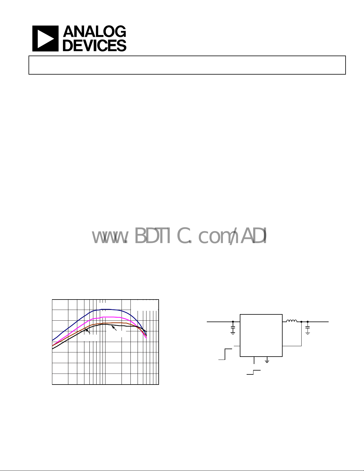
TYPICAL PERFORMANCE CHARACTERISTICS
100
95
90
85
80
75
EFFICIENCY (%)
70
65
60
10 100 1000
Rev. B
Information furnished by Analog Devices is believed to be accurate and reliable. However, no
responsibility is assumed by Anal og Devices for its use, nor for any infringements of patents or ot her
rights of third parties that may result from its use. Specifications subject to change without notice. No
license is granted by implication or otherwise under any patent or patent rights of Analog Devices.
Trademarks and registered trademarks are the property of their respective owners.
VIN = 3.6V
VIN = 2.7V
VIN = 3V
VIN = 4.2V
LOAD CURRENT (mA)
Figure 1.
V
OUT
T
A
= 1.375V
= 25°C
06631-052
TYPICAL APPLICATIONS CIRCUIT
INPUT VOLTAGE
2.7V TO 5. 5V
2.2µF
FORCED
DCM/
CCM
One Technology Way, P.O. Box 9106, Norwood, MA 02062-9106, U.S.A.
Tel: 781.329.4700 www.analog.com
Fax: 781.461.3113 ©2007 Analog Devices, Inc. All rights reserved.
C
IN
CCM
V
IN
MODE
OFF
ADP2102
EN GND
ON
LX
FB/OUT
Figure 2.
OUTPUT VO LTAGE
L
0.8V TO 1. 875V
1µH
C
2.2µF
OUT
06631-001
Page 2

ADP2102
www.BDTIC.com/ADI
TABLE OF CONTENTS
Features .............................................................................................. 1
Applications....................................................................................... 1
General Description......................................................................... 1
Typical Performance Characteristics ............................................. 1
Typical Applicat i o n s C i rc uit............................................................ 1
Revision History ............................................................................... 2
Specifications..................................................................................... 3
Absolute Maximum Ratings............................................................ 4
Thermal Resistance ...................................................................... 4
Boundary Condition .................................................................... 4
ESD Caution.................................................................................. 4
Pin Configuration and Function Descriptions............................. 5
Typical Performance Characteristics ............................................. 6
Theory of Operation ...................................................................... 13
Control Scheme .......................................................................... 13
Constant On-Time Timer......................................................... 13
Forced Continuous Conduction Mode ...................................13
Power Save Mode........................................................................ 13
Synchronous Rectification ........................................................14
Current Limit .............................................................................. 14
Soft Start...................................................................................... 15
Enable........................................................................................... 15
Undervoltage L ockout ............................................................... 15
Thermal Shutdown .................................................................... 15
Applications Information.............................................................. 16
Inductor Selection...................................................................... 16
Input Capacitor Selection.......................................................... 16
Output Capacitor Selection....................................................... 16
Typical Applicat i o n s C i rc uits .................................................... 17
Setting the Output Voltage........................................................ 19
Efficiency Considerations ......................................................... 19
Thermal Considerations............................................................ 20
Design Example.......................................................................... 20
Circuit Board Layout Recommendations ................................... 22
Recommended Layout............................................................... 22
Outline Dimensions ....................................................................... 24
Ordering Guide .......................................................................... 24
REVISION HISTORY
9/07—Rev. A to Rev. B
Changes to Features, Applications, and General Description .... 1
Changes to Table 4............................................................................ 5
Changes to Table 6.......................................................................... 17
Changes to Table 7.......................................................................... 19
Changes to Circuit Board Layout Recommendations Section.... 21
Updated Outline Dimensions....................................................... 23
Changes to Ordering Guide.......................................................... 23
6/07—Rev. 0 to Rev. A
Changes to Ordering Guide.......................................................... 23
6/07—Revision 0: Initial Version
Rev. B | Page 2 of 24
Page 3
ADP2102
www.BDTIC.com/ADI
SPECIFICATIONS
VIN = 3.6 V, EN = VIN, MODE = VIN, TA = 25°C, unless otherwise noted. Bold values indicate −40°C ≤ TA ≤ +85°C.
Table 1.
Parameter Conditions Min Typ Max Unit
INPUT CHARACTERISTICS
Input Voltage Range
2
2.7 5.5 V
Undervoltage Lockout Threshold VIN rising 2.2 2.4 2.5 V
Undervoltage Lockout Hysteresis 220 mV
OUTPUT CHARACTERISTICS
Output Voltage Range ADP2102-xx 0.8 1.875 V
Output Voltage Range ADP2102-ADJ 0.8 3.3 V
Output Voltage Initial Accuracy ADP2102-xx, TA= 25°C, I
ADP2102-xx, −40°C ≤TA ≤ 85°C, I
Load Regulation V
= 0.8 V to 1.875 V, I
OUT
Line Regulation VIN = 2.7 V to 5.5 V, I
= 0 mA
LOAD
= 0 mA
LOAD
= 0 mA to 600 mA 0.5 %
LOAD
= 10 mA 0.3 %
LOAD
−1
−2
FEEDBACK CHARACTERISTICS
FB Regulation Voltage ADP2102-ADJ
784
800
FB Bias Current ADP2102-ADJ, ADP2102-0.8
FB Impedance ADP2102-xx 375 kΩ
CURRENT CHARACTERISTICS
Operating Current ADP2102 PSM mode, I
= 0 mA 70
LOAD
Shutdown Current EN = 0 V 0.01
Output Current ADP2102, VIN = 2.7 V to 5.5 V 600 mA
LX (SWITCH NODE) CHARACTERISTICS
LX On Resistance P-channel switch, ILX = 100 mA
N-channel synchronous rectifier, ILX = 100 mA
325
200
LX Leakage Current VIN = 5.5 V, VLX = 0 V, 5.5 V
LX Minimum Off-Time ADP2102-xx, ADP2102-ADJ 100 ns
LX On-Time ADP2102-0.8
ADP2102-1.0
ADP2102-1.2
ADP2102-1.25
ADP2102-1.375
ADP2102-1.5
ADP2102-1.8
ADP2102-1.875
ADP2102-ADJ-1.2
ADP2102-ADJ-1.5
ADP2102-ADJ-1.875
ADP2102-ADJ-3.3 (VIN = 5 V)
55
70
100
103
135
150
180
190
80
155
200
198
87
107
131
133
165
182
220
237
131
177
226
238
Valley Current Limit 1 A
ENABLE, MODE CHARACTERISTICS
EN, MODE Input High Threshold
1.3
V
EN, MODE Input Low Threshold
EN, MODE Input Leakage Current VIN = 5.5 V, EN = MODE = 0 V, 5.5 V
SOFT START PERIOD
250
500
THERMAL CHARACTERISTICS
Thermal Shutdown Threshold 150 °C
Thermal Shutdown Hysteresis 15 °C
1
All limits at temperature extremes are guaranteed via correlation using standard statistical quality control (SQC).
2
The input voltage (VIN) range over which the rest of the specifications are valid. The part operates as expected until VIN goes below the UVLO threshold.
1
+1
+2
816
50
99
1
600
400
1
105
135
160
169
195
210
260
270
170
210
275
270
0.4
1
800
%
%
mV
nA
µA
µA
mΩ
mΩ
µA
ns
ns
ns
ns
ns
ns
ns
ns
ns
ns
ns
ns
V
µA
µs
Rev. B | Page 3 of 24
Page 4
ADP2102
www.BDTIC.com/ADI
ABSOLUTE MAXIMUM RATINGS
Table 2.
Parameter Rating
AVIN, EN, MODE, FB/OUT to AGND −0.3 V to +6 V
LX to PGND −0.3 V to (VIN + 0.3 V)
PVIN to PGND −0.3 V to +6 V
PGND to AGND −0.3 V to +0.3 V
AVIN to PVIN −0.3 V to +0.3 V
Operating Ambient Temperature Range −40°C to +85°C
1
Junction Temperature Range −40°C to +125°C
Storage Temperature Range −65°C to +150°C
Soldering Conditions JEDEC J-STD-020
1
The ADP2102 can be damaged when junction temperature limits are exceeded.
Monitoring ambient temperature does not guarantee that T is within the
specified temperature limits. In applications where high power dissipation
and poor thermal resistance are present, the maximum ambient temperature
may have to be derated. In applications with moderate power dissipation
and low PCB thermal resistance, the maximum ambient temperature can
exceed the maximum limit as long as the junction temperature is within
specification limits. The junction temperature (T ) of the device is dependent
on the ambient temperature (T ), the power dissipation of the device (PD),
and the junction-to-ambient thermal resistance of the package (θ ). Maximum
junction temperature (T ) is calculated from the ambient temperature (T )
and power dissipation (PD) using the formula T = T + (θ × PD).
otherwise specified, all other voltages are referenced to AGND.
A
J A
J
J A JA
J
JA
Unless
Stresses above those listed under Absolute Maximum Ratings
may cause permanent damage to the device. This is a stress
rating only; functional operation of the device at these or any
other conditions above those indicated in the operational
section of this specification is not implied. Exposure to absolute
maximum rating conditions for extended periods may affect
device reliability.
THERMAL RESISTANCE
Junction-to-ambient thermal resistance (θJA) of the package is
based on modeling and calculation using a 4-layer board. The
junction-to-ambient thermal resistance is highly dependent on
the application and board layout. In applications where high
maximum power dissipation exists, attention to thermal board
design is required. The value of θ
may vary, depending on PCB
JA
material, layout, and environmental conditions. Specified value
of θ
is based on a 4-layer, 4 in × 3 in, 2 1/2 oz copper board,
JA
as per JEDEC standards. For more information, see Application
Note
AN-772, A
Design and Manufacturing Guide for the Lead
Frame Chip Scale Package (LFCSP).
Table 3. Thermal Resistance
Package Type θ
JA
Unit
8-Lead LFCSP 54 °C/W
Maximum Power Dissipation 0.74 W
BOUNDARY CONDITION
Natural convection, 4-layer board, exposed pad soldered to PCB.
ESD CAUTION
Rev. B | Page 4 of 24
Page 5

ADP2102
www.BDTIC.com/ADI
PIN CONFIGURATION AND FUNCTION DESCRIPTIONS
1MODE
2EN
ADP2102
TOP VIEW
3FB/OUT
(Not to Scale)
4AGND
Figure 3. Pin Configuration
Table 4. Pin Function Descriptions
Pin
No. Mnemonic Description
1 MODE
2 EN
3 FB/OUT
4 AGND
5 PGND Power Ground.
6 LX
7 PVIN
8 AVIN Power Source Input. AVIN is the supply for the ADP2102 internal circuitry. This pin can be connected in three different ways.
For light-to-medium loads up to 300 mA, the AVIN pin and the PVIN pin can be shorted together.
Mode Input. To set the ADP2102 to forced continuous conduc
to power save mode/auto mode (PSM), drive MODE low.
Enable Input. Drive EN high to turn on the ADP2102. Drive EN lo
This pin cannot be left floating.
Output Sense Input or Feedback Input. F
divider. Connect OUT to the output voltage. For adjustable (no suffix) versions, FB is the input to the error amplifier.
Drive FB through a resistive voltage divider to set the output voltage. The FB regulation threshold is 0.8 V.
Analog Ground. Connect AGND to PGND at a single point as clo
electrically common with the analog ground pin.
Switch Output. LX is the drain of the P-channel MOSFET switch and
output LC filter between LX and the output voltage.
Power Source Input. Drive PVIN with a 2.7 V to 5.5 V power source. A ceramic bypass capacitor of 2.2 µF or greater is
equired on this pin to the nearest PGND plane.
r
For noise reduction, place an external RC filter bet
external RC filter are 10 Ω and 0.1 µF, respectively. This configuration can be used for all loads.
For light-to-heavy loads (greater than 300 mA), bypass the AVIN pin with a 1 pF to 0.01 µF capacitor to the
est PGND plane. Do not short the AVIN and PVIN pins when using only a bypass capacitor.
near
or fixed output versions, OUT is the top of the internal resistive voltage
8AVIN
7PVIN
6LX
5PGND
ween PVIN and AVIN. The recommended values for the
06631-003
tion mode (CCM), drive MODE high. To set the ADP2102
w to turn it off and reduce the input current to 0.1 µA.
se to the ADP2102 as possible. The exposed paddle is
the N-channel synchronous rectifier. Connect the
Rev. B | Page 5 of 24
Page 6
ADP2102
www.BDTIC.com/ADI
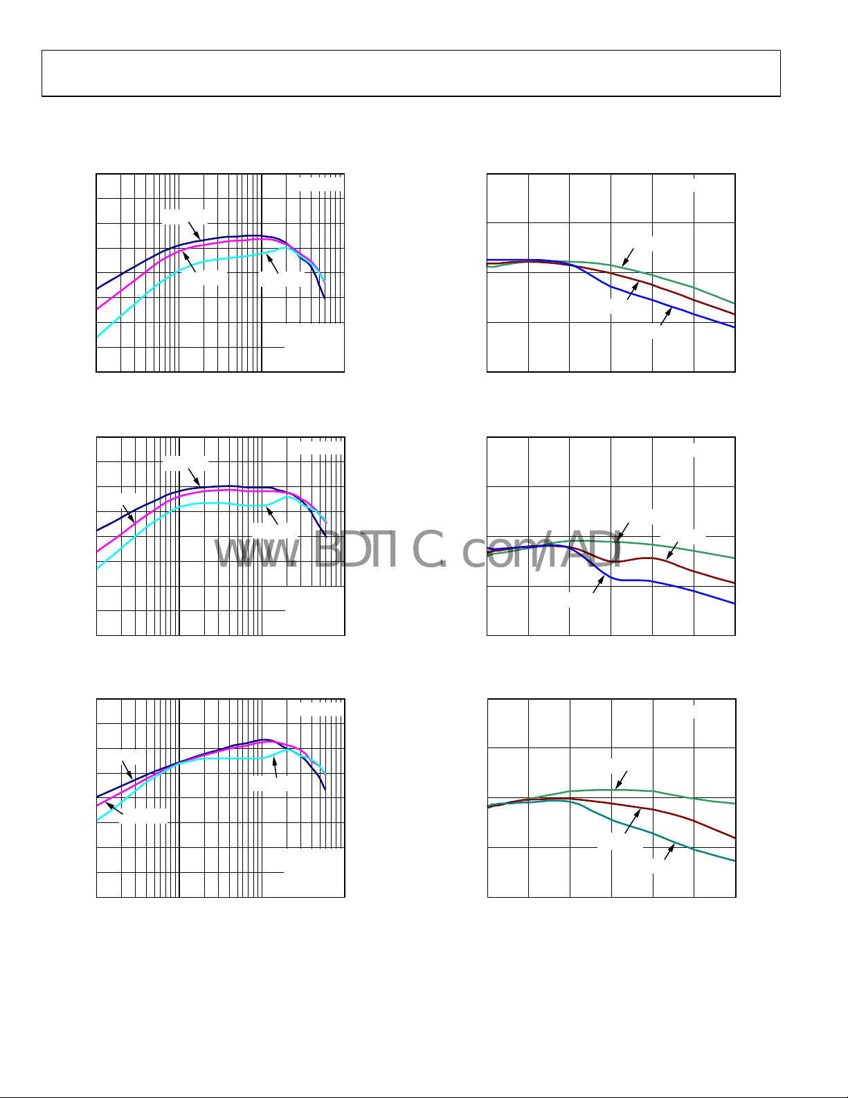
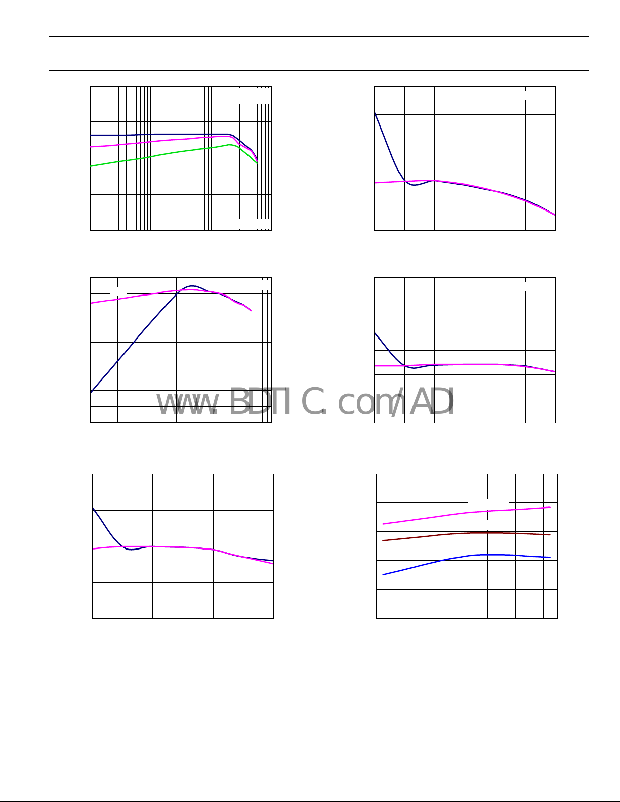
TYPICAL PERFORMANCE CHARACTERISTICS
VIN = 3.6 V, L = 2.2 µH, CIN = 2.2 µF, C
100
95
90
85
VIN = 2.7V
= 4.7 µF, unless otherwise noted.
OUT
TA = 25°C
1.22
TA = 25°C
1.21
VIN = 2.7V
80
75
EFFICIENCY (%)
70
65
60
1 10 100 1000
Figure 4. Efficiency vs. Load Current (V
100
95
90
VIN = 3.6V
85
80
75
EFFICIENCY (%)
70
65
60
1 10 100 1000
Figure 5. Efficiency vs. Load Current (V
VIN = 3.6V
LOAD CURRENT (mA)
VIN = 2.7V
LOAD CURRENT (mA)
VIN = 4.5V
OUT
VIN = 4.5V
OUT
MODE = PSM
L = 2.2µH
C
= 2.2µF
IN
C
= 10µF
OUT
= 1.2 V)
TA = 25°C
MODE = PSM
L = 2.2µH
C
= 2.2µF
IN
C
= 10µF
OUT
= 1.5 V)
1.20
OUTPUT VOLTAGE (V)
1.19
1.18
06631-004
0 100 200 300 400 500 600
Figure 7. Output Voltage Accuracy (V
1.52
1.51
1.50
OUTPUT VOLTAGE (V)
1.49
1.48
06631-005
0 100 200 300 400 500 600
Figure 8. Output Voltage Accuracy (V
VIN = 3.6V
LOAD CURRENT (mA)
VIN = 2.7V
VIN = 4.5V
LOAD CURRENT (mA)
VIN = 4.5V
OUT
VIN = 3.6V
OUT
= 1.2 V)
TA = 25°C
= 1.5 V)
06631-007
06631-020
100
95
90
VIN = 2.7V
85
80
VIN = 3.6V
75
EFFICIENCY (%)
70
65
60
1 10 100 1000
LOAD CURRENT (mA)
VIN = 4.5V
Figure 6. Efficiency vs. Load Current (V
TA = 25°C
MODE = PSM
L = 2.2µH
C
= 2.2µF
IN
C
OUT
= 1.8 V)
OUT
= 10µF
06631-006
Rev. B | Page 6 of 24
1.82
1.81
VIN = 2.7V
1.80
OUTPUT VOLTAGE (V)
1.79
1.78
0 100 200 300 400 500 600
VIN = 3.6V
VIN = 4.5V
LOAD CURRENT (mA)
Figure 9. Output Voltage Accuracy (V
= 1.8 V)
OUT
TA = 25°C
06631-009
Page 7
ADP2102
www.BDTIC.com/ADI
100
EFFICIENCY (%)
TA = 25°C
C
= 6.8pF
FF
95
90
85
VIN = 4.5V
VIN = 5.0V
VIN = 5.5V
1.53
1.52
PSM
1.51
1.50
CCM
OUTPUT VOLTAGE (V)
1.49
TA = 25°C
80
1 10 100 1000
LOAD CURRENT (mA)
Figure 10. Efficiency vs. Load Current (V
95
90
85
80
75
70
EFFICIENCY (%)
65
60
55
50
PSM
CCM
10 100 1k
LOAD CURRENT (mA)
Figure 11. PSM vs. CCM Efficiency (V
1.22
1.21
PSM
1.20
CCM
OUTPUT VOLTAGE (V)
1.19
MODE = PSM
= 3.3 V)
OUT
= 1.8 V)
OUT
TA = 25°C
TA = 25°C
1.48
06631-050
0 100 200 300 400 500 600
Figure 13. Output Voltage vs. Load Current (V
1.84
1.83
1.82
PSM
1.81
CCM
1.80
OUTPUT VOLTAGE (V)
1.79
1.78
06631-026
0 100 200 300 400 500 600
Figure 14. Output Voltage vs. Load Current (V
1.23
1.22
1.21
1.20
OUTPUT VOL TAGE (V)
1.19
LOAD CURRENT (mA)
LOAD CURRENT (mA)
I
= 300mA
LOAD
I
= 600mA
LOAD
I
LOAD
= 0mA
= 1.5 V)
OUT
TA = 25°C
= 1.8 V)
OUT
06631-013
06631-017
1.18
0 100 200 300 400 500 600
Figure 12. Output Voltage vs. Load Current (V
LOAD CURRENT (mA)
= 1.2 V)
OUT
06631-011
Rev. B | Page 7 of 24
1.18
–45 –25 –5 15 35 55 75
Figure 15. Output Voltag
TEMPERATURE ( °C)
e vs. Temperature (V
OUT
= 1.2 V)
06631-046
Page 8
ADP2102
www.BDTIC.com/ADI
1.52
1.51
1.50
I
= 0mA
LOAD
I
= 300mA
1.49
1.48
OUTPUT VOLTAGE (V)
1.47
1.46
–40 –15 10 35 60 85
Figure 16. Output Voltag
1.81
1.80
1.79
1.78
OUTPUT VOLTAGE (V)
1.77
LOAD
I
= 600mA
LOAD
TEMPERATURE ( °C)
e vs. Temperature (V
I
= 0mA
LOAD
I
= 300mA
LOAD
I
= 600mA
LOAD
= 1.5 V)
OUT
06631-047
85
80
75
70
QUIESCENT CURRENT (µA)
65
60
2.7 3.0 3.3 3.6 3.9 4.2 4.5 4.8 5.1 5.4
INPUT VOLTAGE (V)
+85°C
+25°C
–40°C
Figure 19. Quiescent Current vs. Input Voltage
77
76
75
74
73
72
QUIESCENT CURRENT (µA)
71
06631-045
1.76
–40 –15 10 35 60 85
Figure 17. Output Voltag
3.40
3.36
3.32
3.28
OUTPUT VOLTAGE (V)
3.24
3.20
0 100 200 300 400 500 600
Figure 18. Output Voltage Accuracy (V
TEMPERATURE (° C)
e vs. Temperature (V
LOAD CURRENT (mA)
+85°C
+25°C
–40°C
= 3.3 V)
OUT
OUT
= 1.8 V)
70
06631-048
–40 –20 0 20 40 60 80 100 120
TEMPERATURE (° C)
06631-053
Figure 20. Quiescent Current vs. Temperature
0.8005
0.8000
0.7995
0.7990
0.7985
0.7980
FEEDBACK VOLT AGE (V)
0.7975
0.7970
0.7965
06631-049
–50 0 50 100
TEMPERATURE ( °C)
V
= 3.6V
IN
06631-021
Figure 21. Feedback Voltage vs. Temperature
Rev. B | Page 8 of 24
Page 9

ADP2102
www.BDTIC.com/ADI
4.5
4.0
3.5
0.8V
TA = 25°C
1.25V
1.2V
1V
400
350
300
250
PMOS SWITCH
3.0
2.5
1.5V
SWITCHING FREQUENCY (MHz)
2.0
1.5
0 100 200 300 400 500 600
1.875V
1.8V
LOAD CURRENT (mA)
1.375V
Figure 22. Switching Frequency vs. Load Current
1.08
1.07
1.06
1.05
1.04
1.03
CURRENT LIMIT (A)
1.02
1.01
1.00
2.7 3.0 3.3 3. 6 3.9 4.2 4.5 4. 8 5.1 5.4 5.7
INPUT VOLTAGE (V)
TA = 25°C
Figure 23. Valley Current Limit
200
150
100
SWITCH ON RESISTANCE (mΩ)
50
0
06631-051
–40 –20 0 20 40 60 80 100 120
NMOS SWITCH
TEMPERATURE (° C)
06631-054
Figure 25. Switch On Resistance vs. Temperature
T
CH4: LX
4
1
2
06631-029
CH1: IL
CH2: V
CH1 500mA Ω
OUT
B
W
CH2 2.00V M 1.00µs A CH4 2.76V
CH4 2.00V
B
W
B
W
T 51.00%
TA = 25°C
06631-014
Figure 26. PSM Mode Operation at Very Light Loads (10 mA)
400
350
300
250
200
150
100
SWITCH ON RESISTANCE (mΩ)
50
0
2.7 3.0 3.3 3.6 3.9 4. 2 4.5 4.8 5.1 5.4
PMOS SWITCH
NMOS SWITCH
INPUT VOLTAGE (V)
TA = 25°C
Figure 24. Switch On Resistance vs. Input Voltage
06631-027
Rev. B | Page 9 of 24
T
1
3
CH1 50.0mV
CH3 50.0mA Ω
CCM
CH1: V
OUT
CH3: IL
B
W
B
W
M 100µs A CH3 86.0mA
TA = 25°C
PSMPSM
06631-022
Figure 27. PSM Mode Entry—Exit Operation (10 mA to 50 mA to 10 mA)
Page 10

ADP2102
www.BDTIC.com/ADI
T
CH4: LX
4
CH1: IL
1
CH2: V
OUT
2
CH1 500mA Ω
B
W
CH2 2.00V M 10.0µs A CH4 2.72V
CH4 2.00V
B
W
B
W
T 51.00%
Figure 28. PSM Mode Operation at Light Loads (75 mA)
TA = 25°C
06631-015
180
TA = 25°C
160
V
= 1.5V
140
120
OUT
V
OUT
= 1.375V
100
80
60
PSM THRESHOL D (mA)
40
20
L = 2.2µH
0
2.5 3.0 3.5 4.0 4.5 5.0 5.5
INPUT VOLTAGE (V)
Figure 31. Typical PSM Threshold vs. Input Voltage
06631-028
1
3
4
CH1 200mA Ω
CH3 2.00V
CH4: V
B
W
B
W
CH4 2.00V
CH1: IL
CH3: LX
T
OUT
M 200ns A CH1 388mA
B
W
T –4.00000ns
TA = 25°C
Figure 29. CCM Mode Operation at Medium/Heavy Loads (0.3 A)
OUT
T
TA = 25°C
1
VIN = 3.6V
V
= 1.5V
OUT
I
= 0mA - 75mA - 0mA
LOAD
CH1: LX
CH3: V
T
1
CH1: V
CH2: I
2
CH1 50.0mV CH2 200mA Ω M 100µs A CH2 220mA
06631-016
LOAD
B
W
(AC)
OUT
(0mA TO 300mA)
T 23.60%
Figure 32. Load Transient Response (V
T
1
CH1: V
OUT
(AC)
= 1.2 V)
OUT
TA = 25°C
TA = 25°C
06631-023
3
CH2: IL
2
0mA
CH1 2.00V CH2 100mA Ω M 200µ s A CH2 82.0mA
CH3 1. 00V
75mA
0mA
B
W
B
W
06631-031
Figure 30. Light Load Behavior
Rev. B | Page 10 of 24
2
B
CH1 50.0mV CH2 200mA Ω M 100µs A CH2 236mA
W
Figure 33. Load Transient Response (V
CH2: I
(0mA TO 300mA)
LOAD
= 1.5 V)
OUT
06631-024
Page 11

ADP2102
www.BDTIC.com/ADI
T
TA = 25°C
T
TA = 25°C
1
CH1: V
CH2: I
2
CH1 50.0mV CH2 200mA Ω M 100µs A CH2 264mA
LOAD
B
W
(AC)
OUT
(0mA TO 300mA)
T –300.000µs
Figure 34. Load Transient Response (V
T
CH1: V
OUT
1
(AC)
OUT
= 1.8 V)
TA = 25°C
CH3: VIN(3V TO 4V STEP)
3
CH1 50.0mV M 200µs A CH3 3.74V
CH3 1. 00V
B
W
B
W
Figure 35. Line Transient Response (V
= 1.2 V)
OUT
CH1: V
1
OUT
(AC)
CH3: VIN(3.6V TO 4.2V STEP)
3
CH1 50.0mV M 40.0µs A CH3 3.70V
06631-025
CH3 1. 00V
4
B
W
B
W
Figure 37. Line Transient Response (V
T
CH4: EN
= 1.8 V)
OUT
TA = 25°C
06631-044
CH1: LX
1
CH2: V
OUT
2
06631-032
CH1 200mA Ω
B
W
CH2 1.00V M 20.0ms A CH3 2. 00V
CH4 2.00V
B
W
B
W
T 14.60%
06631-019
Figure 38. Start-Up and Shutdown Waveform
T
CH1: V
1
OUT
(AC)
TA = 25°C
CH3: VIN(3V TO 4V STEP)
3
CH1 50.0mV M 100µs A CH3 3.72V
CH3 1. 00V
B
W
B
W
Figure 36. Line Transient Response (V
= 1.5 V)
OUT
06631-035
Rev. B | Page 11 of 24
T
CH1: V
IN
1
CH2: V
2
OUT
TA = 25°C
CH3: LX
3
B
CH1 2.00V CH2 500mV M 400µ s A CH1 1.40V
CH3 200mA Ω
W
B
W
B
W
T 27.60%
Figure 39. Light Load Start-Up Waveform
06631-030
Page 12

ADP2102
www.BDTIC.com/ADI
T
CH1: EN
TA = 25°C
CH1: LX
1
TA = 25°C
1
CH2: V
2
OUT
CH3: IL
3
B
CH1 2.00V CH2 500mV M 2. 00ms A CH2 350mV
CH3 200mA Ω
W
B
W
B
W
T 6.600%
Figure 40. Heavy Load Start-Up Waveform
T
CH4: V
4
OUT
(AC)
CH1: LX
1
B
CH1 2.00V M 2.00µs A CH1 4.20V
Figure 41. PSM Mode Ripple (V
W
CH4 20.00mV
B
W
T 51.00%
= 3.6 V, Load = 50 mA)
IN
TA = 25°C
L = 2.2µH
C
= 2.2µF
IN
C
= 4.7µF
OUT
CH2: V
OUT
3
CH4: IL
4
B
CH1 5.00V
06631-033
W
B
W
CH4 500mA ΩCH3 1.00V
M 1.00s A CH3 440mV
B
W
06631-018
Figure 42. Short-Circuit Response at Output
CH4 500mV
T
CH4: V
OUT
CH3: IL
M 100µs A CH4 680mV
B
W
T 43.40%
TA = 25°C
06631-055
VIN = 3.6V
V
= 1.375V
OUT
C
= 4.7µF
OUT
I
= 100mA
LOAD
4
3
B
06631-034
CH3 200mA Ω
W
Figure 43. Soft Start Waveform
Rev. B | Page 12 of 24
Page 13

ADP2102
−
www.BDTIC.com/ADI
THEORY OF OPERATION
The ADP2102 is a high frequency, synchronous step-down,
dc-to-dc converter optimized for battery-powered, portable
applications. It is based on constant on-time current-mode
control architecture with voltage feed forward to null frequency
variation with line voltage, creating a pseudofixed frequency.
This type of control allows generation of very low output voltages
a
t a higher switching frequency and offers a very fast load and
line transient response with minimal external component count
and size. The ADP2102 provides features such as undervoltage
lockout, thermal shutdown, and short-circuit protection.
The ADP2102 uses valley current-mode control, which helps to
revent minimum on-time limitations at very low output voltages.
p
This allows high frequency operation, resulting in low filter
inductor and capacitor values.
CONTROL SCHEME
The ADP2102 high-side power switch on-time is determined by
a one-shot timer whose pulse width is directly proportional to
the output voltage and inversely proportional to the input or
line voltage. Another one-shot timer sets a minimum off time to
allow for inductor valley current sensing.
The constant on-time, one-shot timer is triggered at the rising
e of EN and, subsequently, when the low-side power switch
edg
current is below the valley current limit threshold and the
minimum off-time one-shot timer has timed out.
While the constant on-time is asserted, the high-side power
tch is turned on. This causes the inductor current to ramp
swi
positively. After the constant on-time has completed, the highside power switch turns off and the low-side power switch turns
on. This causes the inductor current to ramp negatively until
the sensed current flowing in this switch has reached valley
current limit. At this point, the low-side power switch turns off
and a new cycle begins with the high-side switch turning on,
provided that the minimum off-time one shot has timed out.
CONSTANT ON-TIME TIMER
The constant on-time timer sets the high-side switch on-time.
This fast, low jitter, adjustable one shot varies the on-time in
response to input voltage for a given output voltage. The highside switch on-time is inversely proportional to the input
voltage and directly proportional to the output voltage.
= K(V
t
ON
The duty cycle for a buck converter operating in continuous
nduction mode (CCM) is given by D = V
co
definition, D = t
terms of V
OUT/VIN
= V
t
ON
OUT
) (1)
OUT/VIN
and, by
OUT/VIN
/(tON + t
ON
and tON/(tON + t
). Therefore, equating the duty cycle
OFF
) gives
OFF
/(VIN × fSW) (2)
Equating Equation 1 and Equation 2 gives
= 1/K (3)
f
SW
where K is a
n internally set on-time scale factor constant resulting
in a constant switching frequency.
As shown in Equation 1, the steady state switching frequency
i
s theoretically independent of both the input and output voltages
to a first order. This means the loop switches at a nearly constant
frequency until a load step occurs.
When a load step occurs, the constant on-time control loop
re
sponds by modulating the off time up or down to quickly
return to regulation. This momentary frequency variation
results in a faster load transient response than a fixed frequency
current-mode control loop of similar bandwidth with a similar
external filter inductor and capacitor. This is an advantage of
a constant on-time control scheme.
Resistive voltage losses in the high-side and low-side power
witches, package parasitics, inductor DCR, and board parasitic
s
resistance cause the loop to compensate by reducing the off time
and, therefore, increase the switching frequency with increasing
load current.
A minimum off-time constraint is introduced to allow inductor
val
ley current sensing on the synchronous switch.
FORCED CONTINUOUS CONDUCTION MODE
When the MODE pin is high, the ADP2102 operates in forced
continuous conduction mode (CCM). In this mode, irrespective
of the load current, the inductor current stays continuous, and
CCM is the preferred mode of operation for low noise applications.
During this mode, the switching frequency stays close to 3 MHz
typical. In this mode, efficiency is lower at light loads, compared to
the power save mode, but the output voltage ripple is minimized.
POWER SAVE MODE
When the MODE pin is low, the ADP2102 operates in power
save mode (PSM). In this mode, at light load currents, the part
automatically goes into reduced frequency operation where
some pulses are skipped to increase efficiency while remaining
in regulation. At light loads, a zero-crossing comparator
truncates the low-side switch on-time when the inductor
current becomes negative. In this condition, the part works in
discontinuous conduction mode (DCM). The threshold between
CCM and DCM is approximately
VVV
×
I
LOAD
(skip) =
IN
2
There is a first-order dependency of this threshold on the internally
s
et on-time scale factor indicated in Equation 3. For higher load
currents, the inductor current does not cross zero threshold. The
device switches to the continuous conduction mode, and the
frequency is fixed to the nominal value.
)(
OUTOUT
(4)
fVL
×××
IN
SW
Rev. B | Page 13 of 24
Page 14

ADP2102
R
−
×
www.BDTIC.com/ADI
As a result of this auto mode control technique, losses are
minimized at light loads, improving system efficiency.
The PSM reverse current comparator controls the entry and exit
to forced continuous conduction mode. Some minor jitter is
in
normal during transition from DCM to CCM with loads at
approximately 100 mA typical, and it has no adverse impact on
regulation.
SYNCHRONOUS RECTIFICATION
In addition to the P-channel MOSFET switch, the ADP2102
in
cludes an integrated N-channel MOSFET synchronous rectifier. The synchronous rectifier improves efficiency, especially
at low output voltages, and reduces cost and board space by
eliminating the need for an external rectifier.
CURRENT LIMIT
The current limit circuit employs a valley current sensing scheme.
Current limit detection occurs during the off time through
sensing of the voltage drop across the on resistance of the
synchronous rectifier switch. The detection threshold is 1 A
typical.
Figure 45 illustrates the inductor current waveform during normal
operation and during current limit. The output current, I
is the average of the inductor ripple current waveform. The
low-to-medium load current waveform illustrates the continuous
conduction mode operation with peak and valley inductor
currents below the current limit threshold. When the load
current is increased, the ripple waveform maintains the same
amplitude and frequency because the current falls below the
current limit threshold at the valley of the ripple waveform.
As the current falls below the threshold during the normal offtime of each cycle, the start of each on-time is not delayed, and
the circuit output voltage is regulated at the correct value.
OUT
,
When the load current is further increased such that the lower
peak
is above the current limit threshold, the off time is lengthened
to allow the current to decrease to this threshold before the next
on-time begins.
Both V
operates in constant current mode. The load current (I
and the switching frequency are reduced as the circuit
OUT
OCL
) under
these conditions is equal to the current limit threshold plus half
the ripple current, as shown in Equation 5 and in Figure 44.
= I
I
OCL
+ IL/2 (5)
VALLEY
DC CURRENT LIMIT = MAX LO AD
I
OCL
TIME
ΔI
06631-036
INDUCTO
CURRENT
VALLEY CURRENT LIMIT
Figure 44. Valley Current Limit
The ripple current is calculated using Equation 6.
VVV
I
OUT
=
L
IN
IN
SW
)(
OUT
(6)
LfV
××
The ADP2102 also provides a negative current limit to prevent
a
n excessive reverse inductor current when the switching section
sinks current from the load in forced continuous conduction
mode. Under negative current limit conditions, both the highside and low-side switches are disabled.
CURRENT LIMIT
THRESHOLD
I
INDUCTOR
CURRENT
OUT
MEDIUM LOAD
CURRENT
NORMAL OPERAT ION
Figure 45. Inductor Current—Current Limit Operation
Rev. B | Page 14 of 24
I
PEAK
I
OCL
I
VALLEY
ΔI
HIGH LOAD
CURRENT
CURRENT LIMI T
06631-037
Page 15

ADP2102
A
www.BDTIC.com/ADI
SOFT START
The ADP2102 has an internal soft start function that ramps the
output voltage in a controlled manner upon startup, therefore
limiting the inrush current. This prevents possible input voltage
drops when a battery or a high impedance power source is
connected to the input of the converter.
ENABLE
The device starts operation with soft start when the EN pin is
toggled from logic low to logic high. Pulling the EN pin low
forces the device into shutdown mode, with a typical shutdown
current of 0.01 µA. In shutdown mode, both the high-side and
low-side power switches are turned off, the internal resistor feedback divider is disconnected, and the entire control circuitry is
switched off. For proper operation, the device is in shutdown
mode when voltage applied to this pin is less than 0.4 V and
enabled when voltage applied is greater than 1.3 V. This pin
must not be left floating.
UVLO
THERMAL
SHUTDOWN
UNDERVOLTAGE LOCKOUT
The undervoltage lockout circuit prevents the device from
operating incorrectly at low input voltages. It prevents the
converter from turning on the main switch and the synchronous
switch under undefined conditions and, therefore, prevents
deep discharge of the battery supply.
THERMAL SHUTDOWN
When the junction temperature, TJ, exceeds 150°C typical,
the device goes into thermal shutdown. In this mode, the highside and low-side power switches are off. The device resumes
operation when the junction temperature again falls below
135°C typical.
VIN
8 1 7
PVINMODE
EN
FB/OUT
AGND
2
3
4
BANDGAP
REFERENCE
R
R
COMPENSATION
FIXED
ADJUSTABLE
RISE-
DETECT
ERROR
AMPLIFIER
INTERNAL
MIN OFF-TIMER
ON-TIME TIMER
REGULATION
COMPARATOR
CURRENT SENSE
REVERSE CURRENT
COMPARATOR
Figure 46. Internal Block Diagram
S
Q
R
AMPLIFIER
NON-
OVERLAPPING
DRIVERS
6
5
LX
PGND
06631-038
Rev. B | Page 15 of 24
Page 16

ADP2102
I
×
www.BDTIC.com/ADI
APPLICATIONS INFORMATION
The external component selection for the ADP2102 applications
circuit, as shown in Figure 2, is driven by the load requirement
and begins with the selection of Inductor L. Once the inductor
is chosen, C
and C
IN
can be selected.
OUT
INDUCTOR SELECTION
The high switching frequency of the ADP2102 allows for minimal
output voltage ripple, even with small inductors. Inductor sizing
is a trade-off between efficiency and transient response. A small
inductor leads to a larger inductor current ripple that provides
excellent transient response but degrades efficiency. Due to the
high switching frequency of the ADP2102, multilayer ceramic
inductors can be used for an overall smaller solution size. Shielded
ferrite core inductors are recommended for their low core losses
and low electromagnetic interference (EMI).
As a guideline, the inductor peak-to-peak current ripple, ΔI
,
L
is typically set to 1/3 of the maximum load current for optimal
transient response and efficiency.
ΔI
−× )(
IN
SW
OUT
≈
LfV
××
OUT
=
L
IN
)(MAXLOAD
(7)
3
VVV
)(
VVV
−×
IN
L
where f
=
IDEAL
is the switching frequency.
SW
OUT
IN
SW
OUT
3.0
IfV
×××
)(
MAXLOAD
Finally, it is important that the inductor be capable of handling
the maximum peak inductor current, I
, determined by the
PK
following equation:
= I
I
PK
LOAD(MAX)
+ ΔIL/2 (8)
The dc current rating of the inductor should be at least equal
to the maximum load current plus half the ripple current to
prevent core saturation. Table 5 shows some typical surface
mount inductors that work well in ADP2102 applications.
INPUT CAPACITOR SELECTION
The input capacitor must be able to support the maximum
input operating voltage and the maximum rms input current.
The rms input current flowing through the input capacitor is,
at maximum, I
standing the rms input current for the maximum load current
in the application to be used.
= I
I
rms
The input capacitor reduces input voltage ripple caused by the
switch currents on the PVIN pin. Place the input capacitor as
close as possible to the PVIN pin.
/2. Select an input capacitor capable of with-
OUT
VVV )( −×
IN
OUTMAX
×
OUT
V
OUT
IN
(9)
In principle, different types of capacitors can be considered, but
for battery-powered applications, the best choice is a multilayer
ceramic capacitor, due to its small size and equivalent series
resistance (ESR).
It is recommended that the PVIN pin be bypassed with a 2.2 μF
or larger ceramic input capacitor. The size of the input capacitor
can be increased without any limit for better input voltage filtering.
X5R or X7R dielectrics are recommended, with a voltage rating of
6.3 V or 10 V. Y5U and Z5U dielectrics are not recommended,
due to their poor temperature and dc bias characteristics.
In applications with greater than 300 mA load current, a ceramic
bypass capacitor of 0.01 μF is recommended on the AVIN pin
for better regulation performance.
OUTPUT CAPACITOR SELECTION
The output capacitor selection affects both the output voltage
ripple and the loop dynamics of the converter. For a given loop
crossover frequency (the frequency at which the loop gain drops
to 0 dB), the maximum voltage transient excursion (overshoot) is
inversely proportional to the value of the output capacitor. The
ADP2102 is designed to operate with small ceramic capacitors that
have low ESR and equivalent series inductance (ESL) and are thus
comfortably able to meet tight output voltage ripple specifications.
X5R or X7R dielectrics are recommended with a voltage rating of
6.3 V or 10 V. Y5V and Z5U dielectrics are not recommended,
due to their poor temperature and dc bias characteristics. When
choosing output capacitors, it is also important to account for the
loss of capacitance due to output voltage dc bias. If ceramic output
capacitors are used, the capacitor rms ripple current rating
should always meet the application requirements. The rms ripple
current is calculated as
VVV
)(
I
rms(COUT)
=
1
OUT
×
32
At nominal load currents, the converter operates in forced
continuous conduction mode, and the overall output voltage ripple
is the sum of the voltage spike caused by the output capacitor ESR
plus the voltage ripple caused by charging and discharging the
output capacitor.
= ΔIL × (ESR + 1/ (8 × C
ΔV
OUT
The largest voltage ripple occurs at the highest input voltage,
. At light load currents, the converter operates in power save
V
IN
mode, and the output voltage ripple is dependent on the output
capacitor value. The ADP2102 control loop is stable with a ceramic
output capacitor of 2.2 μF. For better transient performance, a 10 μF
ceramic capacitor is recommended at the output. Table 6 lists input
and output MLCC capacitors recommended for ADP2102
applications.
−
MAXIN
_
××
OUT
OUT
VfL
_
(10)
MAXINSW
× fSW)) (11)
Page 16 of 24
Page 17

ADP2102
V
V
www.BDTIC.com/ADI
Table 5. Recommended Inductor Selection
Manufacturer Series Value (μH) DCR (Ω) Current Rating (mA) Size (L × W × H) (mm)
FDK Corporation MIPF2520D 2.2 0.08 1300 2.5 × 2.0 × 1.0
TDK MLP2520S2R2L 2.2 0.08 1300 2.5 × 2.0 × 1.0
Murata LQM2HPN2R2MJ0 2.2 0.13 1000
Coilcraft, Inc. LPS3015-222ML 2.2 0.11 1500
Taiyo Yuden NR3010T2R2M 2.2 0.10 1100 3.0 × 3.0 × 1.0
Table 6. Recommended Input and Output Capacitor Selection
Capacitor Murata Taiyo Yuden TDK Vishay
2.2 F 6.3 V
GRM188R60J225K JMK107BJ225KA C1608X5R0J225M
X5R 0603
4.7 F 6.3 V
GRM188R60J475K JMK107BJ475KA C1608X5R0J475M
X5R 0603
10 F 6.3 V
GRM188R60J106M JMK107BJ106MA C2012X5R0J106M
X5R 0603
0.01 F 25 V
GRM155R71E103KA01D TMK105BJ103KV-F C1005X7R1E103K
X7R 0402
1 pF 50 V
GJM1554C1H1R0JB01C
X7R 0402
6.8 pF 25 V
VJ0402A6R8KXAA
X7R 0402
2.5 × 2.0 × 1.1
2.9 × 2.9 × 1.5
VJ0402A1R2CXACW1BC
TYPICAL APPLICATIONS CIRCUITS
ADP2102-FXD
1
MODE
2
EN
3
FB/OUT
4
AGND
ADP2102-FXD
1
MODE
2
EN
3
FB/OUT
4
AGND
8
AVIN
7
PVIN
6
LX
PGND
L1
2.2µH
5
C
OUT
2.2µF
Figure 47. ADP2102-FXD (0 mA ≤ I
8
AVIN
7
PVIN
2.2µH
C
BP
0.01µF
L1
PGND
6
LX
5
C
OUT
4.7µF
INPUT VO LTAGE = 2.7V TO 5.5V
V
OUTPUT VOLTAGE = 0.8V TO 1.875V
C
IN
2.2µF
≤ 300 mA)
LOAD
INPUT VO LTAGE = 2.7V TO 5.5V
V
OUT
OUTPUT VOLTAGE = 0.8V TO 1.875V
C
IN
2.2µF
GND
IN
OUT
GND
IN
6631-039
Figure 48. ADP2102-FXD (0 mA ≤ I
Rev. B | Page 17 of 24
≤ 600 mA)
LOAD
06631-008
Page 18

ADP2102
V
V
www.BDTIC.com/ADI
IN
ADP2102-ADJ
1
MODE
2
EN
3
FB/OUT
4
AGND
C
FF
*
R1
R2
NOTE
*C
IS NEEDED FOR ADJUSTABLE V
FF
SEE TABLE 7 F OR ADJUSTABLE V
AVIN
PVIN
PGND
8
7
L1
6
LX
2.2µH
5
C
4.7µF
C
OUT
2.2µF
> 1.875V ONL Y.
OUT
CONFIGURAT IONS.
OUT
Figure 49. ADP2102-ADJ (0 mA ≤ I
INPUT VOLTAGE = 2.7V TO 5.5V
V
OUTPUT VOLTAGE = 0.8V TO 3.3V
IN
GND
≤ 300 mA)
LOAD
OUT
06631-040
IN
ADP2102-ADJ
1
MODE
2
EN
3
FB/OUT
4
AGND
C
FF
*
R1
R2
NOTE
IS NEEDED FO R ADJUSTABLE V
*C
FF
SEE TABLE 7 F OR ADJUSTABLE V
AVIN
PVIN
PGND
8
7
6
LX
5
L1
2.2µH
C
BP
0.01µF
C
OUT
4.7µF
> 1.875V ONLY .
OUT
CONFIGURAT IONS.
OUT
Figure 50. ADP2102-ADJ (0 mA ≤ I
INPUT VO LTAGE = 2.7V TO 5.5V
V
OUT
OUTPUT VOLTAG E = 0.8V T O 3.3V
C
IN
2.2µF
≤ 600 mA)
LOAD
GND
06631-012
Rev. B | Page 18 of 24
Page 19

ADP2102
www.BDTIC.com/ADI
SETTING THE OUTPUT VOLTAGE
The output voltage of the ADP2102-ADJ is externally set by
a resistive voltage divider from the output voltage to FB. The ratio
of the resistive voltage divider sets the output voltage, and the
absolute value of those resistors sets the divider string current. For
lower divider string currents, the small 10 nA (50 nA maximum)
FB bias current should be taken into account when calculating
resistor values. The FB bias current can be ignored for a higher
divider string current, but doing so degrades the efficiency at very
light loads.
For the ADP2102-ADJ, the equation for output voltage selection is
= VFB (1 + R1/R2) (12)
V
OUT
where:
is the output voltage.
V
OUT
V
is the feedback voltage, 0.8 V.
FB
is the feedback resistor from V
R
1
R
is the feedback resistor from FB to GND.
2
For any adjustable output voltage greater than 1.875 V, a feed-
rward capacitor must be added across R1 for better transient
fo
performance and stability. The formula for calculation of C1 is
= 1/(2π × R1 × fCO/2) (13)
C
FF
For example, in a 5 V to 3.3 V application, if a 4.7 µF capacitor
s used at the output, a 6.8 pF feed-forward capacitor is recom-
i
mended. The output capacitor value dictates the loop crossover
frequency, f
. For an output capacitor of 4.7 µF, the loop crossover
CO
frequency is 150 kHz.
The high frequency zero created by C
important for transient load applications. Capacitor C
phase lead and functions as a speed-up capacitor to output
voltage changes, so it tends to short out R1 and improve the high
frequency response. This zero tends to produce a positive-going
bump in the phase plot. Ideally, the peak of this bump is centered
over the crossover frequency of the loop. The R1 and C
located at
f
= 1/(2π × R1 × CFF) (14)
Z
The ADP2102-xx (where xx represents the fixed output voltage)
in
cludes the resistive voltage divider internally, reducing the
external circuitry required. For improved load regulation, connect
the FB/OUT to the output voltage as close as possible to the load.
For more information about the ADP2102-ADJ configurations
fo
r V
OUT
, see Tab l e 7 .
to FB.
OUT
and R1 can be very
FF
provides
FF
zero is
FF
Table 7. ADP2102-ADJ Configurations for V
V
OUT
(V)
R1
(kΩ)
0.8 1 80.6 None 2.2 2.2 4.7
1.0 20 100 None 2.2 2.2 4.7
1.2 49.9 100 None 2.2 2.2 4.7
1.25 56.2 100 None 2.2 2.2 4.7
1.375 71.5 100 None 2.2 2.2 4.7
1.5 88.7 100 None 2.2 2.2 4.7
1.8 124 100 None 2.2 2.2 4.7
1.875 133 100 None 2.2 2.2 4.7
2.0 150 100 15 2.2 2.2 4.7
2.5 215 100 10 2.2 2.2 4.7
3.0 274 100 8.2 2.2 2.2 4.7
3.3 316 100 6.8 2.2 2.2 4.7
EFFICIENCY CONSIDERATIONS
Efficiency is defined as the ratio of output power to input power.
The high efficiency of the ADP2102 has two distinct advantages.
First, only a small amount of power is lost in the dc-to-dc converter
package that reduces thermal constraints. In addition, high efficiency delivers the maximum output power for the given input
power, extending battery life in portable applications.
Following are the four major sources of power loss in dc-to-dc
onverters like the ADP2102:
c
• Power switch conduction losses
• Inductor losses
• Switching losses
• Transition losses
Power Switch Conduction Losses
Power switch conduction losses are caused by the flow of output
current through the P-channel power switch and the N-channel
synchronous rectifier, which have internal resistances (R
associated with them. The amount of power loss can be approximated by
P
SW_COND
where D = V
The internal resistance of the power switches increases with
emperature but decreases with higher input voltage. Figure 24
t
he Typical Performance Characteristics section shows the
in t
change in R
in R
vs. temperature for both power devices.
DS (ON)
R2
(kΩ)
= (R
DS (ON)_P
.
OUT/VIN
vs. input voltage, and Figure 25 shows the change
DS (ON)
C
FF
(pF) L (μH)
× D + R
DS (ON)_N
OUT
CIN
(μF)
× (1 − D)) × I
C
(μF)
DS(ON)
2
(15)
OUT
OUT
)
Rev. B | Page 19 of 24
Page 20

ADP2102
−
×
−
×
www.BDTIC.com/ADI
Inductor Losses
Inductor conduction losses are caused by the flow of current
through the inductor, which has an internal resistance (DCR)
associated with it. Larger sized inductors have smaller DCR,
which may decrease inductor conduction losses.
Inductor core losses are related to the magnetic permeability
f the core material. Because the ADP2102 is a high switching
o
frequency dc-to-dc converter, shielded ferrite core material is
recommended for its low core losses and low EMI.
The total amount of inductor power loss can be calculated by
P
= DCR × I
L
2
+ Core Losses (16)
OUT
Switching Losses
Switching losses are associated with the current drawn by the
driver to turn on and turn off the power devices at the switching
frequency. Each time a power device gate is turned on and
turned off, the driver transfers a charge Q from the input
supply to the gate and then from the gate to ground.
The amount of power loss can be calculated by
P
SW
= (C
GATE_P
+ C
GATE_N
) × V
2
× f
IN
SW
(17)
where:
C
is the gate capacitance of the internal high-side switch.
GATE_P
is the gate capacitance of the internal low-side switch.
C
GATE_N
f
is the switching frequency.
SW
Transition Losses
Transition losses occur because the P-channel switch cannot
turn on or turn off instantaneously. In the middle of an LX node
transition, the power switch provides all the inductor current.
The source to drain voltage of the power switch is half the input
voltage, resulting in power loss. Transition losses increase with
load current and input voltage and occur twice for each
switching cycle.
The amount of power loss can be calculated by
P
= VIN/2 × I
TRAN
× (tR + tF) × f
OUT
SW
(18)
where:
is the rise time of the LX node.
t
R
t
is the fall time of the LX node.
F
THERMAL CONSIDERATIONS
In most applications, the ADP2102 does not dissipate a lot of
heat, due to its high efficiency. However, in applications with
maximum loads at high ambient temperature, low supply voltage,
and high duty cycle, the heat dissipated in the package is great
enough that it may cause the junction temperature of the die to
exceed the maximum junction temperature of 125°C. Once the
junction temperature exceeds 150°C, the converter goes into
thermal shutdown. It recovers only after the junction temperature
has decreased to below 135°C to prevent any permanent damage.
Therefore, thermal analysis for the chosen application solution is
very important to guarantee reliable performance over all
conditions.
The junction temperature of the die is the sum of the ambient
t
emperature of the environment and the temperature rise of the
package due to power dissipation, shown in the following equation:
= TA + TR (19)
T
J
where:
is the junction temperature.
T
J
T
is the ambient temperature.
A
is the rise in temperature of the package due to power
T
R
dissipation in it.
The rise in temperature of the package is directly proportional
t
o the power dissipation in the package. The proportionality
constant for this relationship is defined as the thermal resistance
from the junction of the die to the ambient temperature, as shown
in the following equation:
T
= θJA × PD (20)
R
where:
T
is the rise in temperature of the package.
R
is the thermal resistance from the junction of the die to the
θ
JA
ambient temperature of the package.
is the power dissipation in the package.
P
D
DESIGN EXAMPLE
The calculations in this section provide only a rough estimate
and are no substitute for bench evaluation.
Consider an application where the ADP2102 is used to step
d
own from 3.6 V to 1.8 V with an input voltage range of 2.7 V
to 4.2 V.
= 1.8 V @ 600 mA
V
OUT
Pulsed Load = 300 mA
V
= 2.7 V to 4.2 V (3.6 V typical)
IN
fSW = 3 MHz (typical)
= 85°C
T
A
Inductor
I
)(
VVV
IN
IL =
L =
OUT
IN
SW
OUT
≈
LfV
××
SW
)/1(
VVV
INMAX
OUTOUT
3.0
If
××
=
)(
MAXLOAD
1.90 µH
Choose a 2.2 µH inductor for this application.
I
= I
PK
LOAD(MAX)
P
= I
L
OUTMAX
(0.6 A)
+ IL/2 = 0.6 + 0.2/2 = 0.7 A
2
× DCR =
2
× 0.08 Ω (FDK MIPF2520D) = 29 mW
)(MAXLOAD
= 0.6/3 = 200 mA
3
−×
6
)2.4/8.11(8.1
=
)6.03.0103(
×××
Rev. B | Page 20 of 24
Page 21

ADP2102
www.BDTIC.com/ADI
Output Capacitor
For transient applications, assume a droop of 0.1 V. Typically,
it takes two to three cycles for the output to settle from a load
transient because the capacitor alone supplies the load current
until the loop responds.
Under these conditions, a minimum required output
pacitance is calculated as follows:
ca
×
C
OUT_MIN
= 3 ×
Δ
I
LOAD
=
fV
×
SWDROOP
××
3.03
1031.0
= 3 µF
6
Choose a 4.7 µF capacitor for this application.
For an instantaneous step decrease in load current, the output
ca
pacitor required to limit the output voltage overshoot (V
)
OS
during a full load to no load transient must be determined. This
transient requires the excess energy stored in the output inductor
to be absorbed by the output capacitor with a limited overshoot
in the output voltage.
Assuming an overshoot of 50 mV for a full load transient,
2
IL−+×
C
=
OUT
OUT
OUT
2
)(
OS
=
2
VVV
OUT
2
)6.0(H2.2
×μ
= 4.33 µF
22
)8.1()85.1(
−
Choose a 4.7 µF capacitor for this application.
VVV
)(
1
I
=
rms
1
OUT
×
32
×
32
−
−×
_
MAXIN
OUT
)8.12.4(8.1
66
××××
=
= 45 mA rms
2.4103102.2
VfL
××
MAXINSW
_
−×
Input Capacitor
Assume an input ripple of 27 mV based on 1% of V
IN_MIN.
For ceramic capacitors, the typical ESR is from 5 mΩ to 15 m.
OUT
1
1
×××−
fESRIV ××−Δ 4)/(
6
1034)005.06.0/027.0(
=
SW
= 2.2 µF
=
C
IN
I
rms
P
CIN
IN
= I
/2 = 0.3 A rms
OUT
2
= I
× ESR = (0.3)2 × 0.005 = 450 µW
rms
Losses
P
(0.310 × 0.5 + 0.145 × 0.5) × (0.6)
P
SW_COND
= (VIN/2) × I
TRAN
= (R
× D + R
DS (ON)_P
× (tR + tF) × fSW =
OUT
DS (ON)_N
2
(3.6/2) × 0.6 × (5 ns + 5 ns) × 3 × 10
P
= (C
SW
2
× 3 × 106 = 7.8 mW
(3.6)
= DCR × I
P
L
P
= P
LOSS
GATE_P
OUT
SW_COND
+ C
GATE_N
2
= 0.08 × (0.6)2 = 28.8 mW
+ P
TRAN
2
) × V
× fSW = (200 pF) ×
IN
+ PSW + PL =
× (1 − D)) × I
= 82 mW
6
= 32.4 mW
OUT
2
=
82 mW + 32.4 mW + 7.8 mW + 28.8 mW = 151 mW
= TA + θ
T
JMAX
P
= 85°C + 54°C/W × 151 mW = 93.15°C
LOSS
is well below the junction temperature maximum of 125°C.
P
LOSS
JA
P
COUT
2
= I
× ESR = (0.045)2 × 0.005 = 10.12 µW
rms
Rev. B | Page 21 of 24
Page 22

ADP2102
www.BDTIC.com/ADI
CIRCUIT BOARD LAYOUT RECOMMENDATIONS
Good circuit board layout is essential in obtaining the best
performance from the ADP2102. Poor circuit layout degrades
the output ripple and regulation, as well as the EMI and
electromagnetic compatibility performance.
Figure 52 and Figure 53 show the ideal circuit board layout for
t
he typical applications circuit shown in Figure 48. Use this
yout to achieve the highest performance. Refer to the following
la
guidelines for optimum layout:
•
Use separate analog and power ground planes. Connect the
ground reference of sensitive analog circuitry, such as output
voltage divider components, to analog ground. In addition,
connect the ground references of power components, such as
input and output capacitors, to power ground. Connect both
ground planes to the exposed pad of the ADP2102.
•
Place the input capacitor as close to the PVIN pin as possible
and connect the other end to the closest power ground plane.
•
For low noise and better transient performance, a filter is
recommended between PVIN and AVIN. Place the 0.1 F,
10 low-pass input filter between the AVIN pin and the
PVIN pin, as close to AVIN as possible; or the AVIN pin can
be bypassed with a ≥1 pF capacitor to the nearest GND plane.
RECOMMENDED LAYOUT
•
Ensure that the high current loops are as short and as wide
as possible. Make the high current path from C
, and the PGND plane back to CIN as short as possible.
C
OUT
through L,
IN
To accomplish this, ensure that the input and output capacitors
share a common PGND plane. In addition, make the high
current path from the PGND pin through L and C
OUT
back
to the PGND plane as short as possible. To do this, ensure
that the PGND pin of the ADP2102 is tied to the PGND
plane as close as possible to the input and output capacitors.
Place the feedback resistor divider network as close as possible
•
to the FB pin to prevent noise pickup. Try to minimize the
length of trace connecting the top of the feedback resistor
divider to the output while keeping away from the high
current traces and the switch node (LX) that can lead to
noise pickup. To reduce noise pickup, place an analog ground
plane on either side of the FB trace and make it as small as
possible to reduce the parasitic capacitance pickup.
MODE
EN
FB/OUT
VIN
9 mm
CBP
AGND
Figure 51. Recommended PCB Layout of the ADP2102-FXD
ADP2102
CIN
L1
COUT
INDUCTOR
PGND
8 mm
VOUT
06631-041
Rev. B | Page 22 of 24
Page 23

ADP2102
www.BDTIC.com/ADI
VIN
MODE
EN
FB/OUT
AGND
Figure 52. Recommended Layout of the Top Lay
CBP
ADP2102
CIN
L1
er of the ADP2102-FXD Application Board
PGND
COUT
INDUCTOR
VOUT
06631-042
VIN
PGNDMODE
EN
VOUT
AGND
FB/OUT
06631-043
Figure 53. Recommended Layout of the Bottom L
ayer of the ADP2102-FXD Application Board
Rev. B | Page 23 of 24
Page 24

ADP2102
www.BDTIC.com/ADI
OUTLINE DIMENSIONS
3.25
3.00 SQ
2.75
2.95
INDICATOR
0.90 MAX
0.85 NOM
SEATING
PLANE
PIN 1
12° MAX
TOP
VIEW
0.70 MAX
0.65TYP
0.30
0.23
0.18
2.75 SQ
2.55
0.05 MAX
0.01 NOM
0.20 REF
Figure 54. 8-Lead Lead Frame Chip Scale Package [LFCSP_VD]
3 mm × 3 mm Body, Very Thin, Dual Lead
Dimensions shown in millimeters
ORDERING GUIDE
Output
Model
Current (mA)
ADP2102YCPZ-0.8-R71 600 −40°C to +85°C 0.8 V 8-Lead LFCSP_VD CP-8-2 L5T
ADP2102YCPZ-1.0-R71 600 −40°C to +85°C 1.0 V 8-Lead LFCSP_VD CP-8-2 L5U
ADP2102YCPZ-1.2-R71 600 −40°C to +85°C 1.2 V 8-Lead LFCSP_VD CP-8-2 L5V
ADP2102YCPZ-1.25R71 600 −40°C to +85°C 1.25 V 8-Lead LFCSP_VD CP-8-2 L5W
ADP2102YCPZ-1.37R71 600 −40°C to +85°C 1.375 V 8-Lead LFCSP_VD CP-8-2 L5X
ADP2102YCPZ-1.5-R71 600 −40°C to +85°C 1.5 V 8-Lead LFCSP_VD CP-8-2 L5Y
ADP2102YCPZ-1.8-R71 600 −40°C to +85°C 1.8 V 8-Lead LFCSP_VD CP-8-2 L5Z
ADP2102YCPZ-1.87R71 600 −40°C to +85°C 1.875 V 8-Lead LFCSP_VD CP-8-2 L60
ADP2102YCPZ-1-R7
1
600 −40°C to +85°C 0.8 V to 1.2 V 8-Lead LFCSP_VD CP-8-2 L6K
ADP2102YCPZ-2-R71 600 −40°C to +85°C 1.2 V to 1.5 V 8-Lead LFCSP_VD CP-8-2 L6L
ADP2102YCPZ-3-R7
1
600 −40°C to +85°C 1.5 V to 1.875 V 8-Lead LFCSP_VD CP-8-2 L6M
ADP2102YCPZ-4-R71 600 −40°C to +85°C 2.5 V to 3.3 V2 8-Lead LFCSP_VD CP-8-2 L6N
ADP2102-0.8-EVALZ1 Fixed Output 0.8 V Evaluation Board
ADP2102-1.0-EVALZ1 Fixed Output 1.0 V Evaluation Board
ADP2102-1.2-EVALZ1 Fixed Output 1.2 V Evaluation Board
ADP2102-1.25-EVALZ1 Fixed Output 1.25 V Evaluation Board
ADP2102-1.375-EVALZ1 Fixed Output 1.375 V Evaluation Board
ADP2102-1.5-EVALZ1 Fixed Output 1.5 V Evaluation Board
ADP2102-1.8-EVALZ1 Fixed Output 1.8 V Evaluation Board
ADP2102-1.875EVALZ1 Fixed Output 1.875 V Evaluation Board
ADP2102-1-EVALZ1 Adjustable Output 0.8 V to 1.2 V Evaluation Board
ADP2102-2-EVALZ1 Adjustable Output 1.2 V to 1.5 V Evaluation Board
ADP2102-3-EVALZ1 Adjustable Output 1.5 V to1.875 V Evaluation Board
ADP2102-4-EVALZ1 Adjustable Output 2.5 V to 3.3 V Evaluation Board
1
Z = RoHS Compliant Part.
2
2.5 V to 3.3 V adjustable output voltage option is from 4.5 V < VIN < 5.5 V only.
3
Operating junction temperature range: −40°C to +125°C.
Temperature
3
Range
Output
Voltage
0.60 MAX
0.50
0.40
0.30
(CP-8-2)
0.60 MAX
5
EXPOSED
PAD
(BOTT OM VIEW)
4
0.50
BSC
8
1.60
1.45
1.30
1
1.89
1.74
1.59
PIN 1
INDICATOR
Package
Description
61507-B
Package
Option
Branding
©2007 Analog Devices, Inc. All rights reserved. Trademarks and
registered trademarks are the property of their respective owners.
D06631-0-9/07(B)
Rev. B | Page 24 of 24
 Loading...