

Page 1
Logic Controlled, 1 A, High-Side Load
Switch with Reverse Current Blocking
Data Sheet
FEATURES
Low RDSON of 50 mΩ @ 3.3 V (WLCSP only)
Low input voltage range: 1.65 V to 6.5 V
1 A continuous operating current
Built-in level shift for control logic that can be operated by
1.2 V logic
Low 2.5 μA quiescent current @ V
Low 1.1 μA shutdown current @ V
Reverse current blocking
Programmable start-up time
Ultrasmall 1 mm × 1 mm, 4-ball, 0.5 mm pitch (WLCSP)
Tiny 8-lead lead frame chip scale package (LFCSP)
2.0 mm × 2.0 mm × 0.55 mm, 0.5 mm pitch
APPLICATIONS
Mobile phones
Digital cameras and audio devices
Portable and battery-powered equipment
= 2.8 V
IN
= 2.8 V
IN
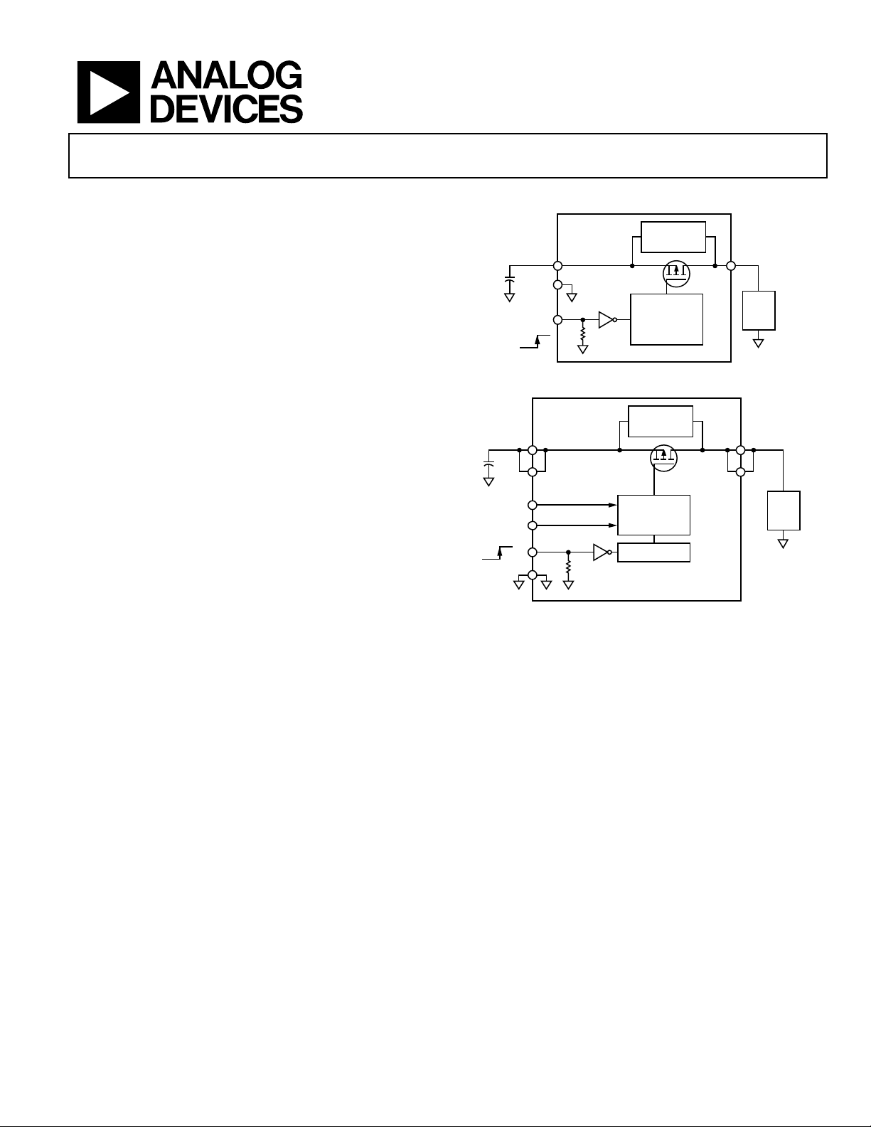
TYPICAL APPLICATION CIRCUITS
ADP198
VIN
+
GND
EN
ON
OFF
Figure 1. WLCSP
ADP198
VIN
+
VIN VOUT
SEL0
SEL1
ON
EN
OFF
GND
REVERSE
POLARITY
PROTECTION
LEVEL SHIFT
AND SLEW
RATE CONTROL
REVERSE
POLARITY
PROTECTION
SLEW
RATE CONTROL
LEVEL SHIFT
ADP198
VOUT
LOAD
09484-001
VOUT
LOAD
GENERAL DESCRIPTION
The ADP198 is a high-side load switch designed for operation
between 1.65 V and 6.5 V that is protected against reverse
current flow from output to input. A load switch provides power
domain isolation, thereby helping to keep subsystems isolated and
powered independently and enabling reduced power consumption.
The ADP198 contains a low on-resistance P-channel MOSFET
that supports more than 1 A of continuous load current. The
low 2.5 μA quiescent current and ultralow shutdown current
make the ADP198 ideal for battery-operated portable
Figure 2. LFCSP
equipment. The built-in level shifter for enable logic makes the
ADP198 compatible with modern processors and general-purpose
input/output (GPIO) controllers. The LFCSP version also allows
the user to program the start-up time to control the inrush
current at turn on.
The ADP198 is available in an ultrasmall 1 mm × 1 mm, 4-ball,
0.5 mm pitch WLCSP. An 8-lead, 2 mm × 2 mm × 0.55 mm,
0.5 mm pitch LFCSP is also available.
09484-002
Rev. D
Information furnished by Analog Devices is believed to be accurate and reliable. However, no
responsibility is assumed by Analog Devices for its use, nor for any infringements of patents or other
rights of third parties that may result from its use. Specifications subject to change without notice. No
license is granted by implication or otherwise under any patent or patent rights of Analog Devices.
Trademarks and registered trademarks are the property of their respective owners.
One Technology Way, P.O. Box 9106, Norwood, MA 02062-9106, U.S.A.
Tel: 781.329.4700 www.analog.com
Fax: 781.461.3113 ©2011–2012 Analog Devices, Inc. All rights reserved.
Page 2

ADP198 Data Sheet
TABLE OF CONTENTS
Features .............................................................................................. 1
Applications ....................................................................................... 1
Typical Application Circuits ............................................................ 1
General Description ......................................................................... 1
Revision History ............................................................................... 2
Specifications ..................................................................................... 3
Absolute Maximum Ratings ....................................................... 5
Thermal Data ................................................................................ 5
Thermal Resistance ...................................................................... 5
ESD Caution .................................................................................. 5
Pin Configurations and Function Descriptions ........................... 6
REVISION HISTORY
6/12—Rev. C to Rev. D
Changes to Table Headings in Table 6 ......................................... 14
Added Text to Diode OR’ing Applications Section .................... 15
Updated Outline Dimensions ....................................................... 16
4/12—Rev. B to Rev. C
Changes to VOUT Time Parameters ............................................. 3
11/11—Rev. A to Rev. B
Changes to WLCSP Turn-On Delay Time Parameter ................. 3
Changes to Ordering Guide .......................................................... 16
10/11—Rev. 0 to Rev. A
Change to Features Section ............................................................. 1
Changes to Table 1, Specifications Section ................................... 3
Change to Ground Current Section ............................................. 12
Changes to Enable Feature Section .............................................. 13
Updated Outline Dimensions ....................................................... 16
10/11—Revision 0: Initial Version
Typical Performance Characteristics ..............................................8
Theory of Operation ...................................................................... 11
Applications Information .............................................................. 12
Ground Current .......................................................................... 12
Enable Feature ............................................................................ 13
Timing.......................................................................................... 14
Diode OR’ing Applications ....................................................... 15
Packaging and Ordering Information ......................................... 16
Outline Dimensions ................................................................... 16
Ordering Guide .......................................................................... 16
Rev. D | Page 2 of 16
Page 3

Data Sheet ADP198
High
VIH
VIN ≤ 5 V, TJ = −40°C to +85°C
1.2
V
VIN = 1.65 V, I
= 200 mA, VEN = 1.5 V
180 mΩ
VIN = 1.65 V, I
= 200 mA, VEN = 1.5 V
200 mΩ
VIN = 3.6 V, I
= 200 mA, VEN = 1.5 V, C
= 1 μF; SEL0 = H, SEL1 = H
1100
μs
SPECIFICATIONS
VIN = 2.8 V, EN = VIN, I
Table 1.
Parameter Symbol Test Conditions/Comments Min Typ Max Unit
INPUT VOLTAGE RANGE VIN TJ = −40°C to +85°C 1.65 6.5 V
EN INPUT
Threshold
5 V < VIN, TJ = −40°C to +85°C 1.3 V
Low VIL 1.65 V ≤ VIN ≤ 6.5 V, TJ = −40°C to +85°C 0.43 V
Pull-Down Current IEN 500 nA
REVERSE BLOCKING
V
Current VEN = 0, VIN = 0, V
OUT
VEN = 0, VIN = 0, V
Hysteresis |VIN − V
CURRENT
Quiescent Current IQ I
VIN = V
VIN = V
Off State Current I
EN = GND, TJ = −40°C to +85°C 2 µA
EN = GND, V
VIN to VOUT RESISTANCE RDSON
WLCSP VIN = 5 V, I
VIN = 3.3 V, I
VIN = 2.8 V, I
VIN = 1.8 V, I
LFCSP VIN = 5 V, I
VIN = 3.3 V, I
VIN = 2.8 V, I
VIN = 1.8 V, I
VOUT TIME
WLCSP
Turn-On Delay Time t
ADP198ACBZ-11-R7 VIN = 3.6 V, I
LFCSP
Turn-On Delay Time t
VIN = 3.6 V, I
VIN = 3.6 V, I
= 200 mA, TA = 25°C, unless otherwise noted.
OUT
= 6.5 V 7 µA
OUT
= 6.5 V, TJ = −40°C to +85°C 13 µA
OUT
| 75 mV
OUT
= 0 mA, TJ = −40°C to +85°C, includes EN pull-down current
OUT
= 2.8 V 2.5 µA
OUT
= 6.5 V 20 µA
OUT
EN = GND 1.1 µA
OFF
= 0 V, TJ = −40°C to +85°C 2 µA
OUT
= 200 mA, VEN = 1.5 V 40 mΩ
LOAD
= 200 mA, VEN = 1.5 V 50 80 mΩ
LOAD
= 200 mA, VEN = 1.5 V 60 mΩ
LOAD
= 200 mA, VEN = 1.5 V 130 mΩ
LOAD
LOAD
= 200 mA, VEN = 1.5 V 75 120 mΩ
LOAD
= 200 mA, VEN = 1.5 V 90 mΩ
LOAD
= 200 mA, VEN = 1.5 V 100 mΩ
LOAD
= 200 mA, VEN = 1.5 V 120 mΩ
LOAD
LOAD
VIN = 3.6 V, I
ON _D LY
VIN = 3.6 V, I
ON_DLY
= 200 mA, VEN = 1.5 V, C
LOAD
= 200 mA, VEN = 1.5 V, C
LOAD
= 200 mA, VEN = 1.5 V, C
LOAD
= 200 mA, VEN = 1.5 V, C
LOAD
= 200 mA, VEN = 1.5 V, C
LOAD
LOAD
= 1 μF 7 μs
LOAD
= 1 μF 450 μs
LOAD
= 1 μF; SEL0 = L, SEL1 = L 30 μs
LOAD
= 1 μF; SEL0 = H, SEL1 = L 200 μs
LOAD
= 1 μF; SEL0 = L, SEL1 = H 450 μs
LOAD
LOAD
Rev. D | Page 3 of 16
Page 4

ADP198 Data Sheet
V
EN
V
OUT
TURN-ON
RISE
90%
10%
TURN-OFF
DELAY
TURN-OFF
FALL
TURN-ON
DELAY
09484-003
Timing Diagram
Figure 3. Timing Diagram
Rev. D | Page 4 of 16
Page 5
Data Sheet ADP198
VIN to GND Pins
−0.3 V to +7 V
Stresses a bove those listed under Absolute Maximum Ratings
may cause permanent damage to the device. This is a stress
rating only; functional operation of the device at these or any
other conditions above those indicated in the operational
section of this specification is not implied. Exposure to absolute
maximum rating conditions for extended periods may affect
device reliability.
ABSOLUTE MAXIMUM RATINGS
Table 2.
Parameter Rating
VOUT to GND Pins −0.3 V to +7 V
EN to GND Pins −0.3 V to +7 V
Continuous Drain Current
TA = 25°C ±1000 mA
TA = 85°C ±1000 mA
Storage Temperature Range −65°C to +150°C
Operating Junction Temperature Range −40°C to +125°C
Soldering Conditions JEDEC J-STD-020
THERMAL DATA
Absolute maximum ratings apply individually only, not in
combination. The ADP198 can be damaged if the junction
temperature limits are exceeded. Monitoring ambient temperature
does not guarantee that T
limits. In applications with high power dissipation and poor
thermal resistance, the maximum ambient temperature may
need to be derated.
In applications with moderate power dissipation and low
printed circuit board (PCB) thermal resistance, the maximum
ambient temperature can exceed the maximum limit as long
as the junction temperature is within specification limits. The
junction temperature (T
ambient temperature (T
(P
), and the junction-to-ambient thermal resistance of the
D
package (θ
).
JA
Maximum junction temperature (T
ambient temperature (T
formula
T
= TA + (PD × θJA)
J
is within the specified temperature
J
) of the device is dependent on the
J
), the power dissipation of the device
A
) is calculated from the
J
) and power dissipation (PD) using the
A
The junction-to-ambient thermal resistance (θ
is based on modeling and calculation using a 4-layer board. The
junction-to-ambient thermal resistance is highly dependent on
the application and board layout. In applications where high
maximum power dissipation exists, close attention to thermal
board design is required. The value of θ
may vary, depending on
JA
PCB material, layout, and environmental conditions. The specified values of θ
are based on a 4-layer, 4 inch × 3 inch PCB. Refer
JA
to JESD 51-7 and JESD 51-9 for detailed information regarding
board construction. For additional information, see the AN-617
Application Note, MicroCSP™ Wafer Level Chip Scale Package.
Ψ
is the junction-to-board thermal characterization parameter
JB
with units of °C/W. The Ψ
of the package is based on modeling
JB
and calculation using a 4-layer board. The JESD51-12, Guidelines
for Reporting and Using Package Thermal Information, states that
thermal characterization parameters are not the same as thermal
resistances. Ψ
measures the component power flowing through
JB
multiple thermal paths rather than a single path as in thermal
resistance, θ
from the top of the package as well as radiation from the package,
factors that make Ψ
Maximum junction temperature (T
board temperature (T
. Therefore, ΨJB thermal paths include convection
JB
more useful in real-world applications.
JB
) is calculated from the
J
) and power dissipation (PD) using the
B
formula
T
= TB + (PD × ΨJB)
J
Refer to JESD51-8, JESD51-9, and JESD51-12 for more detailed
information about Ψ
.
JB
THERMAL RESISTANCE
θJA and ΨJB are specified for the worst-case conditions, that is, a
device soldered in a circuit board for surface-mount packages.
Table 3. Thermal Resistance
Package Type θJA θJC ΨJB Unit
4-Ball, 0.5 mm Pitch WLCSP 260 4 58.4 °C/W
8-Lead, 2 mm × 2 mm LFCSP 72.1 42.3 47.1 °C/W
ESD CAUTION
) of the package
JA
Rev. D | Page 5 of 16
Page 6

ADP198 Data Sheet
VIN VOUT
1 2
EN
A
B
GND
TOP VIEW
(Not to S cale)
09484-004
B1
EN
Enable Input. Drive EN high to turn on the switch and drive EN low to turn off the switch.
PIN CONFIGURATIONS AND FUNCTION DESCRIPTIONS
Table 4. Pin Function Descriptions, WLCSP
Pin No. Mnemonic Description
A1 VIN Input Voltage.
A2 VOUT Output Voltage.
B2 GND Ground.
Figure 4. 4-Ball WLCSP Pin Configuration
Rev. D | Page 6 of 16
Page 7

Data Sheet ADP198
1VOUT
NOTES
1. THE EXPOSED PAD IS CONNECTED TO THE SUBST RATE OF THEADP198
AND MUST BE CONNE CTED TO GROUND.
2VOUT
3GND
4SEL1
8 VIN
7 VIN
6 EN
5 SEL0
TOP VIEW
ADP198
(Not to S cale)
09484-005
7
VIN
Input Voltage. Connect Pin 7 and Pin 8 together.
Figure 5. 8-Lead LFCSP Pin Configuration
Table 5. Pin Function Descriptions, LFCSP
Pin No. Mnemonic Description
1 VOUT Output Voltage. Connect Pin 1 and Pin 2 together.
2 VOUT Output Voltage. Connect Pin 1 and Pin 2 together.
3 GND Ground.
4 SEL1 Select Turn-On Time.
5 SEL0 Select Turn-On Time.
6 EN Enable Input. Drive EN high to turn on the switch and drive EN low to turn off the switch.
8 VIN Input Voltage. Connect Pin 7 and Pin 8 together.
EP Exposed Pad. The exposed pad is connected to the substrate of the ADP198 and must be connected to ground.
Rev. D | Page 7 of 16
Page 8

ADP198 Data Sheet
0
0.02
0.04
0.06
0.08
0.10
0.12
–40 –5 8525 125
RDS
ON
(Ω)
TEMPERATURE (°C)
I
LOAD
= 1000mA
I
LOAD
= 100mA
I
LOAD
= 200mA
I
LOAD
= 400mA
I
LOAD
= 800mA
09484-006
0
0.02
0.04
0.06
0.08
0.12
0.10
0.14
0.16
–40 –5 8525 125
RDS
ON
(Ω)
TEMPERATURE (°C)
I
LOAD
= 1000mA
I
LOAD
= 100mA
I
LOAD
= 200mA
I
LOAD
= 400mA
I
LOAD
= 800mA
09484-007
0
0.05
0.10
0.15
0.20
0.25
1.5 2.0 2.5 3.0 3.5 4.0 4.5 5.0 5.5 6.0 6.5
RDS
ON
(Ω)
VIN (V)
I
LOAD
= 1000mA
I
LOAD
= 100mA
I
LOAD
= 10mA
I
LOAD
= 200mA
I
LOAD
= 400mA
I
LOAD
= 800mA
09484-008
0
0.05
0.10
0.15
0.20
0.25
1.5 2.0 2.5 3.0 3.5 4.0 4.5 5.0 5.5 6.0 6.5
RDS
ON
(Ω)
VIN (V)
I
LOAD
= 1000mA
I
LOAD
= 100mA
I
LOAD
= 10mA
I
LOAD
= 200mA
I
LOAD
= 400mA
I
LOAD
= 800mA
09484-009
0
0.05
0.10
0.15
0.20
0.25
10 100 1000
VOLTAGE DROP (V)
LOAD (mA)
VIN = 1.65V
VIN = 1.80V
VIN = 2.10V
VIN = 2.50V
V
IN
= 2.80V
VIN = 3.30V
V
IN
= 3.80V
V
IN
= 4.50V
V
IN
= 5.50V
VIN = 6.50V
09484-010
0
0.05
0.10
0.15
0.20
0.25
10 100 1000
VOLTAGE DROP (V)
LOAD (mA)
VIN = 1.65V
VIN = 1.80V
V
IN
= 2.10V
V
IN
= 2.50V
VIN = 2.80V
V
IN
= 3.30V
V
IN
= 3.80V
V
IN
= 4.50V
V
IN
= 5.50V
VIN = 6.50V
09484-011
TYPICAL PERFORMANCE CHARACTERISTICS
Figure 6. RDSON vs. Temperature, WLCSP
Figure 7. RDSON vs. Temperature, LFCSP
Figure 9. RDSON vs. Input Voltage (VIN), LFCSP
Figure 10. Voltage Drop vs. Load Current, WLCSP
Figure 8. RDSON vs. Input Voltage (VIN), WLCSP
Figure 11. Voltage Drop vs. Load Current, LFCSP
Rev. D | Page 8 of 16
Page 9

Data Sheet ADP198
CH1 200mA Ω
B
W
CH3 2.00V
B
W
A CH3 1.48V
3
1
2
CH2 1.00V
B
W
M40.0µs
T 10.20%
09484-012
INPUT CURRENT
OUTPUT VOLTAGE
ENABLE
CH1 200mA Ω
B
W
CH3 2.00V
B
W
A CH3 1.48V
2
1
3
CH2 2.00V
B
W
M20.0µs
T 10.20%
09484-013
INPUT CURRENT
OUTPUT VOLTAGE
ENABLE
CH1 500mA Ω
B
W
CH3 2.00V
B
W
A CH3 1.48V
2
1
3
CH2 5.00V
B
W
M10.0µs
T 10.20%
09484-014
INPUT CURRENT
OUTPUT VOLTAGE
ENABLE
0.0
0.5
1.0
1.5
2.0
2.5
3.0
–40 –5 25 85 125
GROUND CURRENT ( µ A)
TEMPERATURE (°C)
I
LOAD
= 1000mA
I
LOAD
= 100mA
I
LOAD
= 200mA
I
LOAD
= 400mA
I
LOAD
= 800mA
09484-015
0
2
4
6
8
10
12
14
16
18
20
1.5 2.0 2.5 3.0 3.5 4.0 4.5 5.0 5.5 6.0 6.5
GROUND CURRENT ( µ A)
VIN (V)
I
LOAD
= 1000mA
I
LOAD
= 100mA
I
LOAD
= 10mA
I
LOAD
= 200mA
I
LOAD
= 400mA
I
LOAD
= 800mA
09484-016
0
1
2
3
4
5
6
7
8
9
10
–40 –20 0 20 40 60 80 100 120
I
GND
SHUTDOWN CURRE NT (µA)
TEMPERATURE (°C)
VIN = 1.65V
VIN = 2.10V
VIN = 2.50V
VIN = 3.30V
VIN = 3.80V
VIN = 5.50V
VIN = 6.50V
09484-017
Figure 12. Typical Rise Time and Inrush Current,
V
= 1.8 V, I
IN
= 200 mA, Select Code 00
LOAD
Figure 13. Typical Rise Time and Inrush Current,
V
= 3.6 V, I
IN
= 200 mA, Select Code 00
LOAD
Figure 15. Ground Current vs. Temperature
Figure 16. Ground Current vs. Input Voltage (VIN)
Figure 14. Typical Rise Time and Inrush Current,
V
= 6.5 V, I
IN
= 200 mA, Select Code 00
LOAD
Figure 17. I
Shutdown Ground Current vs. Temperature, VOUT Open
GND
Rev. D | Page 9 of 16
Page 10

ADP198 Data Sheet
0.01
0.10
1.00
10.00
–40 –20 0 20 40 60 80 100 120
I
GND
SHUTDOWN CURRE NT (µA)
TEMPERATURE (°C)
V
IN
= 1.65V
V
IN
= 2.10V
V
IN
= 2.50V
V
IN
= 3.30V
V
IN
= 3.80V
V
IN
= 5.50V
V
IN
= 6.50V
09484-018
0
0.20
0.40
0.60
0.80
1.00
1.20
1.40
1.60
1.80
2.00
–40 –20 0 20 40 60 80 100 120
I
OUT
SHUTDOWN CURRE NT (µA)
TEMPERATURE (°C)
VIN = 1.65V
VIN = 2.10V
VIN = 2.50V
VIN = 3.30V
VIN = 3.80V
VIN = 5.50V
VIN = 6.50V
09484-019
0
0.20
0.40
0.60
0.80
1.00
1.20
1.40
1.60
1.80
2.00
–40 –20 0 20 40 60 80 100 120
I
OUT
SHUTDOWN CURRE NT (µA)
TEMPERATURE (°C)
VIN = 1.65V
V
IN
= 2.10V
VIN = 2.50V
V
IN
= 3.30V
VIN = 3.80V
V
IN
= 5.50V
VIN = 6.50V
09484-020
0.01
0.10
1.00
10.00
–40 –20 0 20 40 60 80 100 120
I
GND
SHUTDOWN CURRE NT (µA)
TEMPERATURE (°C)
VIN = 1.65V
V
IN
= 2.10V
VIN = 2.50V
V
IN
= 3.30V
VIN = 3.80V
VIN = 5.50V
V
IN
= 6.50V
09484-021
Figure 18. Shutdown Ground Current vs. Temperature, V
Figure 19. I
Shutdown Current vs. Temperature, V
OUT
OUT
= 0 V
OUT
= 0 V
Figure 20. Reverse Input Shutdown Current vs. Temperature, VIN = 0 V
Figure 21. Reverse Shutdown Ground Current vs. Temperature, V
OUT
= 0 V
Rev. D | Page 10 of 16
Page 11

Data Sheet ADP198
GND
EN
VIN
SEL0
SEL1
VOUT
ADP198
SLEW
RATE CONTROL
LEVEL SHIFT
REVERSE
POLARITY
PROTECTION
09484-022
THEORY OF OPERATION
The enable input incorporates a nominal 4 MΩ pull-down
resistor. SEL0 and SEL1 program the start-up time of the load
switch to reduce inrush current when the switch is turned on.
The reverse current protection circuitry prevents current from
flowing backwards through the ADP198 when the output voltage
is greater than the input voltage. A comparator senses the difference between the input and output voltages. When the difference
between the input voltage and output voltage exceeds 75 mV,
the body of the PFET is switched to VOUT and turned off or
Figure 22. Functional Block Diagram
The ADP198 is a high-side PMOS load switch that is designed
for supply operation between 1.65 V and 6.5 V. The PMOS load
switch has a low on resistance of 50 mΩ at V
= 3.3 V and
IN
supports 1 A of continuous load current. The ADP198 features
low quiescent current at 2.5 μA typical using a 2.8 V supply.
opened. In other words, the gate is connected to VOUT.
The packaging is a space-saving 1 mm × 1 mm, 4-ball WLCSP.
The ADP198 is also available in a 2 mm × 2 mm × 0.55 mm,
0.5 mm pitch LFCSP.
Rev. D | Page 11 of 16
Page 12

ADP198 Data Sheet
0
2
4
6
8
10
12
14
16
18
20
1.5 2.0 2.5 3.0 3.5 4.0 4.5 5.0 5.5
6.0 6.5
GROUND CURRENT (µA)
VIN (V)
I
LOAD
= 1000mA
I
LOAD
= 100mA
I
LOAD
= 10mA
I
LOAD
= 200mA
I
LOAD
= 400mA
I
LOAD
= 800mA
09484-023
0
10
20
30
40
50
60
0 1 2 3 4 5 6
GROUND CURRENT ( µ A)
ENABLE VOLTAGE (V)
09484-024
APPLICATIONS INFORMATION
GROUND CURRENT
The major source for ground current in the ADP198 is an internal
4 MΩ pull-down resistor on the enable pin. Figure 23 shows
the typical ground current when V
1.65 V to 6.5 V.
= VIN and varies from
EN
As shown in Figure 24, an increase in quiescent current can occur
when V
level shift circuitry as it translates a V
high. This increase is a function of the V
≠ VIN. This is caused by the CMOS logic nature of the
EN
signal ≥1.2 V to a logic
EN
− VEN delta.
IN
Figure 23. Ground Current vs. Load Current
Figure 24. Typical Ground Current when V
≠ V
EN
IN
Rev. D | Page 12 of 16
Page 13

Data Sheet ADP198
0
0.2
0.4
0.6
0.8
1.0
1.2
1.4
1.6
1.8
2.0
0.45 0.50 0.55 0.60 0.65 0.70 0.75 0.80
V
OUT
(V)
ENABLE VOLTAGE (V)
VIN RISING
VIN FALLING
09484-025
0.4
0.5
0.6
0.7
0.8
0.9
1.0
1.1
1.2
1 2 3 4 5 6 7
ENABLE THRES HOLD (V)
INPUT VOLTAGE (V)
EN RISE
EN FALL
09484-026
ENABLE FEATURE
The ADP198 uses the EN pin to enable and disable the VOUT
pin under normal operating conditions. As shown in Figure 25,
when a rising V
turns on. When a falling V
threshold, VOUT turns off.
voltage crosses the active threshold, VOUT
EN
voltage crosses the inactive
EN
The EN pin active/inactive thresholds derive from the V
therefore, these thresholds vary with the changing input voltage.
Figure 26 shows the typical EN active/inactive thresholds when
the input voltage varies from 1.65 V to 6.5 V.
Figure 26. Typical EN Thresholds vs. Input Voltage (V
voltage;
IN
)
IN
Figure 25. Typical EN Operation
As shown in Figure 25, the EN pin has hysteresis built in. This
prevents on/off oscillations that can occur due to noise on the
EN pin as it passes through the threshold points.
Rev. D | Page 13 of 16
Page 14

ADP198 Data Sheet
CH1 200mA Ω
B
W
CH3 2.00V
B
W
A CH3 1.48V
2
1
3
CH2 2.00V
B
W
M20.0µs
T 10.20%
09484-027
INPUT CURRENT
OUTPUT VOLTAGE
ENABLE
CH1 200mA Ω
B
W
CH3 2.00V
B
W
A CH3 1.48V
2
1
3
CH2 2.00V
B
W
M40.0µs
T 10.20%
09484-028
INPUT CURRENT
OUTPUT VOLTAGE
ENABLE
CH1 200mA Ω
B
W
CH3 2.00V
B
W
A CH3 1.48V
2
1
3
CH2 2.00V
B
W
M100µs
T 10.20%
09484-029
INPUT CURRENT
OUTPUT VOLTAGE
ENABLE
CH1 200mA Ω
B
W
CH3 2.00V
B
W
A CH3 1.48V
2
1
3
CH2 2.00V
B
W
M200µs
T 10.20%
09484-030
INPUT CURRENT
OUTPUT VOLTAGE
ENABLE
TIMING
Turn -on delay is defined as the delta between the time that VEN
reaches >1.2 V and when V
ADP198 includes circuitry to have typical 10 µs turn-on delay at
3.6 V V
to limit the VIN inrush current.
IN
The rise time is defined as the delta between the time from
10% to 90% of V
reaching its final value. It is dependent on
OUT
the RC time constant where C = load capacitance (C
R = RDS
ON
||R
. Because RDSON is usually smaller than R
LOAD
an adequate approximation for RC is RDS
or load capacitor is not needed for the ADP198; however, capacitors
can be used to suppress noise on the board. If significant load
capacitance is connected, inrush current may be a concern.
Figure 27 through Figure 30 show the turn-on delay and output
rise time for each of the four settings on SEL0 and SEL1.
rises to ~10% of its final value. The
OUT
) and
LOAD
ON
× C
. An input
LOAD
LOAD
,
Figure 29. Typical Rise Time and Inrush Current,
C
= 1 µF, VIN = 3.6 V, I
LOAD
= 200 mA, Code 10
LOAD
Figure 27. Typical Rise Time and Inrush Current,
C
= 1 µF, VIN = 3.6 V, I
LOAD
Figure 28. Typical Rise Time and Inrush Current,
C
= 1 µF, VIN = 3.6 V, I
LOAD
= 200 mA, Code 00
LOAD
= 200 mA, Code 01
LOAD
Figure 30. Typical Rise Time and Inrush Current,
C
= 1 µF, VIN = 3.6 V, I
LOAD
= 200 mA, Code 11
LOAD
The turn-off time is defined as the delta between the time from
90% to 10% of V
reaching its final value. It is also dependent on
OUT
the RC time constant.
Table 6. Start-Up Time Pin Settings
SEL1 SEL0 Start-Up Time (μs)
0 0 30
0 1 200
1 0 450
1 1 1100
Rev. D | Page 14 of 16
Page 15

Data Sheet ADP198
+
LOAD
6V
AC
V2
V
OUT
=
V2 – (I
LOAD
× RON)
VOUTVIN
EN
ADP198
09484-031
FORWARD VOLTAGE (V)
CURRENT (A)
SCHOTTKY
FORWARD
VOLTAGE
SLOPE =
1
R
ON
75mV (V
HYS
)
300mV
1A
09484-032
DIODE OR’ing APPLICATIONS
rectifier. For example, at 85°C, the reverse current of a Schottky
rectifier can be as high as 30 μA with only 2.5 V of reverse bias.
Figure 32 shows that about 75 mV of hysteresis built into the
circuitry that senses the voltage differential between the input
and output voltage. When the difference between the input
voltage and output voltage exceeds 75 mV, the ADP198 is
switched on.
Figure 31. ADP198 in a Typical Diode OR’ing Application
Figure 31 shows an application wherein an ac power supply and
battery are OR’ed together to provide a seamless transition from
the primary (ac) supply to the secondary (V2) supply when the
primary supply is disconnected. By connecting the enable input
of the ADP198 to V2, the transition from ac power to battery
power is automatic.
Figure 32 shows the forward voltage vs. the forward current
characteristics of a Schottky diode and the ADP198. The low on
resistance of the ADP198 makes it far superior to a Schottky
diode in diode OR’ing applications.
In addition to low on resistance, the ADP198 reverse leakage
current is much lower than a typical 1 A, 20 V Schottky
Figure 32. Forward Voltage vs. Forward Current of a Schottky
Diode and ADP198
Rev. D | Page 15 of 16
Page 16

ADP198 Data Sheet
PACKAGING AND ORDERING INFORMATION
OUTLINE DIMENSIONS
0.990
0.950
0.910
12
PIN 1 INDEX
AREA
0.60
0.55
0.50
SEATING
PLANE
0.340
0.320
0.300
1.065
1.025
0.985
0.370
0.355
0.340
0.50
REF
COPLANARITY
0.05
0.270
0.240
0.210
BALL A1
IDENTIFIER
0.640
0.595
0.550
SEATING
PLANE
TOP VIEW
(BALL S IDE DOW N)
END VIEW
Figure 33. 4-Ball Wafer Level Chip Scale Package [WLCSP]
(CB-4-4)
Dimensions shown in millimeters
1.70
1.60
2.00
BSC SQ
TOP VIEW
0.30
0.25
0.20
0.425
0.350
0.275
0.05 MAX
0.02 NOM
0.20 REF
1.50
5
EXPOSED
4
BOTTOM VIEW
FOR PROPER CONNECTION OF
THE EXPOSED PAD, REFER TO
THE PIN CO NF IGURATI O N AND
FUNCTION DESCRIPTIONS
SECTION OF THIS DATA SHEET.
Figure 34. 8-Lead Lead Frame Chip Scale Package [LFCSP_UD]
2.00 × 2.00 mm Body, Ultra Thin, Dual Lead
(CP-8-10)
Dimensions shown in millimeters
BOTTOM VIEW
(BALL SIDE UP)
8
PAD
1
A
B
0.50 BSC
0.175 REF
1.10
1.00
0.90
P
N
I
N
I
D
R
(
4-13-2012-A
1
A
R
O
T
C
I
)
5
1
.
0
07-11-2011-B
ORDERING GUIDE
Temperature
Model1
Range
ADP198ACBZ-R7 −40°C to +85°C 30 4-Ball Wafer Level Chip Scale Package [WLCSP] CB-4-4 8C
ADP198ACBZ-11-R7 −40°C to +85°C 1000 4-Ball Wafer Level Chip Scale Package [WLCSP] CB-4-4 2W
ADP198ACPZ-R7 −40°C to +85°C
ADP198CP-EVALZ Evaluation Board
1
Z = RoHS Compliant Part.
©2011–2012 Analog Devices, Inc. All rights reserved. Trademarks and
registered trademarks are the prop erty of their respective owners.
Start-Up
Time (μs) Package Description
Pin selectable:
8-Lead Lead Frame Chip Scale Package [LFCSP_UD] CP-8-10 LJL
30, 200, 450,
and 1000
D09484-0-6/12(D)
Rev. D | Page 16 of 16
Package
Option Branding
www.analog.com/ADP198
 Loading...