

Page 1
Dual Output Synchronous Buck
V
FEATURES
Input voltage range: 2.75 V to 14.5 V
Output voltage range: 0.6 V to 90% V
Maximum output current greater than 25 A per channel
Programmable frequency: 200 kHz to 1.5 MHz
Flex-Mode architecture with integrated drivers
180° phase shift minimizes input ripple current and required
input capacitance
±0.85% output voltage accuracy −40°C to +85°C
Integrated boost diodes
Pulse skip high efficiency mode under light load
Power good with internal pull-up resistor
Overvoltage and overcurrent limit protection
Thermal overload protection
Input undervoltage lockout (UVLO)
Externally adjustable soft start, slope compensation and
current sense gain
Independent precision enable inputs
Synchronization input
Suitable for any output capacitors
Available in 32-lead 5 mm × 5 mm LFCSP
APPLICATIONS
Set top boxes
Printers
Communication infrastructure
Distributor power dc systems
Industrial and instrumentation
GENERAL DESCRIPTION
The ADP1877 is a Flex-Mode™ (proprietary architecture of
Analog Devices, Inc.), dual-channel, step-down switching
controller with integrated drivers that drive N-channel
synchronous power MOSFETs. The two PWM outputs are
phase shifted 180°, which reduces the input RMS current, thus
minimizing required input capacitance.
The boost diodes are built into the ADP1877, thus lowering the
overall system cost and component count. The ADP1877 can
be set to operate in pulse skip high efficiency mode under light
load or in PWM continuous conduction mode.
The ADP1877 includes externally adjustable soft start, output
overvoltage protection, externally adjustable current limit,
power good, and a programmable oscillator frequency that
IN
PWM Controller
ADP1877
ranges from 200 kHz to 1.5 MHz. The ADP1877 provides an
output voltage accuracy of ±0.85% from −40°C to +85°C and
±1.5% from −40°C to 125°C in junction temperature. This part
can be powered from a 2.75 V to 14.5 V supply, operates over
o
the −40
ble in a 32-lead 5 mm × 5 mm LFCSP package.
C to +125oC junction temperature range, and is availa-
R
CSG1
R
RAMP2
R
CSG2
= 3.3V PWM
V
O
IN
M1
L1
R
TOP1
M2
M3
M4
VIN = 12V, 300kHz
R
R
VIN
L2
TOP2
R
R
AMP1
RAMP1
EN1
EN2
VDL
VCCO
PGOOD1
PGOOD2
TRK1
TRK2
SYNC
FREQ
COMP1
COMP2
SS1
SS2
AGND
VIN
DH1
BST1
SW1
ILIM1
FB1
DL1
PGND1
RAMP2
DH2
BST2
SW2
ILIM2
FB2
DL2
PGND2
Figure 1. Typical Operation Circuit
100
V
= 1.8V PSM
O
= 1.8V PW M
V
O
VO = 3.3V PSM
LOAD (A)
90
80
70
60
50
40
EFFICIENCY (%)
30
20
10
0
0.01 0.1 1 10 100
Figure 2. Efficiency Plot of Figure 42, 20 A Output
BOT1
BOT2
VOUT1
VOUT2
08299-002
08299-001
Rev. C
Information furnished by Analog Devices is believed to be accurate and reliable. However, no
responsibility is assumed by Analog Devices for its use, nor for any infringements of patents or
other rights of third parties that may result from its use. Specifications subject to change without
notice. No license is granted by implication or otherwise under any patent or patent rights of
Analog Devices. Trademarks and registered trademarks are the property of their respective
owners.
One Technology Way, P.O. Box 9106, Norwood, MA 02062-9106, U.S.A.
Tel: 781.329.4700 www.analog.com
Fax: 781.461.3113 ©2009–2010 Analog Devices, Inc. All rights reserved.
Page 2

ADP1877
TABLE OF CONTENTS
Features .............................................................................................. 1
Applications ....................................................................................... 1
General Description ......................................................................... 1
Revision History ............................................................................... 2
Specifications ..................................................................................... 3
Absolute Maximum Ratings ............................................................ 6
ESD Caution .................................................................................. 6
Simplified Block Diagram ............................................................... 7
Pin Configuration and Function Descriptions ............................. 8
Typical Performance Characteristics ........................................... 10
Theory of Operation ...................................................................... 13
Control Architecture .................................................................. 13
Oscillator Frequency .................................................................. 13
Mode of Operation ..................................................................... 14
Synchronization .......................................................................... 14
Soft Start ...................................................................................... 14
Synchronous Rectifier and Dead Time ................................... 15
Input Undervoltage Lockout ..................................................... 15
Internal Linear Regulator .......................................................... 15
Overvoltage Protection .............................................................. 15
Power Good ................................................................................. 15
Short Circuit and Current Limit Protection ........................... 16
Shutdown Control ...................................................................... 16
Thermal Overload Protection ................................................... 16
Applications Information .............................................................. 17
Setting the Output Voltage ........................................................ 17
Soft Start ...................................................................................... 17
Setting the Current Limit .......................................................... 17
Accurate Current Limit Sensing ............................................... 17
Setting the Slope Compensation .............................................. 18
Setting the Current Sense Gain ................................................ 18
Input Capacitor Selection .......................................................... 19
Input Filter ................................................................................... 19
Boost Capacitor Selection ......................................................... 20
Inductor Selection ...................................................................... 20
Output Capacitor Selection ....................................................... 20
MOSFET Selection ..................................................................... 21
Loop Compensation .................................................................. 22
Switching Noise and Overshoot Reduction ............................ 23
Voltage Tracking ......................................................................... 23
Coincident Tracking .................................................................. 23
Ratiometric Tracking ................................................................. 24
PCB Layout Guideline ................................................................... 25
MOSFETs, Input Bulk Capacitor, and Bypass Capacitor ...... 25
High Current and Current Sense Paths ................................... 25
Signal Paths ................................................................................. 25
PGND Plane ................................................................................ 25
Feedback and Current Limit Sense Paths ............................... 25
Switch Node ................................................................................ 26
Gate Driver Paths ....................................................................... 26
Output Capacitors ...................................................................... 26
Typical Operating Circuits ............................................................ 27
Outline Dimensions ....................................................................... 31
Ordering Guide .......................................................................... 31
REVISION HISTORY
4/10—Rev. B to Rev. C
Changes to Features and General Description ............................. 1
Changes to Quiescent Current Parameter and FB to TRK Offset
Voltage Parameter, Table 1 .............................................................. 3
Changes to Theory of Operation Section .................................... 13
Changes to Setting the Slope Compensation Section ................ 18
11/09—Rev. A to Rev. B
Changes to Product Title ................................................................. 1
Changes to Signal Path Section .................................................... 25
Rev. C | Page 2 of 32
9/09—Rev. 0 to Rev. A
Changes to Features Section, General Description Section, and
Figure 2 ............................................................................................... 1
Changes to Output Characteristics, Feedback Accuracy Voltage
Parameter; Error Amplifier, Transconductance Parameter; and
Linear Regulator, VCCO Load Regulation and VIN to VCCO
Dropout Voltage Parameters, Table 1 ............................................. 3
Changes to Pin 4, Pin 16, and Pin 25 Descriptions, Table 3 ........ 8
Changes to Figure 5 and Figure 6 ................................................. 10
9/09—Revision 0: Initial Version
Page 3

ADP1877
SPECIFICATIONS
All limits at temperature extremes are guaranteed via correlation using standard statistical quality control. VIN = 12 V. The specifications
are valid for T
Table 1.
Parameter Symbol Conditions Min Typ Max Unit
POWER SUPPLY
Input Voltage VIN 2.75 14.5 V
Undervoltage Lockout Threshold IN
V
Undervoltage Lockout Hysteresis 0.1 V
Quiescent Current IIN
Shutdown Current I
ERROR AMPLIFIER
FB Input Bias Current IFB −100 +1 +100 nA
Transconductance Gm Sink or source 1 µA, TA = 25 oC 440 550 660 µS
Sink or source 1 µA 385 550 715 µS
TRK1, TRK2 Input Bias Current I
CURRENT SENSE AMPLIFIER GAIN ACS
Default setting, R
OUTPUT CHARACTERICTISTICS
Feedback Accuracy Voltage VFB
Line Regulation of PWM ∆VFB/∆VIN ±0.015 %/V
Load Regulation of PWM ∆VFB/∆V
OSCILLATOR
Frequency f
R
R
FREQ to AGND 235 300 345 kHz
FREQ to VCCO 475 600 690 kHz
SYNC Input Frequency Range f
SYNC Input Pulse Width t
SYNC Pin Capacitance to GND C
LINEAR REGULATOR
VCCO Output Voltage
VCCO Load Regulation I
VCCO Line Regulation VIN = 5.5 V to 14.5 V, I
VCCO Current Limit1 VCCO drops to 4 V from 5 V 350 mA
VCCO Short-Circuit Current1 VCCO < 0.5 V 370 400 mA
VIN to VCCO Dropout Voltage2 V
= −40°C to +125°C, unless otherwise specified. Typical values are at TA = 25°C.
J
V
UVLO
rising 2.45 2.6 2.75 V
IN
falling 2.4 2.5 2.6
IN
EN1 = EN2 = V
= 12 V, VFB = V
IN
in PWM mode
CCO
(no switching)
EN1 = EN2 = GND, VIN = 5.5 V or 14.5 V 100 200 µA
IN_SD
0 V < V
TRK
< 1.5 V −100 +1 +100 nA
TRK1/TRK2
Gain resistor connected to DL,
= 47 kΩ ± 5%
R
CSG
Gain resistor connected to DL,
= 22 kΩ ± 5%
R
CSG
= open 10.5 12 13.5 V/V
CSG
Gain resistor connected to DL,
= 100 kΩ ± 5%
R
CSG
= −40°C to +85°C, VFB = 0.6 V
T
J
= −40°C to +125°C, VFB = 0.6 V
T
J
V
COMP
R
OSC
SYNC
100 ns
SYNCMIN
5 pF
SYNC
I
DROPOUT
range 0.9 V to 2.2 V ±0.3 %
COMP
= 340 kΩ to AGND 170 200 235 kHz
FREQ
= 78.7 kΩ to AGND 744 800 856 kHz
FREQ
= 39.2 kΩ to AGND 1275 1500 1725 kHz
FREQ
= 2 × fsw; f
f
SYNC
frequency is 1 × the f
= 25°C, I
T
A
= −40°C to +125°C
T
J
= 0 mA to 100 mA, 35 mV
VCCO
= 100 mA, VIN ≤ 5 V 0.33 V
VCCO
SYNC
= 100 mA
VCCO
= f
; the minimum sync
OSC
set by the resistor
OSC
= 20 mA 10 mV
VCCO
4.5 5.8 mA
2.4 3 3.6 V/V
5.2 6 6.9 V/V
20.5 24 26.5 V/V
−0.85% +0.6 +0.85% V
−1.5% +0.6 +1.5% V
400 3000 kHz
4.8 5.0 5.18 V
4.7 5.0 5.3 V
Rev. C | Page 3 of 32
Page 4

ADP1877
Parameter Symbol Conditions Min Typ Max Unit
LOGIC INPUTS
EN1, EN2 EN1/EN2 rising 0.57 0.63 0.68 V
EN1, EN2 Hysteresis 0.03 V
EN1, EN2 Input Leakage Current IEN V
SYNC Logic Input Low 1.3 V
SYNC Logic Input High 1.9 V
SYNC Input Leakage Current I
SYNC = 5 V, internal 1 MΩ pull-down 5 6.5 A
SYNC
GATE DRIVERS
DH Rise Time CDH = 3 nF, V
DH Fall Time CDH = 3 nF, V
DL Rise Time CDL = 3 nF 16 ns
DL Fall Time CDL = 3 nF 14 ns
DH to DL Dead Time External 3 nF is connected to DH and DL 25 ns
DH or DL Driver RON, Sourcing
1
Current
R
Sourcing 2 A with a 100 ns pulse 2 Ω
ON_SOURC
Sourcing 1 A with a 100 ns pulse, VIN = 3 V 2.3 Ω
DH or DL Driver RON, Tempco TC
DH or DL Driver RON, Sinking
Current
1
V
RON
Sinking 2 A with a 100 ns pulse 1.5 Ω
R
ON_SINK
Sinking 1 A with a 100 ns pulse, VIN = 3 V 2 Ω
DH Maximum Duty Cycle f
DH Maximum Duty Cycle f
Minimum DH On Time f
Minimum DH Off Time f
Minimum DL On Time f
COMP VOLTAGE RANGE
COMP Pulse Skip Threshold V
COMP Clamp High Voltage V
In pulse skip mode 0.9 V
COMP,THRES
2.25 V
COMP,HIGH
THERMAL SHUTDOWN
Thermal Shutdown Threshold T
155
TMSD
Thermal Shutdown Hysteresis 20
OVERVOLTAGE AND POWER GOOD
THRESHOLDS
FB Overvoltage Threshold VOV V
FB Overvoltage Hysteresis 40 mV
FB Undervoltage Threshold VUV V
FB Undervoltage Hysteresis 30 mV
TRK INPUT VOLTAGE RANGE 0 5 V
FB TO TRK OFFSET VOLTAGE TRK = 0.5 V to 0.6 V; offset = VFB − V
SOFT START
SS Output Current ISS During start-up 4.6 6.5 8.4 µA
SS Pull-Down Resistor During a fault condition 1 kΩ
= 2.75 V to 14.5 V 1 200 nA
IN
− VSW = 5 V 16 ns
BST
− VSW = 5 V 14 ns
BST
= 3 V or 12 V 0.3 %/oC
IN
= 300 kHz 90 %
OSC
= 1500 kHz 50 %
OSC
= 200 kHz to 1500 kHz 130 ns
OSC
= 200 kHz to 1500 kHz 330 ns
OSC
= 200 kHz to 1500 kHz 280 ns
OSC
°C
°C
rising 0.67 0.7 0.73 V
FB
rising 0.51 0.54 0.57 V
FB
−120 −70 −5 mV
TRK
Rev. C | Page 4 of 32
Page 5
ADP1877
Parameter Symbol Conditions Min Typ Max Unit
PGOOD
PGOOD Pull-up Resistor R
PGOOD Delay 12 µs
Overvoltage or Undervoltage
Minimum Duration
ILIM1, ILIM2 Threshold Voltage1 Relative to PGND −5 0 +5 mV
ILIM1, ILIM2 Output Current ILIM = PGND 40 50 60
Current Sense Blanking Period
INTEGRATED RECTIFIER
(BOOST DIODE) RESISTANCE
ZERO CURRENT CROSS OFFSET
(SW TO PGND)
1
Guaranteed by design.
2
Connect VIN to VCCO when VIN < 5.5 V. For applications with VIN < 5.5 V and VIN not connected to VCCO, keep in mind that VCCO = VIN − VDROPOUT. VCCO must be ≥
2.75 V for proper operation.
1
Internal pull-up resistor to VCCO 12.5 kΩ
PGOOD
This is the minimum duration required to trip
12 µs
the PGOOD signal.
μA
After DL goes high, current limit is not sensed
100 ns
during this period.
At 20 mA forward current 16 Ω
In pulse skip mode only; f
= 600 kHz 0 2 4 mV
OSC
Rev. C | Page 5 of 32
Page 6
ADP1877
ABSOLUTE MAXIMUM RATINGS
Table 2.
Parameter Rating
VIN, EN1/EN2, RAMP1/RAMP2 15 V
FB1/FB2, COMP1/COMP2, SS1/SS2,
−0.3 V to +6 V
TRK1/TRK2, FREQ, SYNC, VCCO, VDL,
PGOOD1/PGOOD2
ILIM1/ILIM2 −0.3 V to +16 V
BST1/BST2, DH1/DH2, SW1/SW2 to
−0.3 V to +22 V
PGND1/PGND2
DL1/DL2 to PGND1/PGND2
−0.3 V to VCCO +
0.3 V
BST1/BST2 to PGND1/PGND2, SW1/SW2 to
+25 V
PGND1/PGND2 20 ns Transients
DL1/DL2, SW1/SW2, ILIM1/ILIM2 to
−8 V
PGND1/PGND2 20 ns Negative Transients
PGND1/PGND2 to AGND −0.3 V to +0.3 V
PGND1/PGND2 to AGND 20 ns Transients −8 V to +4 V
θJA, =on a Multilayer PCB (Natural Convection)
1, 2
32.6°C/W
Operating Ambient Temperature Range3 −40°C to +85°C
Operating Junction Temperature Range3 −40°C to +125°C
Storage Temperature Range −65°C to +150°C
Maximum Soldering Lead Temperature 260°C
1
Measured with exposed pad attached to PCB.
2
Junction-to-ambient thermal resistance (θJA) of the package was calculated
or simulated on a multilayer PCB.
3
The device can be damaged when the junction temperature limits are
exceeded. Monitoring ambient temperature does not guarantee that TJ is
within the specified temperature limits. In applications with moderate
power dissipation and low PCB thermal resistance, the maximum ambient
temperature can exceed the maximum limit as long as the junction temperature
is within specification limits. The junction temperature, TJ, of the device is
dependent on the ambient temperature, TA, the power dissipation of the
device, PD, and the junction to ambient thermal resistance of the package,
θJA. Maximum junction temperature is calculated from the ambient
temperature and power dissipation using the formula TJ = TA + PD × θJA.
Stresses above those listed under Absolute Maximum Ratings
may cause permanent damage to the device. This is a stress
rating only and functional operation of the device at these or
any other conditions above those indicated in the operational
section of this specification is not implied. Exposure to absolute
maximum rating conditions for extended periods may affect
device reliability.
Absolute maximum ratings apply individually only, not in
combination. Unless otherwise specified all other voltages are
referenced to GND.
ESD CAUTION
Rev. C | Page 6 of 32
Page 7
ADP1877
SIMPLIFIED BLOCK DIAGRAM
VCCO
VIN
THERMAL
SHUTDOWN
LDO
REF
OV
0.6V
UV
EN1
EN2
SYNC
FREQ
COMP1
FB1
TRK1
SS1
RAMP1
0.6V
+
–
+
–
1MΩ
ERROR
AMPLIFIER
–
+
G
m
+
+
V
=
0
.
6
R
E
F
6.5µA
LOGIC
FAULT
1kΩ
EN1
SLOPE COMP AND
RAMP GENERATO R
V
OVER_LIM1
OSCILLATOR
3.2V
OV1
DL
DRIVER
OVER_LIM1
UVLO
LOGIC
0.9V
COMPARATOR
CURRENT
CONTROL
PH1
PH2
–
+
–
+
LIMIT
FB1
0.6V
PWM
EN1_SW
EN2_SW
DUPLICATE FOR
CHANNEL 2
OV
UV
SYNC
EN1_SW
OVER_LIM1
OV1
PULSE SKIP
ZERO CROSS
AV = 3, 6, 12, 24
+
–
+
–
DRIVER LOGIC
CONTROL AND
DCM
DETECT
CS GAIN
+
–
OV1
UV1
VCCO
STATE
MACHINE
+
–
–
CURRENT SENSE
AMPLIFIER
+
AGND
VCCO
LOGIC
10kΩ
PGOOD1
BST1
DH1
SW1
VDL
DL1
PGND1
VCCO
50µA
ILIM1
Figure 3. Block Diagram
08299-003
Rev. C | Page 7 of 32
Page 8
ADP1877
PIN CONFIGURATION AND FUNCTION DESCRIPTIONS
OD1
SS1
TRK1
32
PGO
COMP1
RAMP1
ILIM1
FB1
31
30
BST1
29
28
27
26
25
1EN1
PIN 1
2SYNC
INDICATOR
3VIN
4VCCO
ADP1877
5VDL
TOP VIEW
6
AGND
2
NOTES
1. CONNECT T HE BOTTOM EXPOSED PAD O F THE
LFCSP PACKAGE TO SYSTEM AGND PLANE.
7FREQ
8EN
(Not to S cale)
9
11
10
12
2
FB2
TRK
RAMP2
COMP2
13
SS2
24 SW1
23 DH1
22 PGND1
21 DL1
20 DL2
19 PGND2
18 DH2
17 SW2
14
15
16
ILIM2
BST2
PGOOD2
08299-004
Figure 4. Pin Configuration
Table 3. Pin Function Descriptions
Pin No. Mnemonic Description
1 EN1
Enable Input for Channel 1. Drive EN1 high to turn on the Channel 1 controller, and drive it low to turn off. Tie
EN1 to VIN for automatic startup. For a precision UVLO, put an appropriately sized resistor divider from VIN to
AGND, and tie the midpoint to this pin.
2 SYNC
Frequency Synchronization Input. Accepts an external signal between 1× and 2.3× of the internal oscillator
frequency, f
, set by the FREQ pin. The controller operates in forced PWM when a signal is detected at SYNC or
OSC
when SYNC is high. The resulting switching frequency is ½ of the SYNC frequency. When SYNC is low or left
floating, the controller operates in pulse skip mode.
3 VIN
Connect to Main Power Supply. Bypass with a 1 µF or larger ceramic capacitor connected as close to this pin as
possible and PGND.
4 VCCO
Output of the Internal Low Dropout Regulator (LDO). The internal circuitry and gate drivers are powered from
VCCO. Bypass VCCO to AGND with a 1 F or larger ceramic capacitor. The VCCO output is always active, even
during fault conditions and cannot be turned off even if EN1/EN2 is low. For operations at VIN below 5 V, VIN can
be jumped to VCCO. Do not use the LDO to power other auxiliary system loads.
5 VDL
Power Supply for the Low-Side Driver. Bypass VDL to PGND with a 1 µF or greater ceramic capacitor. Connect
VCCO to VDL.
6 AGND Analog Ground.
7 FREQ
Sets the desired operating frequency between 200 kHz and 1.5 MHz with one resistor between FREQ and AGND.
See Tab le 4 for more details. Connect FREQ to AGND for a preprogrammed 300 kHz or FREQ to VCCO for a 600
kHz operating frequency.
8 EN2
Enable Input for Channel 2. Drive EN2 high to turn on the Channel 2 controller, and drive it low to turn off. Tie
EN2 to VIN for automatic startup. For a precision UVLO, put an appropriately sized resistor divider from VIN to
AGND, and tie the midpoint to this pin.
9 TRK2
Tracking Input for Channel 2. If the tracking function is not used, it is recommended to connect TRK2 to VCCO
through a resistor higher than 1 MΩ, or simply connect TRK2 between 0.7 V and 2 V to reduce the bias current
going into the TRK2 pin.
10 FB2 Output Voltage Feedback for Channel 2. Connect to Channel 2 via a resistor divider.
11 COMP2
Compensation Node for Channel 2. Output of Channel 2 error amplifier. Connect a series resistor-capacitor
network from COMP2 to AGND to compensate the regulation control loop.
12 RAMP2
Programmable Current Setting for Slope Compensation of Channel 2. Connect a resistor from RAMP2 to VIN. The
voltage at RAMP2 is 0.2 V.
13 SS2
Soft Start Input for Channel 2. Connect a capacitor from SS2 to AGND to set the soft start period. This node is
internally pulled up to 3.2 V through a 6.5 µA current source.
Rev. C | Page 8 of 32
Page 9

ADP1877
Pin No. Mnemonic Description
14 PGOOD2
15 ILIM2
16 BST2
17 SW2
18 DH2
19 PGND2
20 DL2
21 DL1
22 PGND1
23 DH1
24 SW1
25 BST1
26 ILIM1
27 PGOOD1
28 SS1
29 RAMP1
30 COMP1
31 FB1 Output Voltage Feedback for Channel 1. Connect to Channel 1 via a resistor divider.
32 TRK1
33
Bottom
exposed pad
Open-drain power-good indicator logic output with an internal 12 kΩ resistor connected between PGOOD2 and
VCCO. PGOOD2 is pulled to ground when the Channel 2 output is outside the regulation window. An external
pull-up resistor is not required.
Current Limit Sense Comparator Inverting Input for Channel 2. Connect a resistor between ILIM2 and SW2 to set
the current limit offset. For accurate current limit sensing, connect ILIM2 to a current sense resistor at the source
of the low-side MOSFET.
Boot Strapped Upper Rail of High Side Internal Driver for Channel 2. Connect a 0.1 µF to a 0.22 µF multilayer
ceramic capacitor (MLCC) between BST2 and SW2. There is an internal boost rectifier connected between VCCO
and BST2.
Switch Node for Channel 2. Connect to the source of the high-side N-channel MOSFET and the drain of the lowside N-channel MOSFET of Channel 2.
High-Side Switch Gate Driver Output for Channel 2. Capable of driving MOSFETs with total input capacitance up
to 20 nF.
Power Ground for Channel 2. Ground for internal Channel 2 driver. Differential current is sensed between SW2
and PGND2. It is not recommended to short PGND2 to PGND1 directly.
Low-Side Synchronous Rectifier Gate Driver Output for Channel 2. To set the gain of the current sense amplifier,
connect a resistor between DL2 and PGND2. Capable of driving MOSFETs with a total input capacitance up to 20 nF.
Low-Side Synchronous Rectifier Gate Driver Output for Channel 1. To set the gain of the current sense amplifier,
connect a resistor between DL1 and PGND1. Capable of driving MOSFETs with a total input capacitance up to 20 nF.
Power Ground for Channel 1. Ground for internal Channel 1 driver. Differential current is sensed between SW1
and PGND1. It is not recommended to short PGND2 to PGND1 directly.
High-Side Switch Gate Driver Output for Channel 1. Capable of driving MOSFETs with a total input capacitance
up to 20 nF.
Power Switch Node for Channel 1. Connect to the source of the high-side N-channel MOSFET and the drain of
the low-side N-channel MOSFET of Channel 1.
Boot Strapped Upper Rail of High Side Internal Driver for Channel 1. Connect a 0.1 µF to a 0.22 µF multilayer
ceramic capacitor (MLCC) between BST1 and SW1. There is an internal boost diode or rectifier connected
between VCCO and BST1.
Current Limit Sense Comparator Inverting Input for Channel 1. Connect a resistor between ILIM1 and SW1 to set
the current limit offset. For accurate current limit sensing, connect ILIM1 to a current sense resistor at the source
of the low-side MOSFET.
Power Good. Open drain power good indicator logic output with an internal 12 kΩ resistor connected between
PGOOD1 and VCCO. PGOOD1 is pulled to ground when the Channel 1 output is outside the regulation window.
An external pull-up resistor is not required.
Soft Start Input for Channel 1. Connect a capacitor from SS1 to AGND to set the soft start period. This node is
internally pulled up to 3.2 V through a 6.5 µA current source.
Programmable Current Setting for Slope Compensation of Channel 1. Connect a resistor from RAMP1 to VIN. The
voltage at RAMP1 is 0.2 V during operation. This pin is high impedance when the channel is disabled.
Compensation Node for Channel 1. Output of Channel 1 error amplifier. Connect a series resistor-capacitor
network from COMP1 to AGND to compensate the regulation control loop.
Tracking Input for Channel 1. If the tracking function is not used, it is recommended to connect TRK1 to VCCO
through a resistor higher than 1 MΩ, or simply connect TRK1 between 0.7 V and 2 V to reduce the bias current
going into the TRK1 pin.
Connect the bottom exposed pad of the LFCSP package to the system AGND plane.
Rev. C | Page 9 of 32
Page 10
ADP1877
TYPICAL PERFORMANCE CHARACTERISTICS
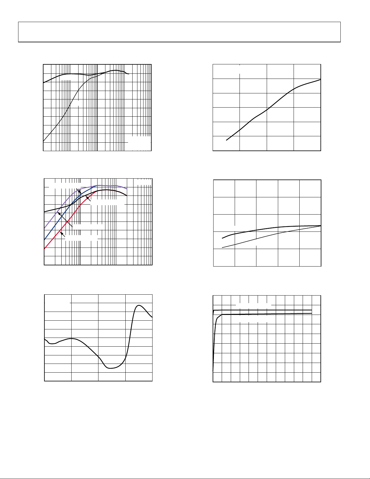
100
90
80
70
60
50
40
EFFICIENCY (%)
30
20
10
0
0.01 0.1 1 10
PSM
PWM
LOAD (A)
VIN = 12V
V
OUT
600kHz
Figure 5. Efficiency Plot of Figure 41, 10 A Output
100
V
= 1.8V PW M
OUT
90
80
V
= 1.05V PSM
70
60
50
40
EFFICIENCY (%)
30
20
10
0
0.01 0.1 1 10
V
OUT
= 1.05V PW M
V
V
= 1.05V_PWM
O
O
OUT
= 1.8V PSM
LOAD (A)
Figure 6. Efficiency Plot of Figure 44, 2 A Output
0.5
VIN = 12V
0.4
V
= 3.3V
OUT
0.3
0.2
0.1
0
–0.1
–0.2
LOAD REGULATION (%)
–0.3
–0.4
–0.5
0 5 10 15 20
LOAD (A)
Figure 7. Load Regulation of Figure 42
= 3.3V
VIN = 3V
100
08299-023
08299-024
08299-025
0.06
V
= 3.3V AT 1A L OAD
OUT
0.05
0.04
0.03
0.02
LINE REGULATION (%)
0.01
0
6 8 10 12 14
VIN (V)
Figure 8. Line Regulation of Figure 42
0
–0.05
–0.10
Δ VCCO (V)
–0.15
–0.20
–0.25
50mA LOAD
100mA LOAD
2.53.03.54.04.55.0
VIN (V)
Figure 9. LDO Load Regulation
5.10
5.05
5.00
4.95
4.90
4.85
VCCO (V)
4.80
4.75
4.70
4.65
5 7 9 11 13 15 17
NO LOAD ON LDO
100mA LOAD ON LDO
VIN (V)
Figure 10. LDO Line Regulation
08299-026
08299-027
08299-028
Rev. C | Page 10 of 32
Page 11

ADP1877
6
5
4
3
VCCO (V)
2
1
0
0123456
VIN (V)
Figure 11. VCCO vs. VIN
1
2
SW1
SW2
1
4
VIN = 3V
V
OUT
CH1 20mV
08299-029
1
2
VOUT1
OUTPUT RESPONSE
OUTPUT STEP LO AD 0.5A TO 0.8A
= 1.8V
CH4 500mA Ω
M100µs A CH4 750mA
Figure 14. Step Load Transient of Figure 44
DH1
DL1
08299-037
3
SYNC 600kHz
CH1 10V
CH3 5V
Figure 12. An Example of Synchronization, f
1
4
VIN = 12V
V
CH1 50mV
CH2 10V M1µs A CH1 5.60V
OUTPUT RESPONSE
5A TO 10A STE P LOAD
= 1.8V
OUT
CH4 5A Ω
M200µs A CH4 8.10A
SW
Figure 13. Step Load Transient of Figure 42, 5 A to 10 A
= 600 kHz
3
4
VIN = 12V
V
= 1.8V
OUT
OUTPUT PRECHARGED TO 1V
08299-035
CH3 1V
IL1
CH2 5VCH1 5V
CH4 1A Ω
M1ms A CH1 2.4V
08299-038
Figure 15. Soft Start into Precharged Output
EN IS TIED TO VIN
CSS = 100nF
1
2
4
3
08299-036
CH3 10V
VIN POWER SUPPLY
CH2 1VCH1 5V
CH4 500mV
V
(CH2)
OUT
SS
SW
M2ms A CH2 2.42V
08299-039
Figure 16. Power-On Sequence
Rev. C | Page 11 of 32
Page 12

ADP1877
1
3
2
4
1
2
3
SW
EN
CH3 1V
V
(CH3)
OUT
SS (CH4)
CH2 2VCH1 10V
CH4 1V
M10ms A CH2 1.52V
Figure 17. Enable Function
SW1
PGOOD1
VCCO (CH3)
V
, PRELOADE D (CH4)
OUT
CSS = 100nF
2.0
1.5
1.0
0.5
(%)
OSC
0
f
–0.5
–1.0
CHANGE IN
–1.5
–2.0
–2.5
08299-040
–40 –15 10 35 60 85 110 135
Figure 20. f
350
300
250
200
TIME (ns)
150
100
VIN = 12V; REFERENCED AT 25°C
TEMPERATURE (°C)
vs. Temperature
OSC
DH MINIMUM OFF TIM E
DH MINIMUM ON TIME
08299-031
4
CH3 2V
CH2 2VCH1 10V
CH4 2V Ω
M10ms A CH2 3.76V
Figure 18. Thermal Shutdown Waveform
0.5
0
–0.5
(%)
OSC
f
–1.0
–1.5
CHANGE IN
–2.0
–2.5
2468101214
Figure 19. Change in f
REFERENCE AT VIN = 2.75V
600kHz
300kHz
850kHz
VIN (V)
vs. VIN
OSC
50
08299-041
2.5 4.5 6.5 8.5 10.5 12.5 14.5
VIN (V)
08299-032
Figure 21. Typical DH Minimum On Time and Off Time
4
3
2
1
0
–1
–2
–3
CHANGE IN MINI M UM ON/OFF TIME (%)
–4
–40 –15 10 35 60 85 110 135
08299-030
DH MINIMUM OFF TIME
DH MINIMUM ON TIME
TEMPERATURE (°C)
08299-033
Figure 22. DH Minimum On Time and Off Time Overtemperature
Rev. C | Page 12 of 32
Page 13

ADP1877
THEORY OF OPERATION
The ADP1877 is a current mode (using ADI proprietary
Flex-Mode architecture), dual-channel, step-down switching
controller with integrated MOSFET drivers that drive N-channel
synchronous power MOSFETs. The two outputs are phase shifted
180°. This reduces the input RMS current, thus minimizing
required input capacitance.
The ADP1877 can be set to operate in pulse skip high efficiency
mode under light load or in forced PWM. The integrated boost
diodes in the ADP1877 reduce the overall system cost and
component count. The ADP1877 includes programmable soft
start, output overvoltage protection, programmable current
limit, power good, and tracking function. The ADP1877 can be
set to operate in any switching frequency between 200 kHz and
1.5 MHz with one external resistor.
CONTROL ARCHITECTURE
The ADP1877 is based on a fixed frequency current mode
PWM control architecture. The inductor current is sensed by
the voltage drop measured across the external low-side MOSFET
R
during the off period of the switching cycle (valley inductor
DSON
current). The current sense signal is further processed by the
current sense amplifier. The output of the current sense amplifier is
held, and the emulated current ramp is multiplexed and fed into
the PWM comparator as shown in Figure 23. The valley current
information is captured at the end of the off period, and the
emulated current ramp is applied at that point when the next on
cycle begins. An error amplifier integrates the error between the
feedback voltage and the generated the error voltage from the
COMP pin (from error amp in Figure 23).
TO
DRIVERS
FF
Q
I
RAMP
OSC Q
V
V
R
IN
RAMP
IN
S
R
benefits of using current mode control scheme still apply, such
as simplicity of loop compensation. Control logic enforces
antishoot-through operation to limit cross conduction of the
internal drivers and external MOSFETs.
OSCILLATOR FREQUENCY
The internal oscillator frequency, which ranges from 200 kHz to
1.5 MHz, is set by an external resistor, R
Some popular f
values are shown in Tab l e 4 , and a graphical
OSC
relationship is shown in Figure 24. For instance, a 78.7 kΩ
resistor sets the oscillator frequency to 800 kHz. Furthermore,
connecting FREQ to AGND or FREQ to VCCO sets the
oscillator frequency to 300 kHz or 600 kHz, respectively. For
other frequencies that are not listed in Tabl e 4 , the values of
R
FREQ
and f
can be obtained from Figure 24, or use the
OSC
following empirical formula to calculate these values:
−
×=Ω kHzfkR
)(96568)(
OSCFREQ
Table 4. Setting the Oscillator Frequency
R
f
FREQ
332 kΩ 200 kHz
78.7 kΩ 800 kHz
60.4 kΩ 1000 kHz
51 kΩ 1200 kHz
40.2 kΩ 1500 kHz
FREQ to AGND 300 kHz
FREQ to VCCO 600 kHz
410
360
310
R
FREQ
(kΩ) = 96568
, at the FREQ pin.
FREQ
065.1
(Typical)
OSC
f
OSC
(kHz)
–1.065
A
R
C
R
FROM
LOW SIDE
A
CS
MOSFET
08299-005
FROM
ERROR AMP
V
CS
Figure 23. Simplified Control Architecture
As shown in Figure 23, the emulated current ramp is generated
inside the IC but offers programmability through the RAMPx
pin. Selecting an appropriate value resistor from V
to the
IN
RAMP pin programs a desired slope compensation value and, at
the same time, provides a feed forward feature. The benefits
realized by deploying this type of control scheme are that there
is no need to worry about the turn-on current spike corrupting
the current ramp. Also, the current signal is stable because the
current signal is sampled at the end of the turn-off period,
which gives time for the switch node ringing to settle. Other
Rev. C | Page 13 of 32
260
(kΩ)
210
FREQ
R
160
110
60
10
100 400 700 1000 1300 1600 1900
f
(kHz)
OSC
Figure 24. R
FREQ
vs. f
OSC
08299-034
Page 14

ADP1877
MODE OF OPERATION
The SYNC pin is a multifunctional pin. PWM mode is enabled
when SYNC is connected to VCCO or a high logic. With SYNC
connected to ground or left floating, pulse skip mode is enabled.
Switching SYNC from low to high or high to low on the fly
causes the controller to transition from forced PWM to pulse
skip mode or pulse skip mode to forced PWM, respectively, in two
clock cycles.
1
2
3
DH1
DL1
OUTPUT
RIPPLE
Table 5. Mode of Operation Truth Table
SYNC Pin Mode of Operation
Low Pulse skip mode
High Forced PWM
No Connect Pulse skip mode
Clock Signal Forced PWM
The ADP1877 has a built-in pulse skip sensing circuitry that
allows the controller to skip PWM pulses, thus reducing the
switching frequency at light loads and, therefore, maintaining
high efficiency during a light load operation. The switching
frequency is a fraction of the natural oscillator frequency and is
automatically adjusted to regulate the output voltage. The
resulting output ripple is larger than that of the fixed frequency
forced PWM. Figure 25 shows that the ADP1877 operates in
PSM under a light load of 10 mA. Pulse skip frequency under a
certain light load is dependent on the inductor input and output
voltages.
SW1
1
COMP1 (CH2)
3
4
2
CH3 20mV
Figure 25. Example of Pulse Skip Mode Under a Light 5 mA Load
VOUT RIPPLE
INDUCTOR
CURRENT
CH2 200mVCH1 10V
CH4 2A Ω
M200µs A CH1 7.8V
08299-042
When the output load is greater than the pulse skip threshold
current (when V
reaches the threshold of 0.9 V), the
COMP
ADP1877 exits the pulse skip mode operation and enters the
fixed frequency discontinuous conduction mode (DCM), as
shown in Figure 26. When the load increases further, the
ADP1877 enters CCM.
4
CH3 20mV
Figure 26. Example of Discontinuous Conduction Mode (DCM) Waveform
INDUCTOR CURRENT
CH2 5VCH1 10V
CH4 2A Ω
M1µs A CH1 13.4V
08299-043
In forced PWM, the ADP1877 always operates in CCM at any
load. The inductor current is always continuous (and even goes
negative when there is no load); thus, efficiency is poor at light
loads.
SYNCHRONIZATION
The switching frequency of the ADP1877 can be synchronized
to an external clock by connecting SYNC to a clock signal,
which should be between 1× and 2.3× of the internal oscillator
frequency, f
. The resulting switching frequency, fSW, is ½ of
OSC
the external SYNC frequency because the SYNC input is
divided by 2, and the resulting phases are used to clock the two
channels alternately. In synchronization, the ADP1877 operates
in PWM, and f
equals ½ of f
SW
SYNC
.
When an external clock is detected at the first SYNC edge, the
internal oscillator is reset, and the clock control shifts to SYNC.
The SYNC edges then trigger subsequent clocking of the PWM
outputs. The DH1/DH2 rising edges appear approximately 100 ns
after the corresponding SYNC edge, and the frequency is locked
to the external signal. Depending on the start-up conditions of
Channel 1 and Channel 2, either Channel 1 or Channel 2 can be
the first channel synchronized to the rising edge of the SYNC
clock. If the external SYNC signal disappears during operation,
the ADP1877 reverts to its internal oscillator. When the SYNC
function is used, it is recommended to connect a pull-up
resistor from SYNC to VCCO so that when the SYNC signal is
lost, the ADP1877 continues to operate in PWM.
SOFT START
The soft start period is set by an external capacitor between
SS1/SS2 and AGND. When EN1/EN2 is enabled, a current source
of 6.5 µA starts charging the capacitor, and the regulation voltage is
reached when the voltage at SS1/SS2 reaches 0.6 V. For more
information, see the Applications Information section.
Rev. C | Page 14 of 32
Page 15

ADP1877
SYNCHRONOUS RECTIFIER AND DEAD TIME
The synchronous rectifier (low-side MOSFET) improves efficiency
by replacing the Schottky diode that is normally used in an
asynchronous buck regulator. In the ADP1877, the antishootthrough circuit monitors the SW and DL nodes and adjusts the
low-side and high-side drivers to ensure break-before-make
switching to prevent cross-conduction or shoot-through between
the high-side and low-side MOSFETs. This break-before-make
switching is known as the dead time, which is not fixed and
depends on how fast the MOSFETs are turned on and off. In a
typical application circuit that uses medium sized MOSFETs
with input capacitance of approximately 3 nF, the typical dead
time is approximately 30 ns. When small and fast MOSFETs are
used, the dead time can be as low as 13 ns.
INPUT UNDERVOLTAGE LOCKOUT
When the bias input voltage, VIN, is less than the undervoltage
lockout (UVLO) threshold, the switch drivers stay inactive.
When V
exceeds the UVLO threshold, the switchers start
IN
switching.
INTERNAL LINEAR REGULATOR
The internal linear regulator is low dropout (LDO), meaning it
can regulate its output voltage, VCCO. VCCO powers up the
internal control circuitry and provides power for the gate
drivers. It is guaranteed to have more than 200 mA of output
current capability, which is sufficient to handle the gate drive
requirements of typical logic threshold MOSFETs driven at up
to 1.5 MHz. VCCO is always active and cannot be shut down by
the EN1/EN2 pins. Bypass VCCO to AGND with a 1 µF or
greater capacitor.
Because the LDO supplies the gate drive current, the output of
VCCO is subject to sharp transient currents as the drivers
switch and the boost capacitors recharge during each switching
cycle. The LDO has been optimized to handle these transients
without overload faults. Due to the gate drive loading, using the
VCCO output for other external auxiliary system load is not
recommended.
The LDO includes a current limit well above the expected
maximum gate drive load. This current limit also includes a
short-circuit fold back to further limit the VCCO current in the
event of a short-circuit fault.
The VDL pin provides power to the low-side driver. Connect
VDL to VCCO. Bypass VDL to PGND with a 1 µF (minimum)
ceramic capacitor, which must be placed close to the VDL pin.
For an input voltage less than 5.5 V, it is recommended to
bypass the LDO by connecting VIN to VCCO, as shown in
Figure 27, thus eliminating the dropout voltage. However, for
example, if the input range is 4 V to 7 V, the LDO cannot be
bypassed by shorting VIN to VCCO because the 7 V input has
exceeded the maximum voltage rating of the VCCO pin. In this
case, use the LDO to drive the internal drivers, but keep in
mind that there is a dropout when V
is less than 5 V.
IN
VIN= 2.75V TO 5.5V
VIN VCCO
ADP1877
08299-006
Figure 27. Configuration for V
< 5.5 V
IN
OVERVOLTAGE PROTECTION
The ADP1877 has a built-in circuit for detecting output
overvoltage at the FB node. When the FB voltage, V
, rises
FB
above the overvoltage threshold, the low-side NMOSFET is
immediately turned on, and the high-side NMOSFET is turned
off until the V
drops below the undervoltage threshold. This
FB
action is known as the crowbar overvoltage protection. If the
overvoltage condition is not removed, the controller maintains
the feedback voltage between the overvoltage and undervoltage
thresholds, and the output is regulated to within approximately
+16% and −10% of the regulation voltage. During an overvoltage
event, the SS node discharges toward zero through an internal
1 kΩ pull-down resistor. When the voltage at FB drops below
the undervoltage threshold, the soft start sequence restarts. The
following graph shows the overvoltage protection scheme in
action in PSM.
1
2
3
4
CH3 5V
Figure 28. Overvoltage Protection in PSM
DH1
PGOOD1
VO1 = 1.8V S H ORTED
TO 2.2V SOURCE
CH2 5VCH1 10V
CH4 500mV
VIN (CH3)
M200µs
A CH4 2.05V
08299-044
POWER GOOD
The PGOODx pin is an open-drain NMOS with an internal 12 kΩ
pull-up resistor connected between PGOODx and VCCO.
PGOODx is internally pulled up to VCCO during normal
operation and is active low when tripped. When the feedback
voltage, V
below the undervoltage threshold, the PGOODx output is
pulled to ground after a delay of 12 µs. The overvoltage or
undervoltage condition must exist for more than 12 µs for
PGOODx to become active. The PGOODx output also becomes
active if a thermal overload condition is detected.
, rises above the overvoltage threshold or drops
FB
Rev. C | Page 15 of 32
Page 16

ADP1877
SHORT CIRCUIT AND CURRENT LIMIT PROTECTION
When the output is shorted or the output current exceeds the
current limit set by the R
the ADP1877 shuts off both the high-side and low-side drivers
and restarts the soft start sequence every 10 ms, which is known
as hiccup mode. The SS node discharges to zero through an
internal 1 kΩ resistor during an overcurrent or short-circuit
event. Figure 29 shows that the ADP1877 (a 20 A application
circuit) is entering current limit hiccup mode when the output
is shorted.
1
3
4
CH1 10V
CH3 500mV
Figure 29. Current Limit Hiccup Mode, 20 A Circuit
INDUCTOR CURRENT
CH4 10A Ω
resistor for eight consecutive cycles,
ILIM
SW1
SS1
M2ms A CH1 11.2V
08299-045
SHUTDOWN CONTROL
The EN1 and EN2 pins are used to enable or disable Channel 1
and Channel 2, respectively, of the ADP1877. The precision enable
threshold for EN1/EN2 is typically 0.63 V. When the EN1/EN2
voltage rises above 0.63 V, the ADP1877 is enabled and starts
normal operation after the soft start period. When the voltage
at EN1/EN2 drops below 0.57 V, the switchers and the internal
circuits in the ADP1877 are turned off. Note that EN1/EN2
cannot shut down the LDO at VCCO, which is always active.
For the purpose of start-up power sequencing, the startup of the
ADP1877 can be programmed by connecting an appropriate
resistor divider from the master power supply to the EN1/EN2
pin, as shown in Figure 30. For instance, if the desired start-up
voltage from the master power supply is 10 V, R1 and R2 can be
set to 156 kΩ and 10 kΩ, respectively.
MASTER
SUPPLY
VOLTAGE
ADP1877
R1
EN1
FB1
OR
EN2
R2
Figure 30. Optional Power-Up Sequencing Circuit
FB2
OR
V
OUT1
R
TOP
R
BOT
08299-007
THERMAL OVERLOAD PROTECTION
The ADP1877 has an internal temperature sensor that senses
the junction temperature of the chip. When the junction
temperature of the ADP1877 reaches approximately 155°C, the
ADP1877 goes into thermal shutdown, the converter is turned
off, and SS discharges toward zero through an internal 1 kΩ
resistor. At the same time, VCCO discharges to zero. When the
junction temperature drops below 135°C, the ADP1877 resumes
normal operation after the soft start sequence.
Rev. C | Page 16 of 32
Page 17

ADP1877
APPLICATIONS INFORMATION
SETTING THE OUTPUT VOLTAGE
The output voltage is set using a resistive voltage divider from
the output to FB. The voltage divider divides down the output
voltage to the 0.6 V FB regulation voltage to set the regulation
output voltage. The output voltage can be set to as low as 0.6 V
and as high as 90% of the power input voltage.
The maximum input bias current into FB is 100 nA. For a 0.15%
degradation in regulation voltage and with 100 nA bias current,
the low-side resistor, R
in 67 µA of divider current. For R
, must be less than 9 kΩ, which results
BOT
, use a 1 k to 20 k resistor.
BOT
A larger value resistor can be used but results in a reduction in
output voltage accuracy due to the input bias current at the FB
pin, while lower values cause increased quiescent current
consumption. Choose R
to set the output voltage by using
TOP
the following equation:
⎛
OUT
⎜
RR
=
BOTTOP
⎜
V
⎝
⎞
VV
−
FB
⎟
⎟
FB
⎠
where:
R
is the high-side voltage divider resistance.
TOP
is the low-side voltage divider resistance.
R
BOT
V
is the regulated output voltage.
OUT
is the feedback regulation threshold, 0.6 V.
V
FB
The minimum output voltage is dependent on f
DH on time. The maximum output voltage is dependent on f
and minimum
SW
SW
the minimum DH off time, and the IR drop across the high-side
N-channel MOSFET (NMOSFET) and the DCR of the inductor.
For example, with an f
of 600 kHz (or 1.67 µs) and minimum on
SW
time of 130 ns, the minimum duty cycle is approximately 7.8%
(130 ns/1.67 µs). If V
is 12 V and the duty cycle is 7.8%, then
IN
the lowest output is 0.94 V. As an example for the maximum output
voltage, if V
is 5 V, fSW is 600 kHz, and the minimum DH off
IN
time is 390 ns (330 ns DH off time plus approximately 60 ns
total dead time), then the maximum duty cycle is 76%. Therefore,
the maximum output is approximately 3.8 V. If the IR drop
across the high-side NMOSFET and the DCR of the inductor is
0.5 V, then the absolute maximum output is 4.5 V (5 V − 0.5 V),
independent of f
and duty cycle.
SW
SOFT START
Program the soft start by connecting a capacitor from SSx to
AGND. The soft start function limits the input inrush current
and prevents the output overshoot.
On startup, a 6.5 µA current source charges the SSx capacitor.
The soft start period is approximated by
V
tμ=
6.0
5.6
C
SSSS
A
,
Once the voltage at SSx exceeds the regulation voltage (typically
0.6 V), the reverse current is reenabled to allow the output
voltage regulation to be independent of load current.
When a controller is disabled, for instance, EN1/EN2 is pulled
low or experiences an overcurrent limit condition, the soft start
capacitor is discharged through an internal 1 kΩ pull-down
resistor.
SETTING THE CURRENT LIMIT
The current limit comparator measures the voltage across the
low-side MOSFET to determine the load current.
The current limit is set by an external current limit resistor,
. The current sense pin, ILIMx, sources 50 A to this external
R
ILIM
resistor. This creates an offset voltage of R
50 A. When the drop across the low-side MOSFET, R
multiplied by
ILIM
DSON
, is
equal to or greater than this offset voltage, the ADP1877 flags a
current limit event.
Because the ILIMx current and the MOSFET, R
, vary over
DSON
process and temperature, the minimum current limit should be
set to ensure that the system can handle the maximum desired
load current. To do this, use the peak current in the inductor,
which is the desired output current limit level plus ½ of the
ripple current, the maximum R
of the MOSFET at its
DSON
highest expected temperature, and the minimum ILIM current.
ILIM
LPK
=
R
40
MAXDSON
_
A
μ
RI
×
where:
I
is the peak inductor current.
LPK
The buck converters usually run a fairly high current. PCB
layout and component placement may affect the current limit
setting. An iteration of the R
value may be required for a
ILIM
particular board layout and MOSFET selection. If alternative
MOSFETs are substituted at some point in production, these
resistor values may also need an iteration. Keep in mind that the
temperature coefficient of the MOSFET, R
o
0.4%/
C.
, is typically
DSON
ACCURATE CURRENT LIMIT SENSING
R
of the MOSFET can vary by more than 50% over the
DSON
temperature range. Accurate current limit sensing can be
achieved by adding a current sense resistor from the source of
the low-side MOSFET to PGND. Make sure that the power
rating of the current sense resistor is adequate for the application.
Apply the above equation and calculate R
R
DSON_MAX
with R
. The Figure 31 illustrates the
SENSE
implementation of this accurate current limit sensing.
by replacing
ILIM
The SSx pin reaches a final voltage equal to VCCO. If the output
voltage is precharged prior to turn-on, the ADP1877 prevents
reverse inductor current, which discharges the output capacitor.
Rev. C | Page 17 of 32
Page 18

ADP1877
ADP1877
DHx
SWx
ILIMx
DLx
Figure 31. Accurate Current Limit Sensing
R
ILIM
VIN
R
SENSE
08299-008
SETTING THE SLOPE COMPENSATION
In a current-mode control topology, slope compensation is
needed to prevent subharmonic oscillations in the inductor
current and to maintain a stable output. The external slope
compensation is implemented by summing the amplified sense
signal and a scaled voltage at the RAMPx pin. To implement the
slope compensation, connect a resistor between RAMPx and
the input voltage. The resistor, R
10
106.3××
=
R
RAMP
L
RA
MAXDSONCS
_
where:
10
3.6 × 10
is an internal parameter.
L is the inductance of the inductor.
R
A
is the the low-side MOSFET maximum on resistance.
DSON_MAX
is the gain, either 3 V/V, 6 V/V, 12 V/V, or 24 V/V, of the
CS
current sense amplifier (see the Setting the Current Sense Gain
section for more details).
Keep in mind that R
as much as 0.4%/
is temperature dependent and can vary
DSON
o
C. Choose R
temperature. The voltage at RAMPx is fixed at 0.2 V, and the
current going into RAMPx should be in between 6 µA and
200 µA. Make sure that the following condition is satisfied:
V
A6 ≤
≤
V2.0
−
IN
R
RAMP
For instance, with an input voltage of 12 V, R
exceed 1.9 MΩ. If the calculated R
then select a R
value that produces between 6 µA and 20 µA.
RAMP
Figure 32 illustrates the connection of the slope compensation
resistor R
and the current sense gain resistor R
RAMP
, is calculated by
RAMP
at the maximum operating
DSON
A200
should not
RAMP
produces less than 6 µA,
RAMP
CSG
VIN
.
SETTING THE CURRENT SENSE GAIN
The voltage drop across the external low-side MOSFET is
sensed by a current sense amplifier by multiplying the peak
inductor current and the R
then amplified by a gain factor of either 3 V/V, 6 V/V, 12 V/V,
or 24 V/V, which is programmable by an external resistor, R
connected to the DL pin. This gain is sensed only during
power-up and not during normal operation. The amplified
voltage is summed with the slope compensation ramp voltage
and fed into the PWM controller for a stable regulation voltage.
The voltage range of the internal node, V
and 2.2 V. Select the current sense gain such that the internal
minimum amplified voltage (V
maximum amplified voltage (V
above 2.1 V to account for temperature and part-to-part
variations. Note that V
CSMIN
which has a range of 0.75 V to 2.25 V. The following are
equations for V
CSMIN
CSMIN
75.0
and V
where:
is the minimum amplified voltage of the internal current
V
CSMIN
sense amplifier at zero output current.
V
is the maximum amplified voltage of the internal current
CSMAX
sense amplifier at maximum output current.
R
is the the low-side MOSFET minimum on resistance.
DSON_MIN
The zero-current level voltage of the current sense amplifier is
0.75 V.
is the peak-to-peak ripple current in the inductor.
I
LPP
is the maximum output DC load current.
I
LOADMAX
Tabl e 6 shows the appropriate current sense gain settings for a
given R
maximum load current and a 33% inductor current
DSON
ripple. Because of the variation in R
(part-to-part variation and overtemperature) and the variation
of the inductors, the users must verify that V
exceed 2.2 V at the maximum output load current.
of the MOSFET. The result is
DSON
, is between 0.4 V
CS
) is above 0.4 V and the
CSMIN
) is 2.1 V. Do not set V
CSMAX
or V
CSMAX
is not the same as V
CSMAX
:
1
LPP
2
(75.0
LOADMAXCSMAX
_
1
)
LPP
2
of the power MOSFETs
DSON
ARIVV ××−=
COMP
CSMINDSON
_
does not
CSG
CSMAX
COMP
ARIIVV ××++=
,
,
CSMAXDSON
R
RAMP
RAMP
DHx
SWx
ILIMx
DLx
ADP1877
Figure 32. Slope Compensation and CS Gain Connection
R
ILIM
R
CSG
08299-009
Rev. C | Page 18 of 32
Page 19

ADP1877
Table 6. CS Gain Setting Selection Table for Some Popular Configurations
I
= 33% Load ACS = 3 ACS = 6 ACS = 12 ACS = 24
LPP
R
(mΩ) Load (A) VCS Min (V) VCS Max (V) VCS Min (V) VCS Max (V) VCS Min (V) VCS Max (V) VCS Min (V) VCS Max (V)
DSON
1.5 25 0.73 0.9 0.71 1.01 0.7 1.3 0.6 1.80
2 25 0.73 0.9 0.70 1.10 0.7 1.4
2 20 0.73 0.9 0.71 1.03 0.7 1.3
3 20 0.72 1.0 0.69 1.17 0.6 1.6
5 15 0.71 1.0 0.68 1.27 0.6 1.8
7 10 0.72 1.0 0.68 1.24 0.6 1.7
10 10 0.70 1.1 0.65 1.45
15 8 0.69 1.2 0.63 1.59
18 8 0.68 1.3 0.61 1.76
20 7 0.68 1.2 0.61 1.73
25 5 0.69 1.2 0.63 1.62
30 5 0.68 1.3 0.60 1.80
40 5 0.65 1.4
60 3 0.66 1.4
80 2 0.67 1.3
100 2 0.65 1.4
120 2 0.63 1.6
INPUT CAPACITOR SELECTION
The input current to a buck converter is a pulse waveform. It is
zero when the high-side switch is off and approximately equal
to the load current when it is on. The input capacitor carries the
input ripple current, allowing the input power source to supply
only the direct current. The input capacitor needs sufficient
ripple current rating to handle the input ripple, as well as an
ESR that is low enough to mitigate input voltage ripple. For the
usual current ranges for these converters, it is good practice to
use two parallel capacitors placed close to the drains of the
high-side switch MOSFETs (one bulk capacitor of sufficiently
high current rating and a 10 F ceramic decoupling capacitor,
typically).
Select an input bulk capacitor based on its ripple current rating.
First, determine the duty cycle of the output.
V
OUT
D =
The input capacitor RMS ripple current is given by
where:
I
is the output current.
O
D is the duty cycle
The minimum input capacitance required for a particular load is
C
V
IN
)1( DDII
−=
ORMS
−×
DDI
=
MININ
,
O
PP
)1(
fDRIV
×−
)(
SWESRO
where:
is the desired input ripple voltage.
V
PP
R
is the equivalent series resistance of the capacitor.
ESR
If an MLCC capacitor is used, the ESR is near 0, then the
equation is simplified to
DD
−×=)1(
IC
,
MININ
O
PP
fV
×
SW
The capacitance of MLCC is voltage dependent. The actual
capacitance of the selected capacitor must be derated accordingly.
In addition, add more bulk capacitance, such as by using
electrolytic or polymer capacitors, as necessary for large step
load transisents. Make sure the current ripple rating of the bulk
capacitor exceeds the minimum input current ripple of a
particular design.
INPUT FILTER
Normally the input pin, VIN, with a 0.1 µF or greater value
bypass capacitor to AGND, is sufficient for filtering out any
unwanted switching noise. However, depending on the PCB
layout, some switching noises can be passed down to the ADP1877
internal circuitry; therefore, it is recommended to have a low
pass filter at the VIN pin. Connecting a resistor, between 2 Ω
and 5 Ω, in series with VIN and a 1 µF ceramic capacitor
between VIN and AGND creates a low pass filter that effectively
filters out any unwanted glitches caused by the switching
regulator. Keep in mind that the input current could be larger than
100 mA when driving large MOSFETs. A 100 mA across a 5 Ω
resistor creates a 0.5 V drop, which is the same voltage drop in
VCCO. In this case, a lower resistor value is desirable.
Rev. C | Page 19 of 32
Page 20

ADP1877
2Ω TO 5Ω
VIN
1µF
Figure 33. Input Filter Configuration
VIN
ADP1877
AGND
08299-010
BOOST CAPACITOR SELECTION
To lower system component count and cost, the ADP1877 has a
built-in rectifier (equivalent to the boost diode) between VCCO
and BSTx. Choose a boost ceramic capacitor with values
between 0.1 µF and 0.22 µF, which provides the current for the
high-side driver during switching.
INDUCTOR SELECTION
The output LC filter smoothes the switched voltage at SWx.
Choose an inductor value such that the inductor ripple current
is approximately 1⁄3 of the maximum dc output load current.
Using a larger value inductor results in a physical size larger
than required, and using a smaller value results in increased
losses in the inductor and/or MOSFET switches and larger
voltage ripples at the output.
Choose the inductor value by the following equation:
IN
L ×
=
SW
Δ×
OUT
OUT
V
If
IN
L
V
VV
−
where:
L is the inductor value.
f
is the switching frequency.
SW
is the output voltage.
V
OUT
V
is the input voltage.
IN
ΔI
is the inductor ripple current, typically 1⁄3 of the maximum
L
dc load current.
OUTPUT CAPACITOR SELECTION
Choose the output bulk capacitor to set the desired output voltage
ripple. The impedance of the output capacitor at the switching
frequency multiplied by the ripple current gives the output
voltage ripple. The impedance is made up of the capacitive
impedance plus the nonideal parasitic characteristics, the
equivalent series resistance (ESR), and the equivalent series
inductance (ESL). The output voltage ripple can be
approximated with
OUT
⎛
⎜
+Δ≅Δ
RIV 4
L
ESR
⎜
⎝
1
×
Cf
8
SW
OUT
where:
ΔV
is the output ripple voltage.
OUT
ΔI
is the inductor ripple current.
L
R
is the equivalent series resistance of the output capacitor (or
ESR
the parallel combination of ESR of all output capacitors).
is the equivalent series inductance of the output capacitor
L
ESL
(or the parallel combination of ESL of all capacitors).
⎞
⎟
×+
Lf
ESLSW
⎟
⎠
Solving C
Usually, the impedance is dominated by ESR, such as in
electrolytic or polymer capacitors, at the switching frequency, as
stated in the maximum ESR rating on the capacitor data sheet;
therefore, output ripple reduces to
Electrolytic capacitors also have significant ESL, on the order of
5 nH to 20 nH, depending on type, size, and geometry. PCB
traces contribute some ESR and ESL, as well. However, using
the maximum ESR rating from the capacitor data sheet usually
provides some margin such that measuring the ESL is not
usually required.
In the case of output capacitors where the impedance of the ESR
and ESL are small at the switching frequency, for instance,
where the output cap is a bank of parallel MLCC capacitors, the
capacitive impedance dominates and the output capacitance
equation reduces to
Make sure that the ripple current rating of the output capacitors
is greater than the maximum inductor ripple current.
During a load step transient on the output, for instance, when
the load is suddenly increased, the output capacitor supplies the
load until the control loop has a chance to ramp the inductor
current. This initial output voltage deviation results in a voltage
droop or undershoot. The output capacitance, assuming 0 ESR,
required to satisfy the voltage droop requirement can be
approximated by
where:
∆I
STEP
∆V
DROOP
When a load is suddenly removed from the output, the energy
stored in the inductor rushes into the capacitor, causing the
output to overshoot. The output capacitance required to satisfy
the output overshoot requirement can be approximated by
where:
∆V
OVERSH OOT
Select the largest output capacitance given by any of the
previous three equations.
in the previous equation yields
OUT
I
Δ
OUT
L
×
≅
8
SW
≅
8
≅
OUT
RIV ×Δ≅Δ
L
ESR
I
Δ
L
fV
×Δ
SW
OUT
Δ
I
STEP
fV
×Δ
SWDROOP
C
OUT
C
OUT
C
OUT
1
4
L
ESR
is the step load.
is the voltage droop at the output.
2
LI
Δ
C
≅
OUT
STEP
2
)(
VVV
−Δ+
OUTOVERSHOOTOUT
is the overshoot voltage during the step load.
LfIRIVf
×Δ−Δ−Δ
L
2
ESLSW
Rev. C | Page 20 of 32
Page 21

ADP1877
MOSFET SELECTION
The choice of MOSFET directly affects the dc-to-dc converter
performance. A MOSFET with low on resistance reduces I
losses, and low gate charge reduces transition losses. The
MOSFET should have low thermal resistance to ensure that the
power dissipated in the MOSFET does not result in excessive
MOSFET die temperature.
The high-side MOSFET carries the load current during on time
and usually carries most of the transition losses of the converter.
Typically, the lower the on resistance of the MOSFET, the
higher the gate charge and vice versa. Therefore, it is important
to choose a high-side MOSFET that balances the two losses. The
conduction loss of the high-side MOSFET is determined by the
equation
⎞
⎛
2
×≅
)(
V
OUT
⎟
⎜
RIP
DSONLOADC
⎜
⎝
⎟
V
IN
⎠
where:
R
is the MOSFET on resistance.
DSON
The gate charging loss is approximated by the equation
PV
G
fQVP ××≅
SWG
where
is the gate driver supply voltage.
V
PV
is the MOSFET total gate charge.
Q
G
Note that the gate charging power loss is not dissipated in the
MOSFET but rather in the ADP1877 internal drivers. This
power loss should be taken into consideration when calculating
the overall power efficiency.
The high-side MOSFET transition loss is approximated by the
equation
fttIV
×+××
)(
IN
≅
P
T
LOAD
FR
SW
2
where:
P
is the high-side MOSFET switching loss power.
T
is the rise time in charging the high-side MOSFET.
t
R
t
is the fall time in discharging the high-side MOSFET.
F
t
and tF can be estimated by
R
Q
GSW
GSW
RISEDRIVER
_
FALLDRIVER
_
t
≅
R
I
Q
t
≅
F
I
where:
Q
is the gate charge of the MOSFET during switching and is
GSW
given in the MOSFET data sheet.
I
DRIVER_RISE
and I
DRIVER_FALL
are the driver current put out by the
ADP1877 internal gate drivers.
is not given in the data sheet, it can be approximated by
If Q
GSW
Q
GS
QQ +≅
GDGSW
2
2
R
Rev. C | Page 21 of 32
where:
Q
and QGS are the gate-to-drain and gate-to-source charges
GD
given in the MOSFET data sheet.
I
DRIVER_RISE
I
I
and I
_
FALLDRIVER
_
DRIVER_FALL
RISEDRIVER
can be estimated by
≅
≅
DD
SOURCEON
_
V
SP
+
SINKON
_
VV
−
SP
RR
+
GATE
RR
GATE
where:
V
is the input supply voltage to the driver and is between 2.75 V
DD
and 5 V, depending on the input voltage.
V
is the switching point where the MOSFET fully conducts;
SP
this voltage can be estimated by inspecting the gate charge
graph given in the MOSFET data sheet.
R
ON_SOURCE
is the on resistance of theADP1877 internal driver,
given in Tab le 1 , when charging the MOSFET.
R
is the on resistance of the ADP1877 internal driver,
ON_SINK
given in Tab le 1 , when discharging the MOSFET.
R
is the on gate resistance of MOSFET given in the
GATE
MOSFET data sheet. If an external gate resistor is added, add
this external resistance to R
GATE
.
The total power dissipation of the high-side MOSFET is the
sum of conduction and transition losses:
PPP +≅
CHS
T
The synchronous rectifier, or low-side MOSFET, carries the
inductor current when the high-side MOSFET is off. The lowside MOSFET transition loss is small and can be neglected in
the calculation. For high input voltage and low output voltage,
the low-side MOSFET carries the current most of the time.
Therefore, to achieve high efficiency, it is critical to optimize
the low-side MOSFET for low on resistance. In cases where the
power loss exceeds the MOSFET rating or lower resistance is
required than is available in a single MOSFET, connect multiple
low-side MOSFETs in parallel. The equation for low-side
MOSFET conduction power loss is
2
⎡
RIP 1)(
−×≅
⎢
DSONLOADCLS
⎣
⎤
V
OUT
⎥
V
IN
⎦
There is also additional power loss during the time, known as
dead time, between the turn-off of the high-side switch and the
turn-on of the low-side switch, when the body diode of the lowside MOSFET conducts the output current. The power loss in
the body diode is given by
IftVP ×××=
BODYDIODE
DF
OSW
where:
V
is the forward voltage drop of the body diode, typically 0.7 V.
F
t
is the dead time in the ADP1877, typically 30 ns when
D
driving some medium-size MOSFETs with input capacitance of
approximately 3 nF.
Page 22

ADP1877
Then the power loss in the low-side MOSFET is
PPP +=
BODYDIODECLSLS
Note that MOSFET, R
temperature with a typical temperature coefficient of 0.4%/
, increases with increasing
DSON
o
C.
The MOSFET junction temperature rise over the ambient
temperature is
T
= TA + θ
J
JA
× P
D
where:
θ
is the thermal resistance of the MOSFET package.
JA
T
is the ambient temperature.
A
P
is the total power dissipated in the MOSFET.
D
LOOP COMPENSATION
As with most current mode step-down controller, a transconductance error amplifier is used to stabilize the external voltage
loop. Compensating the ADP1877 is fairly easy; an RC
compensator is needed between COMP and AGND. Figure 34
shows the configuration of the compensation components:
, C
R
COMP
C
COMP
compensation analysis.
The open loop gain transfer function at angular frequency, s, is
given by
where:
G
is the transconductance of the error amplifer, 500 µs.
m
G
is the tranconductance of the current sense amplifier.
CS
Z
COMP
Z
FILTER
V
= 0.6 V
REF
G
with units of A/V is given by
CS
where:
A
is the current sense gain of either 3 V/V, 6 V/V, 12 V/V, or
CS
24 V/V set by the gain resistor between DL and PGND.
R
DSON_MIN
, and CC2. Because CC2 is very small compared to
COMP
, to simplify calculation, CC2 is ignored for the stability
COMPx
R
COMP
C
C2
C
COMP
Figure 34. Compensation Components
V
GGsH
m
REF
CS
V
OUT
0.6V
AGND
ADP1877
COMP
FBx
G
m
08299-011
FILTER
)()()( sZsZ
(1)
××××=
is the impedance of the compensation network.
is the impedance of the output filter.
G
=
CS
1
RA
×
(2)
MINDSONCS
_
is the the low-side MOSFET minimum on resistance.
Because the zero produced by the ESR of the output capacitor is
not needed to stabilize the control loop, the ESR is ignored for
analysis. Then Z
Z
=
FILTER
Because C
is very small relative to C
C2
is given by
FILTER
1
(3)
sC
OUT
, Z
COMP
1
RZ
COMPCOMP
1
+=
sC
=
COMP
can be written as
COMP
CsR
×+
sC
COMP
COMPCOMP
(4)
At the crossover frequency, the open loop transfer function is
unity of 0 dB, H (f
Equation 3, Z
COMP
fZ
CROSSCOMP
The zero produced by R
f×π=
ZERO
2
) = 1. Combining Equation 1 and
CROSS
at the crossover frequency can be written as
is
VC
×
OUTOUT
))(
V
REF
(5)
=
1
m
COMP
CR
GG
×
CS
and C
COMP
(6)
COMPCOMP
f
×
π
2
CROSS
()(
At the crossover frequency, Equation 4 can be shown as
ff
+
RfZ
COMPCROSSCOMP
CROSS
×=)(
Combining Equations 5 and Equation 7 and solving for R
f
CROSS
ZERO
(7)
COMP
gives
R
COMP
f
×π
ZERO
2
CROSS
×
(
m
×
GG
×
CS
f
CROSS
=
CROSS
ff
+
VC
×
OUTOUT
(8)
)()
V
REF
Choose the crossover and zero frequencies as follows:
f
f =
CROSS
f ==
ZERO
SW
(9)
13
ff
SWCROSS
(10)
655
Substituting Equation 2, Equation 9, and Equation 10 into
Equation 8 yields
f
×π
2
RAR
=
××
DSONCSCOMP
CROSS
(83.0
×
G
m
VC
×
OUTOUT
(11)
)()
V
REF
where:
G
is the transconductance of the error amplifer, 500 µs.
m
A
is the current sense gain of 3 V/V, 6 V/V, 12 V/V or 24 V/V.
CS
R
is on resistance of the low-side MOSFET.
DSON
V
= 0.6 V
REF
And combining Equation 6 and Equation 10 yields
C
=
COMP
And lastly set C
1
20
2
×π
to
C2
2
(12)
fR
CROSSCOMP
1
10
(13)
CCC ×≤≤×
COMPCCOMP
Rev. C | Page 22 of 32
Page 23

ADP1877
SWITCHING NOISE AND OVERSHOOT REDUCTION
In any high speed step-down regulator, high frequency noise
(generally in the range of 50 MHz to 100 MHz) and voltage
overshoot are always present at the gate, the switch node (SW),
and the drains of the external MOSFETs. The high frequency
noise and overshoot are caused by the parasitic capacitance,
, of the external MOSFET and the parasitic inductance of
C
GD
the gate trace and the packages of the MOSFETs. When the high
current is switched, electromagnetic interference (EMI) is
generated, which can affect the operation of the surrounding
circuits. To reduce voltage ringing and noise, it is required to
add an RC snubber between SW and PGND for applications with
more than 10 A output current, as illustrated in Figure 35.
Snubbers may also be needed in applications where the duty
cycle in one of the channels is higher than or equal to 50%.
In most applications, R
is typically 2 Ω to 4 Ω, and C
SNUB
typically 1.2 nF to 3 nF.
R
can be estimated by
SNUB
L
MOSFET
R 2≅
SNUB
And C
where
L
MOSFET
can be estimated by
SNUB
CC ≅
OSSSNUB
:
is the total parasitic inductance of the high-side and
C
OSS
low-side MOSFETs, typically 3 nH, and is package dependent.
C
is the total output capacitance of the high-side and low-
OSS
side MOSFETs given in the MOSFET data sheet.
The size of the RC snubber components need to be chosen
correctly to handle the power dissipation. The power dissipated
is
in R
SNUB
2
SNUB
IN
In most applications, a component size 0805 for R
fCVP ××=
SWSNUB
is sufficient.
SNUB
However, the use of an RC snubber reduces the overall efficiency,
generally by an amount in the range of 0.1% to 0.5%. The RC
snubber cannot reduce the voltage overshoot. A resistor, shown
in Figure 35, at the BSTx pin helps to reduce overshoot
as R
RISE
and is generally between 2 Ω and 4 Ω. Adding a resistor in
series, typically between 2 Ω and 4 Ω, with the gate driver also
helps to reduce overshoot. If a gate resistor is added, then R
is not needed.
VDL
PGND1
ADP1877
(CHANNEL 1)
BST1
DH1
SW1
ILIM1
DL1
R
RISE
Figure 35. Application Circuit with a Snubber
VIN
M1
L
R
ILIM1
M2
R
C
SNUB
SNUB
VOUT
COUTx
SNUB
RISE
08299-012
Rev. C | Page 23 of 32
VOLTAGE TRACKING
The ADP1877 includes a tracking feature that tracks a master
voltage. This feature is especially important when the ADP1877
is powering separate power supply voltages on a single integrated
circuit, such as the core and I/O voltages of a DSP or microcontroller. In these cases, improper sequencing can cause damage
to the load.
In all tracking configurations, the output can be set as low as 0.6 V
for a given operating condition. The soft start time setting of
the master voltage should be longer than the soft start of the
slave voltage. This forces the rise time of the master voltage to
be imposed on the slave voltage. If the soft start setting of the
slave voltage is longer, the slave comes up more slowly, and the
tracking relationship is not seen at the output.
Two tracking configurations are possible with the ADP1877:
coincident and ratiometric trackings. Full time DDR termination is
not recommended when using these tracking features.
COINCIDENT TRACKING
The most common application is coincident tracking, used in
core vs. I/O voltage sequencing and similar applications.
Coincident tracking limits the slave output voltage to be the
same as the master voltage until it reaches regulation. Connect
the slave TRK input to a resistor divider from the master voltage
that is the same as the divider used on the slave FB pin. This
forces the slave voltage to be the same as the master voltage. For
= R
coincident tracking, use R
in Figure 37.
VOLTAGE (V)
Figure 36. Coincident Tracking
EN
EN1 EN2
1MΩ
VCCO
C
100nF
SS1
TRK1
ADP1877
SS1
FB2
R
BOT
10kΩ
R
20kΩ
Figure 37. Example of a Coincident Tracking Circuit
TRKT
MASTER VOLTAGE
SLAVE VOLTAGE
TIME
FB1
TRK2
SS2
TOP
and R
TOP
C
20nF
1.8V
V
OUT2_SLAVE
45.3kΩ
10kΩ
SS2
TRKB
R
20kΩ
1.1V
R
10kΩ
= R
BOT
08299-013
3.3
V
V
OUT1_MASTER
TRKT
TRKB
, as shown
08299-014
Page 24

ADP1877
The ratio of the slave output voltage to the master voltage is a
function of the two dividers.
⎛
⎜
1
V
OUT
_
SLAVE
V
_
OUT
MASTER
⎜
⎝
=
⎛
⎜
+
1
⎜
⎝
⎞
R
TOP
⎟
+
⎟
R
BOT
⎠
⎞
R
TRKT
⎟
⎟
R
TRKB
⎠
As the master voltage rises, the slave voltage rises identically.
Eventually, the slave voltage reaches its regulation voltage,
where the internal reference takes over the regulation while the
TRKx input continues to increase and thus removes itself from
influencing the output voltage.
To ensure that the output voltage accuracy is not compromised
by the TRKx pin being too close in voltage to the 0.6 V
reference, make sure that the final value of the TRKx voltage of
the slave channel is at least 0.7 V.
RATIOMETRIC TRACKING
Ratiometric tracking limits the output voltage to a fraction of
the master voltage. For ratiometric tracking, the simplest
configuration is to tie the TRK pin of the slave channel to the
FBx pin of the master channel. However, because of the large
internal offset between TRKx and FBx, this ratiometric tracking
configuration is not recommended. A tracking configuration
that requires the TRKx voltage of the slave channel below 0.6 V
is not recommended because of the large internal TRKx to FBx
offset voltage.
Another ratiometric tracking configuration is having the slave
channel rise more quickly than the master channel, as shown in
Figure 38 and Figure 39. The tracking circuits in Figure 37 and
Figure 38 are virtually identical with the exception that RTRKB
> RTRKT, as shown in Figure 38.
3.3V
V
OUT1_MASTER
R
TRKT
5kΩ
2.2V
R
TRKB
10kΩ
VCCO
100nF
EN
1MΩ
EN1 EN2
FB1
TRK1
45.3kΩ
10kΩ
ADP1877
FB2
TRK2
SS2
C
SS2
20nF
C
SS1
SS1
R
BOT
10kΩ
R
TOP
20kΩ
1.8V
V
OUT2_SLAVE
Figure 38. A Simple Ratiometric Tracking Circuit (Slave Channel Has
a Faster Ramp Rate)
MASTER VOLTAGE
SLAVE VOLTAGE
VOLTAGE (V)
TIME
Figure 39. Ratiometric Tracking (Slave Channel Has a Faster Ramp Rate)
08299-016
08299-015
Rev. C | Page 24 of 32
Page 25

ADP1877
PCB LAYOUT GUIDELINE
In any switching converter, there are some circuit paths that
carry high dI/dt, which can create spikes and noise. Some
circuit paths are sensitive to noise, while other circuits carry
high dc current and can produce significant IR voltage drops.
The key to proper PCB layout of a switching converter is to
identify these critical paths and arrange the components and
the copper area accordingly. When designing PCB layouts,
be sure to keep high current loops small. In addition, keep
compensation and feedback components away from the switch
nodes and their associated components.
The following is a list of recommended layout practices for the
synchronous buck controller, arranged by decreasing order of
importance.
MOSFETS, INPUT BULK CAPACITOR, AND BYPASS CAPACITOR
The current waveform in the top and bottom FETs is a pulse
with very high dI/dt; therefore, the path to, through, and from
each individual FET should be as short as possible, and the two
paths should be commoned as much as possible. In designs that
use a pair of D-Pak or a pair of SO-8 FETs on one side of the
PCB, it is best to counter-rotate the two so that the switch node
is on one side of the pair, and the high-side drain can be
bypassed to the low side source with a suitable ceramic bypass
capacitor, placed as close as possible to the FETs. This minimizes
the inductance around this loop through the FETs and
capacitor. The recommended bypass ceramic capacitor values
range from 1 µF to 22 µF, depending upon the output current.
This bypass capacitor is usually connected to a larger value bulk
filter capacitor and should be grounded to the PGNDx plane.
HIGH CURRENT AND CURRENT SENSE PATHS
Part of the ADP1877 architecture is sensing the current across
the low-side FET between the SWx and PGNDx pins. The
switching GND currents of one channel creates noise and can
be picked up by the other channel. It is essential to keep the
SW1/SW2 and PGND1/PGND2 traces as short as possible and
placed very close to the FETs to achieve accurate current
sensing. The following schematic illustrates the proper
connection technique for the SW1/SW2, PGND1/PGND2, and
PGNDx plane. Note that PGND1 and PGND2 are only jointed
at the PGND plane.
VIN
M1
23
DH1
24
SW1
M2
21
DL1
22
PGND1
19
PGND2
20
DL2
M4
SW2
17
18
DH2
ADP1877
M3
VIN
Figure 40. Grounding Technique for Two Channels
DECOUPLE1
C
PGND PLANE
DECOUPLE2
C
L1
L2
V
OUT1
COUT1CIN1
COUT2CIN2
V
OUT2
08299-017
SIGNAL PATHS
The negative terminals of AGND, VIN bypass, compensation
components, soft start capacitor, and the bottom end of the
output feedback divider resistors should be tied to an almost
isolated small AGND plane. These connections should attach
from their respective pins to the AGND plane; these
connections should be as short as possible. No high current or
high dI/dt signals should be connected to this AGND plane.
The AGND area should be connected through one wide trace to
the negative terminal of the output filter capacitors.
PGND PLANE
The PGNDx pin handles a high dI/dt gate drive current returning
from the source of the low side MOSFET. The voltage at this pin
also establishes the 0 V reference for the overcurrent limit
protection function and the ILIMx pin. A PGND plane should
connect the PGNDx pin and the VDL bypass capacitor, 1 µF,
through a wide and direct path to the source of the low side
MOSFET. The placement of CIN is critical for controlling
ground bounce. The negative terminal of CIN must be placed
very close to the source of the low-side MOSFET.
FEEDBACK AND CURRENT LIMIT SENSE PATHS
Avoid long traces or large copper areas at the FBx and ILIMx
pins, which are low signal level inputs that are sensitive to
capacitive and inductive noise pickup. It is best to position any
series resistors and capacitors as close as possible to these pins.
Avoid running these traces close and/or parallel to high dI/dt
traces.
Rev. C | Page 25 of 32
Page 26

ADP1877
SWITCH NODE
The switch node is the noisiest place in the switcher circuit with
large ac and dc voltages and currents. This node should be wide
to keep resistive voltage drop down. To minimize the generation
of capacitively coupled noise, the total area should be small.
Place the FETs and inductor close together on a small copper
plane to minimize series resistance and keep the copper area small.
GATE DRIVER PATHS
Gate drive traces (DH and DL) handle high dI/dt and tend to
produce noise and ringing. They should be as short and direct
as possible. If possible, avoid using feedthrough vias in the gate
drive traces. If vias are needed, it is best to use two relatively
large ones in parallel to reduce the peak current density and the
current in each via. If the overall PCB layout is less than
optimal, slowing down the gate drive slightly can be very
helpful to reduce noise and ringing. It is occasionally helpful to
place small value resistors, such as between 2 and 4 , on the
DH and DL pins. These can be populated with 0 resistors if
resistance is not needed. Note that the added gate resistance
increases the switching rise and fall times as well as switching
power loss in the MOSFET.
OUTPUT CAPACITORS
The negative terminal of the output filter capacitors should be
tied close to the source of the low side FET. Doing this helps to
minimize voltage differences between AGND and PGNDx.
Rev. C | Page 26 of 32
Page 27

ADP1877
TYPICAL OPERATING CIRCUITS
330pF
66.5kΩ
47pF
VIN = 10V TO 14V
1µF
R
TOP1
45.3kΩ
R
BOT1
10kΩ
1µF
1µF
VCCO
680pF
M1
845kΩ
VCCO
1MΩ
32 31 30 29 28 27 26 25
FB1
TRK1
1
2
3
4
5
6
7
8
EN1
SYNC
VIN
VCCO
VDL
AGND
FREQ
EN2
FB2
TRK2
9 10 11 12 13 14 15 16
2Ω
100nF
RAMP1
COMP1
ADP1877
RAMP2
COMP2
R
ILIM1
4kΩ
0.1µF
SS1
SS2
BST1
ILIM1
PGOOD1
PGOOD2
BST2
ILIM2
SW1
DH1
PGND1
DL1
DL2
PGND2
DH2
SW2
24
23
22
21
20
19
18
17
R
CSG1
4kΩ
VIN = 10V TO 14V, OR CAN BE CONNECTED
TO A SEPARATE POWER SUPPLY 5V
R
ILIM2
4kΩ
0.1µF
M2
M3
M4
L1
L2
COUT
CIN1
COUT
CIN2
21
V
OUT1
3.3V
10A
COUT
COUT
12
V
OUT2
1.8V
10A
22
11
1MΩ
845kΩ
TO
VIN
100nF
R
4kΩ
CSG2
36.5kΩ
VCCO
47pF
R
BOT2
10kΩ
f
= 600kHz
SW
L1, L2: 1.2µH, WURTH ELEKTRONIK, 744325120
M1, M2, M3, M4: IRLR7821
R
20kΩ
TOP2
CIN1, CIN2: 10µF/ X 7R/25V/1210 × 2, GRM32DR71E106KA12, M U RATA
COUT
, COUT21: 330µF/ 6.3V/PO S CAP × 2, 6TPF 330M9L, SANYO
11
COUT
, COUT22: 22µF/X 5R/0805/6.3V, GRM21BR60J226ME39, MURATA
12
08299-019
Figure 41. Typical Medium Current Operating Circuit
Rev. C | Page 27 of 32
Page 28

ADP1877
R
TOP1
20kΩ
R
BOT1
10kΩ
2Ω
1µF
1µF
1µF
VCCO
1
2
3
4
5
6
7
8
2.2n
F
18.7kΩ
220pF
845kΩ
VCCO
1MΩ
32 31 30 29 28 27 26 25
FB1
TRK1
EN1
RAMP1
COMP1
SYNC
VIN
VCCO
VDL
ADP1877
AGND
FREQ
EN2
TRK2
9 10 11 12 13 14 15 16
COMP2
FB2
RAMP2
100nF
SS1
SS2
VIN = 10V TO 14V
CIN
M1
CIN1
R
ILIM1
3.7kΩ
0.1µF
ILIM1
BST1
PGOOD1
PGOOD2
ILIM2
BST2
SW1
DH1
PGND1
DL1
DL2
PGND2
DH2
SW2
24
R
DH1
3Ω
23
22
21
20
19
18
17
R
CSG1
22kΩ
R
DL1
3Ω
R
DL2
3Ω
R
DH2
3Ω
R
ILIM2
3.7kΩ
0.1µF
M2
VIN
M3
M4
L1
COUT
4Ω
1.2nF
CIN2
L2
COUT
V
OUT1
1.8V
20A
COUT
COUT
12
V
OUT2
1.05V
20A
22
11
21
1MΩ
4Ω
1.2nF
3.9nF
220pF
12.7kΩ
VCCO
845kΩ
TO
VIN
100nF
R
CSG2
22kΩ
BOT2
R
TOP2
7.5kΩ
R
10kΩ
f
= 300kHz
SW
CIN = 180µF /20V, 20SP180M, OSCON, SANYO
L1, L2: 1.3µH, WURTH ELEKTRONIK, 7443551130
M1, M3: BSC080N03LS
M2, M4: BSC030N03LS
CIN1, CIN2: 10µF/X7R/25V/1210 × 2, G RM 32DR71E 106KA12, MURATA
COUT
, COUT21: 680µF/ 2.5V/POSCAP × 2, 2R5TP D680 M 5, SANYO
11
COUT
, COUT22: 22µF/X 5R/0805/6.3V × 3, GRM21BR60J226ME39, MURATA
12
Figure 42. Typical 20 A Operating Circuit
08299-020
Rev. C | Page 28 of 32
Page 29

ADP1877
820pF
22.6kΩ
68pF
VIN = 10V TO 14V
VIN
M1A
M1B
M2A
M2B
L1
L2
CIN1
COUT1
CIN2
COUT2
V
5V
5A
V
1.8V
5A
OUT1
OUT2
1µF
R
TOP1
73.2kΩ
R
BOT1
10kΩ
1µF
1µF
84.5kΩ
698kΩ
VCCO
1MΩ
32 31 30 29 28 27 26 25
FB1
TRK1
1
3Ω
EN1
2
SYNC
3
VIN
4
VCCO
5
VDL
6
AGND
7
FREQ
8
EN2
TRK2
FB2
9 10 11 12 13 14 15 16
100nF
RAMP1
COMP1
ADP1877
COMP2
RAMP2
R
ILIM1
2.8kΩ
0.1µF
SS1
ILIM1
BST1
PGOOD1
PGOOD2
SS2
ILIM2
BST2
SW1
DH1
PGND1
DL1
DL2
PGND2
DH2
SW2
24
23
22
21
20
19
18
17
R
22kΩ
CSG1
R
ILIM2
2.8kΩ
0.1µF
1MΩ
698kΩ
2.2nF
120pF
8.25kΩ
VCCO
TO
VIN
100nF
R
CSG2
22kΩ
R
BOT2
10kΩ
f
= 750kHz
SW
L1: 2µH, 744310200, WURTH ELEKTRONI K
L2: 1.15µ H, 744310115, WURT H ELEKTRON IK
R
20kΩ
TOP2
CIN1, CIN2: 10µF/ X 5R/16V/1206 × 2, GRM31CR61C106KA88, MURATA
M1, M2: Si4944DY OR BSON 03M D
COUT1: 22µ F/X5R/1210/6.3V × 3, GRM32DR60J226KA01, MURAT A
COUT2: 22µ F/X5R/1210/6.3V × 3, GRM32DR60J226KA01, MURAT A
08299-021
Figure 43. Typical Low Current Operating Circuit
Rev. C | Page 29 of 32
Page 30

ADP1877
1.8nF
5.34kΩ
33pF
VIN = 3V TO 5. 5V
VIN
M2
M4
M1
M3
L1
L2
CIN1
COUT1
CIN2
COUT2
V
OUT1
1.05V
1.8A
V
OUT2
1.8V
1.8A
1µF
R
TOP1
73.2kΩ
R
BOT1
10kΩ
1µF
78.7kΩ
5Ω
1µF
1
2
3
4
5
6
7
8
121kΩ
VCCO
1MΩ
32 31 30 29 28 27 26 25
FB1
TRK1
EN1
RAMP1
COMP1
SYNC
VIN
VCCO
VDL
ADP1877
AGND
FREQ
EN2
COMP2
RAMP2
FB2
TRK2
9 10 11 12 13 14 15 16
100nF
SS1
SS2
R
ILIM1
4.99kΩ
0.1µF
ILIM1
BST1
PGOOD1
PGOOD2
BST2
ILIM2
SW1
DH1
PGND1
DL1
DL2
PGND2
DH2
SW2
24
23
22
21
20
19
18
17
R
CSG1
47kΩ
R
ILIM2
4.99kΩ
0.1µF
1MΩ
121kΩ
1nF
33pF
8.66kΩ
VCCO
TO
VIN
100nF
R
CSG2
47kΩ
f
= 800kHz
SW
L1, L2: 1µH, D62LCB1R0M, TO KO
R
BOT2
10kΩ
R
TOP2
20kΩ
CIN1, CIN2: 4. 7 µ F /X5R/16V/ 0805 × 2, G RM 219R60J475KE 19, M URAT A
M1, M2, M3, M4: Si2302ADS, SOT23
COUT1, CO UT2: 22µF/ X 5R/0805/6.3V, GRM21BR60J226ME39, MURATA
Figure 44. Typical Low Current Application with V
< 5.5 V
IN
08299-022
Rev. C | Page 30 of 32
Page 31

ADP1877
OUTLINE DIMENSIONS
PIN 1
INDICATOR
0.80
0.75
0.70
EATING
S
PLANE
5.10
5.00 SQ
4.90
0.05 MAX
0.02 NOM
0.20 REF
0.50
BSC
0.50
0.40
0.30
COPLANARITY
0.08
0.30
0.25
0.18
25
N
1
P
32
24
EXPOSED
PAD
17
BOTTOM VIEWTOP VIEW
1
8
916
FOR PROPER CONNECTION OF
THE EXPOSED PAD, REFER TO
THE PIN CONF IGURATIO N AND
FUNCTION DESCRI P T I O NS
SECTION O F THIS DATA SHEET.
I
D
I
N
I
3.65
3.50 SQ
3.45
0.25 MIN
R
O
T
C
A
COMPLIANT TO JEDEC STANDARDS MO-220-W HHD.
112408-A
Figure 45. 32-Lead Lead Frame Chip Scale Package [LFCSP_VQ]
5 mm × 5 mm Body, Very Thin Quad
(CP-32-11)
Dimensions shown in millimeters
ORDERING GUIDE
Model1 Temperature Range Package Description Package Option
ADP1877ACPZ-R7 −40°C to +85°C 32-Lead Lead Frame Chip Scale Package [LFCSP_VQ] CP-32-11
ADP1877HC-EVALZ Evaluation Board with 13 A Output
1
Z = RoHS Compliant Part.
Rev. C | Page 31 of 32
Page 32

ADP1877
NOTES
©2009–2010 Analog Devices, Inc. All rights reserved. Trademarks and
registered trademarks are the property of their respective owners.
D08299-0-4/10(C)
Rev. C | Page 32 of 32
 Loading...