

Page 1
600 kHz Dual Output Synchronous Buck
ADP1876
RAMP1
R
RAMP1
VIN
DH1
BST1
SW1
ILIM1
FB1
DL1
PGND1
RAMP2
DH2
BST2
SW2
ILIM2
FB2
DL2
PGND2
EN1
EN2
VDL
VCCO
TRK1
1.5V
VINLDO
VOUTLDO
NC
COMP1
COMP2
SS1
SS2
AGND
R
CSG1
R11
R12
R21
R22
M1
M2
R
CSG2
M3
L2
L1
V
OUT1
V
OUT2
V
IN
V
IN
M4
R
RAMP2
PGOOD1
3V to 5V INP UT
PGOOD2
ADP1876
10103-001
PWM Controller with Linear Regulator
Data Sheet
FEATURES
Wide input range: 2.75 V to 20 V
Power stage input voltage: 1 V to 20 V
Output voltage range: 0.6 V up to 90% V
Linear dropout (LDO) regulator with a fixed output
1.5 V at 150 mA
Output current more than 25 A per channel
180º phase shift between channels for reduced input
capacitance
±0.85% reference voltage accuracy from −40°C to +85°C
Integrated boost diodes
Independent channel precision enable
Overcurrent limit protection
Externally programmable soft start, slope compensation,
and current sense gain
Thermal overload protection
Input undervoltage lockout (UVLO)
Power good with internal pull-up resistor
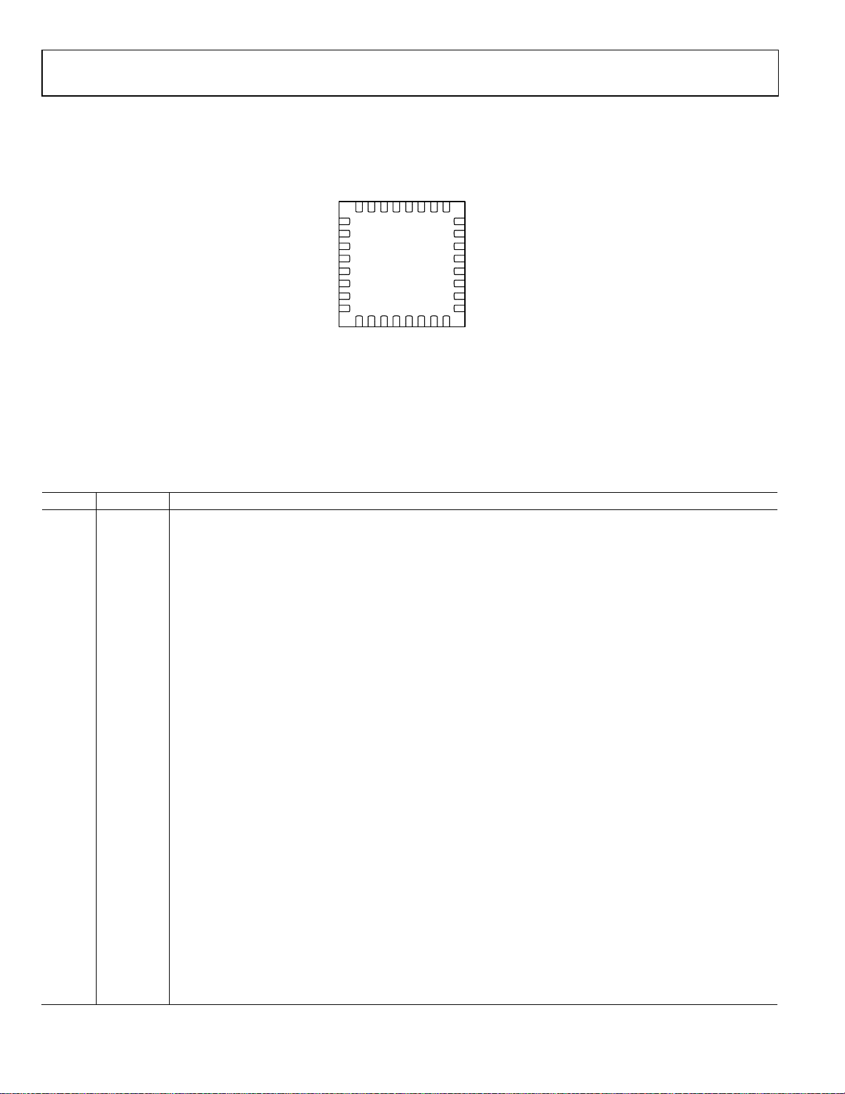
Available in 32-lead, 5 mm × 5 mm LFCSP
IN
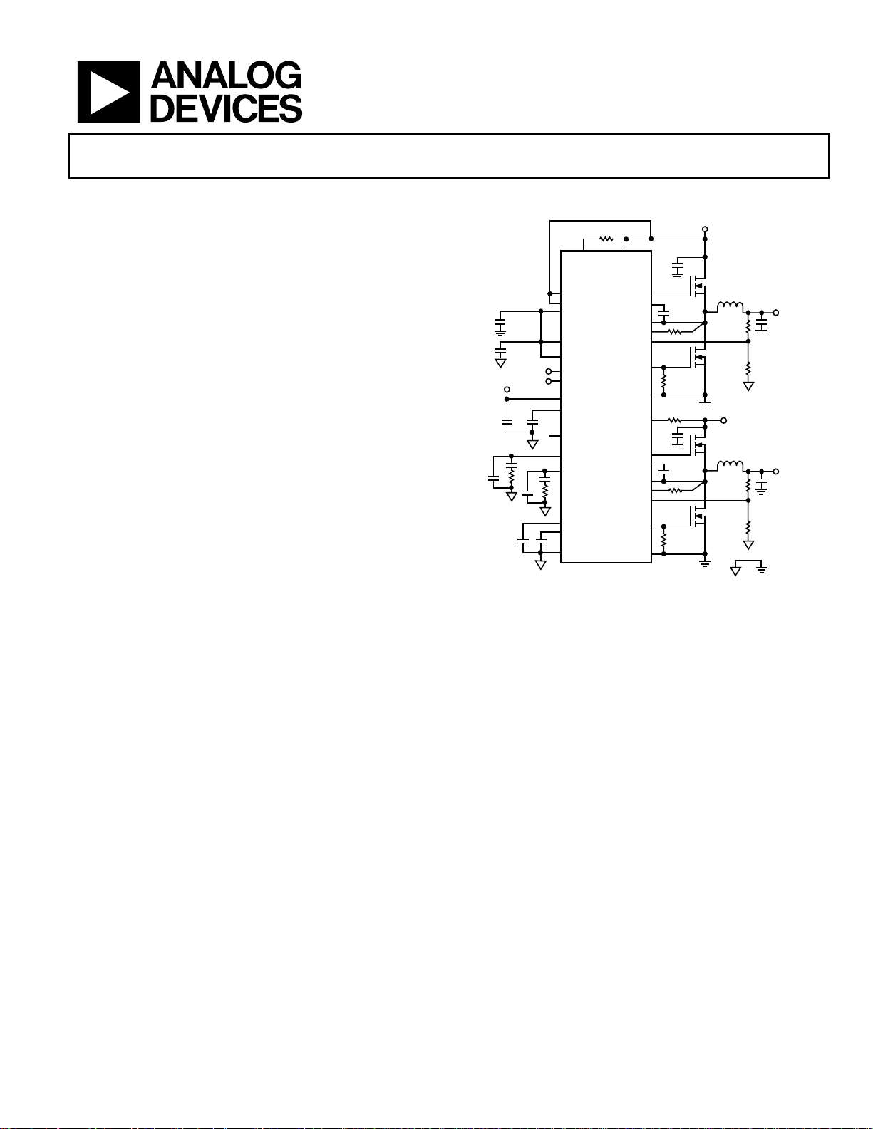
TYPICAL OPERATION CIRCUIT
APPLICATIONS
Consumer applications
Telecommunications base station and networking
Industrial and instrumentation
GENERAL DESCRIPTION
The ADP1876 is a dual output dc-to-dc synchronous buck
controller operating at 600 kHz fixed frequency with integrated
drivers that drive N-channel power MOSFETs. An additional
fixed voltage output, 150 mA linear regulator is available for
powering low power loads. The device operates in current
mode for improved transient response and uses valley current
Rev. A
Information furnished by Analog Devices is believed to be accurate and reliable. However, no
responsibility is assumed by Analog Devices for its use, nor for any infringements of patents or other
rights of third parties that may result from its use. Spe cifications subject to change without n otice. No
license is granted by implication or otherwise under any patent or patent rights of Analog Devices.
Trademarks and registered trademarks are the property of their respective owners.
Figure 1.
sensing for enhanced noise immunity. The two PWM outputs
are phase shifted 180° for reducing the input current ripple and
the required input capacitance.
The ADP1876 provides high speed, high peak current drive
capability with dead time optimization to enable energy
efficient power conversion.
One Technology Way, P.O. Box 9106, Norwood, MA 02062-9106, U.S.A.
Tel: 781.329.4700
Fax: 781.461.3113 ©2011 Analog Devices, Inc. All rights reserved.
www.analog.com
Page 2

ADP1876 Data Sheet
TABLE OF CONTENTS
Features .............................................................................................. 1
Applications ....................................................................................... 1
Typical Operation Circuit ................................................................ 1
General Description ......................................................................... 1
Revision History ............................................................................... 2
Functional Block Diagram .............................................................. 3
Specifications ..................................................................................... 4
Absolute Maximum Ratings ....................................................... 7
ESD Caution .................................................................................. 7
Pin Configuration and Function Descriptions ............................. 8
Typical Performance Characteristics ........................................... 10
Theory of Operation ...................................................................... 14
Independent Low Dropout Linear Regulator ......................... 14
Controller Architecture ............................................................. 14
Input Undervoltage Lockout ..................................................... 14
Internal Linear Regulator (VCCO) .......................................... 14
Overvoltage Protection .............................................................. 15
Power Good ................................................................................. 15
Short-Circuit and Current-Limit Protection .......................... 15
Shutdown Control ...................................................................... 15
Thermal Overload Protection ................................................... 16
Applications Information .............................................................. 17
Independent Low Dropout Linear Regulator ......................... 17
Setting the Output Voltage of the Controller ......................... 17
Soft Start ...................................................................................... 17
Setting the Current Limit .......................................................... 17
Accurate Current-Limit Sensing .............................................. 17
Setting the Slope Compensation .............................................. 18
Setting the Current Sense Gain ................................................ 18
Input Capacitor Selection .......................................................... 18
Input Filter .................................................................................. 19
Boost Capacitor Selection ......................................................... 19
Inductor Selection ...................................................................... 19
Output Capacitor Selection....................................................... 19
MOSFET Selection ..................................................................... 20
Loop Compensation .................................................................. 21
Switching Noise and Overshoot Reduction ............................ 22
PCB Layout Guideline ............................................................... 23
Typical Applications Circuit ..................................................... 23
Packaging and Ordering Information ......................................... 24
Outline Dimensions ................................................................... 24
Ordering Guide .......................................................................... 24
REVISION HISTORY
11/11—Rev. 0 to Rev. A
Added Evaluation Board to Ordering Guide .............................. 24
9/11—Revision 0: Initial Version
Rev. A | Page 2 of 24
Page 3
Data Sheet ADP1876
DUPLICATE FOR
CHANNEL 2
BST1
PGND1
+
–
+
–
+
–
+
–
+
–
+
–
FB2
0.6V
OV
UV
PGOOD1
CURRENT SENSE
AMPLIFIER
DH1
DL1
ILIM2
SW1
V
REF
= 0.6V
6.5µA
+
+
–
ERROR
AMPLIFIER
FB1
COMP1
SS1
PWM
COMPARATOR
DL
DRIVER
SLOPE COMP AND
RAMP GENERATOR
CURRENT-
LIMIT
CONTROL
VCCO
RAMP1
50µA
3.2V
g
m
OV1
+
TRK1
CS GAIN
DRIVER LOGIC
CONTROL AND
STATE
MACHINE
OVER_LIM1
PULSE SKIP
OVER_LIM1
LDO
LOGIC
EN1
EN2
VIN
UVLO
OSCILLATOR
600kHz
LINEAR
REGULATOR
VOUTLDO
VINLDO
PH1
PH2
REF
VCCO
OV
UV
0.6V
THERMAL
SHUTDOWN
AGND
0.6V
+
–
+
–
VCCO
ADP1876
VDL
FAULT
OV1
LOGIC
OVER_LIM1
OV1
EN1
EN1_SW
LOGIC
UV1
1kΩ
0.9V
DCM
ZERO CRO S S
DETECT
12kΩ
AV = 3, 6, 12, 24
VCCO
EN1_SW
EN2_SW
NC
–
+
10103-002
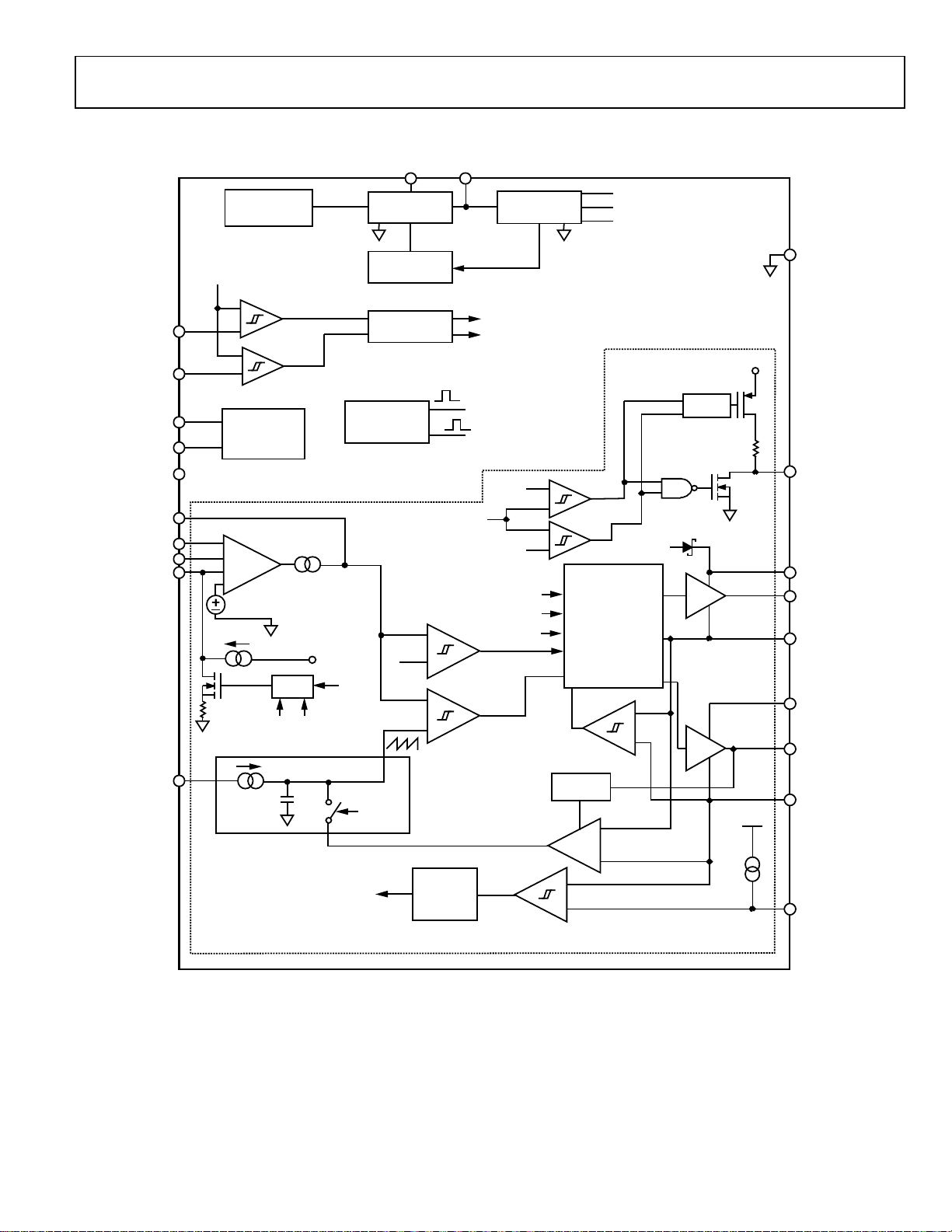
FUNCTIONAL BLOCK DIAGRAM
Figure 2. Functional Block Diagram
Rev. A | Page 3 of 24
Page 4

ADP1876 Data Sheet
CSG
OSC
VCCO
BST
SPECIFICATIONS
All limits at temperature extremes are guaranteed via correlation using standard statistical quality control. VIN = 12 V. The specifications
are valid for T
Table 1.
Parameter Symbol Test Conditions/Comments Min Typ Max Unit
POWER SUPPLY
Input Voltage VIN 2.75 20 V
Undervoltage Lockout Threshold IN
VIN falling 2.4 2.5 2.6
Undervoltage Lockout Hysteresis 0.1 V
Quiescent Current IIN EN1 = EN2 = VIN = 12 V, VFB = V
Shutdown Current I
ERROR AMPLIFIER
FB Input Bias Current IFB −100 +1 +100 nA
Transconductance gm Sink or source 1 µA 385 550 715 µS
TRK1 Input Bias Current I
CURRENT SENSE AMPLIFIER GAIN ACS Gain resistor connected to DLx,
Gain resistor connected to DLx,
Default setting, R
Gain resistor connected to DLx,
OUTPUT CHARACTERICTISTICS
Feedback Accuracy Voltage VFB TJ = −40°C to +85°C, VFB = 0.6 V −0.85% +0.6 +0.85% V
TJ = −40°C to +125°C, VFB = 0.6 V −1.5% +0.6 +1.5% V
Line Regulation of PWM ΔVFB/ΔVIN ±0.015 %/V
Load Regulation of PWM ΔVFB/ΔV
Oscillator Frequency f
LINEAR REGULATOR VCCO
VCCO Output Voltage TA = 25°C, I
TJ = −40°C to +125°C 4.7 5.0 5.3 V
VCCO Load Regulation I
VCCO Line Regulation VIN = 5.5 V to 20 V, I
VCCO Short-Circuit Current1 VCCO < 0.5 V 370 400 mA
VIN to VCCO Dropout Voltage2 V
LOGIC INPUTS
EN1, EN2 Threshold EN1/EN2 rising 0.57 0.63 0.68 V
EN1, EN2 Hysteresis 0.03 V
EN1, EN2 Input Leakage Current IEN VIN = 2.75 V to 20 V 1 200 nA
GATE DRIVERS (DHx, DLx PINS)
DHx Rise Time CDH = 3 nF, V
DHx Fall Time CDH = 3 nF, V
DLx Rise Time CDL = 3 nF 16 ns
DLx Fall Time CDL = 3 nF 14 ns
DHx to DLx Dead Time External 3 nF capacitor is connected to
= −40°C to +125°C, unless otherwise specified. Typical values are at TA = 25°C.
J
VIN rising 2.45 2.6 2.75 V
UVLO
CCO
(no switching)
EN1 = EN2 = GND, VIN = 5.5 V or 20 V 100 200 µA
IN_SD
0 V < V
TRK
R
R
R
V
COMP
CSG
CSG
COMP
< 1.5 V −100 +1 +100 nA
TRK1
= 47 kΩ ± 5%
= 22 kΩ ± 5%
= open 10.5 12 13.5 V/V
CSG
= 100 kΩ ± 5%
range 0.9 V to 2.2 V ±0.3 %
475 600 690 kHz
= 100 mA 4.8 5.0 5.18 V
= 0 mA to 100 mA, 35 mV
VCCO
= 20 mA 10 mV
VCCO
DROPOUT
I
= 100 mA, VIN ≤ 5 V 0.33 V
VCCO
− VSW = 5 V 16 ns
− VSW = 5 V 14 ns
BST
DHx and DLx
4.5 5.9 mA
2.4 3 3.6 V/V
5.2 6 6.9 V/V
20.5 24 26.5 V/V
25 ns
Rev. A | Page 4 of 24
Page 5
Data Sheet ADP1876
Parameter Symbol Test Conditions/Comments Min Typ Max Unit
DHx or DLx Driver RON, Sourcing
Current
1
R
DHx or DLx Driver RON, Tempco TC
DHx or DLx Driver RON, Sinking
Current
1
R
DHx Maximum Duty Cycle f
Minimum DHx On Time 130 ns
Minimum DHx Off Time 340 ns
Minimum DLx On Time 290 ns
COMP VOLTAGE RANGE V
THERMAL SHUTDOWN
Thermal Shutdown Threshold T
Thermal Shutdown Hysteresis 20 °C
OVERVOLTAGE AND POWER-GOOD
THRESHOLDS (FBx PINS)
FBx Overvoltage Threshold VOV V
FBx Overvoltage Hysteresis 40 mV
FBx Undervoltage Threshold VUV V
FBx Undervoltage Hysteresis 30 mV
FB1 TO TRK1 OFFSET VOLTAGE
SOFT START (SSx Pins)
SSx Output Current ISS During start-up 4.6 6.5 8.4 μA
SSx Pull-Down Resistor During a fault condition 1 kΩ
POWER GOOD (PGOODx Pins)
PGOODx Pull-up Resistor R
PGOODx Delay 12 μs
Overvoltage or Undervoltage
Minimum Duration
ILIM1, ILIM2 Threshold Voltage1 Relative to PGNDx −5 0 +5 mV
ILIM1, ILIM2 Output Current ILIMx = PGNDx 40 50 60 μA
Current Sense Blanking Period
INTEGRATED RECTIFIER
At 20 mA forward current 16 Ω
(BOOST DIODE) RESISTANCE
INDEPENDENT LOW DROPOUT
LINEAR REGULATOR
VINLDO Voltage Range V
VOUTLDO Voltage V
VOUTLDO Maximum Load V
Quiescent Current I
INLDO
Line Regulation ΔV
Load Regulation ΔV
Power Supply Rejection Ratio PSRR
Sourcing 2 A with a 100 ns pulse 2 Ω
ON_SOURCE
Sourcing 1 A with a 100 ns pulse,
2.3 Ω
VIN = 3 V
V
RON
Sinking 2 A with a 100 ns pulse 1.5 Ω
ON_SINK
0.85 2.3 V
COMP
155 °C
TMSD
Internal pull-up resistor to VCCO 12.5 kΩ
PGOOD
= 3 V or 12 V 0.3 %/°C
IN
Sinking 1 A with a 100 ns pulse,
= 3 V
V
IN
= 600 kHz 76 %
OSC
rising 0.67 0.7 0.73 V
FB
rising 0.51 0.54 0.57 V
FB
TRK1 = 0.3 V to 0.55 V,
− V
offset = V
FB
TRK
This is the minimum duration
2 Ω
−120 +50 mV
12 μs
required to trip the PGOODx signal
After DLx goes high, current limit is
100 ns
not sensed during this period
Input range 2.7 5.5 V
INLDO
OUTLDO
= 2.7 V to 5.5 V, I
V
INLDO
OUTLDO
= 1 mA to
1.47 1.5 1.53 V
150 mA
V
OUTLDO
= 2.7 V to 5.5 V 150 mA
INLDO
= 2.7 V to 5.5 V, no load at
V
INLDO
30 60 μA
output
OUTLDO
OUTLDO
I
= 150 mA, V
OUTLDO
= 2.7 V to 5.5 V, I
V
INLDO
= 2.7 V to 5.5 V 0.3 %
INLDO
OUTLDO
= 1 mA to
0.4 %
150 mA
1 kHz, V
= 2.7 V to 5.5 V,
INDLO
70 dB
10 mA load
Rev. A | Page 5 of 24
Page 6

ADP1876 Data Sheet
Parameter Symbol Test Conditions/Comments Min Typ Max Unit
RMS Output Noise N 10 Hz to 100 kHz, VINLDO = 5 V 40 µV rms
Short-Circuit Current V
Undervoltage Lockout Threshold V
INLDO_UVLO
Undervoltage Lockout Hysteresis V
1
Guaranteed by design. Not production tested.
2
Connect VIN to VCCO when VIN < 5.5 V.
V
= GND 400 mA
OUTLDO
rising 2.35 2.5 2.65 V
INLDO
0.18 V
INLDO
Rev. A | Page 6 of 24
Page 7
Data Sheet ADP1876
Stresses a bove those l isted under Absolute Maximum Ratings
may cause permanent damage to the device. This is a stress
rating only; functional operation of the device at these or any
other conditions above those indi cated in the operational
section of this specification is not implied. Exposure to absolute
maximum rating conditions for extended periods may affect
device reliability.
ABSOLUTE MAXIMUM RATINGS
Table 2.
Parameter Rating
VIN, EN1/EN2, RAMP1/RAMP2 21 V
FB1/FB2, COMP1/COMP2, SS1/SS2, TRK1,
VINLDO, VOUTLDO, VCCO, VDL,
PGOOD1/PGOOD2
ILIM1/ILIM2 −0.3 V to +21 V
BST1/BST2 to SW1/SW2 −0.3 V to +6 V
BST1/BST2, DH1/DH2, SW1/SW2 to
PGND1/PGND2
DL1/DL2 to PGND1/PGND2 −0.3 V to VCCO + 0.3 V
BST1/BST2 to PGND1/PGND2, SW1/SW2 to
PGND1/PGND2 (20 ns Transients)
SW1, SW2 to PGND1, PGND2
(20 ns Transients)
DL1/DL2, SW1/SW2, ILIM1/ILIM2 to
PGND1/PGND2 (20 ns Negative Transients)
PGND1/PGND2 to AGND −0.3 V to +0.3 V
PGND1/PGND2 to AGND (20 ns Transients) −8 V to +4 V
θJA, Multilayer PCB (Natural Convection)
1, 2
Operating Junction Temperature Range3 −40°C to +125°C
Storage Temperature Range −65°C to +150°C
Maximum Soldering Lead Temperature 260°C
1
Measured with exposed pad attached to the printed circuit board (PCB).
2
Junction-to-ambient thermal resistance (θJA) of the package was calculated
or simulated on a multilayer PCB.
3
The junction temperature, TJ, of the device is dependent on the ambient
temperature, T
ambient thermal resistance of the package, θ
temperature is calculated from the ambient temperature and power
dissipation using the formula, T
, the power dissipation of the device, PD, and the junction to
A
= TA + PD × θJA.
J
−0.3 V to +6 V
−0.3 V to +28 V
32 V
25 V
−8 V
32.6°C/W
. Maximum junction
JA
Absolute maximum ratings apply individually only, not in
combination. Unless otherwise specified, all other voltages are
referenced to GND.
ESD CAUTION
Rev. A | Page 7 of 24
Page 8
ADP1876 Data Sheet
Enable Input for Channel 1. Drive EN1 high to turn on the Channel 1 controller, and drive it low to turn it off. Tie EN1
to VIN for automatic startup. For a precision UVLO, put an appropriately sized resistor divider from VIN to AGND and
to VIN for automatic startup. For a precision UVLO, put an appropriately sized resistor divider from VIN to AGND and
24
SW1
23
DH1
22
PGND1
21
DL1
20
DL2
19
PGND2
18
DH2
17
SW2
1
2
3
4
5
6
7
8
EN1
VIN
VINLDO
VOUTLDO
VCCO
VDL
AGND
NC
9
10111213141516
EN2
FB2
COMP2
RAMP2
SS2
PGOOD2
ILIM2
BST2
32313029282726
25
TRK1
FB1
COMP1
RAMP1
SS1
PGOOD1
ILIM1
BST1
ADP1876
TOP VIEW
(Not to S cale)
NOTES
1. NC = NO CO NNE C T. DO NOT CONNECT TO THIS PIN.
2. CONNECT THE BOTTOM EXPOSED PAD OF THE
LFCSP PACKAGE TO SYSTEM AGND PLANE .
10103-003
PIN CONFIGURATION AND FUNCTION DESCRIPTIONS
Figure 3. Pin Configuration
Table 3. Pin Function Descriptions
Pin No. Mnemonic Description
1 EN1
tie the midpoint to this pin.
2 VIN Connect to Main Power Supply. Bypass with a 1 μF or larger ceramic capacitor connected as close to this pin as
possible and PGNDx.
3 VINLDO Input for Independent Linear Dropout (LDO) Regulator.
4 VOUTLDO Output for Independent LDO Regulator.
5 VCCO Output of the Internal LDO. The internal circuitry and gate drivers are powered from VCCO. Bypass VCCO to AGND
with a 1 μF or larger ceramic capacitor. The VCCO output is always active, even during fault conditions, and it
cannot be turned off even when EN1 or EN2 is low. For operation at VIN below 5 V, VIN can be jumped to VCCO. Do
not use the VCCO to power any other auxiliary system load.
6 VDL Power Supply for the Low-Side Driver. Bypass VDL to PGNDx with a 1 μF ceramic capacitor. Connect VCCO to VDL.
7 AGND Analog Ground.
8 NC No connect. Do not connect to this pin.
9 EN2 Enable Input for Channel 2. Drive EN2 high to turn on the Channel 2 controller, and drive it low to turn off. Tie EN2
tie the midpoint to this pin.
10 FB2 Output Voltage Feedback for Channel 2.
11 COMP2 Compensation Node for Channel 2. Output of the Channel 2 error amplifier. Connect a series resistor/capacitor
network from COMP2 to AGND to compensate the regulation control loop.
voltage at RAMP2 is 0.2 V during operation. This pin is high impedance when the channel is disabled.
internally pulled up to 3.2 V through a 6.5 µA current source.
PGOOD2 and VCCO. PGOOD2 is pulled to ground when the Channel 2 output is outside the regulation window. An
external pull-up resistor is not required.
the current-limit offset. For accurate current-limit sensing, connect ILIM2 to a current sense resistor at the source of
12 RAMP2 Programmable Current Setting for Slope Compensation of Channel 2. Connect a resistor from RAMP2 to VIN. The
13 SS2 Soft Start Input for Channel 2. Connect a capacitor from SS2 to AGND to set the soft start period. This node is
14 PGOOD2 Open-Drain Power-Good Indicator Logic Output at PGOOD2. An internal 12 kΩ resistor is connected between
15 ILIM2 Current-Limit Sense Comparator Inverting Input for Channel 2. Connect a resistor between ILIM2 and SW2 to set
the low-side MOSFET.
16 BST2 Boot Strapped Upper Rail of High-Side Internal Driver for Channel 2. Connect a 0.1 µF to 0.22 µF multilayer ceramic
capacitor (MLCC) between BST2 and SW2. There is an internal boost rectifier connected between VDL and BST2.
Rev. A | Page 8 of 24
Page 9

Data Sheet ADP1876
Pin No. Mnemonic Description
17 SW2 Switch Node for Channel 2. Connect to the source of the high-side N-channel MOSFET and the drain of the low-
side N-channel MOSFET of Channel 2.
18 DH2 High-Side Switch Gate Driver Output for Channel 2.
19 PGND2 Power Ground for Channel 2. Ground for Internal Channel 2 driver. Differential current is sensed between SW2 and
PGND2. Directly shorting PGND2 to PGND1 is not recommended.
20 DL2 Low-Side Synchronous Rectifier Gate Driver Output for Channel 2. To set the gain of the current sense amplifier,
connect a resistor between DL2 and PGND2.
21 DL1 Low-Side Synchronous Rectifier Gate Driver Output for Channel 1. To set the gain of the current sense amplifier,
connect a resistor between DL1 and PGND1.
22 PGND1 Power Ground for Channel 1. Ground for internal Channel 1 driver. Differential current is sensed between SW1 and
PGND1. Directly shorting PGND2 to PGND1 is not recommended.
23 DH1 High-Side Switch Gate Driver Output for Channel 1.
24 SW1 Power Switch Node for Channel 1. Connect SW1 to the source of the high-side N-channel MOSFET and the drain of
the low-side N-channel MOSFET of Channel 1.
25 BST1 Boot Strapped Upper Rail of High-Side Internal Driver for Channel 1. Connect a 0.1µF to 0.22 µF multilayer ceramic
capacitor (MLCC) between BST1 and SW1. There is an internal boost diode or rectifier connected between VDL
and BST1.
26 ILIM1 Current-Limit Sense Comparator Inverting Input for Channel 1. Connect a resistor between ILIM1 and SW1 to set
the current-limit offset. For accurate current-limit sensing, connect ILIM1 to a current sense resistor at the source of
the low-side MOSFET.
27 PGOOD1 Open-Drain Power-good Indicator Logic Output. PGOOD1 includes an internal 12 kΩ resistor connected between
PGOOD1 and VCCO. PGOOD1 is pulled to ground when the Channel 1 output is outside the regulation window. An
external pull-up resistor is not required.
28 SS1 Soft Start Input for Channel 1. Connect a capacitor from SS1 to AGND to set the soft start period. This node is
internally pulled up to 3.2 V through a 6.5 µA current source.
29 RAMP1 Programmable Current Setting for Channel 1 Slope Compensation. Connect a resistor from RAMP1 to VIN. The
voltage at RAMP1 is 0.2 V during operation. This pin is high impedance when the channel is disabled.
30 COMP1 Compensation Node For Channel 1. Output of Channel 1 error amplifier. Connect a series resistor/capacitor
network from COMP1 to AGND to compensate the regulation control loop.
31 FB1 Output Voltage Feedback for Channel 1.
32 TRK1 Tracking Input for Channel 1.
Rev. A | Page 9 of 24
Page 10

ADP1876 Data Sheet
0
10
20
30
40
50
60
70
80
90
100
0 2 4 6 8 10 12 14
EFFICIENCY (%)
LOAD (A)
V
IN
= 12V
V
OUT
= 1.8V
V
OUT
= 5V
10103-004
–0.25
–0.20
–0.15
–0.10
–0.05
0
2.5 3.0 3.5 4.0 4.5 5.0
ΔVCCO (V)
VIN (V)
50mA LOAD
100mA LOAD
10103-005
4.65
4.70
4.75
4.80
4.85
4.90
4.95
5.00
5.05
5.10
5 7 9 11 13 15 17
Δ VCCO (V)
VIN (V)
NO LOAD O N LDO
100mA LOAD ON LDO
10103-006
0
1
2
3
4
5
6
0
1 2 3 4 5 6
VCCO (V)
V
IN
(V)
10103-007
10103-008
CH1 5.00A Ω
CH3 20.0mV
M100µs A CH1 9.00A
1
3
VOUT1 = 5V OUTPUT RESPONSE
OUTPUT S TEP LOAD = 5A T O 10A
2
CH3 1V
CH2 5VCH1 5V
CH4 1A Ω
M1ms A CH1 2.4V
VIN = 12V
V
OUT
= 1.8V
OUTPUT P RE CHARGED TO 1V
DH1
DL1
VOUT1
IL1
1
3
4
10103-009
TYPICAL PERFORMANCE CHARACTERISTICS
Test conditions are at TA = 25°C and VIN = 12 V, unless otherwise specified.
Figure 4. Efficiency Plot of Figure 33
Figure 5. VCCO Dropout
Figure 7. VCCO vs. VIN
Figure 8. Step Load Transient of Figure 33
Figure 6. VCCO Line Regulation
Figure 9. Soft Start Into Precharged Output
Rev. A | Page 10 of 24
Page 11

Data Sheet ADP1876
CH3 1V
CH2 2VCH1 10V
CH4 1V
M10ms A CH2 1.52V
CSS = 100nF
V
OUT
(CH3)
SS (CH4)
EN
SW
1
2
3
4
10103-010
10103-011
CH1 10.0V
B
W
CH3 2.00V
B
W
M10.0ms A CH4 800mV
4
2
1
CH2 2.00V
B
W
CH4 1.00V
B
W
SW1
VOUT1 (PRE LOADED)
VOUTLDO
VCCO
–0.8
–0.6
–0.4
–0.2
0
0.2
0.4
0.6
2.5 5.0 7.5 10.0 12.5 15.0 17.5 20.0
CHANGE IN f
SW
(%)
V
IN
(V)
600kHz
REFERENCE AT V
IN
= 2.75V
10103-012
–2.5
–2.0
–1.5
–1.0
–0.5
0
0.5
1.0
1.5
2.0
–40 –15 10 35 60 85 110 135
CHANGE IN
f
SW
(%)
TEMPERATURE (°C)
V
IN
= 12V; REFERENCEDAT 25°C
10103-013
50
100
150
200
250
300
350
2.5 5.0 7.5 10.0 12.5 15.0 17.5 20.0
TIME (ns)
VIN (V)
DHx MINIMUM OFF TIME
DHx MINIMUM ON TIME
10103-014
–4
–3
–2
–1
0
1
2
3
4
–40 –15 10 35 60 85 110 135
CHANGE IN MINIMUM ON/OFF TIME (%)
TEMPERATURE (°C)
DHx MINIMUM ON TIME
DHx MINIMUM OFF TIME
10103-015
Figure 10. Enable Startup Function
Figure 11. Thermal Shutdown Waveform
Figure 13. fSW vs. Temperature
Figure 14. Typical DHx Minimum On Time and Off Time
Figure 12. Change in fSW vs. VIN
Figure 15. DHx Minimum On Time and Off Time Over Temperature
Rev. A | Page 11 of 24
Page 12

ADP1876 Data Sheet
25
35
34
33
32
31
30
29
28
27
26
–40 –20 0 20 40 60 80 100 120 140
DEAD TIME ( ns)
TEMPERATURE (°C)
VIN = 12V
OUTPUT IS LOADED
HS FET = BS C080N03LS
LS FET = BS C030N03LS
DEAD TIME BETWEEN SWx FALLING EDGE
AND DLx RISING EDGE, I NCLUDING DIODE RE COVERY TIME
10103-016
25
45
43
41
39
37
35
33
31
29
27
0 2015105
DEAD TIME ( ns)
V
IN
(V)
T
A
= 25°C
OUTPUT IS LOADED
HS FET = BS C080N03LS
LS FET = BS C030N03LS
DEAD TIME BETWEEN SWx FALLING EDGE
AND DLx RISING EDGE, I NCLUDING DIODE RE COVERY TIME
10103-017
400
420
440
460
480
500
520
540
560
580
600
–40 –15 10 35 60 85 110 135
g
m
(µS)
TEMPERATURE (°C)
VIN = 2.75V TO 20V
10103-018
0
0.5
1.0
1.5
2.0
2.5
3.0
3.5
4.0
4.5
–40 –15 10 35 60 85 110 135
DRIVER RESI STANCE (Ω)
TEMPERATURE (°C)
V
IN
= 2.75V, SOURCING
V
IN
= 12V, SOURCING
V
IN
= 2.75V, SINKING
VIN = 12V, SINKING
10103-019
0
0.005
0.010
0.015
0.020
0.025
0.030
0.035
3.0 3.5 4.0 4.5 5.0 5.5 6.0
LINE REGULATION (%)
VINLDO (V)
10103-020
–0.20
–0.18
–0.16
–0.14
–0.12
–0.10
–0.08
–0.06
–0.04
–0.02
0
0 0.025 0.050 0.075 0.100 0.125 0.150 0.175 0.200
LOAD REGUL ATION (%)
VOUTLDO LOAD (A)
VINLDO = 3V
VINLDO = 5V
10103-021
Figure 16. Dead Time vs. Temperature
Figure 17. Dead Time vs. VIN
Figure 19. Driver Resistance vs. Temperature
Figure 20. VOUTLDO Line Regulation
Figure 18. gm of Error Amplifier vs. Temperature
Figure 21. VOUTLDO Load Regulation
Rev. A | Page 12 of 24
Page 13

Data Sheet ADP1876
0
5
10
15
20
25
30
35
10µ 100µ 1m 10m 100m 1
RMS NOISE (µV)
VOUTLDO LOAD (A)
10103-022
10103-023
CH1 100mA Ω
B
W
M10.0µs A CH1 118mA
2
1
CH2 50.0mV
B
W
STEP LOAD
1mA TO 200mA
CINLDO = 1µ F; COUTLDO = 4.7µF
OUTPUT TRANSIENT
Figure 22. VOUTLDO Noise Spectral Density
Figure 23. VOUTLDO Step Load Transient
Rev. A | Page 13 of 24
Page 14

ADP1876 Data Sheet
FF
OSC Q
Q
S
R
A
CS
V
CS
V
IN
V
IN
A
R
R
RAMP
I
RAMP
C
R
FROM
ERROR AMP
TO
DRIVERS
FROM
LOW SIDE
MOSFET
10103-024
THEORY OF OPERATION
The ADP1876 is a dual output dc-to-dc synchronous buck
controller with integrated drivers that drive N-channel power
MOSFETs. The device operates in current mode for improved
transient response and uses valley current sensing for enhanced
noise immunity. The two outputs are phase shifted 180°. This
reduces the input current ripple and the required input
capacitance.
The integrated boost diodes in the ADP1876 reduce the overall
system cost and component count. The ADP1876 operates at a
fixed frequency of 600 kHz and includes programmable soft
start, current limit, and power good.
INDEPENDENT LOW DROPOUT LINEAR REGULATOR
In addition to the dual channel step-down controller, a standalone linear dropout (LDO) voltage regulator with a fixed output
of 1.5 V is built into the ADP1876 and operates independently
from the controllers. The output of the LDO delivers up to
150 mA to the load. See the Applications Information section
for more information.
CONTROLLER ARCHITECTURE
The ADP1876 is based on a fixed frequency, current mode
PWM control architecture. The inductor current is sensed by
the voltage drop measured across the external low-side MOSFET
R
during the off period of the switching cycle (valley inductor
DSON
current). The current sense signal is further processed by the
current sense amplifier. The output of the current sense amplifier is
held, and the emulated current ramp is multiplexed and fed into
the PWM comparator (see Figure 24). The valley current
information is captured at the end of the off period, and the
emulated current ramp is applied at that point when the next on
cycle begins. An error amplifier integrates the error between the
feedback voltage and the generated error voltage from the
COMP pin (see the “from error amp” in Figure 24).
As shown in Figure 24, the emulated current ramp is generated
inside the IC but offers programmability through the RAMPx
pin (see Figure 1 for the typical operation circuit). Selecting an
appropriate value resistor from V
to the RAMPx pin programs
IN
a desired slope compensation value and, at the same time,
provides a feedforward feature. The benefits realized by
deploying this type of control scheme are as follows:
• The turn-on current spike does not corrupt the current ramp.
• The current signal is stable because the current signal is
sampled at the end of the turn-off period, which gives time
for the switch node ringing to settle.
The normal benefits of using current mode control scheme still
apply, such as simplicity of loop compensation. Control logic
enforces antishoot through operation to limit cross conduction of
the internal drivers and external MOSFETs.
Synchronous Rectifier and Dead Time
The synchronous rectifier (low-side MOSFET) improves efficiency
by replacing the Schottky diode that is normally used in an
asynchronous buck regulator. In the ADP1876, the antishoot
through circuit monitors the SW and DL nodes and adjusts the
low-side and high-side drivers to ensure break-before-make
switching to prevent cross conduction or shoot through between
the high-side and low-side MOSFETs. This break-before-make
switching is known as the dead time, which is not fixed and
depends on how fast the MOSFETs are turned on and off. In a
typical application circuit that uses medium sized MOSFETs
with input capacitance of approximately 3 nF, the typical dead
time is approximately 30 ns. When small and fast MOSFETs are
used, the dead time can be as low as 13 ns.
INPUT UNDERVOLTAGE LOCKOUT
When the bias input voltage, VIN, is less than the undervoltage
lockout (UVLO) threshold, the switch drivers stay inactive.
When V
switching.
exceeds the UVLO threshold, the switchers begin
IN
INTERNAL LINEAR REGULATOR (VCCO)
The internal linear regulator is low dropout, meaning it can
regulate its output voltage, VCCO. VCCO powers the internal
control circuitry and provides power for the gate drivers. It is guaranteed to have more than 200 mA of output current capability,
which is sufficient to handle the gate drive requirements of
typical logic threshold MOSFETs. VCCO is always active and
cannot be shut down by the EN1/EN2 pins. Bypass VCCO to
AGND with a 1 µF or greater capacitor.
Because the LDO supplies the gate drive current, the output of
VCCO is subject to sharp transient currents as the drivers switch
and the boost capacitors recharge during each switching cycle.
Rev. A | Page 14 of 24
Figure 24. Simplified Control Architect ure
Page 15

Data Sheet ADP1876
VIN = 2.75V TO 5.5V
ADP1876
VIN VCCO
10103-025
CH3 500mV
CH1 10V
CH4 10A Ω
M2ms A CH1 11.2V
SW1
SS1
INDUCTOR CURRENT
1
3
4
10103-026
ADP1876
FB1
OR
FB2
EN1
OR
EN2
R
TOP
R
BOT
V
OUT1
R1
R2
MASTER
SUPPLY VOLTAGE
10103-027
The LDO has been optimized to handle these transients without
overload faults. Due to the gate drive loading, using the VCCO
output for other external auxiliary system loads is not recommended.
The LDO includes a current limit well above the expected
maximum gate drive load. This current limit also includes a
short-circuit fold back to further limit the VCCO current in the
event of a short-circuit fault.
The VDL pin provides power to the low-side driver. Connect
VDL to VCCO. Bypass VDL to PGND with a 1 µF (minimum)
ceramic capacitor, which must be placed close to the VDL pin.
For an input voltage of less than 5.5 V, it is recommended to
bypass the LDO by connecting VIN to VCCO, as shown in
Figure 25, thus eliminating the dropout voltage. However, for
example, if the input range is 4 V to 7 V, the LDO cannot be
bypassed by shorting VIN to VCCO because the 7 V input has
exceeded the maximum voltage rating of the VCCO pin. In this
case, use the LDO to drive the internal drivers noting that there
is a dropout when V
is less than 5 V.
IN
SHORT-CIRCUIT AND CURRENT-LIMIT PROTECTION
When the output is shorted or the output current exceeds the
current limit set by the current-limit setting resistor (between
ILIMx and SWx) for eight consecutive cycles, the ADP1876
shuts off both the high-side and low-side drivers and restarts
the soft start sequence every 10 ms, which is known as hiccup
mode. The SS node discharges to zero through an internal 1 kΩ
resistor during an overcurrent or short-circuit event. Figure 26
shows that the ADP1876 (a 20 A application circuit) is entering
current-limit hiccup mode when the output is shorted.
Figure 25. Configuration for V
< 5.5 V
IN
OVERVOLTAGE PROTECTION
The ADP1876 operates at a 600 kHz fixed frequency PWM.
When the output is shorted to a voltage higher than the regulation voltage, the duty cycle of the controller modulates to keep
the output stable at the preset regulation voltage by sinking
current through the low-side N-channel MOSFET during the
off cycle.
POWER GOOD
The PGOODx pin is an open-drain NMOS with an internal
12 kΩ pull-up resistor connected between PGOODx and
VCCO. PGOODx is internally pulled up to VCCO during
normal operation and is active low when tripped. When the
feedback voltage, V
drops below the undervoltage threshold, the PGOODx output
is pulled to ground after a delay of 12 µs. The overvoltage or undervoltage condition must exist for more than 12 µs for PGOODx to
become active. The PGOODx output also becomes active if a
thermal overload condition is detected.
, rises above the overvoltage threshold or
FB
Figure 26. Current-Limit Hiccup Mode, 20 A Circuit
SHUTDOWN CONTROL
The EN1 and EN2 pins enable or disable Channel 1 and
Channel 2, respectively, of the ADP1876. The precision enable
threshold for EN1 or EN2 is typically 0.63 V. When the EN1
or EN2 voltage rises above 0.63 V, the ADP1876 is enabled
and starts normal operation after the soft start period. When
the voltage at ENx drops below 0.57 V, the switchers and the
internal circuits in the ADP1876 are turned off. Note that
EN1/EN2 cannot shut down the VOUTLDO or VCCO, which
are always active.
For the purpose of start-up power sequencing, the startup of the
ADP1876 can be programmed by connecting an appropriate
resistor divider from the master power supply to the EN1 or
EN2 pin, as shown in Figure 27. For instance, if the desired
start-up voltage from the master power supply is 10 V, R1 and
R2 can be set to 156 kΩ and 10 kΩ, respectively.
Figure 27. Optional Power-Up Sequencing Circuit
Rev. A | Page 15 of 24
Page 16

ADP1876 Data Sheet
THERMAL OVERLOAD PROTECTION
The ADP1876 has an internal temperature sensor that senses
the junction temperature of the chip. When the junction temperature of the ADP1876 reaches approximately 155°C, the
ADP1876 enters thermal shutdown, where the converter,
VCCO, and VOUTLDO are turned off and SSx discharges
toward zero through an internal 1 kΩ resistor. When the
junction temperature drops below 135°C, the ADP1876
resumes normal operation after the soft start sequence.
Rev. A | Page 16 of 24
Page 17

Data Sheet ADP1876
−
=
FB
FB
OUT
BOTTOP
V
VV
RR
SSSS
Ct
A5.6
V6.0
µ
=
μA40
_ MAXDSON
LPK
ILIM
RIR×
=
APPLICATIONS INFORMATION
INDEPENDENT LOW DROPOUT LINEAR REGULATOR
The input voltage range to VINLDO of the independent LDO
regulator is 2.7 V to 5.5 V, and the output is fixed at 1.5 V with
a 150 mA maximum load current. The internal short-circuit
current limit is set to about 430 mA. Apply power to the VIN
pin to keep the LDO operating within specification. The LDO
is enabled when V
exceeds the input undervoltage lockout
INLDO
(UVLO) threshold. Safety features include short-circuit protection
and thermal overload shutdown.
SETTING THE OUTPUT VOLTAGE OF THE CONTROLLER
The output voltage is set using a resistive voltage divider from
the output to FBx. The voltage divider divides down the output
voltage to the 0.6 V FBx regulation voltage to set the regulation
output voltage. The output voltage can be set to as low as 0.6 V
and as high as 90% of the power input voltage.
The maximum input bias current into FBx is 100 nA. For a 0.15%
degradation in regulation voltage, and with 100 nA bias current,
the low-side resistor, R
in 67 µA of divider current. For R
, must be less than 9 kΩ, which results
BOT
, use a 1 kΩ to 20 kΩ resistor.
BOT
A larger value resistor can be used but results in a reduction in
output voltage accuracy due to the input bias current at the FBx
pin, whereas lower values cause increased quiescent current
consumption. Choose R
to set the output voltage by using
TOP
the following equation:
where:
R
is the high-side voltage divider resistance.
TOP
R
is the low-side voltage divider resistance.
BOT
V
is the regulated output voltage.
OUT
V
is the feedback regulation threshold, 0.6 V.
FB
The minimum output voltage is dependent on f
and minimum
SW
DHx on time. The maximum output voltage is dependent on
f
, the minimum DHx off time, the IR drop across the high-
SW
side N-channel MOSFET, and the DCR of the inductor.
SOFT START
The soft start period is set by an external capacitor between SS1
or SS2 and AGND. The soft start function limits the input inrush
current and prevents output overshoot.
When EN1/EN2 is enabled, a current source of 6.5 µA starts
charging the capacitor, and the regulation voltage is reached when
the voltage at SS1/SS2 reaches 0.6 V.
The soft start period is approximated by the following equation:
The SSx pin reaches a final voltage of 3.2 V. If the output voltage
is precharged prior to turn on, the ADP1876 prevents reverse
inductor current, which discharges the output capacitor. When
the voltage at SSx exceeds the regulation voltage (typically at
0.6 V), the reverse current is enabled to allow the output voltage
regulation to be independent of load current.
When a controller is disabled, for instance, EN1/EN2 is pulled
low or experiences an overcurrent limit condition, the soft start
capacitor is discharged through an internal 1 kΩ pull-down
resistor.
SETTING THE CURRENT LIMIT
The current-limit comparator measures the voltage across the
low-side MOSFET to determine the load current.
The current limit is set by an external current-limit resistor,
R
between ILIMx and SWx. The current sense pin, ILIMx,
ILIM,
sources nominally 50 μA to this external resistor. This creates an
offset voltage of R
across the low-side MOSFET R
multiplied by 50 μA. When the drop
ILIM
is equal to or greater than
DSON
this offset voltage, the ADP1876 flags a current-limit event.
Because the ILIMx current and the MOSFET R
vary over
DSON
process and temperature, set the minimum current limit to
ensure that the system can handle the maximum desired load
current. To do this, use the peak current in the inductor, which
is the desired output current-limit level, plus ½ of the ripple
current, the maximum R
of the MOSFET at its highest
DSON
expected temperature, and the minimum ILIM current. Keep in
mind that the temperature coefficient of the MOSFET R
DSON
is
typically 0.4%/°C.
where:
I
is the peak inductor current.
LPK
ACCURATE CURRENT-LIMIT SENSING
R
of the MOSFET can vary by more than 50% over the
DSON
temperature range. Accurate current-limit sensing is achieved
by adding a current sense resistor from the source of the lowside MOSFET to PGNDx. Make sure that the power rating of the
current sense resistor is adequate for the application. Apply the
previous equation and calculate R
with R
. See Figure 28 for the implementation of this
SENSE
accurate current-limit sensing scheme.
by replacing R
ILIM
DSON_MAX
Rev. A | Page 17 of 24
Page 18

ADP1876 Data Sheet
MAXDSONCS
RAMP
RA
L
R
_
10
106.3××
=
μA200
V2.0
μA6 ≤
−
≤
RAMP
IN
R
V
CSMINDSON
LPP
CSMIN
ARIV ××−=
_
2
1
V75.0
CSMAXDSON
LPP
LOADMAXCSMAX
ARIIV ××++=
_
)
2
1
(V75.0
( )
CSMAX
RAMP
ON
IN
COMPMAX
V
R
tV
V +
×
−
=
pF25
V2.0
V
IN
ADP1876
DHx
SWx
ILIMx
DLx
R
ILIM
R
SENSE
10103-028
PGNDx
V
IN
ADP1876
DHx
SWx
ILIMx
DLx
R
ILIM
R
CSG
RAMP
R
RAMP
10103-029
PGNDx
SETTING THE CURRENT SENSE GAIN
The voltage drop across the external low-side MOSFET is
sensed by a current sense amplifier by multiplying the peak
Figure 28. Accurate Current-Limit Sensing
SETTING THE SLOPE COMPENSATION
In a current mode control topology, slope compensation is
needed to prevent subharmonic oscillations in the inductor
current and to maintain a stable output. The external slope
compensation is implemented by summing the amplified sense
signal and a scaled voltage at the RAMPx pin. To implement the
slope compensation, connect a resistor between RAMPx and
the input voltage. The resistor, R
, is calculated by
RAMP
inductor current and the R
amplified by a gain factor of either 3 V/V, 6 V/V, 12 V/V, or
24 V/V, which is programmable by an external resistor, R
connected to the DLx pin. This gain is sensed during power-up
only and not during normal operation. The amplified voltage is
summed with the slope compensation ramp voltage and fed
into the PWM controller for a stable regulation voltage.
The voltage range of the internal node, V
and 2.2 V. Select the current sense gain such that the internal
minimum amplified voltage (V
maximum amplified voltage (V
or V
is not the same as V
CSMAX
to 2.3 V. Make sure that the maximum V
not exceed 2.2 V to account for temperature and device to
device variations. The following are equations for V
V
CSMAX
, and V
COMPMAX
:
of the MOSFET. The result is
DSON
, is between 0.4 V
CS
) is above 0.4 V and the
CSMIN
) is 2.1 V. Note that V
CSMAX
, which has a range of 0.85 V
COMP
(V
COMP
COMPMAX
CSMIN
,
CSG
CSMIN
) does
,
where:
3.6 × 10
10
is an internal parameter.
L is the inductance of the inductor.
R
A
is the the low-side MOSFET maximum on resistance.
DSON _MAX
is the gain, either 3 V/V, 6 V/V, 12 V/V, or 24 V/V, of the
CS
current sense amplifier (see the Setting the Current Sense Gain
section for more details).
Keep in mind that R
as much as 0.4%/
o
C. Choose R
temperature. The voltage at RAMPx is fixed at 0.2 V, and the
current going into RAMPx should be between 6 µA and 200 µA.
Ensure that the following condition is satisfied:
For instance, with an input voltage of 12 V, R
exceed 1.9 MΩ. If the calculated R
select an R
value that produces between 6 µA and 20 µA.
RAMP
Figure 29 illustrates the connection of the slope compensation
resistor, R
, and the current sense gain resistor, R
RAMP
Figure 29. Slope Compensation and CS Gain Connection
is temperature dependent and can vary
DSON
at the maximum operating
DSON
should not
RAMP
produces less than 6 µA,
RAMP
CSG
.
Rev. A | Page 18 of 24
where:
V
is the minimum amplified voltage of the internal current
CSMIN
sense amplifier at zero output current.
V
is the maximum amplified voltage of the internal current
CSMAX
sense amplifier at maximum output current.
R
I
I
V
A
is the the low-side MOSFET minimum on resistance.
DSON_MIN
is the peak-to-peak ripple current in the inductor.
LPP
is the maximum output dc load current.
LOADMAX
is the maximum voltage at the COMP pin.
COMPMAX
is the current sense gain of either 3 V/ V, 6 V/ V, 12 V / V, or
CS
24 V/V set by the gain resistor between DLx and PGNDx.
25 pF is an internal parameter.
t
is on time for the high-side driver (DH).
ON
INPUT CAPACITOR SELECTION
The input current to a buck converter is a pulse waveform. It is
zero when the high-side switch is off and approximately equal
to the load current when it is on. The input capacitor carries the
input ripple current, allowing the input power source to supply
only the direct current. The input capacitor needs a sufficient
ripple current rating to handle the input ripple, as well as an
equivalent series resistance (ESR) that is low enough to mitigate
input voltage ripple. For the usual current ranges for these converters, it is good practice to use two parallel capacitors placed
close to the drains of the high-side switch MOSFETs (one bulk
capacitor of sufficiently high current rating and a 10 μF ceramic
decoupling capacitor, typically).
Page 19

Data Sheet ADP1876
IN
OUT
V
V
D =
)1( DDII
ORMS
−=
SWESROPP
O
MININ
fRDIV
DDI
C
)(
)1(
,
××−
−×
=
SW
PP
O
MININ
fV
DD
IC
×
−×=)1(
,
IN
OUT
L
SW
OUT
IN
V
V
If
VV
L ×
∆×
−
=
×+
×
+∆≅∆
ESLSW
OUT
SW
ESR
L
OUT
Lf
Cf
RIV 4
8
1
ESLSW
L
ESR
L
OUT
SW
L
OUT
LfIRIVf
I
C
×∆−∆−∆
×
∆
≅
4
1
8
ADP1876
VIN
V
IN
AGND
2Ω TO 5Ω
1µF
10103-030
Select an input bulk capacitor based on its ripple current rating.
First, determine the duty cycle of the output.
The input capacitor rms ripple current is given by
where:
I
is the output current.
O
D is the duty cycle.
The minimum input capacitance required for a particular load is
where:
V
is the desired input ripple voltage.
PP
R
is the equivalent series resistance of the capacitor.
ESR
If an MLCC capacitor is used, the ESR is near 0, then the
equation is simplified to
The capacitance of MLCC is voltage dependent. The actual
capacitance of the selected capacitor must be derated according to
the manufacturer’s specification. In addition, add more bulk
capacitance, such as by using electrolytic or polymer capacitors,
as necessary for large step load transients. Make sure the
current ripple rating of the bulk capacitor exceeds the
maximum input current ripple of a particular design.
INPUT FILTER
Normally a 0.1 µF (or greater value) bypass capacitor from the
input pin (VIN) to AGND is sufficient for filtering any unwanted
switching noise. However, depending on the printed circuit
board (PCB) layout, some switching noise can enter the ADP1876
internal circuitry; therefore, it is recommended to have a lowpass filter at the VIN pin. Connecting a resistor, between 2 Ω
and 5 Ω, in series with VIN and a 1 µF ceramic capacitor
between VIN and AGND creates a low-pass filter that effectively
filters out any unwanted glitches caused by the switching regulator.
Note that the input current can be larger than 100 mA when
driving large MOSFETs. A 100 mA current across a 5 Ω resistor
creates a 0.5 V drop, which is the same voltage drop in VCCO.
In this case, a lower resistor value is desirable.
BOOST CAPACITOR SELECTION
To lower system component count and cost, the ADP1876 has
an integrated rectifier (equivalent to the boost diode) between
VCCO and BSTx. Choose a boost ceramic capacitor with a
value between 0.1 µF and 0.22 µF; this capacitor provides the
current for the high-side driver during switching.
INDUCTOR SELECTION
The output LC filter smoothes the switched voltage at SWx.
For most applications, choose an inductor value such that
the inductor ripple current is between 20% and 40% of the
maximum dc output load current. Generally, a larger inductor
current ripple generates more power loss in the inductor and
larger voltage ripples at the output. Check the inductor data
sheet to make sure that the saturation current of the inductor
is well above the peak inductor current of a particular design.
Choose the inductor value by using the following equation:
where:
L is the inductor value.
f
is the switching frequency.
SW
V
is the output voltage.
OUT
V
is the input voltage.
IN
∆I
is the inductor ripple current.
L
OUTPUT CAPACITOR SELECTION
Choose the output bulk capacitor to set the desired output voltage
ripple. The impedance of the output capacitor at the switching
frequency multiplied by the ripple current gives the output voltage
ripple. The impedance comprises the capacitive impedance plus
the nonideal parasitic characteristics, the equivalent series resistance (ESR), and the equivalent series inductance (ESL). The
output voltage ripple can be approximated by
where:
is the output ripple voltage.
∆V
OUT
is the inductor ripple current.
∆I
L
R
is the equivalent series resistance of the output capacitor (or
ESR
the parallel combination of ESR of all output capacitors).
L
is the equivalent series inductance of the output capacitor
ESL
(or the parallel combination of ESL of all capacitors).
Solving C
in the previous equation yields
OUT
Figure 30. Input Filter Configuration
Rev. A | Page 19 of 24
Page 20

ADP1876 Data Sheet
ESR
L
OUT
RIV ×∆≅∆
SW
OUT
L
OUT
fV
I
C
×∆
∆
≅
8
SWDROOP
STEP
OUT
fV
I
C
×∆
∆
≅
2
2
2
)(
OUTOVERSHOOTOUT
STEP
OUT
VVV
LI
C
−∆+
∆
≅
×≅
IN
OUT
DSONLOADC
V
V
RIP
2
)(
2
)(
SW
FR
LOAD
IN
T
fttIV
P
×+××
≅
RISEDRIVER
GSW
R
I
Q
t
_
≅
FALLDRIVER
GSW
F
I
Q
t
_
≅
2
GS
GDGSW
Q
QQ +≅
GATE
SOURCEON
SP
DD
RISEDRIVER
RR
VV
I
+
−
≅
_
_
Usually, the impedance is dominated by ESR, such as in
electrolytic or polymer capacitors, at the switching frequency, as
stated in the maximum ESR rating on the capacitor data sheet;
therefore, output ripple reduces to
Electrolytic capacitors also have significant ESL, on the order
of 5 nH to 20 nH, depending on type, size, and geometry. PCB
traces contribute some ESR and ESL, as well. However, using
the maximum ESR rating from the capacitor data sheet often
provides enough margin such that measuring the ESL is not
usually required.
In the case of output capacitors where the impedance of the ESR
and ESL are small at the switching frequency, for instance, where
the output capacitor is a bank of parallel MLCC capacitors, the
capacitive impedance dominates and the output capacitance
equation reduces to
Ensure that the ripple current rating of the output capacitors is
greater than the maximum inductor ripple current.
For example, during a load step transient on the output, when
the load is suddenly increased, the output capacitor supplies the
load until the control loop has a chance to ramp the inductor
current. This initial output voltage deviation results in a voltage
droop or undershoot. The output capacitance (assuming 0 Ω
ESR) that is required to satisfy the voltage droop requirement
can be approximated by
where:
∆I
is the step load.
STEP
∆V
is the voltage droop at the output.
DROOP
When a load is suddenly removed from the output, the energy
stored in the inductor rushes into the capacitor, causing the
output to overshoot. The output capacitance required to satisfy
the output overshoot requirement can be approximated by
where:
∆V
OVERS HOOT
is the overshoot voltage during the step load.
Select the largest output capacitance given by any of the
previous three equations.
MOSFET SELECTION
The choice of MOSFET directly affects the dc-to-dc converter
performance. A MOSFET with low on resistance reduces I
losses, and a low gate charge reduces transition losses. A MOSFET
that has low thermal resistance ensures that the power dissipated
in the MOSFET does not result in excessive MOSFET die temperature.
2
R
Rev. A | Page 20 of 24
The high-side MOSFET carries the load current during on time
and usually carries most of the transition losses of the converter.
Typ i cally, the lower the on resistance of the MOSFET, the higher
the gate charge, and vice versa. Therefore, it is important to
choose a high-side MOSFET that balances the two losses. The
conduction loss of the high-side MOSFET is determined by the
equation
where:
R
is the MOSFET on resistance.
DSON
The gate charging loss is approximated by the equation
P
≅ VPV × QG × fSW
G
where
V
is the gate driver supply voltage.
PV
Q
is the MOSFET total gate charge.
G
Note that the gate charging power loss is not dissipated in the
MOSFET but rather in the ADP1876 internal drivers. This
power loss must be considered when calculating the overall
power efficiency.
The high-side MOSFET transition loss is approximated by the
equation
where:
P
is the high-side MOSFET switching loss power.
T
t
is the rise time in charging the high-side MOSFET.
R
t
is the fall time in discharging the high-side MOSFET.
F
t
and tF can be estimated by the following equations:
R
where:
Q
is the gate charge of the MOSFET during switching and is
GSW
given in the MOSFET data sheet.
I
DRIVER_RISE
and I
DRIVER_FALL
are the driver current output by the
ADP1876 internal gate drivers.
If Q
is not given in the data sheet, it can be approximated by
GSW
where Q
and QGS are the gate-to-drain and gate-to-source
GD
charges given in the MOSFET data sheet.
I
DRIVER_RISE
and I
DR IV ER_ FAL L
can be estimated by
Page 21

Data Sheet ADP1876
GATE
SINKON
SP
FALLDRIVER
RR
V
I
+
≅
_
_
T
CHS
PPP +≅
−×≅
IN
OUT
DSONLOADCLS
V
V
RIP 1)(
2
)()()( sZsZ
V
V
GgsH
FILTER
COMP
OUT
REF
CS
m
××××=
MINDSONCS
CS
RA
G
_
1
×
=
)(
1
_ SMINDSONCS
CS
RRA
G+×=
ADP1876
FBx
C
COMP
g
m
0.6V
COMPx
AGND
R
COMP
C
C2
10103-031
where:
V
is the input supply voltage to the driver and is between 2.75 V
DD
and 5 V, depending on the input voltage.
V
is the switching point where the MOSFET fully conducts;
SP
this voltage can be estimated by inspecting the gate charge
graph given in the MOSFET data sheet.
R
ON_SOURCE
is the on resistance of theADP1876 internal driver
(listed in Table 1), when charging the MOSFET.
R
is the on resistance of the ADP1876 internal driver
ON_SINK
(listed in Table 1), when discharging the MOSFET.
R
is the on gate resistance of MOSFET listed in the MOSFET
GAT E
data sheet. If an external gate resistor is added, add this external
resistance to R
GATE
.
The total power dissipation of the high-side MOSFET is the
sum of conduction and transition losses:
The synchronous rectifier, or low-side MOSFET, carries the
inductor current when the high-side MOSFET is off. The lowside MOSFET transition loss is small and can be neglected in
the calculation. For high input voltage and low output voltage,
the low-side MOSFET carries the current most of the time.
Therefore, to achieve high efficiency, it is critical to optimize
the low-side MOSFET for low on resistance. In cases where the
power loss exceeds the MOSFET rating or lower resistance is
required than is available in a single MOSFET, connect multiple
low-side MOSFETs in parallel. The equation for low-side
MOSFET conduction power loss is
Note that MOSFET R
with a typical temperature coefficient of 0.4%/
junction temperature rise over the ambient temperature is
T
= TA + θJA × P
J
where:
θ
is the thermal resistance of the MOSFET package.
JA
T
is the ambient temperature.
A
P
is the total power dissipated in the MOSFET.
D
LOOP COMPENSATION
As with most current mode step-down controllers, a transconductance error amplifier is used to stabilize the external
voltage loop. Compensating the ADP1876 is fairly easy; an RC
compensator is needed between COMP and AGND. Figure 31
shows the configuration of the compensation components:
R
, C
COMP
C
COMP
compensation analysis.
The open-loop gain transfer function at angular frequency, s, is
given by
, and CC2. Because CC2 is very small compared to
COMP
, to simplify calculation, CC2 is ignored for the stability
Figure 31. Compensation Components
increases as temperature increases
DSON
D
o
C. The MOSFET
(1)
There is an additional power loss during the time known as
dead time between the turn off of the high-side switch and the
turn on of the low-side switch when the body diode of the lowside MOSFET conducts the output current.
The power loss in the body diode is given by
P
BODYDIODE
= VF × tD × fSW × IO
where:
V
is the forward voltage drop of the body diode, typically 0.7 V.
F
t
is the dead time in the ADP1876, typically 30 ns when driving
D
some medium-size MOSFETs with input capacitance, C
approximately 3 nF. The dead time is not fixed. Its effective
value varies with gate drive resistance and C
P
BODYDIODE
in high load current designs and low voltage designs.
thereby increasing
iss
Therefore, the power loss in the low-side MOSFET becomes
P
= P
LS
+ P
CLS
BODYDIODE
, of
iss
Rev. A | Page 21 of 24
where:
g
is the transconductance of the error amplifer, 500 µS
m
G
is the tranconductance of the current sense amplifier.
CS
Z
is the impedance of the compensation network.
COMP
Z
is the impedance of the output filter.
FILTE R
V
= 0.6 V
REF
G
with units of A/V is given by
CS
(2)
where:
A
is the current sense gain of either 3 V/V, 6 V/ V, 12 V/ V, or
CS
24 V/V set by the gain resistor between DLx and PGNDx.
R
If a sense resistor, R
then G
is the the low-side MOSFET minimum on resistance.
DSON_MIN
, is added in series with the low-side FET,
S
becomes
CS
Page 22

ADP1876 Data Sheet
OUT
FILTER
sC
Z
1
=
COMP
COMPCOMP
COMP
COMPCOMP
sC
CsR
sC
RZ
×+
=+=
1
1
))(
2
()(
REF
OUTOUT
CS
m
CROSS
CROSSCOMP
V
VC
Gg
f
fZ
×
×
×π
=
COMPCOMP
ZERO
CR
f
×π=2
1
CROSS
ZERO
CROSS
COMPCROSSCOMP
f
ff
RfZ
2
)(
2
+
×=
)()
2
(
REF
OUTOUT
CS
m
CROSS
ZERO
CROSS
CROSS
COMP
V
VC
Gg
f
ff
f
R
×
×
×
×π
×
+
=
12
SW
CROSS
f
f =
484
SWCROSS
ZERO
ff
f ==
×
×
×π
××=
REF
OUTOUT
m
CROSS
DSONCSCOMP
V
VC
g
f
RAR
2
97.0
CROSSCOMP
COMP
fRC×π
=
2
COMPCCOMP
CCC ×≤≤×
10
1
20
1
2
OSS
MOSFET
SNUB
C
L
R 2≅
OSSSNUB
CC ≅
Because the zero produced by the ESR of the output capacitor is
not needed to stabilize the control loop, assuming ESR is small,
the ESR is ignored for analysis. Then, Z
FILT ER
is given by
(3)
Because C
is small relative to C
C2
COMP
, Z
can be simplified to
COMP
(4)
At the crossover frequency, the open-loop transfer function is
unity of 0 dB, H (f
tion 3, Z
at the crossover frequency can be written as
COMP
) = 1. Combining Equation 1 and Equa-
CROSS
(5)
The zero produced by R
COMP
and C
COMP
is
(6)
At the crossover frequency, Equation 4 can be shown as
(7)
Combining Equation 5 and Equation 7 and solving for R
COMP
gives
Note that the previous simplified compensation equations for
R
COMP
and C
yield reasonable results in f
COMP
and phase
CROSS
margin assuming that the compensation ramp current is ideal.
Varying the ramp current, or deviating the ramp current from
ideal, can affect f
Lastly, set C
C2
and phase margin.
CROSS
to
(13)
SWITCHING NOISE AND OVERSHOOT REDUCTION
In any high speed step-down regulator, high frequency noise
(generally in the range of 50 MHz to 100 MHz) and voltage
overshoot are always present at the gate, the switch node (SW),
and the drains of the external MOSFETs. The high frequency
noise and overshoot are caused by the parasitic capacitance,
C
, of the external MOSFET as well as the parasitic inductance
GD
of the gate trace and the packages of the MOSFETs. When the
high current is switched, electromagnetic interference (EMI) is
generated, which can affect the operation of the surrounding
circuits. To reduce voltage ringing and noise, it is recommended
to add an RC snubber between SWx and PGNDx for high current
applications, as illustrated in Figure 32.
In most applications, R
typically 1.2 nF to 3 nF.
R
can be estimated by
SNUB
is typically 2 Ω to 4 Ω, and C
SNUB
SNUB
is
Choose the crossover and zero frequencies as follows:
(9)
(10)
Substituting Equation 2, Equation 9, and Equation 10 into
Equation 8 yields
where:
g
is the transconductance of the error amplifer, 500 µS.
m
A
is the current sense gain of 3 V / V, 6 V/ V, 12 V/ V, or 24 V /V.
CS
R
is the on resistance of the low-side MOSFET.
DSON
V
= 0.6 V.
REF
And combining Equation 6 and Equation 10 yields
(12)
(8)
(11)
And C
can be estimated by
SNUB
where:
L
is the total parasitic inductance of the high-side and low-
MOSFET
side MOSFETs, typically 3 nH, and is package dependent.
C
is the total output capacitance of the high-side and low-side
OSS
MOSFETs given in the MOSFET data sheet.
The size of the RC snubber components need to be chosen
correctly to handle the power dissipation. The power dissipated
in R
is
SNUB
2
= V
× C
R
SNUB
IN
In most applications, a component size 0805 for R
SNUB
× fSW
is sufficient.
SNUB
However, the use of an RC snubber reduces the overall efficiency,
generally by an amount in the range of 0.1% to 0.5%. The RC
snubber does not reduce the voltage overshoot.
Rev. A | Page 22 of 24
Page 23

Data Sheet ADP1876
V
IN
ADP1876
(CHANNEL 1)
DH1
VDL
DL1
ILIM1
R
ILIM1
SW1
BST1
PGND1
R
RISE
M1
M2
L
V
OUT
C
SNUB
C
OUTx
R
SNUB
10103-032
750kΩ
EN1
VIN
100nF
TO
VIN
750kΩ
VINLDO
VOUTLDO
VCCO
VDL
AGND
NC
SW1
DH1
PGND1
DL1
DL2
PGND2
DH2
SW2
EN2
FB2
COMP2
RAMP2
SS2
PGOOD2
ILIM2
BST2
TRK1
FB1
COMP1
RAMP1
SS1
PGOOD1
ILIM1
BST1
ADP1876
1
2
3
4
5
6
7
8
24
23
22
21
20
19
18
17
32
31
30
29
28 27
26 25
9
10
11
12
13 14 15 16
INPUT
3V TO 5. 5V
12.4kΩ
10pF
120pF
44.2kΩ
22pF
330pF
100nF
0.1µF
0.1µF
1µF
4.7µF
1µF
2.1kΩ
L2
M4
M3
COUT
22
CIN2
V
OUT2
1.8V@
13A
V
IN
2.1kΩ
L1
M2
M1
22kΩ
COUT
12
COUT
21
22kΩ
COUT
11
CIN1
CIN
V
OUT1
5V@
13A
V
IN
= 10V TO 14V
20kΩ
AGND PGND
10kΩ
CIN1, CIN2: 10µ F/X7R/25V/1210 × 2, GRM32DR71E106KA12, MUR ATA
COUT
11
, COUT21: 330µF/6. 3V /POSCAP × 2, 6TPF330M9L, S ANY O
COUT
12
, COUT22: 22µF/X5R/0805/6.3V × 3, GRM21BR60J226ME39, M UR ATA
CIN = 150µF/ 20V, OS-CON, 20SEP150M , SANYO
L1, L2: 1.2µH, WURT H E LEKTRONIK, 744325120
M1, M3: BSC080N03L S
M2, M4: BSC030N03L S
73.2kΩ
10kΩ
1µF
VOUTLDO
10103-033
A resistor, shown as R
reduce overshoot and is generally between 2 Ω and 4 Ω. Adding
a resistor in series, typically between 2 Ω and 4 Ω, with the gate
driver also helps to reduce overshoot. If a gate resistor is added,
R
is not needed.
RISE
in Figure 32 at the BST1 pin, helps to
RISE
PCB LAYOUT GUIDELINE
For additional information about PCB layout, see the AN-1119
Application Note, Printed Circuit Board Layout Guidelines for
Step-Down Regulators, Optimizing for Low Noise Design with
Dual Channel Switching Controllers.
Figure 32. Application Circuit with a Snubber
TYPICAL APPLICATIONS CIRCUIT
Figure 33. Typical Applications Circuit
Rev. A | Page 23 of 24
Page 24

ADP1876 Data Sheet
COMPLIANT TO JE DE C S TANDARDS MO-220-WHHD.
112408-A
1
0.50
BSC
BOTTOM VIEWTOP VIEW
PIN 1
INDICATOR
32
9
16
17
24
25
8
EXPOSED
PAD
PIN 1
INDICATOR
3.65
3.50 SQ
3.45
SEATING
PLANE
0.05 MAX
0.02 NOM
0.20 REF
COPLANARITY
0.08
0.30
0.25
0.18
5.10
5.00 SQ
4.90
0.80
0.75
0.70
FOR PRO P E R CONNECTIO N OF
THE EXPOSED PAD, REFER TO
THE PIN CONFIGURATION AND
FUNCTION DESCRIPT IONS
SECTION OF THIS DATA SHEET.
0.50
0.40
0.30
0.25 MIN
PACKAGING AND ORDERING INFORMATION
OUTLINE DIMENSIONS
Figure 34. 32-Lead Lead Frame Chip Scale Package [LFCSP_WQ]
5 mm × 5 mm Body, Very Thin Quad
(CP-32-11)
Dimensions shown in millimeters
ORDERING GUIDE
Model1 Temperature Range Package Description Package Option
ADP1876ACPZ-R7 −40°C to +85°C 32-Lead Lead Frame Chip Scale Package [LFCSP_WQ] CP-32-11
ADP1876-EVALZ Evaluation Board
1
Z = RoHS Compliant Part.
©2011 Analog Devices, Inc. All rights reserved. Trademarks and
registered trademarks are the property of their respective owners.
D10103-0-11/11(A)
Rev. A | Page 24 of 24
 Loading...