

Page 1
Synchronous Buck Controller with
V
V
V
Constant On-Time and Valley Current Mode
FEATURES
Power input voltage range: 2.95 V to 20 V
On-board bias regulator
Minimum output voltage: 0.6 V
0.6 V reference voltage with ±1.0% accuracy
Supports all N-channel MOSFET power stages
Available in 300 kHz, 600 kHz, and 1.0 MHz options
No current-sense resistor required
Power saving mode (PSM) for light loads (ADP1871 only)
Resistor-programmable current-sense gain
Thermal overload protection
Short-circuit protection
Precision enable input
Integrated bootstrap diode for high-side drive
Starts into a precharged load
Small, 10-lead MSOP and LFCSP packages
APPLICATIONS
Telecom and networking systems
Mid to high end servers
Set-top boxes
DSP core power supplies
12 V input POL supplies
GENERAL DESCRIPTION
The ADP1870/ADP1871 are versatile current-mode, synchronous
step-down controllers that provide superior transient response,
optimal stability, and current-limit protection by using a constant
on-time, pseudo-fixed frequency with a programmable currentlimit, current-control scheme. In addition, these devices offer
optimum performance at low duty cycles by utilizing valley
current-mode control architecture. This allows the ADP1870/
ADP1871 to drive all N-channel power stages to regulate output
voltages as low as 0.6 V.
The ADP1871 is the power saving mode (PSM) version of the
device and is capable of pulse skipping to maintain output
regulation while achieving improved system efficiency at light
loads (see the Power Saving Mode (PSM) Version (ADP1871)
section for more information).
Available in three frequency options (300 kHz, 600 kHz, and
1.0 MHz, plus the PSM option), the ADP1870/ADP1871 are well
suited for a wide range of applications that require a single-input
power supply range from 2.95 V to 20 V. Low voltage biasing is
supplied via a 5 V internal LDO.
ADP1870/ADP1871
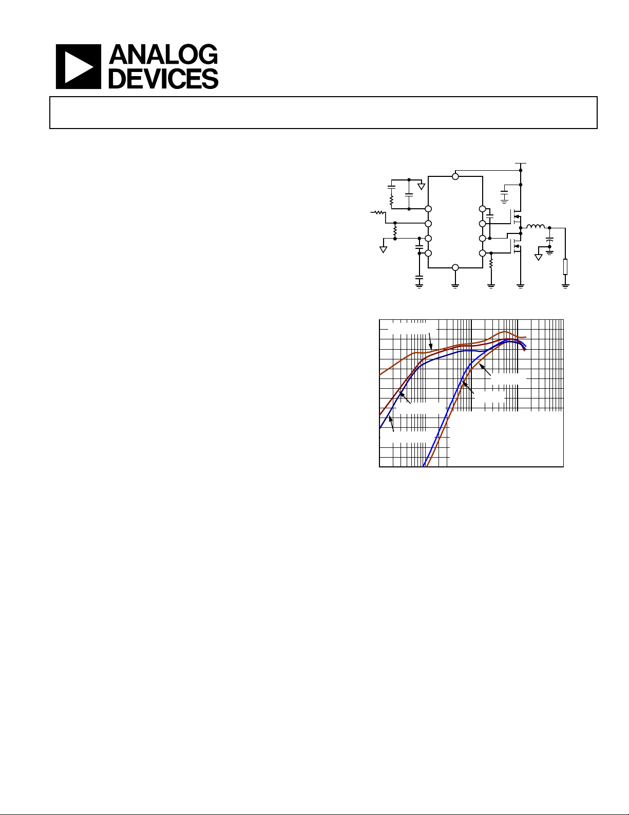
TYPICAL APPLICATIONS CIRCUIT
= 2.95V TO 2 0
IN
C
C
C
C2
R
C
R
TOP
OUT
R
BOT
C
VREG2
C
VREG
100
VIN = 5V (PSM)
95
90
85
80
75
70
65
60
VIN = 13V (PSM)
55
EFFICIENCY (%)
50
45
VIN = 16.5V (PS M )
40
35
30
25
10 100 1k 10k 100k
Figure 2. Efficiency vs. Load Current (V
In addition, an internally fixed soft start period is included to limit
input in-rush current from the input supply during startup and
to provide reverse current protection during soft start for a precharged output. The low-side current-sense, current-gain scheme
and integration of a boost diode, along with the PSM/forced pulsewidth modulation (PWM) option, reduce the external part count
and improve efficiency.
The ADP1870/ADP1871 operate over the −40°C to +125°C
junction temperature range and are available in a 10-lead MSOP
and LFCSP packages.
VIN
ADP1870/
ADP1871
COMP/EN BST
FB DRVH
GND SW
VREG DRVL
PGND
C
BST
R
RES
Figure 1.
VIN = 16.5V
VIN = 13V
TA = 25°C
V
= 1.8V
OUT
f
= 300kHz
SW
WÜRTH INDUCTOR:
744325120, L = 1. 2µH, DCR = 1.8m
INFINEON FETs:
BSC042N03MS G (UPPER/ LOWER)
LOAD CURRENT (mA)
= 1.8 V, 300 kHz)
OUT
C
IN
Q1
L
V
OUT
C
OUT
Q2
LOAD
08730-001
08730-102
Rev. A
Information furnished by Analog Devices is believed to be accurate and reliable. However, no
responsibility is assumed by Analog Devices for its use, nor for any infringements of patents or other
rights of third parties that may result from its use. Specifications subject to change without notice. No
license is granted by implication or otherwise under any patent or patent rights of Analog Devices.
Trademarks and registered trademarks are the property of their respective owners.
One Technology Way, P.O. Box 9106, Norwood, MA 02062-9106, U.S.A.
Tel: 781.329.4700 www.analog.com
Fax: 781.461.3113 ©2010 Analog Devices, Inc. All rights reserved.
Page 2

ADP1870/ADP1871
TABLE OF CONTENTS
Features .............................................................................................. 1
Applications ....................................................................................... 1
General Description ......................................................................... 1
Typical Applications Circuit ............................................................ 1
Revision History ............................................................................... 2
Specifications ..................................................................................... 3
Absolute Maximum Ratings ............................................................ 5
Thermal Resistance ...................................................................... 5
Boundary Condition .................................................................... 5
ESD Caution .................................................................................. 5
Pin Configuration and Function Descriptions ............................. 6
Typical Performance Characteristics ............................................. 7
ADP1870/ADP1871 Block Diagram ............................................ 18
Theory of Operation ...................................................................... 19
Startup .......................................................................................... 19
Soft Start ...................................................................................... 19
Precision Enable Circuitry ........................................................ 19
Undervoltage Lockout ............................................................... 19
On-Board Low Dropout Regulator .......................................... 19
Thermal Shutdown ..................................................................... 20
Programming Resistor (RES) Detect Circuit .......................... 20
Valley Current-Limit Setting .................................................... 20
Hiccup Mode During Short Circuit ......................................... 21
Synchronous Rectifier ................................................................ 22
Power Saving Mode (PSM) Version (ADP1871) ................... 22
Timer Operation ........................................................................ 22
Pseudo-Fixed Frequency ........................................................... 23
Applications Information .............................................................. 24
Feedback Resistor Divider ........................................................ 24
Inductor Selection ...................................................................... 24
Output Ripple Voltage (VRR) .................................................. 24
Output Capacitor Selection ....................................................... 24
Compensation Network ............................................................ 25
Efficiency Considerations ......................................................... 26
Input Capacitor Selection .......................................................... 27
Thermal Considerations ............................................................ 28
Design Example .......................................................................... 29
External Component Recommendations .................................... 31
Layout Considerations ................................................................... 33
IC Section (Left Side of Evaluation Board) ............................. 37
Power Section ............................................................................. 37
Differential Sensing .................................................................... 38
Typical Applications Circuits ........................................................ 39
15 A, 300 kHz High Current Application Circuit .................. 39
5.5 V Input, 600 kHz Application Circuit ............................... 39
300 kHz High Current Application Circuit ............................ 40
Outline Dimensions ....................................................................... 41
Ordering Guide .......................................................................... 42
REVISION HISTORY
6/10—Rev. 0 to Rev. A
Added LFCSP Package ....................................................... Universal
Changes to Applications Section .................................................... 1
Changes to Internal Regulator Characteristics Parameter,
Table 1 ............................................................................................ 3
Changes to Table 2 and Table 3 ....................................................... 5
Changes to Figure 3 and Table 4 ..................................................... 6
Change to Figure 22 ....................................................................... 10
Changes to Figure 65 ...................................................................... 18
Changes to Efficiency Considerations Section ........................... 26
Changes to Table 9 ................................................................................... 28
Added Figure 84; Renumbered Sequentially ...................................... 28
Added Figure 96 ....................................................................................... 41
Changes to Ordering Guide ................................................................... 42
3/10—Revision 0: Initial Version
Rev. A | Page 2 of 44
Page 3

ADP1870/ADP1871
SPECIFICATIONS
All limits at temperature extremes are guaranteed via correlation using standard statistical quality control (SQC). V
− VSW = V
V
BST
REG
− V
RECT_DROP
(see Figure 40 to Figure 42). VIN = 12 V. The specifications are valid for TJ = −40°C to +125°C,
unless otherwise specified.
Table 1.
Parameter Symbol Conditions Min Typ Max Unit
POWER SUPPLY CHARACTERISTICS
High Input Voltage Range VIN C
= 22 µF to PGND (at Pin 1)
IN
ADP1870ARMZ-0.3/ADP1871ARMZ-0.3 (300 kHz) 2.95 12 20 V
ADP1870ARMZ-0.6/ADP1871ARMZ-0.6 (600 kHz) 2.95 12 20 V
ADP1870ARMZ-1.0/ADP1871ARMZ-1.0 (1.0 MHz) 3.25 12 20 V
Quiescent Current I
Shutdown Current
Q_REG
I
REG,SD
I
BST,SD
+ I
VFB = 1.5 V, no switching 1.1 mA
Q_BST
+
COMP/EN < 285 mV 190 280 A
Undervoltage Lockout UVLO Rising VIN (see Figure 35 for temperature variation) 2.65 V
UVLO Hysteresis Falling VIN from operational state 190 mV
INTERNAL REGULATOR
CHARACTERISTICS
VREG Operational Output Voltage V
VREG should not be loaded externally because it is
intended to only bias internal circuitry.
C
REG
VREG
= 1 µF to PGND, 0.22 µF to GND, VIN = 2.95 V to 20 V
ADP1870ARMZ-0.3/ADP1871ARMZ-0.3 (300 kHz) 2.75 5 5.5 V
ADP1870ARMZ-0.6/ADP1871ARMZ-0.6 (600 kHz) 2.75 5 5.5 V
ADP1870ARMZ-1.0/ADP1871ARMZ-1.0 (1.0 MHz) 3.05 5 5.5 V
VREG Output in Regulation VIN = 7 V, 100 mA 4.8 4.981 5.16 V
V
= 12 V, 100 mA 4.8 4.982 5.16 V
IN
Load Regulation 0 mA to 100 mA, VIN = 7 V 32 mV
0 mA to 100 mA, VIN = 20 V 33 mV
Line Regulation VIN = 7 V to 20 V, 20 mA 2.5 mV
V
VIN to V
Dropout Voltage 100 mA out of V
REG
= 7 V to 20 V, 100 mA 2.0 mV
IN
, VIN ≤ 5 V 300 415 mV
REG
Short VREG to PGND VIN = 20 V 229 320 mA
SOFT START
Soft Start Period See Figure 58 3.0 ms
ERROR AMPLIFER
FB Regulation Voltage VFB T
T
T
= +25°C 600 mV
J
= −40°C to +85°C 596 600 604 mV
J
= −40°C to +125°C 594.2 600 605.8 mV
J
Transconductance Gm 320 496 670 µS
FB Input Leakage Current I
V
FB, Leak
= 0.6 V, COMP/EN = released 1 50 nA
FB
CURRENT-SENSE AMPLIFIER GAIN
Programming Resistor (RES)
RES = 47 kΩ ± 1% 2.7 3 3.3 V/V
Value from DRVL to PGND
RES = 22 kΩ ± 1% 5.5 6 6.5 V/V
RES = none 11 12 13 V/V
RES = 100 kΩ ± 1% 22 24 26 V/V
SWITCHING FREQUENCY
ADP1870ARMZ-0.3/
Typical values measured at 50% time points with 0 nF
at DRVH and DRVL; maximum values are guaranteed
by bench evaluation
1
300 kHz
ADP1871ARMZ-0.3 (300 kHz)
On-Time VIN = 5 V, V
= 2 V, TJ = 25°C 1120 1200 1280 ns
OUT
Minimum On-Time VIN = 20 V 146 190 ns
Minimum Off-Time 84% duty cycle (maximum) 340 400 ns
REG
= 5 V,
Rev. A | Page 3 of 44
Page 4

ADP1870/ADP1871
Parameter Symbol Conditions Min Typ Max Unit
ADP1870ARMZ-0.6/
ADP1871ARMZ-0.6 (600 kHz)
On-Time VIN = 5 V, V
Minimum On-Time VIN = 20 V, V
Minimum Off-Time 65% duty cycle (maximum) 340 400 ns
ADP1870ARMZ-1.0/
ADP1871ARMZ-1.0 (1.0 MHz)
On-Time VIN = 5 V, V
Minimum On-Time VIN = 20 V 60 85 ns
Minimum Off-Time 45% duty cycle (maximum) 340 400 ns
OUTPUT DRIVER CHARACTERISTICS
High-Side Driver
Output Source Resistance I
Output Sink Resistance I
Rise Time2 t
Fall Time2 t
Low-Side Driver
Output Source Resistance I
Output Sink Resistance I
Rise Time2 t
Fall Time2 t
Propagation Delays
DRVL Fall to DRVH Rise2 t
DRVH Fall to DRVL Rise2 t
SW Leakage Current I
Integrated Rectifier
Channel Impedance I
PRECISION ENABLE THRESHOLD
Logic High Level VIN = 2.9 V to 20 V, V
Enable Hysteresis VIN = 2.9 V to 20 V, V
COMP VOLTAGE
COMP Clamp Low Voltage V
COMP Clamp High Voltage V
COMP Zero Current Threshold V
THERMAL SHUTDOWN T
Thermal Shutdown Threshold Rising temperature 155 °C
Thermal Shutdown Hysteresis 15 °C
Hiccup Current Limit Timing 6 ms
1
The maximum specified values are with the closed loop measured at 10% to 90% time points (see Figure and Figure 61), C
MOSFETs being Infineon BSC042N03MSG.
2
Not automatic test equipment (ATE) tested.
600 kHz
= 2 V, TJ = 25°C 500 540 580 ns
OUT
= 0.8 V 82 110 ns
OUT
1.0 MHz
= 2 V, TJ = 25°C 285 312 340 ns
OUT
= 1.5 A, 100 ns, positive pulse (0 V to 5 V) 2.25 3 Ω
SOURCE
= 1.5 A, 100 ns, negative pulse (5 V to 0 V) 0.7 1 Ω
SINK
V
r,DR VH
V
f,DRV H
V
r,DR VL
V
f,DRV L
V
tpdhDRVH
V
tpdhDRVL
V
SWLEAK
COMP(l ow)
(2.75 V ≤ V
COMP(h igh)
(2.75 V ≤ V
COMP_ZC T
TMSD
− VSW = 4.4 V, CIN = 4.3 nF (see Figure 60) 25 ns
BST
− VSW = 4.4 V, CIN = 4.3 nF (see Figure 61) 11 ns
BST
= 1.5 A, 100 ns, positive pulse (0 V to 5 V) 1.6 2.2 Ω
SOURCE
= 1.5 A, 100 ns, negative pulse (5 V to 0 V) 0.7 1 Ω
SINK
= 5.0 V, CIN = 4.3 nF (see Figure 61) 18 ns
REG
= 5.0 V, CIN = 4.3 nF (see Figure 60) 16 ns
REG
− VSW = 4.4 V (see Figure 60) 15.4 ns
BST
− VSW = 4.4 V (see Figure 61) 18 ns
BST
= 25 V, VSW = 20 V, V
BST
= 10 mA 22 Ω
SINK
From disabled state, release COMP/EN pin to enable
device (2.75 V ≤ V
REG
≤ 5.5 V) 2.55 V
REG
≤ 5.5 V) 1.07 V
REG
= 5 V 110 µA
REG
= 2.75 V to 5.5 V 245 285 330 mV
REG
= 2.75 V to 5.5 V 37 mV
REG
0.47 V
≤ 5.5 V)
60
= 4.3 nF, and the upper- and lower-side
GATE
Rev. A | Page 4 of 44
Page 5
ADP1870/ADP1871
ABSOLUTE MAXIMUM RATINGS
Table 2.
Parameter Rating
VREG to PGND, GND −0.3 V to +6 V
VIN to PGND −0.3 V to +28 V
FB, COMP/EN to GND −0.3 V to (V
DRVL to PGND −0.3 V to (V
SW to PGND −2.0 V to +28 V
BST to SW −0.6 V to (V
BST to PGND −0.3 V to 28 V
DRVH to SW −0.3 V to V
PGND to GND
θJA (10-Lead MSOP)
2-Layer Board 213.1°C/W
4-Layer Board 171.7°C/W
θJA (10-Lead LFCSP)
4-Layer Board 40°C/W
Operating Junction Temperature
Range
Storage Temperature Range −65°C to +150°C
Soldering Conditions JEDEC J-STD-020
Maximum Soldering Lead
Temperature (10 sec)
±0.3 V
−40°C to +125°C
300°C
Stresses above those listed under Absolute Maximum Ratings
may cause permanent damage to the device. This is a stress
rating only; functional operation of the device at these or any
other conditions above those indicated in the operational
section of this specification is not implied. Exposure to absolute
maximum rating conditions for extended periods may affect
device reliability.
Absolute maximum ratings apply individually only, not in
combination. Unless otherwise specified, all other voltages are
referenced to PGND.
REG
REG
REG
REG
+ 0.3 V)
+ 0.3 V)
+ 0.3 V)
THERMAL RESISTANCE
θJA is specified for the worst-case conditions, that is, a device
soldered in a circuit board for surface-mount packages.
Table 3. Thermal Resistance
Package Type θ
θJA (10-Lead MSOP)
2-Layer Board 213.1 °C/W
4- Layer Board 171.7 °C/W
θJA (10-Lead LFCSP)
4- Layer Board 40 °C/W
1
θJA is specified for the worst-case conditions; that is, θJA is specified for the
device soldered in a circuit board for surface-mount packages.
1
Unit
JA
BOUNDARY CONDITION
In determining the values given in Ta b l e 2 and Ta ble 3 , natural
convection was used to transfer heat to a 4-layer evaluation board.
ESD CAUTION
Rev. A | Page 5 of 44
Page 6
ADP1870/ADP1871
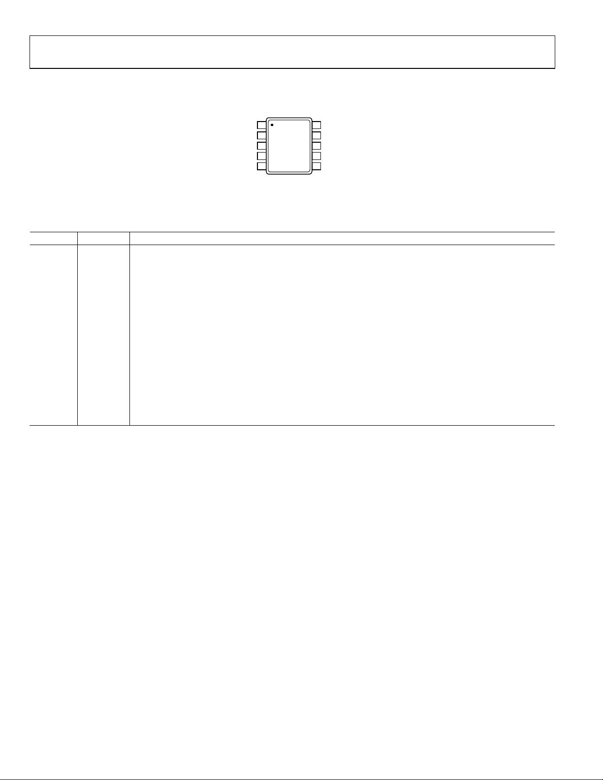
PIN CONFIGURATION AND FUNCTION DESCRIPTIONS
VIN
1
GND
FB
ADP1870/
2
ADP1871
3
TOP VIEW
4
(Not to Scale)
5
COMP/EN
VREG
NOTES
1. THE EXPOSED PAD MUST BE CONNECTED
TO GROUND.
Figure 3. Pin Configuration
Table 4. Pin Function Descriptions
Pin No. Mnemonic Description
1 VIN High Input Voltage. Connect VIN to the drain of the upper-side MOSFET.
2 COMP/EN Output of the Internal Error Amplifier/IC Enable. When this pin functions as EN, applying 0 V to this pin disables the IC.
3 FB Noninverting Input of the Internal Error Amplifier. This is the node where the feedback resistor is connected.
4 GND
Analog Ground Reference Pin of the IC. All sensitive analog components should be connected to this ground
plane (see the Layout Considerations section).
5 VREG
Internal Regulator Supply Bias Voltage for the ADP1870/ADP1871 Controller (Includes the Output Gate Drivers).
A bypass capacitor of 1 µF directly from this pin to PGND and a 0.1 µF across VREG and GND are recommended.
VREG should not be loaded externally because it is intended to only bias internal circuitry.
6 DRVL
Drive Output for the External Lower-Side, N-Channel MOSFET. This pin also serves as the current-sense gain
setting pin (see Figure 69).
7 PGND Power GND. Ground for the lower-side gate driver and lower-side, N-channel MOSFET.
8 DRVH Drive Output for the External Upper-Side, N-Channel MOSFET.
9 SW Switch Node Connection.
10 BST
Bootstrap for the Upper-Side MOSFET Gate Drive Circuitry. An internal boot rectifier (diode) is connected
between VREG and BST. A capacitor from BST to SW is required. An external Schottky diode can also be
connected between VREG and BST for increased gate drive capability.
10
9
8
7
6
BST
SW
DRVH
PGND
DRVL
08730-003
Rev. A | Page 6 of 44
Page 7
ADP1870/ADP1871
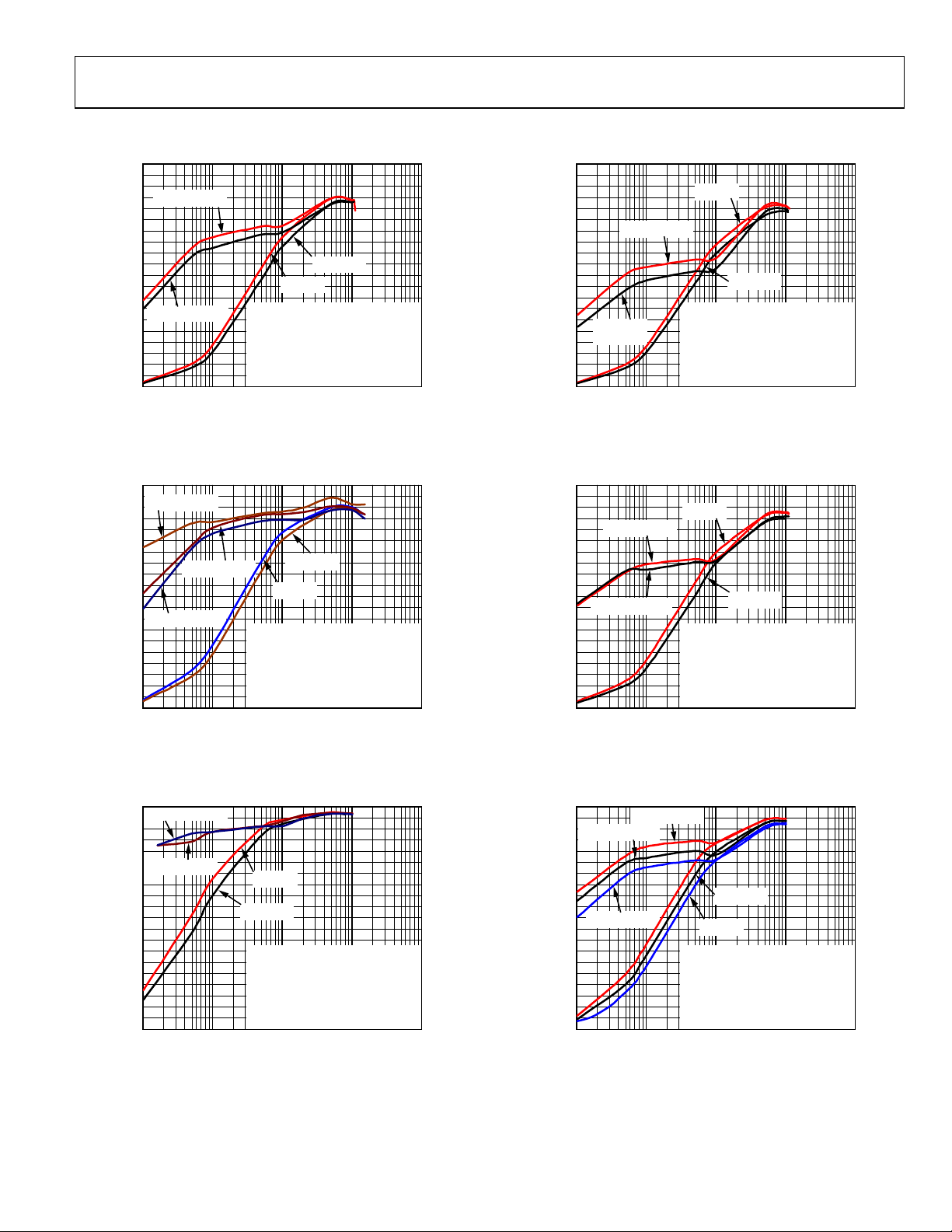
TYPICAL PERFORMANCE CHARACTERISTICS
100
95
90
VIN = 13V (PSM)
85
80
75
70
65
60
55
50
45
40
EFFICIENCY (%)
35
VIN = 16.5V (PS M )
30
25
20
15
10
5
0
10 100 1k 10k 100k
TA = 25°C
V
OUT
f
= 300kHz
SW
WÜRTH INDUCTOR:
744325072, L = 0. 72µH, DCR = 1.3m
INFINEON FETs:
BSC042N03MS G (UPPER/ LOWER)
LOAD CURRENT (mA)
Figure 4. Efficiency—300 kHz, V
VIN = 13V
= 0.8V
VIN = 16.5V
= 0.8 V
OUT
08730-104
100
95
90
85
80
75
70
65
60
55
50
45
40
EFFICIENCY (%)
35
30
25
20
15
10
5
0
10 100 1k 10k 100k
VIN = 13V (PSM)
VIN = 16.5V
(PSM)
Figure 7. Efficiency—600 kHz, V
VIN = 13V
VIN = 16.5V
TA = 25°C
= 0.8V
V
OUT
f
= 600kHz
SW
WÜRTH INDUCTOR:
744355147, L = 0. 47µH, DCR = 0.67m
INFINEON FETs:
BSC042N03MS G (UPPER/ LOWER)
LOAD CURRENT (mA)
= 0.8 V
OUT
08730-107
100
95
VIN = 5V (PSM)
90
85
80
75
70
65
60
55
50
45
40
EFFICIENCY (%)
35
30
25
20
15
10
5
0
VIN = 13V (PSM)
VIN = 16.5V (PS M )
10 100 1k 10k 100k
LOAD CURRENT (mA)
Figure 5. Efficiency—300 kHz, V
100
VIN = 16.5V (PS M )
95
90
85
80
75
VIN = 13V (PSM)
70
65
60
55
50
45
40
EFFICIENCY (%)
35
30
25
20
15
10
5
0
10 100 1k 10k 100k
LOAD CURRENT (mA)
Figure 6. Efficiency—300 kHz, V
VIN = 16.5V
VIN = 13V
TA = 25°C
= 1.8V
V
OUT
f
= 300kHz
SW
WÜRTH INDUCTOR:
744325120, L = 1. 2µH, DCR = 1.8m
INFINEON FETs:
BSC042N03MS G (UPPER/ LOWER)
= 1.8 V
OUT
VIN = 13V
VIN = 16.5V
TA = 25°C
= 7V
V
OUT
f
= 300kHz
SW
WÜRTH INDUCTOR:
7443551200, L = 2.0µH, DCR = 2.6m
INFINEON FETs:
BSC042N03MS G (UPPER/ LOWER)
= 7 V
OUT
100
95
90
85
VIN = 13V (PSM)
80
75
70
65
60
55
50
VIN = 16.5V (PSM)
45
40
EFFICIENCY (%)
35
30
25
20
15
10
5
0
10 100 1k 10k 100k
08730-105
Figure 8. Efficiency—600 kHz, V
100
95
90
VIN = 16.5V (PS M )
85
80
75
70
65
60
55
50
45
40
EFFICIENCY (%)
35
30
25
20
15
10
5
0
10 100 1k 10k 100k
08730-106
VIN = 13V (PSM)
VIN = 20V (PSM)
Figure 9. Efficiency—600 kHz, V
VIN = 13V
VIN = 16.5V
TA = 25°C
= 1.8V
V
OUT
f
= 600kHz
SW
WÜRTH INDUCTOR:
744325072, L = 0. 72µH, DCR = 1.3m
INFINEON FETs:
BSC042N03MS G (UPPER/ LOWER)
LOAD CURRENT (mA)
= 1.8 V
OUT
VIN = 16.5V
VIN = 20V
TA = 25°C
= 5V
V
OUT
f
= 600kHz
SW
WÜRTH INDUCTOR:
744318180, L = 1. 4µH, DCR = 3.2m
INFINEON FETs:
BSC042N03MS G (UPPER/ LOWER)
LOAD CURRENT (mA)
= 5 V
OUT
08730-108
08730-109
Rev. A | Page 7 of 44
Page 8
ADP1870/ADP1871
100
95
90
85
80
75
70
VIN = 13V (PSM)
65
60
55
50
45
40
EFFICIENCY (%)
35
30
VIN = 16.5V (PS M )
25
20
15
10
5
0
10 100 1k 10k 100k
Figure 10. Efficiency—1.0 MHz, V
VIN = 13V
VIN = 16.5V
TA = 25°C
= 0.8V
V
OUT
f
= 1.0MHz
SW
WÜRTH INDUCTOR:
744303012, L = 0. 12µH, DCR = 0.33m
INFINEON FETs:
BSC042N03MS G (UPPER/ LOWER)
LOAD CURRENT (mA)
= 0.8 V
OUT
08730-110
0.807
0.806
0.805
0.804
0.803
0.802
0.801
0.800
0.799
0.798
0.797
OUTPUT VOLTAGE (V)
0.796
0.795
VIN = 13V
0.794
0.793
0.792
+125°C
+25°C
–40°C
0 2000 4000 6000 8000 10,000
VIN = 16.5V
+125°C
+25°C
–40°C
LOAD CURRENT (mA)
Figure 13. Output Voltage Accuracy—300 kHz, V
OUT
08730-013
= 0.8 V
100
95
90
85
80
VIN = 13V (PSM)
75
70
65
60
55
50
45
40
VIN = 16.5V (PSM)
EFFICIENCY (%)
35
30
25
20
15
10
5
0
10 100 1k 10k 100k
Figure 11. Efficiency—1.0 MHz, V
100
95
90
85
VIN = 13V (PSM)
80
75
70
65
60
55
VIN = 16.5V (PS M )
50
45
40
EFFICIENCY (%)
35
30
25
20
15
10
5
0
10 100 1k 10k 100k
Figure 12. Efficiency—1.0 MHz, V
VIN = 13V
VIN = 16.5V
TA = 25°C
= 1.8V
V
OUT
f
= 1.0MHz
SW
WÜRTH INDUCTOR:
744303022, L = 0. 22µH, DCR = 0.33m
INFINEON FETs:
BSC042N03MS G (UPPER/ LOWER)
LOAD CURRENT (mA)
= 1.8 V
OUT
VIN = 13V
VIN = 16.5V
TA = 25°C
= 5V
V
OUT
f
= 1.0MHz
SW
WÜRTH INDUCTOR:
744355090, L = 0. 9µH, DCR = 1.6m
INFINEON FETs:
BSC042N03MS G (UPPER/ LOWER)
LOAD CURRENT (mA)
= 5 V
OUT
1.821
1.816
1.811
1.806
1.801
OUTPUT VOLTAGE (V)
1.796
1.791
1.786
0 1500 3000 4500 6000 7500 9000 10,500 12,000 13,500 15,000
08730-111
VIN = 5.5V
+125°C
+25°C
–40°C
Figure 14. Output Voltage Accuracy—300 kHz, V
7.100
7.095
7.090
7.085
7.080
7.075
7.070
7.065
7.060
7.055
7.050
7.045
7.040
7.035
7.030
OUTPUT VOLTAGE (V)
7.025
7.020
7.015
7.010
7.005
7.000
08730-112
+125°C
+25°C
–40°C
0 1000 2000 3000 4000 5000 6000 7000 8000 9000
Figure 15. Output Voltage Accuracy—300 kHz, V
VIN = 13V
+125°C
+25°C
–40°C
LOAD CURRENT (mA)
VIN = 13V
VIN = 16.5V
LOAD CURRENT (mA)
VIN = 16.5V
+125°C
+25°C
–40°C
OUT
OUT
08730-014
= 1.8 V
08730-015
= 7 V
Rev. A | Page 8 of 44
Page 9
ADP1870/ADP1871
0.808
0.806
0.804
0.802
0.800
0.798
FREQUENCY (kHz)
0.796
0.794
0.792
+125°C
+25°C
–40°C
0 1000 2000 3000 4000 5000 6000 7000 8000 10,0009000
VIN = 13V
VIN = 16.5V
LOAD CURRENT (mA)
Figure 16. Output Voltage Accuracy—600 kHz, V
= 0.8 V
OUT
08730-115
0.807
0.805
0.803
0.801
0.799
0.797
0.795
0.793
OUTPUT VOLTAGE (V)
0.791
0.789
0.787
0 2000 4000 6000 8000 10,000
VIN = 13V
LOAD CURRENT (mA)
+125°C
+25°C
–40°C
VIN = 16.5V
+125°C
+25°C
–40°C
Figure 19. Output Voltage Accuracy—1.0 MHz, V
OUT
= 0.8 V
08730-118
1.818
1.816
1.814
1.812
1.810
1.808
1.806
1.804
1.802
1.800
1.798
1.796
1.794
1.792
1.790
1.788
1.786
1.784
OUTPUT VOLTAGE (V)
1.782
1.780
1.778
1.776
1.774
1.772
1.770
0 12,00010,500900075006000450030001500
VIN = 13V
LOAD CURRENT (mA)
+125°C
+25°C
–40°C
VIN = 16.5V
+125°C
+25°C
–40°C
Figure 17. Output Voltage Accuracy—600 kHz, V
5.030
5.025
5.020
5.015
5.010
5.005
5.000
4.995
4.990
OUTPUT VOLTAGE (V)
4.985
4.980
4.975
4.970
+125°C
+25°C
–40°C
0 1000 2000 3000 4000 5000 6000 7000 8000 9000 10,000
VIN = 13V
VIN = 16.5V
VIN = 20V
LOAD CURRENT (mA)
Figure 18. Output Voltage Accuracy—600 kHz, V
= 1.8 V
OUT
OUT
= 5 V
1.820
1.815
1.810
1.805
1.800
OUTPUT VOLTAGE (V)
1.795
1.790
0
08730-016
VIN = 13V
+125°C
+25°C
–40°C
LOAD CURRENT (mA)
Figure 20. Output Voltage Accuracy—1.0 MHz, V
5.04
5.03
5.02
5.01
5.00
4.99
4.98
4.97
4.96
4.95
OUTPUT VOLTAGE (V)
4.94
4.93
4.92
4.91
4.90
08730-017
VIN = 13V
LOAD CURRENT (mA)
Figure 21. Output Voltage Accuracy—1.0 MHz, V
+125°C
+25°C
–40°C
VIN = 16.5V
+125°C
+25°C
–40°C
VIN = 16.5V
+125°C
+25°C
–40°C
7200640056004800400024001600 32000 960088008000800
OUT
OUT
10,0000 1000 2000 3000 4000 5000 6000 7000 8000 9000
08730-019
= 1.8 V
08730-020
=5 V
Rev. A | Page 9 of 44
Page 10
ADP1870/ADP1871
601.0
600.5
600.0
599.5
599.0
598.5
FEEDBACK VOLTAGE (V)
598.0
597.5
597.0
V
REG
–40.0 –7.5 25.0 57.5 90.0 122.5
= 5V, VIN = 20V
V
REG
= 5V, VIN = 13V
TEMPERATURE (°C)
Figure 22. Feedback Voltage vs. Temperature
08730-121
900
880
860
840
820
800
780
760
SWITCHING FREQUENCY (kHz)
740
720
700
13.0 13.5 14.0 14.5 15.0 15.5 16.0 16.5
+125°C
+25°C
–40°C
VIN (V)
Figure 25. Switching Frequency vs. High Input Voltage, 1.0 MHz,
Range = 13 V to 16.5 V
V
IN
08730-124
325
315
305
295
285
275
SWITCHI NG FREQUENCY (kHz)
265
255
10.8 11.0 11.2 11.4 11.6 11.8 12.0 12.2 12.4 12.6 12.8 13.0 13.2
+125°C
+25°C
–40°C
VIN (V)
NO LOAD
08730-022
Figure 23. Switching Frequency vs. High Input Voltage, 300 kHz, ±10% of 12 V
650
600
550
500
SWITCHI NG FREQUENCY (kHz)
450
400
13.0 13.4 13.8 14.2 14.6 15.0 15.4 15.8 16.2
Figure 24. Switching Frequency vs. High Input Voltage, 600 kHz, V
+125°C
+25°C
–40°C
Range = 13 V to 16.5 V
V
IN
VIN (V)
NO LOAD
= 1.8 V,
OUT
08730-123
280
265
250
235
220
FREQUENCY (kHz)
205
190
VIN = 13V
VIN = 20V
VIN = 16.5V
0 10,0008000600040002000
+125°C
+25°C
–40°C
LOAD CURRENT (mA)
Figure 26. Frequency vs. Load Current, 300 kHz, V
330
320
310
300
290
280
270
FREQUENCY (kHz)
260
250
240
0 15,0012,000 13,50010,500900075006000450030001500
VIN = 20V
VIN = 13V
VIN = 16.5V
+125°C
+25°C
–40°C
LOAD CURRENT (mA)
Figure 27. Frequency vs. Load Current, 300 kHz, V
OUT
OUT
= 0.8 V
= 1.8 V
08730-025
08730-026
Rev. A | Page 10 of 44
Page 11
ADP1870/ADP1871
338
334
330
326
322
318
314
FREQUENCY (kHz)
310
306
302
298
0 6400 7200 8000 8800560048004000320024001600800
VIN = 13V
VIN = 16.5V
+125°C
+25°C
–40°C
LOAD CURRENT (mA)
Figure 28. Frequency vs. Load Current, 300 kHz, V
OUT
08730-027
= 7 V
740
733
726
719
712
705
698
691
684
677
670
663
FREQUENCY (kHz)
656
649
642
635
628
621
0 96008800800072006400560048004000320024001600800
VIN = 13V
VIN = 16.5V
+125°C
+25°C
–40°C
LOAD CURRENT (mA)
Figure 31. Frequency vs. Load Current, 600 kHz, V
OUT
08730-030
= 5 V
540
510
480
450
420
390
FREQUENCY (kHz)
360
330
300
VIN = 13V
VIN = 16.5V
0 12,0001200 2400 3600 4800 6000 7200 8400 9600 10,800
+125°C
+25°C
–40°C
LOAD CURRENT (mA)
Figure 29. Frequency vs. Load Current, 600 kHz, V
675
655
635
615
595
575
555
FREQUENCY (kHz)
535
515
495
VIN = 13V
VIN = 16.5V
0 1000 2000 3000 4000 5000 6000 7000 8000 9000 10,000
LOAD CURRENT (mA)
Figure 30. Frequency vs. Load Current, 600 kHz, V
OUT
OUT
= 0.8 V
+125°C
+25°C
–40°C
= 1.8 V
850
775
700
625
550
FREQUENCY (kHz)
475
400
08730-028
Figure 32. Frequency vs. Load Current, V
1225
1150
1075
1000
925
850
775
FREQUENCY (kHz)
700
625
550
08730-029
Figure 33. Frequency vs. Load Current, 1.0 MHz, V
VIN = 13V
VIN = 16.5V
0 12,00010,0008000600040002000
VIN = 13V +125°C
VIN = 16.5V
0 12,0009600 10,8008400720060004800360024001200
+125°C
+25°C
–40°C
LOAD CURRENT (mA)
+25°C
–40°C
LOAD CURRENT (mA)
= 1.0 MHz, 0.8 V
OUT
= 1.8 V
OUT
08730-031
08730-032
Rev. A | Page 11 of 44
Page 12
ADP1870/ADP1871
FREQUENCY (kHz)
1450
1400
1350
1300
1250
1200
1150
1100
1050
1000
VIN = 13V +125°C
VIN = 16.5V
0 8000800 1600 2400 3200 4000 4800 5600 6400 7200
LOAD CURRENT (mA)
+25°C
–40°C
Figure 34. Frequency vs. Load Current, 1.0 MHz, V
OUT
08730-033
= 5 V
82
80
78
76
74
72
70
68
MAXIMUM DUTY CY CLE (%)
66
64
62
5.5 6.7 7.9 9.1 10.3 11.5 12.7 13.9 15.1 16.3
+125°C
+25°C
–40°C
VIN (V)
Figure 37. Maximum Duty Cycle vs. High Voltage Input (VIN)
08730-036
2.658
2.657
2.656
2.655
2.654
2.653
UVLO (V)
2.652
2.651
2.650
2.649
–40 120100806040200–20
TEMPERATURE ( °C)
Figure 35. UVLO vs. Temperature
95
90
85
80
75
70
65
MAXIMUM DUTY CY CLE (%)
60
55
300 400 500 600 700 800 900 1000
FREQUENCY (kHz)
Figure 36. Maximum Duty Cycle vs. Frequency
+125°C
+25°C
–40°C
680
630
580
530
480
430
380
330
MINUMUM OF F-TIME (ns)
280
230
180
–40 120100806040200–20
08730-034
V
= 2.7V
REG
V
= 3.6V
REG
V
= 5.5V
REG
TEMPERATURE (°C)
08730-037
Figure 38. Minimum Off-Time vs. Temperature
680
630
580
530
480
430
380
330
MINUMUM OFF-TIME (ns)
280
230
180
2.7 5.55.14.74.33.93.53.1
08730-035
Figure 39. Minimum Off-Time vs. V
V
(V)
REG
(Low Input Voltage)
REG
+125°C
+25°C
–40°C
08730-038
Rev. A | Page 12 of 44
Page 13
ADP1870/ADP1871
800
720
640
560
480
400
320
RECTIFI ER DROP (mV)
240
160
80
300 400 500 600 700 800 900 1000
V
= 2.7V
REG
V
= 3.6V
REG
V
= 5.5V
REG
+125°C
+25°C
–40°C
FREQUENCY (kHz)
Figure 40. Internal Rectifier Drop vs. Frequency
08730-039
80
72
64
56
48
40
32
24
BODY DIODE CONDUCT I ON TIME (n s)
16
8
2.73.13.53.94.34.75.15.5
300kHz +125°C
1MHz
V
(V)
REG
+25°C
–40°C
Figure 43. Lower-Side MOSFET Body Diode Conduction Time vs. V
08730-042
REG
1280
1200
1120
1040
960
880
800
720
640
560
480
RECTIFI ER DROP (mV)
400
320
240
160
80
2.73.13.53.94.34.75.15.5
Figure 41. Internal Boost Rectifier Drop vs. V
720
640
560
480
400
VIN = 5.5V
VIN = 13V
VIN = 16.5V
300kHz +125°C
1MHz
Over V
1MHz
300kHz
V
REG
Variation
IN
+25°C
–40°C
(V)
TA = 25°C
(Low Input Voltage)
REG
OUTPUT VOLTAGE
1
2
3
4
CH1 50mV
08730-040
CH3 10V
B
B
W
W
CH2 5A
CH4 5V
INDUCTOR CURRENT
SW NODE
LOW SIDE
M400ns A CH2 3.90A
T 35.8%
08730-043
Figure 44. Power Saving Mode (PSM) Operational Waveform, 100 mA
OUTPUT VOLTAGE
1
INDUCTOR CURRENT
2
320
RECTIFI ER DROP (mV)
240
160
80
2.73.13.53.94.34.75.15.5
Figure 42. Internal Boost Rectifier Drop vs. V
V
(V)
REG
REG
08730-041
Rev. A | Page 13 of 44
3
4
CH1 50mV
CH3 10V
B
B
W
W
CH2 5A
CH4 5V
M4.0µs A CH2 3.90A
T 35.8%
Figure 45. PSM Waveform at Light Load, 500 mA
SW NODE
LOW SIDE
08730-044
Page 14
ADP1870/ADP1871
OUTPUT VOLTAGE
4
INDUCTOR CURRENT
2
OUTPUT VO LTAGE
1
SW NODE
3
CH1 5A
CH3 10V CH4 100mV
M400ns A CH3 2.20V
B
T 30.6%
W
Figure 46. CCM Operation at Heavy Load, 12 A
(See Figure 94 for Application Circuit)
OUTPUT VOLTAGE
2
12A STEP
1
3
4
CH1 10A CH2 200mV
CH3 20V CH4 5V
B
M2ms A CH1 3.40A
W
T 75.6%
Figure 47. Load Transient Step—PSM Enabled, 12 A
(See Figure 94 Application Circuit)
SW NODE
LOW SIDE
1
3
SW NODE
LOW SIDE
12A NEGATIVE STEP
4
CH1 10A CH2 200mV
08730-045
CH3 20V CH4 5V
B
M20µs A CH1 3.40A
W
T 48.2%
08730-048
Figure 49. Negative Step During Heavy Load Transient Behavior—PSM Enabled,
12 A (See Figure 94 Application Circuit)
4
OUTPUT VO LTAGE
12A STEP
1
2
3
CH1 10A CH2 5V
08730-046
CH3 20V CH4 200mV
LOW SIDE
SW NODE
M2ms A CH1 6.20A
B
T 15.6%
W
08730-049
Figure 50. Load Transient Step—Forced PWM at Light Load, 12 A
(See Figure 94 Application Circuit)
2
12A POSITIVE ST EP
OUTPUT VOLTAGE
1
3
SW NODE
LOW SIDE
4
CH1 10A CH2 200mV
CH3 20V CH4 5V
B
M20µs A CH1 3.40A
W
T 30.6%
08730-047
Figure 48. Positiv e Step During Heavy Load Trans ient Behavior—PSM Enabled,
12 A, V
= 1.8 V (See Figure 94 Application Circuit)
OUT
Rev. A | Page 14 of 44
OUTPUT VOLTAGE
4
12A POSITIVE STEP
1
2
3
SW NODE
CH1 10A CH2 5V
CH3 20V CH4 200m V
M20µs A CH1 6.20A
B
T 43.8%
W
LOW SIDE
08730-050
Figure 51. Positive Step During Heavy Load Transient Behavior—Forced PWM
at Light Load, 12 A, V
= 1.8 V (See Figure 94 Application Circuit)
OUT
Page 15

ADP1870/ADP1871
2
OUTPUT VO LTAGE
12A NEGATIVE STEP
1
SW NODE
3
LOW
4
CH1 10A CH2 200mV
CH3 20V CH4 5V
SIDE
B
M10µs A CH1 5.60A
W
T 23.8%
08730-051
Figure 52. Negative Step During Heavy Load Transient Behavior—Forced PWM
at Light Load, 12 A (See Figure 94 Application Circuit)
1
2
4
OUTPUT VOLTAGE
INDUCTOR CURRENT
LOW SIDE
OUTPUT VOLTAGE
1
INDUCTOR CURRENT
2
LOW SIDE
4
SW NODE
3
B
CH1 2V
CH3 10V CH4 5V
CH2 5A
W
M2ms A CH1 720mV
T 32.8%
Figure 55. Start-Up Behavior at Heavy Load, 12 A, 300 kHz
(See Figure 94 Application Circuit)
1
2
4
OUTPUT VOLTAGE
INDUCTOR CURRENT
LOW SIDE
08730-054
SW NODE
3
B
CH1 2V
CH3 10V CH4 5V
CH2 5A
W
M4ms A CH1 920mV
T 49.4%
Figure 53. Output Short-Circuit Behavior Leading to Hiccup Mode
1
OUTPUT VOLTAGE
INDUCTOR CURRENT
2
SW NODE
3
LOW SIDE
4
B
CH1 5V
CH3 10V CH4 5V
CH2 10A
W
M10µs A CH2 8.20A
T 36.2%
Figure 54. Magnified Waveform During Hiccup Mode
SW NODE
3
B
CH1 2V
08730-052
CH3 10V CH4 5V
CH2 5A
W
M4ms A CH1 720mV
T 41.6%
08730-055
Figure 56. Power-Down Waveform During Heavy Load
OUTPUT VOLTAGE
1
INDUCTOR CURRENT
2
SW NODE
3
LOW SIDE
4
B
B
W
W
CH2 5A
CH4 5V
M2µs A CH2 3.90A
T 35.8%
08730-056
CH1 50mV
08730-053
CH3 10V
Figure 57. Output Voltage Ripple Waveform During PSM Operation
at Light Load, 2 A
Rev. A | Page 15 of 44
Page 16

ADP1870/ADP1871
18ns (
t
OUTPUT VO LTAGE
1
LOW SIDE
4
SW NODE
3
INDUCTOR CURRENT
2
B
CH1 1V
CH3 10V
W
B
W
CH2 5A
CH4 2V
M1ms A CH1 1.56V
T 63.2%
Figure 58. Soft Start and RES Detect Waveform
LOW SIDE
TA = 25°C
)
r
,DRVL
4
HIGH SIDE
HS MINUS
SW
3
2
M
TA = 25°C
08730-057
CH3 5V
MATH 2V 20ns
CH2 5V
CH4 2V
24ns (
t
pdh
11ns (
t
f
,DRVH
M20ns A CH2 4.20V
T 39.2%
Figure 61. Upper-Side Driver Falling and Lower-Side Rising Edge Waveforms
= 4.3 nF (Upper-/Lower-Side MOSFET),
(C
IN
Q
= 27 nC (VGS = 4.4 V (Q1), VGS = 5 V (Q3))
TOTAL
570
550
,DRVL
)
LOW SIDE
)
SW NODE
V
V
V
REG
REG
REG
= 5.5V
= 3.6V
= 2.7V
08730-060
4
HIGH SIDE
SW NODE
3
2
M
HS MINUS
SW
CH3 5V
MATH 2V 40ns
CH2 5V
CH4 2V
M40ns A CH2 4.20V
T 29.0%
08730-058
Figure 59. Output Drivers and SW Node Waveforms
HIGH SIDE
t
r
,DRVH
TA = 25°C
)
08730-059
LOW SIDE
4
22ns (
SW NODE
3
2
HS MINUS
M
SW
CH3 5V
MATH 2V 40ns
t
pdh
DRVH
CH2 5V
CH4 2V
16ns (
t
)
f
,DRVL
)
25ns (
M40ns A CH2 4.20V
T 29.0%
Figure 60. Upper-Side Driver Rising and Lower-Side Falling Edge Waveforms
= 4.3 nF (Upper-/Lower-Side MOSFET),
(C
IN
= 27 nC (VGS = 4.4 V (Q1), VGS = 5 V (Q3))
Q
TOTAL
530
510
490
470
TRANSCONDUCTANCE (µS)
450
430
–40 –20 120100806040200
Figure 62. Transconductance (G
680
630
580
530
480
430
TRANSCONDUCTANCE (µS)
380
330
2.7 3.0 5.44.8 5.14.54.23.93.63.3
Figure 63. Transconductance (Gm) vs. V
TEMPERATURE ( °C)
) vs. Temperature
m
V
(V)
REG
REG
+125°C
+25°C
–40°C
08730-061
08730-062
Rev. A | Page 16 of 44
Page 17

ADP1870/ADP1871
1.30
1.25
1.20
1.15
1.10
1.05
1.00
0.95
0.90
0.85
QUIESCENT CURRENT (mA)
0.80
0.75
0.70
2.7 5.55.14.74.3
Figure 64. Quiescent Current vs. V
3.93.53.1
V
+125°C
+25°C
–40°C
REG
(V)
REG
08730-163
Rev. A | Page 17 of 44
Page 18

ADP1870/ADP1871
ADP1870/ADP1871 BLOCK DIAGRAM
VREG
COMP/
EN
FB
I
SS
C
SS
ADP1870/ADP1871
PRECISION
ENABLE BLOCK
REF_ZERO
SS
COMP
SS_REF
ERROR
AMP
0.6V
LOWER
COMP
CLAMP
REF_ZERO
TO ENABLE
ALL BLOCKS
LDO
REF
BIAS BLOCK
AND REFERENCE
PSM
PWM
I
REV
CS
AMP
COMP
CS GAIN SET
t
TIMER
ON
VREG
STATE
MACHINE
TON
BG_REF
PSM
IN_SS
PWM
I
REV
ADC
SW
DH_LO
DRVH
DRVL
DL_LO
INFORMATION
VREG
C
I
R (TRIM M E D)
t
ON
SW FILTER
LEVEL
SHIFT
SW
RES DETECT AND
GAIN SET
0.4V
= 2RC(V
HS
LS
OUT/VIN
VREG
800k
VIN
)
BST
DRVH
300k
SW
8k
DRVL
PGND
GND
08730-063
Figure 65. ADP1870/ADP1871 Block Diagram
Rev. A | Page 18 of 44
Page 19

ADP1870/ADP1871
THEORY OF OPERATION
The ADP1870/ADP1871 are versatile current-mode, synchronous
step-down controllers that provide superior transient response,
optimal stability, and current limit protection by using a constant
on-time, pseudo-fixed frequency with a programmable currentsense gain, current-control scheme. In addition, these devices offer
optimum performance at low duty cycles by utilizing valley
current-mode control architecture. This allows the ADP1870/
ADP1871 to drive all N-channel power stages to regulate output
voltages as low as 0.6 V.
STARTUP
The ADP1870/ADP1871 have an internal regulator (VREG) for
biasing and supplying power for the integrated MOSFET drivers.
A bypass capacitor should be located directly across the VREG
(Pin 5) and PGND (Pin 7) pins. Included in the power-up sequence
is the biasing of the current-sense amplifier, the current-sense
gain circuit (see the Programming Resistor (RES) Detect Circuit
section), the soft start circuit, and the error amplifier.
The current-sense blocks provide valley current information
(see the Programming Resistor (RES) Detect Circuit section)
and are a variable of the compensation equation for loop stability
(see the Compensation Network section). The valley current
information is extracted by forcing 0.4 V across the DRVL output
and PGND pin, which generates a current depending on the
resistor across DRVL and PGND in a process performed by the
RES detect circuit. The current through the resistor is used to set
the current-sense amplifier gain. This process takes approximately
800 µs, after which the drive signal pulses appear at the DRVL
and DRVH pins synchronously and the output voltage begins to
rise in a controlled manner through the soft start sequence.
The rise time of the output voltage is determined by the soft
start and error amplifier blocks (see the Soft Start section). At
the beginning of a soft start, the error amplifier charges the
external compensation capacitor, causing the COMP/EN pin to
rise above the enable threshold of 285 mV, thus enabling the
ADP1870/ADP1871.
SOFT START
The ADP1870/ADP1871 have digital soft start circuitry, which
involves a counter that initiates an incremental increase in current,
by 1 µA, via a current source on every cycle through a fixed internal
capacitor. The output tracks the ramping voltage by producing
PWM output pulses to the upper-side MOSFET. The purpose is to
limit the in-rush current from the high voltage input supply (V
to the output (V
OUT
).
)
IN
PRECISION ENABLE CIRCUITRY
The ADP1870/ADP1871 employ precision enable circuitry. The
enable threshold is 285 mV typical with 35 mV of hysteresis.
The devices are enabled when the COMP/EN pin is released,
allowing the error amplifier output to rise above the enable
threshold (see Figure 66). Grounding this pin disables the
ADP1870/ADP1871, reducing the supply current of the devices
to approximately 140 µA. For more information, see Figure 67.
ADP1870/ADP1871
FB
VREG
SS
ERROR
COMP/EN
C
C
C
C2
R
C
Figure 66. Release COMP/EN Pin to Enable the ADP1870/ADP1871
COMP/EN
>2.4V
2.4V
1.0V
500mV
285mV
0V
Figure 67. COMP/EN Voltage Range
AMPLIFIER
PRECISION
ENABLE
285mV
HICCUP MODE INITIALIZED
MAXIMUM CURRENT (UPPER CLAMP)
ZERO CURRENT
USABLE RANGE ONLY AFTER SO F T S TAR T
PERIOD IF CONTUNUOUS CONDUCTION
MODE OF OPERATI ON IS SELE CTE D.
LOWER CLAM P
PRECISION ENABLE THRESHOLD
35mV HYSTERESIS
0.6V
TO ENABLE
ALL BLOCKS
08730-064
08730-065
UNDERVOLTAGE LOCKOUT
The undervoltage lockout (UVLO) feature prevents the part from
operating both the upper- and lower-side MOSFETs at extremely
low or undefined input voltage (V
) ranges. Operation at an
IN
undefined bias voltage may result in the incorrect propagation
of signals to the high-side power switches. This, in turn, results
in invalid output behavior that can cause damage to the output
devices, ultimately destroying the device tied to the output. The
UVLO level has been set at 2.65 V (nominal).
ON-BOARD LOW DROPOUT REGULATOR
The ADP1870 uses an on-board LDO to bias the internal digital
and analog circuitry. With proper bypass capacitors connected
to the VREG pin (output of internal LDO), this pin also provides
power for the internal MOSFET drivers. It is recommended to
float VREG if VIN is utilized for greater than 5.5 V operation.
The minimum voltage where bias is guaranteed to operate is
2.75 V at VREG.
For applications where VIN is decoupled from VREG, the
minimum voltage at VIN must be 2.9 V. It is recommended that
Rev. A | Page 19 of 44
Page 20

ADP1870/ADP1871
VIN and VREG be tied together if the VIN pin is subjected to a
2.75 V rail.
Table 5. Power Input and LDO Output Configurations
VIN VREG Comments
>5.5 V Float Must use the LDO
<5.5 V Connect to VIN
LDO drop voltage is not
= 2.75 V)
REG
=
IN
realized (that is, if V
2.75 V, then V
<5.5 V Float LDO drop is realized
Ranges above
and below 5.5 V
Float
LDO drop is realized,
minimum V
recom-
IN
mendation is 2.95 V
THERMAL SHUTDOWN
The thermal shutdown is a self-protection feature to prevent the
IC from damage due to a very high operating junction temperature.
If the junction temperature of the device exceeds 155°C, the part
enters the thermal shutdown state. In this state, the device shuts off
both the upper- and lower-side MOSFETs and disables the entire
controller immediately, thus reducing the power consumption of
the IC. The part resumes operation after the junction temperature
of the part cools to less than 140°C.
PROGRAMMING RESISTOR (RES) DETECT CIRCUIT
Upon startup, one of the first blocks to become active is the RES
detect circuit. This block powers up before soft start begins. It
forces a 0.4 V reference value at the DRVL output (see Figure 68)
and is programmed to identify four possible resistor values: 47 kΩ,
22 kΩ, open, and 100 kΩ.
The RES detect circuit digitizes the value of the resistor at the
DRVL pin (Pin 6). An internal ADC outputs a 2-bit digital code
that is used to program four separate gain configurations in the
current-sense amplifier (see Figure 69). Each configuration corresponds to a current-sense gain (A
24 V/V, respectively (see Ta bl e 6 and Ta b le 7 ). This variable is used
for the valley current-limit setting, which sets up the appropriate
current-sense gain for a given application and sets the compensation
necessary to achieve loop stability (see the Valley Current-Limit
Setting and Compensation Network sections).
ADP1870/
ADP1871
DRVH
DRVL
CS GAIN
PROGRAMMING
Figure 68. Programming Resistor Location
) of 3 V/V, 6 V/V, 12 V/V,
CS
Q1
SW
Q2
R
RES
08730-066
CS
AMP
RES
ADC
0.4V
CS GAIN SET
DRVL
Figure 69. RES Detect Circuit for Current-Sense Gain Programming
Table 6. Current-Sense Gain Programming
Resistor ACS
47 kΩ 3 V/V
22 kΩ 6 V/V
Open 12 V/V
100 kΩ 24 V/V
VALLEY CURRENT-LIMIT SETTING
The architecture of the ADP1870/ADP1871 is based on valley
current-mode control. The current limit is determined by three
components: the R
fier output voltage swing (COMP), and the current-sense gain.
The COMP range is internally fixed at 1.4 V. The current-sense
gain is programmable via an external resistor at the DRVL pin (see
the Programming Resistor (RES) Detect Circuit section). The
R
of the lower-side MOSFET can vary over temperature and
ON
usually has a positive T
ture); therefore, it is recommended to program the current-sense
gain resistor based on the rated R
Because the ADP1870/ADP1871 are based on valley current
control, the relationship between I
where:
K
is the ratio between the inductor ripple current and the
I
desired average load current (see Figure 70).
I
is the desired valley current limit.
CLIM
I
is the current load.
LOAD
Establishing K
Inductor Selection section), but in most cases K
LOAD CURRENT
of the lower-side MOSFET, the error ampli-
ON
(meaning that it increases with tempera-
C
of the MOSFET at 125°C.
ON
and I
CLIM
K
⎞
⎛
II
LOADCLIM
helps to determine the inductor value (see the
I
I
−×=
1
⎜
2
⎝
RIPPLE CURRENT =
⎟
⎠
SW
PGND
is as follows:
LOAD
= 0.33.
I
I
LOAD
3
08730-067
Rev. A | Page 20 of 44
VALLEY CURRENT L I M I T
Figure 70. Valley Current Limit to Average Current Relation
8730-068
Page 21

ADP1870/ADP1871
A
When the desired valley current limit (I
the current-sense gain can be calculated as follows:
V4.1
CLIM
=
RAI×
ONCS
where:
R
is the channel impedance of the lower-side MOSFET.
ON
is the current-sense gain multiplier (see Tab le 6 and Ta b l e 7 ).
A
CS
Although the ADP1870/ADP1871 have only four discrete currentsense gain settings for a given R
variable, Tab le 7 and Figure 71
ON
outline several available options for the valley current setpoint
based on various R
values.
ON
Table 7. Valley Current Limit Program1
Valley Current Level
RON
(mΩ)
1.5 38.9
2 29.2
2.5 23.3
3 39.0 19.5
3.5 33.4 16.7
4.5 26.0 13
5 23.4 11.7
5.5 21.25 10.6
10 23.3 11.7 5.83
15 31.0 15.5 7.75 7.5
18 26.0 13.0 6.5 3.25
1
47 kΩ 22 kΩ Open 100 kΩ
ACS = 3 V/V ACS = 6 V/V ACS = 12 V/V ACS = 24 V/V
Refer to Figure 71 for more information and a graphical representation.
39
37
35
33
31
29
27
25
23
21
19
17
15
13
VALLEY CURRENT L IMIT (A)
11
RES = 100k
9
= 24V/V
A
7
CS
5
3
1234567891011121314151617181920
RES = NO RES
= 12V/V
A
CS
RON (m)
Figure 71. Valley Current-Limit Value vs. R
for Each Programming Resistor (RES)
) has been determined,
CLIM
RES = 47k
= 3V/V
A
CS
RES = 22k
= 6V/V
A
CS
of the Lower-Side MOSFET
ON
REPEATED CURRENT-L I M I T
VIOLAT ION DETECTE D
HS
CLIM
The valley current limit is programmed as outlined in Table 7
and Figure 71. The inductor chosen must be rated to handle the
peak current, which is equal to the valley current from Tab le 7
plus the peak-to-peak inductor ripple current (see the Inductor
Selection section). In addition, the peak current value must be
used to compute the worst-case power dissipation in the
MOSFETs (see Figure 72).
INDUCTOR
CURRENT
Figu re 72. Valley Current-Limit Threshold in Relation to Inductor Ripple Current
HICCUP MODE DURING SHORT CIRCUIT
A current-limit violation occurs when the current across the
source and drain of the lower-side MOSFET exceeds the
current-limit setpoint. When 32 current-limit violations are
detected, the controller enters idle mode and turns off the
MOSFETs for 6 ms, allowing the converter to cool down. Then,
the controller reestablishes soft start and begins to cause the
output to ramp up again (see Figure 73). While the output
ramps up, COMP is monitored to determine if the violation is
still present. If it is still present, the idle event occurs again,
followed by the full-chip power-down sequence. This cycle
continues until the violation no longer exists. If the violation
disappears, the converter is allowed to switch normally,
maintaining regulation.
08730-069
A PREDETERMINED NUM BE R
OF PULSES IS COUNTED TO
ALLOW T HE CONVERTER
TO COOL DOWN
MAXIMUM DC LOAD
35A
I = 45%
I = 33%
OF 30A
VALLEY CURRENT - LIMIT
THRESHOLD (SET FOR 25A)
OF 32.25A
30A
SOFT START IS
REINITIALIZED TO
MONITO R IF THE
VIOLATION
STILL EXISTS
CURRENT
39.5A
32.25A
I = 65%
OF 37A
49
COMP
37A
OUTPUT
2.4V
COMP
OUTPUT
SWING
1V0A
08730-070
ZERO
CURRENT
Figure 73. Idle Mode Entry Sequence Due to Current-Limit Violation
08730-071
Rev. A | Page 21 of 44
Page 22

ADP1870/ADP1871
SYNCHRONOUS RECTIFIER
The ADP1870/ADP1871 employ an internal lower-side MOSFET
driver to drive the external upper- and lower-side MOSFETs.
The synchronous rectifier not only improves overall conduction
efficiency, but also ensures proper charging to the bootstrap
capacitor located at the upper-side driver input. This is beneficial
during startup to provide sufficient drive signal to the external
upper-side MOSFET and to attain fast turn-on response, which is
essential for minimizing switching losses. The integrated upperand lower-side MOSFET drivers operate in complementary
fashion with built-in anticross conduction circuitry to prevent
unwanted shoot-through current that may potentially damage the
MOSFETs or reduce efficiency as a result of excessive power loss.
POWER SAVING MODE (PSM) VERSION (ADP1871)
The power saving mode version of the ADP1870 is the ADP1871.
The ADP1871 operates in the discontinuous conduction mode
(DCM) and pulse skips at light load to mid load currents. It
outputs pulses as necessary to maintain output regulation. Unlike
the continuous conduction mode (CCM), DCM operation
prevents negative current, thus allowing improved system
efficiency at light loads. Current in the reverse direction through
this pathway, however, results in power dissipation and therefore
a decrease in efficiency.
HS
t
ON
HS AND LS ARE OFF
OR IN IDLE MODE
AS THE INDUCTOR
CURRENT APPROACHES
ZERO CURRENT, THE STATE
MACHINE TURNS OFF THE
LOWER-SIDE MOSFET.
SW
10mV
I
Q2
I
LOAD
LS
0A
t
OFF
Figure 74. Discontinuous Mode of Operation (DCM)
To minimize the chance of negative inductor current buildup,
an on-board zero-cross comparator turns off all upper- and
lower-side switching activities when the inductor current
approaches the zero current line, causing the system to enter
idle mode, where the upper- and lower-side MOSFETs are
turned off. To ensure idle mode entry, a 10 mV offset, connected
in series at the SW node, is implemented (see Figure 75).
ZERO-CROSS
COMPARATOR
08730-072
As soon as the forward current through the lower-side
MOSFET decreases to a level where
10 mV = I
the zero-cross comparator (or I
Q2
× R
ON(Q2)
comparator) emits a signal to
REV
turn off the lower-side MOSFET. From this point, the slope of the
inductor current ramping down becomes steeper (see Figure 76)
as the body diode of the lower-side MOSFET begins to conduct
current and continues conducting current until the remaining
energy stored in the inductor has been depleted.
ANOTHER
TRIGGERE D WHEN V
FALLS BELOW REGULATION
SW
LS
I
LOAD
0A
Figure 76. 10 mV Offset to Ensure Prevention of Negative Inductor Current
t
EDGE IS
ON
OUT
HS AND LS
IN IDLE MODE
ZERO-CROSS COMPARATOR
DETECTS 10mV OFFSET AND
TURNS OFF L S
10mV = R
× I
ON
LOAD
t
ON
08730-074
The system remains in idle mode until the output voltage drops
below regulation. A PWM pulse is then produced, turning on the
upper-side MOSFET to maintain system regulation. The
ADP1871 does not have an internal clock, so it switches purely
as a hysteretic controller as described in this section.
TIMER OPERATION
The ADP1870/ADP1871 employ a constant on-time architecture,
which provides a variety of benefits, including improved load
and line transient response when compared with a constant
(fixed) frequency current-mode control loop of comparable
loop design. The constant on-time timer, or t
the high input voltage (V
) and the output voltage (V
IN
SW waveform information to produce an adjustable one-shot
PWM pulse that varies the on-time of the upper-side MOSFET in
response to dynamic changes in input voltage, output voltage, and
load current conditions to maintain regulation. It then generates
an on-time (t
ON
) pulse that is inversely proportional to V
ON
V
OUT
Kt ×=
V
IN
where:
K is a constant that is trimmed using an RC timer product for
the 300 kHz, 600 kHz, and 1.0 MHz frequency options.
timer, senses
ON
OUT
) using
IN.
LS
Q2
08730-073
Figure 75. Zero-Cross Comparator with 10 mV of Offset
Rev. A | Page 22 of 44
Page 23

ADP1870/ADP1871
K
t
ON
INFORMATION
Figure 77. Constant On-Time Time
VREG
C
I
SW
R (TRIMMED)
V
IN
08730-075
The constant on-time (tON) is not strictly “constant” because it
varies with V
and V
IN
. However, this variation occurs in such
OUT
a way as to keep the switching frequency virtually independent
and V
of V
IN
The t
timer uses a feedforward technique, applied to the constant
ON
OUT
.
on-time control loop, making it a pseudo-fixed frequency to a first
order. Second-order effects, such as dc losses in the external power
MOSFETs (see the Efficiency Consideration section), cause some
variation in frequency vs. load current and line voltage. These
effects are shown in Figure 23 to Figure 34. The variations in
frequency are much reduced compared with the variations
generated when the feedforward technique is not utilized.
The feedforward technique establishes the following relationship:
1
=
is the controller switching frequency (300 kHz,
SW
where f
f
SW
600 kHz, and 1.0 MHz).
timer senses VIN and V
The t
ON
to minimize frequency
OUT
variation as previously explained. This provides a pseudo-fixed
frequency as explained in the Pseudo-Fixed Frequency section.
To allow headroom for V
and V
IN
sensing, adhere to the
OUT
following equations:
≥ VIN/8 + 1.5
V
REG
V
≥ V
OUT
/4
is 5 V, these equations are
REG
inputs, care may be
REG
REG
For typical applications where V
not relevant; however, for lower V
required.
To illustrate this feature more clearly, this section describes
one such load transient event—a positive load step—in detail.
During load transient events, the high-side driver output pulse
width stays relatively consistent from cycle to cycle; however,
the off-time (DRVL on-time) dynamically adjusts according to
the instantaneous changes in the external conditions mentioned.
When a positive load step occurs, the error amplifier (out of phase
of the output, V
) produces new voltage information at its output
OUT
(COMP). In addition, the current-sense amplifier senses new
inductor current information during this positive load transient
event. The error amplifier’s output voltage reaction is compared
with the new inductor current information that sets the start of
the next switching cycle. Because current information is produced
from valley current sensing, it is sensed at the down ramp of the
inductor current, whereas the voltage loop information is sensed
through the counter action upswing of the error amplifier’s
output (COMP).
The result is a convergence of these two signals (see Figure 78),
which allows an instantaneous increase in switching frequency
during the positive load transient event. In summary, a positive
load step causes V
to transient down, which causes COMP to
OUT
transient up and therefore shortens the off-time. This resulting
increase in frequency during a positive load transient helps to
quickly bring V
back up in value and within the regulation
OUT
window.
Similarly, a negative load step causes the off-time to lengthen in
response to V
demagnetizing phase, helping to bring V
rising. This effectively increases the inductor
OUT
within regulation.
OUT
In this case, the switching frequency decreases, or experiences a
foldback, to help facilitate output voltage recovery.
Because the ADP1870/ADP1871 has the ability to respond rapidly
to sudden changes in load demand, the recovery period in which
the output voltage settles back to its original steady state operating
point is much quicker than it would be for a fixed-frequency
equivalent. Therefore, using a pseudo-fixed frequency results in
significantly better load transient performance than using a
fixed frequency.
PSEUDO-FIXED FREQUENCY
The ADP1870/ADP1871 employ a constant on-time control
scheme. During steady state operation, the switching frequency
stays relatively constant, or pseudo-fixed. This is due to the one-
timer that produces a high-side PWM pulse with a
shot t
ON
“fixed” duration, given that external conditions such as input
voltage, output voltage, and load current are also at steady state.
During load transients, the frequency momentarily changes for
the duration of the transient event so that the output comes
PWM OUTPUT
back within regulation more quickly than if the frequency were
fixed or if it were to remain unchanged. After the transient
event is complete, the frequency returns to a pseudo-fixed
frequency value to a first order.
Rev. A | Page 23 of 44
LOAD CURRENT
DEMAND
CS AMP
OUTPUT
ERROR AMP
OUTPUT
f
SW
Figure 78. Load Transient Response Operation
>
f
SW
VALLEY
TRIP POINTS
08730-076
Page 24

ADP1870/ADP1871
I
×=Δ
Δ
APPLICATIONS INFORMATION
FEEDBACK RESISTOR DIVIDER
The required resistor divider network can be determined for a
given V
is fixed at 0.6 V. Selecting values for R
value because the internal band gap reference (V
OUT
and RB determines the
T
REF
minimum output load current of the converter. Therefore, for a
given value of R
, the RT value can be determined through the
B
following expression:
V
OUT
×=
RR
B
T
V)6.0( −
V6.0
INDUCTOR SELECTION
The inductor value is inversely proportional to the inductor
ripple current. The peak-to-peak ripple current is given by
LOAD
IKI ≈×=Δ
IL
LOAD
where K
is typically 0.33.
I
The equation for the inductor value is given by
VV
−
IN
L ×
=
L
)(
OUT
fI
×Δ
SW
where:
is the high voltage input.
V
IN
is the desired output voltage.
V
OUT
f
is the controller switching frequency (300 kHz, 600 kHz, and
SW
1.0 MHz).
When selecting the inductor, choose an inductor saturation
rating that is above the peak current level, and then calculate
the inductor current ripple (see the Valley Current-Limit
Setting section and Figure 79).
52
50
48
46
44
42
40
38
36
34
32
30
28
26
24
22
20
18
PEAK INDUCTOR CURRENT (A)
16
14
12
10
8
6 8 10 12 14 16 18 20 22 24 26 28 30
Figure 79. Peak Inductor Current vs. Valley Current Limit for 33%, 40%, and
VALLEY CURRENT LIMIT ( A)
50% of Inductor Ripple Current
3
V
OUT
V
IN
I = 50%
I = 40%
I = 33%
08730-077
)
Table 8. Recommended Inductors
L
DCR
I
Dimensions
(μH)
(mΩ)
0.12 0.33 55 10.2 × 7 Würth Elek. 744303012
0.22 0.33 30 10.2 × 7 Würth Elek. 744303022
0.47 0.67 50 13.2 × 12.8 Würth Elek. 744355147
0.72 1.3 35 10.5 × 10.2 Würth Elek. 744325072
0.9 1.6 28 13 × 12.8 Würth Elek. 744355090
1.2 1.8 25 10.5 × 10.2 Würth Elek. 744325120
1.0 3.3 20 10.5 × 10.2 Würth Elek. 7443552100
1.4 3.2 24 14 × 12.8 Würth Elek. 744318180
2.0 2.6 22 13.2 × 12.8 Würth Elek. 7443551200
0.8 2.5 16.5 12.5 × 12.5 AIC Technology CEP125U-R80
SAT
(A)
(mm)
Manufacturer
Model
Number
OUTPUT RIPPLE VOLTAGE (ΔVRR)
The output ripple voltage is the ac component of the dc output
voltage during steady state. For a ripple error of 1.0%, the
output capacitor value needed to achieve this tolerance can be
determined using the following equation. (Note that an
accuracy of 1.0% is possible only during steady state conditions,
not during load transients.)
VV
)01.0(
RR
OUT
OUTPUT CAPACITOR SELECTION
The primary objective of the output capacitor is to facilitate the
reduction of the output voltage ripple; however, the output
capacitor also assists in the output voltage recovery during load
transient events. For a given load current step, the output
voltage ripple generated during this step event is inversely
proportional to the value chosen for the output capacitor. The
speed at which the output voltage settles during this recovery
period depends on where the crossover frequency (loop
bandwidth) is set. This crossover frequency is determined by
the output capacitor, the equivalent series resistance (ESR) of
the capacitor, and the compensation network.
To calculate the small-signal voltage ripple (output ripple
voltage) at the steady state operating point, use the following
equation:
OUT
⎛
⎜
IC
×Δ=
L
⎜
SW
⎝
1
[]
LRIPPLE
where ESR is the equivalent series resistance of the output
capacitors.
To calculate the output load step, use the following equation:
I
×=
2
C
OUT
where V
is the amount that V
DROOP
a given positive load current step (I
LOAD
ESRIVf
×Δ−Δ×
LOADDROOPSW
is allowed to deviate for
OUT
).
LOAD
⎞
⎟
⎟
)(8
ESRIVf
×Δ−Δ××
⎠
))((
Rev. A | Page 24 of 44
Page 25

ADP1870/ADP1871
Ceramic capacitors are known to have low ESR. However, the
trade-off of using X5R technology is that up to 80% of its capacitance might be lost due to derating as the voltage applied across
the capacitor is increased (see Figure 80). Although X7R series
capacitors can also be used, the available selection is limited to
only up to 22 µF.
20
10
0
–10
–20
–30
–40
–50
–60
–70
CAPACITANCE CHARGE ( %)
–80
10µF TDK 25V, X7R, 1210 C3225X7R1E106M
22µF MURATA 25V , X7R, 1210 GRM 32E R71E226KE15L
–90
47µF MURATA 16V, X5R, 1210 G RM 32E R61C47 6KE 15L
–100
0 5 10 15 20 25 30
Figure 80. Capacitance vs. DC Voltage Characteristics for Ceramic Capacitors
X5R (16V)
X7R (50V)
X5R (25V)
DC VOLTAGE (VDC)
08730-078
Electrolytic capacitors satisfy the bulk capacitance requirements
for most high current applications. Because the ESR of electrolytic
capacitors is much higher than that of ceramic capacitors, when
using electrolytic capacitors, several MLCCs should be mounted
in parallel to reduce the overall series resistance.
COMPENSATION NETWORK
Due to their current-mode architecture, the ADP1870/ADP1871
require Type II compensation. To determine the component
values needed for compensation (resistance and capacitance
values), it is necessary to examine the converter’s overall loop
gain (H) at the unity gain frequency (f
V
GGH ××××== V/V1
M
OUT
CS
V
REF
Examining each variable at high frequency enables the unitygain transfer function to be simplified to provide expressions
for the R
COMP
and C
Output Filter Impedance (Z
component values.
COMP
FILT
Examining the filter’s transfer function at high frequencies
simplifies to
1
Z
FILTER
=
sC
OUT
at the crossover frequency (s = 2πf
/10) when H = 1 V/V:
SW
ZZ
COMP
)
).
CROSS
FILT
Error Amplifier Output Impedance (Z
Assuming that CC2 is significantly smaller than C
COMP
)
, CC2 can
COMP
be omitted from the output impedance equation of the error
amplifier. The transfer function simplifies to
ffR
Z
COMP
=
CROSSCOMP
f
CROSS
ZERO
)( +
and
1
ff ×=
SWCROSS
12
f
where
, the zero frequency, is set to be 1/4th of the crossover
ZERO
frequency for the ADP1870.
Error Amplifier Gain (GM)
The error amplifier gain (transconductance) is
G
= 500 µA/V
M
Current-Sense Loop Gain (GCS)
The current-sense loop gain is
1
=
CS
(A/V)
RAG×
ONCS
where:
A
(V/V) is programmable for 3 V/V, 6 V/V, 12 V/V, and 24 V/V
CS
(see the Programming Resistor (RES) Detect Circuit and Val l e y
Current-Limit Setting sections).
R
is the channel impedance of the lower-side MOSFET.
ON
Crossover Frequency
The crossover frequency is the frequency at which the overall
loop (system) gain is 0 dB (H = 1 V/V). For current-mode
converters, such as the ADP1870, it is recommended that the
user set the crossover frequency between 1/10
th
and 1/15th of the
switching frequency.
1
ff
=
SWCROSS
12
The relationship between C
COMP
and f
(zero frequency) is as
ZERO
follows:
ZERO
1
The zero frequency is set to 1/4
)
CRf××π=2
COMPCOMP
th
of the crossover frequency.
Combining all of the above parameters results in
2
R
C
COMP
COMP
f
CROSS
=
=
CROSS
2
+
ff
ZERO
1
COMP
π
CROSS
×
fR
××π×
ZERO
GG
M
V
Cf
CS
OUT
OUT
×
V
REF
Rev. A | Page 25 of 44
Page 26

ADP1870/ADP1871
[
]
(
)
[
]
×××××=
EFFICIENCY CONSIDERATIONS
One of the important criteria to consider in constructing a dc-to-dc
converter is efficiency. By definition, efficiency is the ratio of the
output power to the input power. For high power applications at
load currents up to 20 A, the following are important MOSFET
parameters that aid in the selection process:
• V
• R
• Q
• C
• C
The following are the losses experienced through the external
component during normal switching operation:
• Channel conduction loss (both of the MOSFETs)
• MOSFET driver loss
• MOSFET switching loss
• Body diode conduction loss (lower-side MOSFET)
• Inductor loss (copper and core loss)
Channel Conduction Loss
During normal operation, the bulk of the loss in efficiency is due
to the power dissipated through MOSFET channel conduction.
Power loss through the upper-side MOSFET is directly proportional to the duty cycle (D) for each switching period, and
the power loss through the lower-side MOSFET is directly
proportional to 1 − D for each switching period. The selection
of MOSFETs is governed by the amount of maximum dc load
current that the converter is expected to deliver. In particular,
the selection of the lower-side MOSFET is dictated by the
maximum load current because a typical high current application
employs duty cycles of less than 50%. Therefore, the lower-side
MOSFET is in the on state for most of the switching period.
MOSFET Driver Loss
Other dissipative elements are the MOSFET drivers. The contributing factors are the dc current flowing through the driver
during operation and the Q
: the MOSFET threshold voltage applied between
GS (TH)
the gate and the source
: the MOSFET on resistance during channel
DS (ON)
conduction
: the total gate charge
G
: the input capacitance of the upper-side switch
N1
: the input capacitance of the lower-side switch
N2
()
1
parameter of the external MOSFETs.
GATE
N2(ON)N1(ON)N1,N2(CL)
IRDRDP ××−+×=
2
LOAD
800
720
640
560
480
400
320
RECTIFI ER DROP (mV)
240
160
80
300 1000900800700600500400
Figure 81. Internal Rectifier Voltage Drop vs. Switching Frequency
V
= 2.7V
REG
V
= 3.6V
REG
V
= 5.5V
REG
SWITCHI NG FREQUENCY (kHz)
+125°C
+25°C
–40°C
08730-079
Switching Loss
The SW node transitions due to the switching activities of the
upper- and lower-side MOSFETs. This causes removal and
replenishing of charge to and from the gate oxide layer of the
MOSFET, as well as to and from the parasitic capacitance
associated with the gate oxide edge overlap and the drain and
source terminals. The current that enters and exits these charge
paths presents additional loss during these transition times. This
loss can be approximately quantified by using the following
equation, which represents the time in which charge enters and
exits these capacitive regions:
t
SW-TRANS
= R
GATE
× C
TOTAL
where:
C
is the C
TOTAL
R
is the gate input resistance of the external MOSFET.
GATE
+ CGS of the external MOSFET.
GD
The ratio of this time constant to the period of one switching cycle
is the multiplying factor to be used in the following expression:
t
TRANSSW
P
LOSSSW
-
)(
t
SW
LOAD
2
×××=
VI
IN
or
2
VICRfP
IN
SW
LOSSSW
)(
LOAD
TOTALGATE
IVCfVP
)(
[]
()
IVCfV
+×
BIASREGlowerFETSWREG
++×=
BIASDRupperFETSWDRLOSSDR
where:
C
is the input gate capacitance of the upper-side MOSFET.
upperFET
C
is the input gate capacitance of the lower-side MOSFET.
lowerFET
I
is the dc current flowing into the upper- and lower-side drivers.
BIAS
V
is the driver bias voltage (that is, the low input voltage
DR
(V
) minus the rectifier drop (see Figure 81)).
REG
V
is the bias voltage.
REG
f
is the controller switching frequency (300 kHz, 600 kHz, and
SW
1.0 MHz)
Rev. A | Page 26 of 44
Page 27

ADP1870/ADP1871
Diode Conduction Loss
The ADP1870/ADP1871 employ anticross conduction circuitry
that prevents the upper- and lower-side MOSFETs from conducting
current simultaneously. This overlap control is beneficial, avoiding
large current flow that may lead to irreparable damage to the
external components of the power stage. However, this blanking
period comes with the trade-off of a diode conduction loss
occurring immediately after the MOSFETs change states and
continuing well into idle mode. The amount of loss through the
body diode of the lower-side MOSFET during the antioverlap
state is given by the following expression:
t
LOSSBODY
P
LOSSBODY
)(
)(
t
SW
LOAD
2
×××=
VI
F
where:
t
is the body conduction time (refer to Figure 82 for
BODY(LOSS)
dead time periods).
t
is the period per switching cycle.
SW
VF is the forward drop of the body diode during conduction.
(Refer to the selected external MOSFET data sheet for more
information about the V
80
72
64
56
48
40
32
24
BODY DIODE CONDUCT I ON TIME (n s)
16
8
2.7 5.54.84.13.4
Figure 82. Body Diode Conduction Time vs. Low Voltage Input (V
parameter.)
F
1MHz
300kHz
V
(V)
REG
+125°C
+25°C
–40°C
REG
08730-080
)
Inductor Loss
During normal conduction mode, further power loss is caused
by the conduction of current through the inductor windings,
which have dc resistance (DCR). Typically, larger sized inductors
have smaller DCR values.
The inductor core loss is a result of the eddy currents generated
within the core material. These eddy currents are induced by the
changing flux, which is produced by the current flowing through
the windings. The amount of inductor core loss depends on the
core material, the flux swing, the frequency, and the core volume.
Ferrite inductors have the lowest core losses, whereas powdered
iron inductors have higher core losses. It is recommended that
shielded ferrite core material type inductors be used with the
ADP1870/ADP1871 for a high current, dc-to-dc switching
application to achieve minimal loss and negligible electromagnetic
interference (EMI).
2
+ Core Loss
IDCRP ×=
)(
LOSSDCR
LOAD
INPUT CAPACITOR SELECTION
The goal in selecting an input capacitor is to reduce or minimize
input voltage ripple and to reduce the high frequency source
impedance, which is essential for achieving predictable loop
stability and transient performance.
The problem with using bulk capacitors, other than their
physical geometries, is their large equivalent series resistance
(ESR) and large equivalent series inductance (ESL). Aluminum
electrolytic capacitors have such high ESR that they cause
undesired input voltage ripple magnitudes and are generally not
effective at high switching frequencies.
If bulk capacitors are to be used, it is recommended that mulilayered ceramic capacitors (MLCC) be used in parallel due to
their low ESR values. This dramatically reduces the input voltage
ripple amplitude as long as the MLCCs are mounted directly
across the drain of the upper-side MOSFET and the source
terminal of the lower-side MOSFET (see the Layout Considerations
section). Improper placement and mounting of these MLCCs
may cancel their effectiveness due to stray inductance and an
increase in trace impedance.
()
VVV
−×
IN
II
,
LOAD,maxrmsCIN
OUT
×=
V
The maximum input voltage ripple and maximum input capacitor
rms current occur at the end of the duration of 1 − D while the
upper-side MOSFET is in the off state. The input capacitor rms
current reaches its maximum at Time D. When calculating the
maximum input voltage ripple, account for the ESR of the input
capacitor as follows:
V
RIPPLE,max
= V
RIPP
+ (I
LOAD,max
× ESR)
where:
V
is usually 1% of the minimum voltage input.
RIPP
I
is the maximum load current.
LOAD,max
ESR is the equivalent series resistance rating of the input capacitor.
Inserting V
into the charge balance equation to calculate
RIPPLE,max
the minimum input capacitor requirement gives
C
IN,min
I
LOAD,max
V
RIPPLE,max
−
×=
f
SW
or
I
where
C
IN,min
D = 50%.
LOAD,max
=
Vf
4
RIPPLE,max
SW
OUT
OUT
DD
)1(
Rev. A | Page 27 of 44
Page 28

ADP1870/ADP1871
THERMAL CONSIDERATIONS
The ADP1870/ADP1871 are used for dc-to-dc, step down, high
current applications that have an on-board controller, an on-board
LDO, and on-board MOSFET drivers. Because applications may
require up to 20 A of load current delivery and be subjected to
high ambient temperature surroundings, the selection of external
upper- and lower-side MOSFETs must be associated with careful
thermal consideration to not exceed the maximum allowable
junction temperature of 125°C. To avoid permanent or irreparable
damage if the junction temperature reaches or exceeds 155°C, the
part enters thermal shutdown, turning off both external MOSFETs,
and does not reenable until the junction temperature cools to
140°C (see the On-Board Low Dropout Regulator section).
In addition, it is important to consider the thermal impedance
of the package. Because the ADP1870/ADP1871 employ an onboard LDO, the ac current (fxCxV) consumed by the internal
drivers to drive the external MOSFETs adds another element of
power dissipation across the internal LDO. Equation 3 shows the
power dissipation calculations for the integrated drivers and for
the internal LDO.
Tabl e 9 lists the thermal impedance for the ADP1870/ADP1871,
which are available in both 10-lead MSOP and 10-lead LFCSP
packages.
Table 9. Thermal Impedance for 10-lead MSOP
Parameter Thermal Impedance
10-Lead MSOP θJA
2-Layer Board 213.1°C/W
4-Layer Board 171.7°C/W
10-Lead LFCSP θJA
4-Layer Board 40°C/W
Figure 83 specifies the maximum allowable ambient temperature
that can surround the ADP1870/ADP1871 IC for a specified
high input voltage (V
). Figure 83 illustrates the temperature
IN
derating conditions for each available switching frequency for
low, typical, and high output setpoints for both the 10-lead
MSOP and LFCSP packages. All temperature derating criteria
are based on a maximum IC junction temperature of 125°C.
150
140
130
120
110
100
90
80
70
60
50
TEMPERATURE ( °C)
40
30
MAXIMUM ALLOWABLE AMBIENT
20
10
0
5.5 19.017.516.014.513.011.510.08.57.0
600kHz
300kHz
1MHz
Figure 83. Ambient Temperature vs. V
4-Layer EVB, CIN = 4.3 nF (Upper-/Lower-Side MOSFET)
V
= 0.8V
OUT
V
= 1.8V
OUT
V
= HIGH SETPOINT
OUT
VIN (V)
for 10-Lead MSOP (171°C/W),
IN
08730-182
Rev. A | Page 28 of 44
The maximum junction temperature allowed for the ADP1870/
ADP1871 ICs is 125°C. This means that the sum of the ambient
temperature (T
which is caused by the thermal impedance of the package and
the internal power dissipation, should not exceed 125°C, as
dictated by the following expression:
where:
T
T
T
dissipated from within.
The rise in package temperature is directly proportional to its
thermal impedance characteristics. The following equation
represents this proportionality relationship:
where:
θ
the outside surface of the die, where it meets the surrounding air.
P
The bulk of the power dissipated is due to the gate capacitance
of the external MOSFETs and current running through the onboard LDO. The power loss equations for the MOSFET drivers
and internal low dropout regulator (see the MOSFET Driver
Loss section in the Efficiency Consideration section) are:
where:
C
C
I
side drivers.
V
minus the rectifier drop (see Figure 81)).
V
130
125
120
115
110
105
100
TEMPERATURE ( °C)
95
90
MAXIMUM ALLOWABLE AMBIENT
85
80
5.5 19.017.516.014.513.011.510.08.57.0
600kHz
300kHz
1MHz
Figure 84. Ambient Temperature vs. V
V
= 0.8V
OUT
V
= 1.8V
OUT
V
= HIGH SETPOINT
OUT
VIN (V)
for 10-Lead LFCSP (40°C/W),
IN
4-Layer EVB, CIN = 4.3 nF (Upper-/Lower-Side MOSFET)
) and the rise in package temperature (TR),
A
T
= TR × T
J
is the ambient temperature.
A
is the maximum junction temperature.
J
is the rise in package temperature due to the power
R
T
= θJA × P
R
is the thermal resistance of the package from the junction to
JA
is the overall power dissipated by the IC.
DR(LOSS)
P
DR(LOSS)
[
V
REG
is the input gate capacitance of the upper-side MOSFET.
upperFET
is the input gate capacitance of the lower-side MOSFET.
lowerFET
is the dc current (2 mA) flowing into the upper- and lower-
BIAS
is the driver bias voltage (the low input voltage (V
DR
is the LDO output/bias voltage.
REG
(1)
A
(2)
DR(LOSS)
= [VDR × (f
× (f
SWClowerFET VREG
SWCupperFETVDR
+ I
+ I
)] +
BIAS
)] (3)
BIAS
REG
)
08730-183
Page 29

ADP1870/ADP1871
+
(
)
[
]
PPP
I
I
−
Δ
(4)
)()(
)()( BIASREGtotalSWREGINLOSSDRLDODISS
×××−+=
IVCfVVPP
where:
P
is the power dissipated through the pass device in the
DISS(LDO)
LDO block across VIN and VREG.
C
is the CGD + CGS of the external MOSFET.
total
V
is the LDO output voltage and bias voltage.
REG
V
is the high voltage input.
IN
I
is the dc input bias current.
BIAS
P
is the MOSFET driver loss.
DR(LOSS)
For example, if the external MOSFET characteristics are θ
(10-lead MSOP) = 171.2°C/W, f
C
upperFET
= 3.3 nF, C
= 3.3 nF, VDR = 4.62 V, and V
lowerFET
= 300 kHz, I
SW
= 2 mA,
BIAS
REG
JA
= 5.0 V,
then the power loss is
IVCfVP
DR
SW
LOSSDR
)(
()
[]
SWREG
upperFET
lowerFET
+×=
DR
BIAS
IVCfV
+×+
BIASREG
93
−
93
−
+×××××=
+×××××+
))002.062.4103.310300(62.4(
))002.00.5103.310300(0.5(
= 57.12 mW
+×××−=
)()(
LDODISS
IN
)(
SWREG
total
93
−
IVCfVVP
BIASREG
)002.05103.310300()V5V13(
+×××××−=
= 55.6 mW
+=
mW6.55mW13.77
+=
)()()(
LOSSDRLDODISSTOTALDISS
= 132.73 mW
The rise in package temperature (for 10-lead MSOP) is
PT
×θ=
R
JA
×=
)(
LOSSDR
mW05.132°C2.171
= 22.7°C
Assuming a maximum ambient temperature environment of 85°C,
TTT
RJ
A
=+=×=
°C72.107°C85°C7.22
which is below the maximum junction temperature of 125°C.
DESIGN EXAMPLE
The ADP1870/ADP1871 are easy to use, requiring only a few
design criteria. For example, the example outlined in this section
uses only four design criteria: V
V
= 12 V (typical), and fSW = 300 kHz.
IN
= 1.8 V, I
OUT
Input Capacitor
The maximum input voltage ripple is usually 1% of the
minimum input voltage (11.8 V × 0.01 = 120 mV).
V
= 120 mV
RIPP
V
MAX,RIPPLE
= V
RIPP
− (I
LOAD,MAX
× ESR)
= 120 mV − (15 A × 0.001) = 45 mV
MAXLOAD
C
IN,min
4
,
Vf
==
,
RIPPLEMAXSW
= 120 µF
= 15 A (pulsing),
LOAD
A15
3
×××
mV105103004
Choose five 22 µF ceramic capacitors. The overall ESR of five
22 µF ceramic capacitors is less than 1 m.
I
= I
RMS
P
CIN
/2 = 7.5 A
LOAD
= (I
)2 × ESR = (7.5 A)2 × 1 m = 56.25 mW
RMS
Inductor
Determine inductor ripple current amplitude as follows:
LOAD
I ≈Δ
L
= 5 A
3
so calculating for the inductor value
)(
IN,MAX
L
=
=
VV
OUT
×Δ
fI
L
SW
−
3
××
10300V5
V
OUT
×
V
IN,MAX
V8.1
)V8.1V2.13(
×
V2.13
= 1.03 µH
The inductor peak current is approximately
15 A + (5 A × 0.5) = 17.5 A
Therefore, an appropriate inductor selection is 1.0 µH with
DCR = 3.3 m (Würth Elektronik 7443552100) from Tab l e 8
with peak current handling of 20 A.
2
)(LLOSSDCR
= 0.003 × (15 A)
IDCRP ×=
2
= 675 mW
Current Limit Programming
The valley current is approximately
15 A − (5 A × 0.5) = 12.5 A
Assuming a lower-side MOSFET R
of 4.5 m and 13 A as
ON
the valley current limit from Tab l e 7 and Figure 71 indicates, a
programming resistor (RES) of 100 k corresponds to an A
CS
of 24 V/V.
Choose a programmable resistor of R
= 100 kΩ for a current-
RES
sense gain of 24 V/V.
Output Capacitor
Assume that a load step of 15 A occurs at the output and no more
than 5% is allowed for the output to deviate from the steady state
operating point. In this case, the ADP1870’s advantage is that
because the frequency is pseudo-fixed, the converter is able to
respond quickly because of the immediate, though temporary,
increase in switching frequency.
V
= 0.05 × 1.8 V = 90 mV
DROOP
Assuming that the overall ESR of the output capacitor ranges
from 5 m to 10 m,
I
2
C
OUT
2
×=
×=
LOAD
)(
Vf
Δ×
DROOPSW
A15
3
××
)mV90(10300
= 1.11 mF
Rev. A | Page 29 of 44
Page 30

ADP1870/ADP1871
[
]
t
(
)
[
]
×
=
+×××−=
Therefore, an appropriate inductor selection is five 270 µF
polymer capacitors with a combined ESR of 3.5 m.
Assuming an overshoot of 45 mV, determine if the output
capacitor that was calculated previously is adequate:
2
IL
C
=
OUT
()
−
=
×
)A15(101
××
−−
)(
LOAD
2
)(
−Δ−
26
22
)8.1()mV458.1(
2
()
VVV
OUTOVSHTOUT
= 1.4 mF
Choose five 270 µF polymer capacitors.
The rms current through the output capacitor is
VV
)(
I
RMS
1
2
×=
2
3
1
×=
3
1
1
−
,
MAXIN
OUT
fL
×
SW
)V8.1V2.13(
−
3
10300F1
××
V
OUT
×
V
,
MAXIN
V8.1
=×
V2.13
A49.1
The power loss dissipated through the ESR of the output
capacitor is
P
= (I
COUT
)2 × ESR = (1.5 A)2 × 1.4 m = 3.15 mW
RMS
Feedback Resistor Network Setup
It is recommended to use RB = 15 k. Calculate RT as follows:
V)6.0V8.1(
k15 =
×=TR
−
V6.0
k30
Compensation Network
To c a lc ul ate R
COMP
, C
COMP
, and C
, the transconductance
PAR
parameter and the current-sense gain variable are required. The
transconductance parameter (G
) is 500 µA/V, and the current-
M
sense loop gain is
11
G
CS
where A
and RON are taken from setting up the current limit
CS
==
RA
ONCS
005.024
×
A/V33.8
=
(see the Programming Resistor (RES) Detect Circuit and Va ll e y
Current-Limit Setting sections).
The crossover frequency is 1/12th of the switching frequency:
300 kHz/12 = 25 kHz
th
The zero frequency is 1/4
of the crossover frequency:
25 kHz/4 = 6.25 kHz
R
=
COMP
f
CROSS
=
CROSS
1025
×
+
ff
ZERO
3
1025.61025
×+×
π
CROSS
×
×
33
GG
M
V
Cf
CS
OUT
OUT
×
V
REF
6
−
3.810500
××
33
−
1011.11025141.32
×××××
8.1
×
6.0
2
= 100 k
COMP
=
= 250 pF
Loss Calculations
Duty cycle = 1.8/12 V = 0.15
= 5.4 m
R
ON (N2)
t
V
C
Q
R
= 20 ns (body conduction time)
BODY(LOSS)
= 0.84 V (MOSFET forward voltage)
F
= 3.3 nF (MOSFET gate input capacitance)
IN
= 17 nC (total MOSFET gate charge)
N1,N2
= 1.5 (MOSFET gate input resistance)
GATE
= (0.15 × 0.0054 + 0.85 × 0.0054) × (15 A)
= 1.215 W
P
LOSSBODY
= 20 ns × 300 × 10
= 151.2 mW
= fSW × R
P
SW(LOSS)
= 300 × 10
= 534.6 mW
LOSSDR
)(
[]
= 57.12 mW
LDODISS
mW6.55
=
P
= (I
COUT
)(
LOSSDCR
P
= (I
CIN
RMS
P
= P
LOSS
+ P
+ P
COUT
= 1.215 W + 151.2 mW + 534.6 mW + 57.12 mW + 55.6
+ 3.15 mW + 675 mW + 56.25 mW
= 2.655 W
1
COMP
1
)(
t
GATE
3
× 1.5 Ω × 3.3 × 10−9 × 15 A × 12 × 2
DR
()
SWREG
lowerFET
IN
)(
)2 × ESR = (1.5 A)2 × 1.4 m = 3.15 mW
RMS
fRCπ=2
ZERO
33
1025.61010014.32
×××××
()
1
LOSSBODY
)(
SW
3
× 15 A × 0.84 × 2
× C
TOTAL
SW
upperFET
IVCfV
+×+
93
−
93
−
2
= 0.003 × (15 A)2 = 675 mW
IDCRP ×=
LOAD
LOAD
× I
DR
BIASREG
SWREG
LOAD
+
+×××××+
N2(ON)N1(ON)N1,N2(CL)
×××=
VI
F
× VIN × 2
IVCfVP
BIAS
+×××××=
))002.00.5103.310300(0.5(
total
93
−
2
IRDRDP ××−+×=
LOAD
2
2
))002.062.4103.310300(62.4(
)()(
IVCfVVP
BIASREG
)002.05103.310300()V5V13(
+×××××−=
)2 × ESR = (7.5 A)2 × 1 m = 56.25 mW
N1,N2
+ P
CIN
BODY(LOSS)
+ PSW + P
+ PDR + P
DCR
DISS(LDO)
Rev. A | Page 30 of 44
Page 31

ADP1870/ADP1871
EXTERNAL COMPONENT RECOMMENDATIONS
The configurations listed in Tabl e 1 0 are with f
(BSC042N03MS G), V
= 5 V (float), and a maximum load current of 14 A.
REG
The ADP1871 models listed in Tabl e 10 are the PSM versions of the device.
Table 10. External Component Values
Marking Code
SAP Model ADP1870 ADP1871
ADP1870ARMZ-0.3-R7/
ADP1871ARMZ-0.3-R7
LDW LDG 0.8 13 5 × 22
LDW LDG 1.2 13 5 × 222 4 × 5603 1.0 47 740 74 15.0
LDW LDG 1.8 13 4 × 222 4 × 2704 1.0 47 571 57 30.0
LDW LDG 2.5 13 4 × 222 3 × 2704 1.53 47 571 57 47.5
LDW LDG 3.3 13 5 × 222 2 × 3305 2.0 47 571 57 67.5
LDW LDG 5 13 4 × 222 3305 3.27 34 800 80 110.0
LDW LDG 7 13 4 × 222 222 + ( 4 × 476) 3.44 34 800 80 160.0
LDW LDG 1.2 16.5 4 × 222 4 × 5603 1.0 47 740 74 15.0
LDW LDG 1.8 16.5 3 × 222 4 × 2704 1.0 47 592 59 30.0
LDW LDG 2.5 16.5 3 × 222 4 × 2704 1.67 47 592 59 47.5
LDW LDG 3.3 16.5 3 × 222 2 × 3305 2.00 47 592 59 67.5
LDW LDG 5 16.5 3 × 222 2 × 1507 3.84 34 829 83 110.0
LDW LDG 7 16.5 3 × 222 222 + 4 × 476 4.44 34 829 83 160.0
ADP1870ARMZ-0.6-R7/
ADP1871ARMZ-0.6-R7
LDX LDM
LDX LDM 1.2 5.5 5 × 222 4 × 2704 0.47 47 326 33 15.0
LDX LDM 1.8 5.5 5 × 222 3 × 2704 0.47 47 271 27 30.0
LDX LDM 2.5 5.5 5 × 222 3 × 1808 0.47 47 271 27 47.5
LDX LDM 1.2 13 3 × 222 5 × 2704 0.47 47 407 41 15.0
LDX LDM 1.8 13 5 × 10⁹ 3 × 3305 0.47 47 307 31 30.0
LDX LDM 2.5 13 5 × 10⁹ 3 × 2704 0.90 47 307 31 47.5
LDX LDM 3.3 13 5 × 10⁹ 2 × 2704 1.00 47 307 31 67.5
LDX LDM 5 13 5 × 10⁹ 1507 1.76 34 430 43 110.0
LDX LDM 1.2 16.5 3 × 10⁹ 4 × 2704 0.47 47 362 36 15.0
LDX LDM 1.8 16.5 4 × 10⁹ 2 × 3305 0.72 47 326 33 30.0
LDX LDM 2.5 16.5 4 × 10⁹ 3 × 2704 0.90 47 326 33 47.5
LDX LDM 3.3 16.5 4 × 10⁹ 3305 1.0 47 296 30 67.5
LDX LDM 5 16.5 4 × 10⁹ 4 × 476 2.0 34 415 41 110.0
LDX LDM 7 16.5 4 × 10⁹ 3 × 476 2.0 34 380 38 160.0
ADP1870ARMZ-1.0-R7/
ADP1871ARMZ-1.0-R7
LDY LDN
LDY LDN 1.2 5.5 5 × 222 2 × 3305 0.22 47 223 22 15.0
LDY LDN 1.8 5.5 3 × 222 3 × 1808 0.22 47 163 16 30.0
LDY LDN 2.5 5.5 3 × 222 2704 0.22 47 163 16 47.5
LDY LDN 1.2 13 3 × 10⁹ 3 × 3305 0.22 47 233 23 15.0
LDY LDN 1.8 13 4 × 10⁹ 3 × 2704 0.47 47 210 21 30.0
LDY LDN 2.5 13 4 × 10⁹ 2704 0.47 47 210 21 47.5
LDY LDN 3.3 13 5 × 10⁹ 2704 0.72 47 210 21 67.5
LDY LDN 5 13 4 × 10⁹ 3 × 476 1.0 34 268 27 110.0
LDY LDN 1.2 16.5 3 × 10⁹ 4 × 2704 0.47 47 326 33 15.0
LDY LDN 1.8 16.5 3 × 10⁹ 3 × 2704 0.47 47 261 26 30.0
LDY LDN 2.5 16.5 4 × 10⁹ 3 × 1808 0.72 47 233 23 47.5
LDY LDN 3.3 16.5 4 × 10⁹ 2704 0.72 47 217 22 67.5
= 1/12 × fSW, f
CROSS
V
VIN
OUT
(V)
(V)
0.8 5.5 5 × 22
0.8 5.5 5 × 22
ZERO
= ¼ × f
CIN
(μF)
, R
C
OUT
= 100 k, R
RES
CROSS
(μF)
2
5 × 5603 0.72 47 740 74 5.0
2
4 × 5603 0.22 47 339 34 5.0
2
4 × 2704 0.22 47 223 22 5.0
= 15 k, RON = 5.4 mΩ
BOT
L1
(μH)
RC
(kΩ)
C
COMP
(pF)
C
R
PAR
(pF)
TOP
(kΩ)
Rev. A | Page 31 of 44
Page 32

ADP1870/ADP1871
Marking Code
V
VIN
SAP Model ADP1870 ADP1871
OUT
(V)
(V)
CIN
(μF)
LDY LDN 5 16.5 3 × 10⁹ 3 × 476 1.0 34 268 27 110.0
LDY LDN 7 16.5 3 × 10⁹ 222 + 476 1.0 34 228 23 160.0
1
See the section and . Inductor Selection Table 11
2
22 µF Murata 25 V, X7R, 1210 GRM32ER71E226KE15L (3.2 mm × 2.5 mm × 2.5 mm).
3
560 µF Panasonic (SP-series) 2 V, 7 mΩ, 3.7 A EEFUE0D561LR (4.3 mm × 7.3 mm × 4.2 mm).
4
270 µF Panasonic (SP-series) 4 V, 7 mΩ, 3.7 A EEFUE0G271LR (4.3 mm × 7.3 mm × 4.2 mm).
5
330 µF Panasonic (SP-series) 4 V, 12 mΩ, 3.3 A EEFUE0G331R (4.3 mm × 7.3 mm × 4.2 mm).
6
47 µF Murata 16 V, X5R, 1210 GRM32ER61C476KE15L (3.2 mm × 2.5 mm × 2.5 mm).
7
150 µF Panasonic (SP-series) 6.3 V, 10 mΩ, 3.5 A EEFUE0J151XR (4.3 mm × 7.3 mm × 4.2 mm).
8
180 µF Panasonic (SP-series) 4 V, 10 mΩ, 3.5 A EEFUE0G181XR (4.3 mm × 7.3 mm × 4.2 mm).
9
10 µF TDK 25 V, X7R, 1210 C3225X7R1E106M.
Table 11. Recommended Inductors
L (μH) DCR (mΩ) I
(A) Dimension (mm) Manufacturer Model Number
SAT
0.12 0.33 55 10.2 × 7 Würth Elektronik 744303012
0.22 0.33 30 10.2 × 7 Würth Elektronik 744303022
0.47 0.67 50 13.2 × 12.8 Würth Elektronik 744355147
0.72 1.3 35 10.5 × 10.2 Würth Elektronik 744325072
0.9 1.6 28 13 × 12.8 Würth Elektronik 744355090
1.2 1.8 25 10.5 × 10.2 Würth Elektronik 744325120
1.0 3.3 20 10.5 × 10.2 Würth Elektronik 7443552100
1.4 3.2 24 14 × 12.8 Würth Elektronik 744318180
2.0 2.6 22 13.2 × 10.8 Würth Elektronik 7443551200
0.8 2.5 16.5 12.5 × 12.5 AIC Technology CEP125U-R80
C
OUT
(μF)
L1
(μH)
RC
(kΩ)
C
COMP
(pF)
C
R
PAR
(pF)
TOP
(kΩ)
Table 12. Recommended MOSFETs
R
VGS = 4.5 V
Upper-Side MOSFET
ON
(mΩ)
ID
(A)
5.4 47 30 3.2 20 PG-TDSON8 Infineon BSC042N03MS G
VDS
(V)
CIN
Q
(nF)
TOTAL
(nC) Package Manufacturer Model Number
(Q1/Q2)
10.2 53 30 1.6 10 PG-TDSON8 Infineon BSC080N03MS G
6.0 19 30 35 SO-8 Vishay Si4842DY
9 14 30 2.4 25 SO-8 International Rectifier IRF7811
Lower-Side MOSFET
5.4 47 30 3.2 20 PG-TDSON8 Infineon BSC042N03MS G
(Q3/Q4)
10.2 82 30 1.6 10 PG-TDSON8 Infineon BSC080N03MS G
6.0 19 30 35 SO-8 Vishay Si4842DY
Rev. A | Page 32 of 44
Page 33

ADP1870/ADP1871
LAYOUT CONSIDERATIONS
The performance of a dc-to-dc converter depends highly on
how the voltage and current paths are configured on the printed
circuit board (PCB). Optimizing the placement of sensitive
analog and power components is essential to minimize output
ripple, maintain tight regulation specifications, and reduce
PWM jitter and electromagnetic interference.
HIGH VOLTAGE INPUT
V
JP3
C28
10µF
57pF
V
OUT
C
F
0.1µF
R1 30k
C2
C
571pF
R
47k
15k
C
C
R2
C1
1µF
ADP1870/
ADP1871
1
VIN
2
COMP/EN9SW
3
FB
4
GND
5
VREG
BST
DRVH
PGND
DRVL
10
8
7
6
100k
C12
100nF
R4
0
R5
Figure 85. ADP1870 High Current Evaluation Board Schematic (Blue Traces Indicate High Current Paths)
= 12V
IN
Q1 Q2
Q3 Q4
Figure 85 shows the schematic of a typical ADP1870/ADP1871
used for a high current application. Blue traces denote high current
pathways. VIN, PGND, and V
traces should be wide and
OUT
possibly replicated, descending down into the multiple layers.
Vias should populate, mainly around the positive and negative
terminals of the input and output capacitors, alongside the source
of Q1/Q2, the drain of Q3/Q4, and the inductor.
C3
22µFC422µFC522µFC622µFC722µFC8N/AC9N/A
1.0µH
C24
N/A
C20
270µF
+
C25
N/A
R6
2
C13
1.5nF
MURATA: (HIGH V OLTAGE INPUT CAPACITO RS )
22µF, 25V, X7R, 1210 GRM32E R71E 22 6KE 15L
PANASONIC: (O UTPUT CAPACITORS)
270µF, SP - S E RIES, 4V, 7m EE FUE0G271LR
INFINEON MOSFETs:
BSC042N03MS G (L OWER SIDE)
BSC080N03MS G (UPPER SIDE)
WÜRTH INDUCTO RS :
1µH, 3.3m, 20A 7443552100
+
C21
270µF
+
V
C26
N/A
OUT
+
= 1.8V, 15A
C22
270µF
+
C27
N/A
+
270µF
C23
+
C14 TO C19
N/A
+
08730-081
Rev. A | Page 33 of 44
Page 34

ADP1870/ADP1871
SENSITIV E ANAL O G
COMPONENTS
LOCATED FAR
FROM THE NOISY
POWER SECT ION.
SEPARATE ANALOG GROUND
PLANE FOR T HE ANALOG
COMPONENTS (THAT IS,
COMPENSATION AND
FEEDBACK RESISTORS).
OUTPUT CAPACITORS
ARE MOUNTED ON THE
BYPASS POWER CAPACITOR (C1)
FOR VREG BI AS DE COUPLING
AND HIGH FREQUE NCY
CAPACITOR (C2) AS CL OSE AS
POSSIBLE TO THE IC.
INPUT CAPACITORS
ARE MOUNTED CLOSE
TO DRAIN OF Q1/Q2
AND SOURCE OF Q 3/Q4.
RIGHTMOST AREA OF
THE EVB, WRAPPI NG
BACK AROUND TO THE
MAIN POWER GROUND
PLANE, WHERE IT MEETS
WITH THE NEGATIVE
TERMINALS OF THE
INPUT CAPACITO RS
Figure 86. Overall Layout of the ADP1870 High Current Evaluation Board
08730-082
Rev. A | Page 34 of 44
Page 35

ADP1870/ADP1871
Figure 87. Layer 2 of Evaluation Board
08730-084
Rev. A | Page 35 of 44
Page 36

ADP1870/ADP1871
TOP RESISTOR
FEEDBACK TAP
V
SENSE TAP LINE
OUT
EXTENDING BACK TO THE
TOP RESISTOR IN THE
FEEDBACK DIVIDER
NETWORK (S E E FIGURE 86
TO FIGURE 88). THIS
OVERLAPS WITH PGND
SENSE TAP LINE EXTENDING
BACK TO THE ANALOG
PLANE (SEE FIGURE 88,
LAYER 4 FOR P GND TAP).
Figure 88. Layer 3 of Evaluation Board
08730-083
Rev. A | Page 36 of 44
Page 37

ADP1870/ADP1871
BOTTOM RE S ISTOR
TAP TO T HE ANALOG
GROUND PLANE
PGND SENSE TAP FROM
NEGATIVE TERMINALS OF
OUTPUT BULK CAP ACI TORS.
THIS TRACK PL ACEM E NT
SHOULD BE DIRECTLY
BELOW THE V
LINE FROM FIGURE 84.
OUT
SENSE
Figure 89. Layer 4 (Bottom Layer) of Evaluation Board
IC SECTION (LEFT SIDE OF EVALUATION BOARD)
A dedicated plane for the analog ground plane (GND) should
be separate from the main power ground plane (PGND). With
the shortest path possible, connect the analog ground plane to
the GND pin (Pin 4). This plane should be on only the top layer
of the evaluation board. To avoid crosstalk interference, there
should not be any other voltage or current pathway directly
below this plane on Layer 2, Layer 3, or Layer 4. Connect the
negative terminals of all sensitive analog components to the
analog ground plane. Examples of such sensitive analog components include the resistor divider’s bottom resistor, the high
frequency bypass capacitor for biasing (0.1 µF), and the
compensation network.
Mount a 1 µF bypass capacitor directly across the VREG pin
(Pin 5) and the PGND pin (Pin 7). In addition, a 0.1 µF should
be tied across the VREG pin (Pin 5) and the GND pin (Pin 4).
POWER SECTION
As shown in Figure 86, an appropriate configuration to localize
large current transfer from the high voltage input (V
output (V
plane on the left, the output plane on the right, and the main
V
IN
) and then back to the power ground is to put the
OUT
power ground plane in between the two. Current transfers from
the input capacitors to the output capacitors, through Q1/Q2,
during the on state (see Figure 90). The direction of this current
) to the
IN
08730-085
(yellow arrow) is maintained as Q1/Q2 turns off and Q3/Q4
turns on. When Q3/Q4 turns on, the current direction continues to
be maintained (red arrow) as it circles from the bulk capacitor’s
power ground terminal to the output capacitors, through the
Q3/Q4. Arranging the power planes in this manner minimizes
the area in which changes in flux occur if the current through
Q1/Q2 stops abruptly. Sudden changes in flux, usually at source
terminals of Q1/Q2 and drain terminal of Q3/Q4, cause large
dV/dt’s at the SW node.
The SW node is near the top of the evaluation board. The SW
node should use the least amount of area possible and be away
from any sensitive analog circuitry and components because
this is where most sudden changes in flux density occur. When
possible, replicate this pad onto Layer 2 and Layer 3 for thermal
relief and eliminate any other voltage and current pathways directly
beneath the SW node plane. Populate the SW node plane with
vias, mainly around the exposed pad of the inductor terminal
and around the perimeter of the source of Q1/Q2 and the drain
of Q3/Q4. The output voltage power plane (V
) is at the right-
OUT
most end of the evaluation board. This plane should be replicated,
descending down to multiple layers with vias surrounding the
inductor terminal and the positive terminals of the output bulk
capacitors. Ensure that the negative terminals of the output
capacitors are placed close to the main power ground (PGND),
as previously mentioned. All of these points form a tight circle
Rev. A | Page 37 of 44
Page 38

ADP1870/ADP1871
(component geometry permitting) that minimizes the area of
flux change as the event switches between D and 1 − D.
SW
VOUT
VIN PGND
Figure 90. Primary Current Pathways During the On State of the Upper-Side
MOSFET (Left Arrow) and the On State of the Lower-Side MOSFET (Right Arrow)
08730-086
DIFFERENTIAL SENSING
Because the ADP1870/ADP1871 operate in valley currentmode control, a differential voltage reading is taken across the
drain and source of the lower-side MOSFET. The drain of the
lower-side MOSFET should be connected as close as possible to
the SW pin (Pin 9) of the IC. Likewise, the source should be
connected as close as possible to the PGND pin (Pin 7) of the
IC. When possible, both of these track lines should be narrow
and away from any other active device or voltage/current path.
LAYER 1: SENSE LINE FOR SW
(DRAIN OF LO W E R MO SF E T )
Figure 91. Drain/Source Tracking Tapping of the Lower-Side MOSFET for CS
Amp Differential Sensing (Yellow Sense Line on Layer 2)
LAYER 1: SENSE LINE FOR PGND
(SOURCE OF LOWER MO S FET)
Differential sensing should also be applied between the
outermost output capacitor to the feedback resistor divider (see
Figure 88 and Figure 89). Connect the positive terminal of the
output capacitor to the top resistor (R
). Connect the negative
T
terminal of the output capacitor to the negative terminal of the
bottom resistor, which connects to the analog ground plane as
well. Both of these track lines, as previously mentioned, should
be narrow and away from any other active device or voltage/
current path.
08730-087
Rev. A | Page 38 of 44
Page 39

ADP1870/ADP1871
TYPICAL APPLICATIONS CIRCUITS
15 A, 300 kHz HIGH CURRENT APPLICATION CIRCUIT
HIGH VOLTAGE INPUT
= 12V
V
IN
JP3
C28
10µF
C3
22µFC422µFC522µFC622µFC722µFC8N/AC9N/A
1.0µH
C24
N/A
C20
270µF
+
C25
N/A
R6
2
C13
1.5nF
MURATA: (HIGH V OLTAGE INPUT CAPACITO RS )
22µF, 25V, X7R, 1210 GRM 32E R71E226KE15L
PANASONIC: (O UTPUT CAPACITORS)
270µF, S P-SERIES, 4V, 7m EEFUE 0G271LR
INFINEON MOSFETs:
BSC042N03MS G (LOWER SIDE )
BSC080N03MS G (UP P E R S IDE)
WÜRTH INDUCTO RS:
1µH, 3.3m, 20A 744355 2100
= 5.5V
+
C21
270µF
+
V
C26
N/A
OUT
+
= 1.8V, 15A
C22
270µF
+
C27
N/A
+
270µF
C23
+
C14 TO C19
N/A
+
08730-088
57pF
V
OUT
C
F
0.1µF
R1 30k
C2
C
571pF
R
47k
15k
C
C
R2
C1
1µF
ADP1870/
ADP1871
1
VIN
2
COMP/EN9SW
3
FB
4
GND
5
VREG
BST
DRVH
PGND
DRVL
10
8
7
6
100k
C12
100nF
Figure 92. Application Circuit for 12 V Input, 1.8 V Output, 15 A, 300 kHz (Q2/Q4 No Connect)
5.5 V INPUT, 600 kHz APPLICATION CIRCUIT
JP3
Q1 Q2
R4
0
Q3 Q4
R5
HIGH VOLTAGE INPUT
V
IN
C28
10µF
C3
22µFC422µFC522µFC622µFC722µFC8N/AC9N/A
0.47µH
C24
N/A
C20
180µF
+
C25
N/A
R6
2
C13
1.5nF
MURATA: (HIGH V OLTAGE INPUT CAPACITO RS )
22µF, 25V, X7R, 1210 GRM 32E R71E226KE15L
PANASONIC: (OUTPUT CAPACIT ORS)
180µF, S P-SERIES, 4V, 10m EEFUE0G181XR
INFINEON MOSFETs:
BSC042N03MS G (L OWER SIDE)
BSC080N03MS G (UPPER SIDE)
WÜRTH INDUCTO RS:
0.47µH, 0. 8m, 50A 744355147
+
C21
180µF
+
V
C26
N/A
OUT
+
= 2.5V, 15A
C22
180µF
+
C27
N/A
+
C23
N/A
+
C14 TO C1 9
N/A
+
08730-089
57pF
V
OUT
C
F
0.1µF
R1 30k
C2
C
571pF
R
47k
15k
C
C
R2
C1
1µF
ADP1870/
ADP1871
1
VIN
2
COMP/EN9SW
3
FB
4
GND
5
VREG
BST
DRVH
PGND
DRVL
10
8
7
6
100k
C12
100nF
R4
0
R5
Q1 Q2
Q3 Q4
Figure 93. Application Circuit for 5.5 V Input, 2.5 V Output, 15 A, 600 kHz (Q2/Q4 No Connect)
Rev. A | Page 39 of 44
Page 40

ADP1870/ADP1871
300 kHz HIGH CURRENT APPLICATION CIRCUIT
HIGH VOLTAGE INPUT
= 13V
V
IN
JP3
C28
10µF
C3
22µFC422µFC522µFC6N/AC7N/AC8N/AC9270µF
1.4µH
C24
N/A
C20
270µF
+
C25
N/A
R6
2
C13
1.5nF
MURATA: (HIGH V OLTAGE INPUT CAPACITO RS )
22µF, 25V, X7R, 1210 GRM32E R71E 22 6KE 15L
SANYO OSCON:
270µF, 16SV PC270M, 14m
PANASONIC: (O UTPUT CAPACITORS)
270µF, SP - S E RIES, 4V, 7m EE FUE0G271LR
INFINEON MOSFETs:
BSC042N03MS G (L OWER SIDE)
BSC080N03MS G (UPPER SIDE)
WÜRTH INDUCTO RS :
0.72µH, 1. 65m , 35A 7443250 72
+
C21
270µF
+
C26
N/A
V
= 1.8V, 12A
OUT
+
C22
270µF
+
C27
N/A
+
270µF
C23
+
C14 TO C19
N/A
+
08730-090
53pF
V
OUT
C
F
0.1µF
R1 30k
15k
C2
C
C
528pF
R
C
43k
R2
C1
1µF
ADP1870/
ADP1871
1
VIN
2
COMP/EN9SW
3
FB
4
GND
5
VREG
BST
DRVH
PGND
DRVL
10
8
7
6
100k
C12
100nF
R4
0
R5
Q1 Q2
Q3 Q4
Figure 94. Application Circuit for 13 V Input, 1.8 V Output, 12 A, 300 kHz (Q2/Q4 No Connect)
Rev. A | Page 40 of 44
Page 41

ADP1870/ADP1871
OUTLINE DIMENSIONS
3.10
3.00
2.90
10
6
3.10
3.00
2.90
PIN 1
IDENTIFIER
0.95
0.85
0.75
0.15
0.05
COPLANARITY
1
0.50 BSC
0.10
COMPLIANT TO JEDEC STANDARDS MO-187-BA
Figure 95. 10-Lead Mini Small Outline Package [MSOP]
3.10
3.00 SQ
2.90
5.15
4.90
4.65
5
15° MAX
6°
0°
0.23
0.13
0.30
0.15
1.10 MAX
(RM-10)
Dimensions shown in millimeters
2.48
2.38
2.23
0.70
0.55
0.40
0.50 BSC
091709-A
PIN 1 INDEX
AREA
0.80
0.75
0.70
SEATING
PLANE
TOP VIEW
0.30
0.25
0.20
0.50
0.40
0.30
0.05 MAX
0.02 NOM
0.20 REF
6
EXPOSED
PAD
5
BOTTOM VIEW
FOR PROPER CONNECTION OF
THE EXPOSED PAD, REFER TO
THE PIN CONFIGURATION AND
FUNCTION DESCRIPTIONS
SECTION OF THIS DATA SHEET.
10
1.74
1.64
1.49
1
P
N
I
1
A
O
R
T
N
I
D
C
I
)
5
1
.
R
0
(
121009-A
Figure 96. 10-Lead Lead Frame Chip Scale Package [LFCSP_WD]
3 mm × 3 mm Body, Very Thin, Dual Lead
(CP-10-9)
Dimensions shown in millimeters
Rev. A | Page 41 of 44
Page 42

ADP1870/ADP1871
ORDERING GUIDE
Model1 Temperature Range Package Description Package Option Branding
ADP1870ARMZ-0.3-R7 −40°C to +125°C 10-Lead Mini Small Outline Package [MSOP] RM-10 LDW
ADP1870ARMZ-0.6-R7 −40°C to +125°C 10-Lead Mini Small Outline Package [MSOP] RM-10 LDX
ADP1870ARMZ-1.0-R7 −40°C to +125°C 10-Lead Mini Small Outline Package [MSOP] RM-10 LDY
ADP1871ARMZ-0.3-R7 −40°C to +125°C 10-Lead Mini Small Outline Package [MSOP] RM-10 LDG
ADP1871ARMZ-0.6-R7 −40°C to +125°C 10-Lead Mini Small Outline Package [MSOP] RM-10 LDM
ADP1871ARMZ-1.0-R7 −40°C to +125°C 10-Lead Mini Small Outline Package [MSOP] RM-10 LDN
ADP1870ACPZ-0.3-R7 −40°C to +125°C 10-Lead Lead Frame Chip Scale Package [LFCSP_WD] CP-10-9 LDW
ADP1870ACPZ-0.6-R7 −40°C to +125°C 10-Lead Lead Frame Chip Scale Package [LFCSP_WD] CP-10-9 LDX
ADP1870ACPZ-1.0-R7 −40°C to +125°C 10-Lead Lead Frame Chip Scale Package [LFCSP_WD] CP-10-9 LDY
ADP1871ACPZ-0.3-R7 −40°C to +125°C 10-Lead Lead Frame Chip Scale Package [LFCSP_WD] CP-10-9 LDG
ADP1871ACPZ-0.6-R7 −40°C to +125°C 10-Lead Lead Frame Chip Scale Package [LFCSP_WD] CP-10-9 LDM
ADP1871ACPZ-1.0-R7 −40°C to +125°C 10-Lead Lead Frame Chip Scale Package [LFCSP_WD] CP-10-9 LDN
ADP1870-0.3-EVALZ Evaluation Board
ADP1870-0.6-EVALZ Evaluation Board
ADP1870-1.0-EVALZ Evaluation Board
ADP1871-0.3-EVALZ Evaluation Board
ADP1871-0.6-EVALZ Evaluation Board
ADP1871-1.0-EVALZ Evaluation Board
1
Z = RoHS Compliant Part.
Rev. A | Page 42 of 44
Page 43

ADP1870/ADP1871
NOTES
Rev. A | Page 43 of 44
Page 44

ADP1870/ADP1871
NOTES
©2010 Analog Devices, Inc. All rights reserved. Trademarks and
registered trademarks are the property of their respective owners.
D08730-0-6/10(A)
Rev. A | Page 44 of 44
 Loading...