

Page 1
Synchronous, Step-Down DC-to-DC Controller with
Voltage Tracking and Synchronization
ADP1853
Rev. 0
Information furnished by Analog Devices is believed to be accurate and reliable. However, no
Trademarks and registered trademarks are the property of their respective owners.
Fax: 781.461.3113 ©2012 Analog Devices, Inc. All rights reserved.
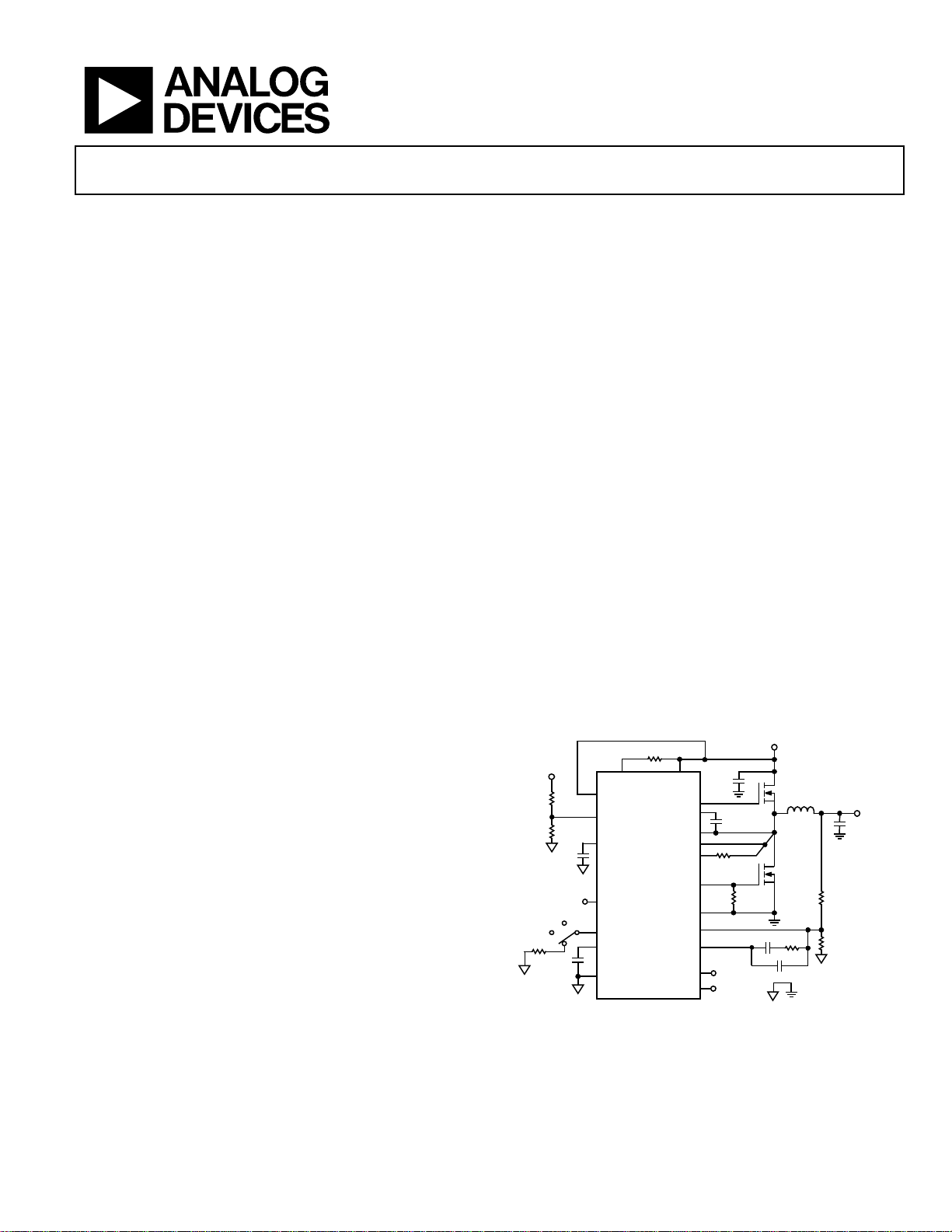
VIN
M2
M1
FB
SW
PGND
VIN
L
DH
BST
DL
R
CSG
R
RAMP
RAMP
PGOOD
SYNC
TRK
SS
ILIM
EN
COMP
CLKOUT
FREQ
VCCO
VOUT
ADP1853
HI
LO
CS
AGND
V
MA
10594-001
Data Sheet
FEATURES
Input voltage range: 2.75 V to 20 V
Output voltage range: 0.6 V to 90% V
Maximum output current of more than 25 A
Current mode architecture with current sense input
Configurable to voltage mode
±1% output voltage accuracy over temperature
Voltage tracking input
Programmable frequency: 200 kHz to 1.5 MHz
Synchronization input
Internal clock output
Power saving mode at light load
Precision enable input
Power good with internal pull-up resistor
Adjustable soft start
Programmable current sense gain
Integrated bootstrap diode
Starts into a precharged load
Externally adjustable slope compensation
Suitable for any output capacitor
Overvoltage and overcurrent-limit protection
Thermal overload protection
Input undervoltage lockout (UVLO)
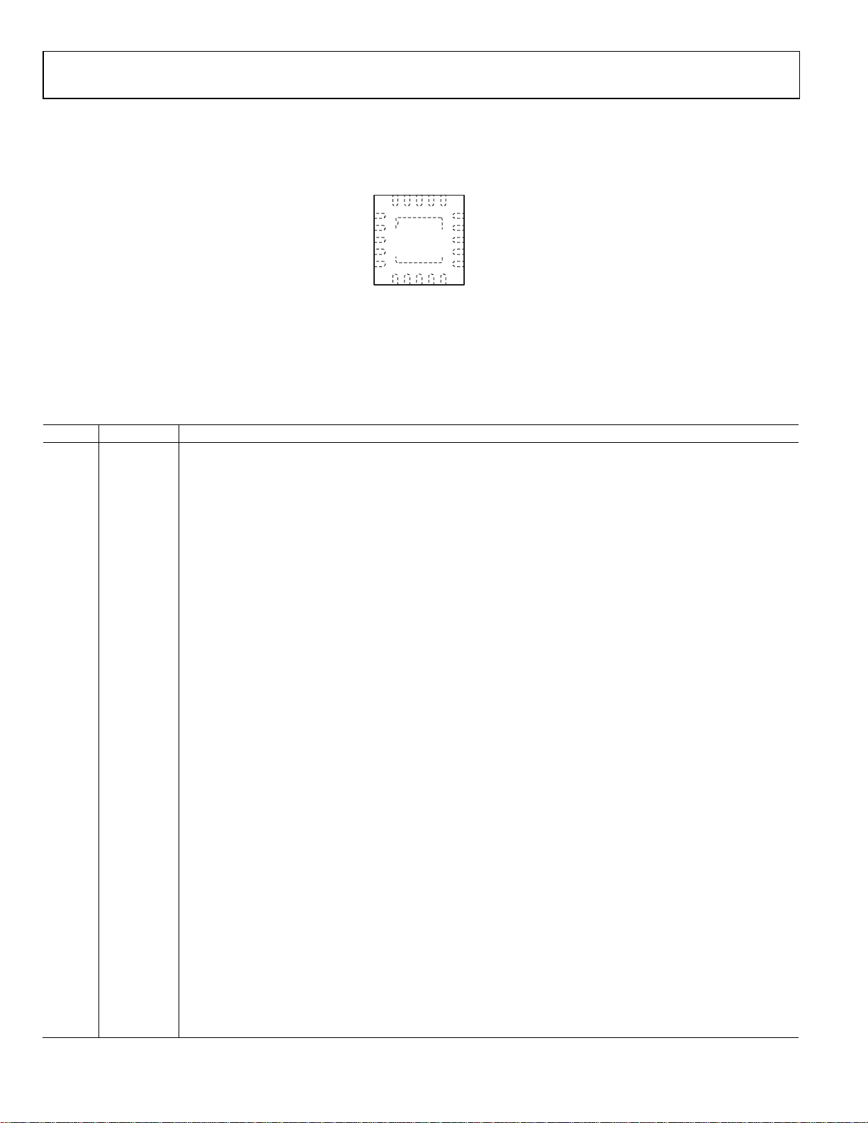
Available in 20-lead, 4 mm × 4 mm LFCSP
Supported by ADIsimPower™ design tool
APPLICATIONS
Intermediate bus and POL systems requiring sequencing and
tracking, including
Telecom base station and networking
Industrial and Instrumentation
Medical and healthcare
IN
current, improve EMI, and reduce the size of the input bulk
capacitance. The ADP1853 can also be configured as a slave
device for current sharing. Additionally, the ADP1853 includes
accurate tracking, precision enable, and power good functions
for sequencing. The ADP1853 provides a high speed, high peak
current gate driving capability to enable energy efficient power
conversion. The device can be configured to operate in power
saving mode by skipping pulses, reducing switching losses and
improving efficiency at light load and standby conditions.
The accurate current limit allows design within a narrower
range of tolerances and can reduce overall converter size and
cost. The ADP1853 can regulate down to 0.6 V output using a
high accuracy reference with ±1% tolerance over the
temperature range from −40°C to 125°C.
With a wide range input voltage, the ADP1853 is designed to
provide the designer with maximum flexibility for use in a
variety of system configurations; loop compensation, soft start,
frequency setting, power saving mode, current limit, and
current sense gain can all be programmed using external
components. In addition, the external RAMP resistor allows
choosing optimal slope and V
feedforward in both current
IN
and voltage mode for excellent line rejection. The linear
regulator and the boot strap diode for the high-side driver are
internal.
Protection features include undervoltage lock out, overvoltage,
overcurrent/short circuit, and overtemperature.
GENERAL DESCRIPTION
The ADP1853 is a wide range input, dc-to-dc, synchronous
buck controller capable of running from commonly used 3.3 V
to 12 V (up to 20 V) voltage inputs. The device nominally
operates in current mode with valley current sensing providing
the fastest step response for digital loads. It can also be
configured as a voltage mode controller with low noise and
crosstalk for sensitive loads.
The ADP1853 can be used as a master synchronization clock
for the power system and for convenient synchronization
between controllers. The CLKOUT signal can synchronize
other devices in the ADP185x family such that slave devices
are phase-shifted from the master to reduce the input ripple
responsibility is assumed by Analog Devices for its use, nor for any infringements of patents or other
rights of third parties that may result from its use. Specifications subject to change without n otice. No
license is granted by implication or otherwise under any patent or patent rights of Analog Devices.
One Technology Way, P.O. Box 9106, Norwood, MA 02062-9106, U.S.A.
Tel: 781.329.4700
Figure 1. Typical Operation Circuit
www.analog.com
Page 2

ADP1853 Data Sheet
TABLE OF CONTENTS
Features .............................................................................................. 1
Applications ....................................................................................... 1
General Description ......................................................................... 1
Revision History ............................................................................... 2
Specifications ..................................................................................... 3
Absolute Maximum Ratings ............................................................ 6
ESD Caution .................................................................................. 6
Simplified Block Diagram ............................................................... 7
Pin Configuration and Function Descriptions ............................. 8
Typical Performance Characteristics ........................................... 10
Theory of Operation ...................................................................... 12
Control Architecture .................................................................. 12
Oscillator Frequency .................................................................. 12
Synchronization .......................................................................... 13
PWM or Pulse Skip Mode of Operation ................................. 13
CLKOUT Signal .......................................................................... 13
Synchronous Rectifier and Dead Time ................................... 14
Input Undervoltage Lockout ..................................................... 14
Internal Linear Regulator .......................................................... 14
Overvolage Protection ............................................................... 14
Power Good ................................................................................. 14
Short-Circuit and Current-Limit Protection .......................... 15
Enable/Disable Control ............................................................. 15
Thermal Overload Protection .................................................. 16
Interleaved Dual-Phase Operation .......................................... 16
Applications Information .............................................................. 17
ADIsimPower Design Tool ....................................................... 17
Setting the Output Voltage ........................................................ 17
Soft Start ...................................................................................... 17
Setting the Current Limit .......................................................... 17
Accurate Current-Limit Sensing .............................................. 17
Input Capacitor Selection .......................................................... 17
VIN Pin Filter ............................................................................. 18
Boost Capacitor Selection ......................................................... 18
Inductor Selection ...................................................................... 18
Output Capacitor Selection....................................................... 18
MOSFET Selection ..................................................................... 19
Loop Compensation—Voltage Mode ...................................... 20
Loop Compensation—Current Mode ..................................... 21
Switching Noise and Overshoot Reduction ............................ 23
Voltage Tracking ......................................................................... 23
PCB Layout Guidlines ............................................................... 24
Typical Operating Circuits ............................................................ 25
Outline Dimensions ....................................................................... 27
Ordering Guide .......................................................................... 27
REVISION HISTORY
5/12—Revision 0: Initial Version
Rev. 0 | Page 2 of 28
Page 3

Data Sheet ADP1853
POWER SUPPLY
TRSH
HYST
Quiescent Current
IIN
EN = VIN = 12 V, VFB = V
in forced pulse width
4.2
5.7
mA
CCO
IN_SD
TRK
TRK
CSG
CSG
CSG
CSG
Line Regulation of PWM
VFB/VIN
±0.015
%/V
COMP
COMP
OSCILLATOR
OSC
FREQ
FREQ
FREQ
SYNC
FREQ
SYNCMIN
SYNC
CLKOUT fOSC
CLKOUT
CLKOUT
VCCO
VCCO Load Regulation
I
VCCO
= 0 mA to 100 mA
35 mV
VCCO
DROPOUT
VCCO
SPECIFICATIONS
All limits at temperature extremes are guaranteed via correlation using standard statistical quality control (SQC). VIN = 12 V. The
specifications are valid for T
Table 1.
Parameter Symbol Test Conditions/Comments Min Typ Max Unit
Input Voltage VIN 2.75 20 V
Undervoltage Lockout Threshold UVLO
VIN falling 2.35 2.45 2.50 V
Undervoltage Lockout Hysteresis UVLO
EN = VIN = 12 V, VFB = V
Shutdown Current I
ERROR AMPLIFIER
FB Input Bias Current IFB −100 +1 +100 nA
Open-Loop Gain1 80 dB
Gain-Bandwidth Product1 20 MHz
TRK Input Bias Current I
CURRENT SENSE AMPLIFIER GAIN ACS Gain resistor connected to DL,
Gain resistor connected to DL,
Default setting, R
Voltage mode operation, resistor DL to PGND,
OUTPUT CHARACTERICTISTICS
Feedback Accuracy Voltage VFB
= −40°C to +125°C, unless otherwise specified. Typical values are at TA = 25°C.
J
VIN rising 2.55 2.65 2.75 V
0.2 V
modulation (PWM) mode (no switching)
CCO
in PSM mode 2.5 mA
EN = GND, VIN = 5.5 V or 20 V 100 200 µA
0 V ≤ V
≤ 5 V −100 +1 +100 nA
2.6 3 3.4 V/V
R
= 47 kΩ ± 5%
5.2 6 6.8 V/V
R
= 22 kΩ ± 5%
= open 10.5 12 13.5 V/V
0 V/V
R
= 100 kΩ ± 5%
TJ = −40°C to +85°C
TJ = −40°C to +125°C
597 600 603 mV
594 600 606 mV
Load Regulation of PWM1 VFB/V
Frequency f
R
R
R
V
range = 0.9 V to 2.2 V ±0.3 %
= 332 kΩ to AGND 170 200 230 kHz
= 78.7 kΩ to AGND 720 800 880 kHz
= 40.2 kΩ to AGND 1275 1500 1725 kHz
FREQ to AGND 240 300 360 kHz
FREQ to VCCO 480 600 720 kHz
SYNC Input Frequency Range1 f
SYNC Input Pulse Width1 t
SYNC Pin Capacitance to GND C
CLKOUT Frequency Range1 f
CLKOUT Pulse Duty Cycle D
CLKOUT Rise and Fall Time C
R
range from 332 kΩ to 40.2 kΩ 170 1725 kHz
100 ns
5 pF
range from 170 kHz to 1725 kHz 170 1725 kHz
50 %
= 47 pF 10 ns
LINEAR REGULATOR
VCCO Output Voltage I
VCCO Line Regulation VIN = 5.5 V to 20 V, I
= 100 mA 4.7 5.0 5.3 V
= 20 mA 10 mV
VCCO Current Limit1 VCCO drops to 4 V from 5 V 350 mA
VCCO Short-Circuit Current1 VCCO < 0.5 V 370 400 mA
VIN to VCCO Dropout Voltage2 V
I
= 100 mA, VIN ≤ 5 V 0.33 V
Rev. 0 | Page 3 of 28
Page 4

ADP1853 Data Sheet
SYNC Logic Input Low
1.3
V
SYNC
BST
BST
DH or DL Driver RON, Sourcing
R
Sourcing 2 A with a 100 ns pulse
2
Ω
RON
OSC
OSC
OSC
OSC
OSC
COMP, THRES
COMP, HIGH
OVERVOLTAGE AND POWER GOOD
TRK
SOFT START
Parameter Symbol Test Conditions/Comments Min Typ Max Unit
LOGIC INPUTS
EN EN rising 0.57 0.63 0.68 V
EN Hysteresis 0.03 V
EN Input Leakage Current IEN VIN = 2.75 V to 20 V 1 200 nA
SYNC Logic Input High 1.9 V
SYNC Input Pull-Down Resistance R
GATE DRIVERS
DH Rise Time CDH = 3 n F, V
DH Fall Time CDH = 3 n F, V
DL Rise Time CDL = 3 nF 16 ns
DL Fall Time CDL = 3 nF 14 ns
DH to DL Dead Time External 3 nF is connected to DH and DL 25 ns
Current1
Sourcing 1 A with a 100 ns pulse, VIN = 3 V 2.3 Ω
DH or DL Driver RON, Tem p co TC
DH or DL Driver RON, Sinking
Current
1
Sinking 1 A with a 100 ns pulse, VIN = 3 V 2 Ω
DH Maximum Duty Cycle1 f
DH Maximum Duty Cycle1 f
Minimum DH On Time f
Minimum DH Off Time f
Minimum DL On Time f
COMP VOLTAGE RANGE
COMP Pulse Skip Threshold V
COMP Clamp High Voltage V
THERMAL SHUTDOWN
Thermal Shutdown Threshold T
Thermal Shutdown Hysteresis 20
1 MΩ
− VSW = 5 V 16 ns
− VSW = 5 V 14 ns
ON_SOURCE
VIN = 3 V or 12 V 0.3 %/oC
Sinking 2 A with a 100 ns pulse 1.5 Ω
R
ON_SINK
= 300 kHz 90 %
= 1500 kHz 50 %
= 200 kHz to 1500 kHz 85 ns
= 200 kHz to 1500 kHz 345 ns
= 200 kHz to 1500 kHz 295 ns
In pulse skip mode (PSM) 0.9 V
2.2 V
155
TMSD
°C
°C
THRESHOLDS
FB Overvoltage Threshold VOV VFB rising 0.630 0.65 0.670 V
FB Overvoltage Hysteresis 18 mV
FB Undervoltage Threshold VUV VFB falling 0.525 0.55 0.575 V
FB Undervoltage Hysteresis 15 mV
TRK INPUT VOLTAGE RANGE1 0 5 V
FB TO TRK OFFSET VOLTAGE TRK = 0.1 V to 0.57 V; offset = VFB − V
SS Output Current ISS During startup 4.6 6.5 8.4 µA
SS Pull-Down Resistor During a fault condition 3 kΩ
FB to SS offset VSS = 0.1 V to 0.6 V; offset = VFB − VSS −10 +10 mV
−10 0 +10 mV
Rev. 0 | Page 4 of 28
Page 5
Data Sheet ADP1853
PGOOD
Parameter Symbol Test Conditions/Comments Min Typ Max Unit
PGOOD
PGOOD Pull-Up Resistor R
PGOOD Delay 12 µs
Overvoltage or Undervoltage
Minimum Duration
ILIM Threshold Voltage1 Relative to PGND −5 0 +5 mV
ILIM Output Current ILIM = PGND 45 50 55 µA
Current Sense Blanking Period After DL goes high, current limit is not sensed
INTEGRATED RECTIFIER
(BOOST DIODE) RESISTANCE
ZERO CURRENT CROSS OFFSET
(SW TO PGND)
1
Guaranteed by design.
2
Connect VIN to VCCO when VIN < 5.5 V.
1
Internal pull-up resistor to VCCO 12.5 kΩ
This is the minimum duration required to trip
10 µs
the PGOOD signal
100 ns
during this period
At 20 mA forward current 16 Ω
In pulse skip mode only; f
= 300 kHz 0 2 4 mV
OSC
Rev. 0 | Page 5 of 28
Page 6
ADP1853 Data Sheet
BST to SW
−0.3 V to +6 V
BST to PGND to PGND 20 ns Transients
32 V
1, 2
ABSOLUTE MAXIMUM RATINGS
Table 2.
Parameter Rating
VIN, EN, RAMP 21 V
FB, COMP, SS, TRK, FREQ, SYNC, VCCO,
−0.3 V to +6 V
PGOOD, CLKOUT
ILIM, SW, CS to PGND −0.3 V to +21 V
BST, DH to PGND −0.3 V to +28 V
DL to PGND −0.3 V to VCCO + 0.3 V
SW, CS to PGND 20 ns Transients 25 V
DL, SW, CS, ILIM to PGND 20 ns
−8 V
Negative Transients
PGND to AGND −0.3 V to +0.3 V
PGND to AGND 20 ns Transients −8 V to +4 V
θJA (Natural Convection)
40°C/W
Operating Junction Temperature Range3 −40°C to +125°C
Storage Temperature Range −65°C to +150°C
Maximum Soldering Lead Temperature 260°C
1
Measured with exposed pad attached to PCB.
2
Junction-to-ambient thermal resistance (θJA) of the package was calculated
or simulated on multilayer PCB.
3
The junction temperature (TJ) of the device is dependent on the ambient
temperature (T
ambient thermal resistance of the package (θ
temperature is calculated from the ambient temperature and power
dissipation using the formula T
) the power dissipation of the device (PD) and the junction to
A
= TA + PD × θJA.
J
). Maximum junction
JA
Stresses above those listed under Absolute Maximum Ratings
may cause permanent damage to the device. This is a stress
rating only; functional operation of the device at these or any
other conditions above those indicated in the operational
section of this specification is not implied. Exposure to absolute
maximum rating conditions for extended periods may affect
device reliability.
Absolute maximum ratings apply individually only, not in
combination. Unless otherwise specified, all other voltages are
referenced to GND.
ESD CAUTION
Rev. 0 | Page 6 of 28
Page 7
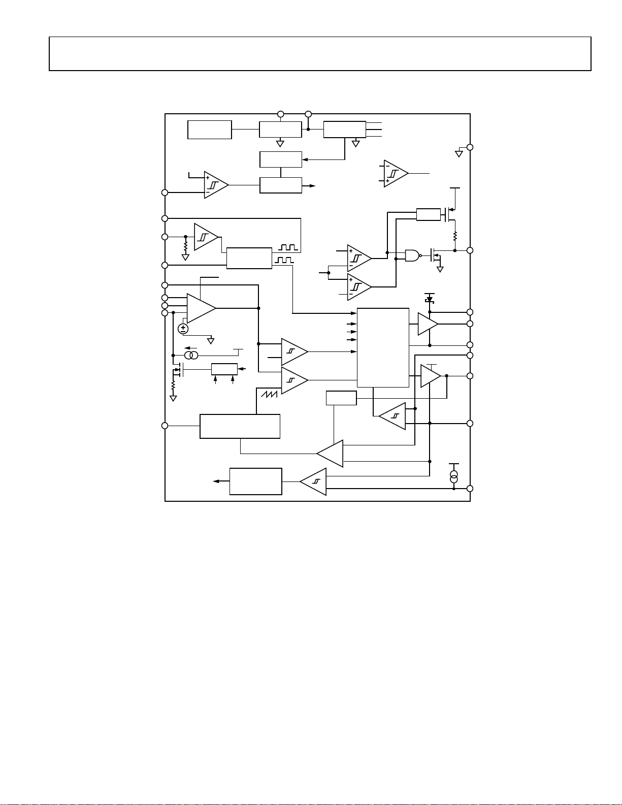
Data Sheet ADP1853
BST
PGND
+
–
+
–
+
–
+
–
FB
OV_TH
UV_TH
PGOOD
CURRENT SENSE
AMPLIFIER
DH
DL
ILIM
SW
V
REF
= 0.6V
+
+
–
ERROR
AMPLIFIER
FB
COMP
SS
PWM
COMPARATOR
SLOPE COMPENSATION
AND RAMP GENERAT OR
CURRENT-LIMIT
CONTROL
RAMP
50µA
OV
+
TRK
CS GAIN
DRIVER LOGIC
CONTROL AND
STATE
MACHINE
OVER_LIM
PULSE SKIP
OVER_LIM
LDO
LOGIC
EN
VIN
UVLO
OSCILLATOR
FREQ
SYNC
REF
VCCO
OV
UV
0.6V
THERMAL
SHUTDOWN
AGND
CS
FAULT
OV
LOGIC
OVER_LIM
OV
EN
EN_SW
LOGIC
UV
3kΩ
0.9V
DCM
*0 (ZERO) GAIN IS FOR VOLTAGE MODE WITH RAMP FROM 0.7V TO 2.2V.
ZERO
CROSS
DETECT
12.5kΩ
A
V
= 0,* 3, 6, 12
VCCO
CLK
EN_SW
1MΩ
–
+
CLKOUT
VCCO
VCCO
VCCO
VCCO
SLAVE
SL_TH
FB
SLAVE
0.6V
6.5µA
10594-002
SIMPLIFIED BLOCK DIAGRAM
Rev. 0 | Page 7 of 28
Figure 2.
Page 8
ADP1853 Data Sheet
15
BST
Boot Strapped Upper Rail of High-Side Internal Driver. Connect a 0.1 µF to a 0.22 µF multilayer ceramic capacitor
14
13
12
1
3
4
DH
15
BST
NOTES
1. CONNECT THE BOTTOM OF THE
EXPOSED PAD TO THE SYSTEM
AGND PLANE.
SW
CS
11
DL
EN
FB
2
SS
COMP
5
AGND
7
CLKOUT
6
SYNC
8
VIN
9
VCCO
10
PGND
19
FREQ
20
TRK
18
RAMP
17
PGOOD
16
ILIM
ADP1853
TOP VIEW
10594-003
PIN CONFIGURATION AND FUNCTION DESCRIPTIONS
Figure 3. Pin Configuration
Table 3. Pin Function Descriptions
Pin No. Mnemonic Description
1 EN Enable Input. Drive EN high to turn on the controller, and drive EN low to turn the controller off. Tie EN to VIN for
automatic startup. For a precision UVLO, put an appropriately sized resistor divider from V
midpoint to this pin.
2 SS Soft Start Input. Connect a capacitor from SS to AGND to set the soft start period. This node is internally pulled up
to VCCO through a 6.5 µA current source.
3 FB Output Voltage Feedback. Connect this pin to an output via a resistor divider. Tie FB to VCCO for slave mode
operation in interleaved dual-phase configuration.
4 COMP Compensation Node. Output of the error amplifier. Connect a resistor-capacitor network from COMP to FB to
compensate the regulation control loop. In interleaved dual-phase configuration, tie this pin to the COMP pin of
the second channel.
5 AGND Analog Ground. Connect to the system AGND plane.
6 SYNC Frequency Synchronization Input. This pin accepts an external clock signal with a frequency close to 1× the
internal oscillator frequency, f
, set by the FREQ pin. The controller operates in forced PWM when a periodic clock
OSC
signal is detected at SYNC or when SYNC is high. The resulting switching frequency is 1× the SYNC frequency.
When SYNC is low or left floating, the controller operates in pulse skip mode.
7 CLKOUT
Internal Clock Output. The CLKOUT is 1× the internal oscillator or input SYNC signal frequency, 180° phase-shifted.
This pin can be used to synchronize another
ADP1853 or other controllers.
8 VIN Connect to Main Power Supply. Bypass with a 1 µF or larger ceramic capacitor connected as close to this pin as
possible and AGND.
9 VCCO Output of the Internal Low Dropout Regulator (LDO). The internal circuitry and gate drivers are powered from
VCCO. Bypass VCCO to AGND with a 1 μF or larger ceramic capacitor. The VCCO output remains active even when
EN is low. For operations at V
below 5 V, VIN may be jumped to VCCO. Do not use the LDO to power other auxiliary
IN
system loads.
10 PGND Power Ground. Ground for internal driver. Differential current.
11 DL Low-Side Synchronous Rectifier Gate Driver Output. To program the gain of the current sense amplifier in a current
mode or to set voltage mode control, connect a resistor between DL and PGND. This pin is capable of driving
MOSFETs with a total input capacitance up to 20 nF.
12 CS Current Sense Amplifier Input. Differential current is sensed between CS and PGND. Connect this pin to the
current sense resistor or to the SW pin to sense the current. Tie this pin to PGND for voltage mode operation.
13 SW Power Switch Node. Connect this pin to the source of the high-side N-channel MOSFET and the drain of the low-
14 DH High-Side Switch Gate Driver Output. This pin is capable of driving MOSFETs with a total input capacitance up to
16 ILIM Current-Limit Sense Comparator Inverting Input. Connect a resistor between ILIM and SW to set the current-
side N-channel MOSFET.
20 nF.
(MLCC) between BST and SW. There is an internal boost diode rectifier connected between VCCO and BST.
limit offset. For accurate current-limit sensing, connect ILIM to a current sense resistor at the source of the
low-side MOSFET.
Rev. 0 | Page 8 of 28
to AGND, and tie the
IN
Page 9

Data Sheet ADP1853
Pin No. Mnemonic Description
17 PGOOD Power Good. The open-drain power good indicator logic output with an internal 12.5 kΩ resistor is connected
between PGOOD and VCCO. PGOOD is pulled to ground when the output is outside the regulation window. An
external pull-up resistor is not required. If the controller is configured as a slave in the interleaved dual-phase
application by tying the FB pin high to VCCO, the pulse skip mode is enabled by driving the PGOOD pin low
externally in cases when the master is in pulse skip mode at light loads. Otherwise, if the master is configured to
forced PWM operation, PGOOD of the slave controller must be connected to the PGOOD of the master.
18 RAMP Programmable Current Setting for Slope Compensation. Connect a resistor from RAMP to VIN. The voltage at RAMP
is 0.2 V during operation. This pin is high impedance when the channel is disabled.
19 FREQ Internal Oscillator Frequency, f
resistor between FREQ and AGND. Connect FREQ to AGND for a preprogrammed 300 kHz or tie FREQ to VCCO for
600 kHz operating frequency.
20 TRK Tracking Input. Connect TRK to VCCO if tracking is not used.
EPAD Exposed Pad. Connect the bottom of the exposed pad to the system AGND plane.
. Sets the desired operating frequency between 200 kHz and 1.5 MHz with one
OSC
Rev. 0 | Page 9 of 28
Page 10

ADP1853 Data Sheet
PULSE SKIP
FORCED PW M
100
90
80
70
60
50
40
30
20
10
0
EFFICIENCY (%)
0.1 1 10 100
LOAD (A)
10594-004
CH2 200mV M 100µs 5.0MS/ s
200ns/pt
A CH4 14.2A
2
4
CH4 10A Ω
B
W
B
W
LOAD
CURRENT
VOUT_AC
10594-006
CH2 100mV
M 100µs 250MS/s
4ns/pt
A CH1 12.6V
1
2
CH1 5V
B
W
B
W
VIN
VOUT_AC
10594-008
PULSE SKIP
FORCED PW M
100
90
80
70
60
50
40
30
20
10
0
EFFICIENCY (%)
0.1 1 10 100
LOAD (A)
10594-005
CH2 200mV M 100µs 5.0MS/s
200ns/pt
A CH4 14.2A
4
2
CH4 10A Ω
B
W
B
W
LOAD
CURRENT
VOUT_AC
10594-007
CH2 100mV
M 100µs 250MS/s
4ns/pt
A CH1 12.6V
1
2
CH1 5V
B
W
B
W
VIN
VOUT_AC
10594-009
TYPICAL PERFORMANCE CHARACTERISTICS
12 V
to 3.3 V
IN
, 300 kHz, see Figure 36 for Circuit
OUT
Figure 5. 10 A to 20 A Load Step,
12 V
to 3.3 V
IN
OUT
Figure 4. Efficiency Plot
, 300 kHz, Current Mode
15 V
to 5 V
IN
, 600 kHz, see Figure 35 for Circuit
OUT
Figure 8. 10 A to 20 A Load Step,
12 V
Figure 7. Efficiency Plot
to 3.3 V
IN
, 300 kHz, Voltage Mode
OUT
Figure 6. 9 V to 15 V Line Step,
3.3 V
, 15 A Load, Current Mode
OUT
Figure 9. 9 V to 15 V Line Step,
3.3 V
, 15 A Load, Voltage Mode
OUT
Rev. 0 | Page 10 of 28
Page 11

Data Sheet ADP1853
CH3 10V
M 1.0µs 1.25GS /s
400ps/pt
A CH1 3.6V
1
2
3
CH1 5V
B
W
B
W
CH2 5V
B
W
CLKOUT
DH
SYNC
10594-016
25
35
34
33
32
31
30
29
28
27
26
–40 –20 0 20 40 60 80 100 120 140
DEAD TIME ( ns)
TEMPERATURE (°C)
VIN = 12V
OUTPUT IS LOADED
HS FET = BS C080N03LS
LS FET = BS C030N03LS
DEAD TIME BETWEEN SW FALLING EDGE
AND DL RISING EDGE, I NCLUDING DIODE RECOVERY TIME
10594-011
50
100
150
200
250
300
350
2.5 5.0 7.5 10.0 12.5 15.0 17.5 20.0
TIME (ns)
DH MINIMUM OFF TIME
DH MINIMUM ON TIME
VIN (V)
10594-012
CH3 10V
M 2ms 250kS/s
4µs/pt
A CH1 560mV
1
2
3
CH1 2V
B
W
CH2 1V
B
W
B
W
EN
VOUT
SW
10594-017
25
45
43
41
39
37
35
33
31
29
27
0 2015105
DEAD TIME ( ns)
VIN (V)
T
A
= 25°C
OUTPUT IS LOADED
HS FET = BS C080N03LS
LS FET = BS C030N03LS
DEAD TIME BETWEEN SW FALLING EDGE
AND DL RISING EDGE, I NCLUDING DIODE RECOVERY TIME
10594-014
0
0.5
1.0
1.5
2.0
2.5
3.0
3.5
4.0
4.5
–40 –15 10 35 60 85 110 135
DRIVER RESI STANCE (Ω)
TEMPERATURE (°C)
VIN = 2.75V, SOURCING
VIN = 12V, SOURCING
VIN = 2.75V, SINKING
VIN = 12V, SINKING
10594-015
Figure 10. Synchronization and CLKOUT, f
Figure 11. Dead Time vs. Temperature
= 300 kHz
SYNC
Figure 13. Soft Start with Precharged Output, 3.3 V
Forced PWM
OUT
Figure 14. Dead Time vs. V
IN
Figure 12. Typical DH Minimum On Time and Off Time
Figure 15. Driver Resistance vs. Temperature
Rev. 0 | Page 11 of 28
Page 12

ADP1853 Data Sheet
065.1
)kHz(568,96)kΩ(
−
×=
OSCFREQ
fR
FREQ
OSC
FF
OSC
Q
Q
R
S
A
CS
V
CS
V
IN
V
IN
A
R
I
RAMP
R
RAMP
C
R
FROM
ERROR AMP
TO
DRIVERS
CS
PGND
10594-022
410
R
FREQ
(kΩ)
360
310
260
210
160
110
60
10
100 400 700 1000 1300 1600 1900
f
OSC
(kHz)
R
FREQ
(kΩ) = 96,568
f
OSC
(kHz)
–1.065
10594-023
THEORY OF OPERATION
The ADP1853 is a fixed frequency, step-down, synchronous
switching controller with integrated drivers and bootstrapping
for external N-channel power MOSFETs. The current mode
control loop can also be configured into the voltage mode. The
controller can be set to operate in pulse skip mode for power
saving at a light load or in forced PWM. The ADP1853 includes
programmable soft start, output overvoltage protection, programmable current limit, power good, and tracking functions.
The controller can operate at a switching frequency between
200 kHz and 1.5 MHz that is programmed with a resistor or
synchronized to an external clock. It also has the internal clock
out signal that can be used to synchronize other devices.
CONTROL ARCHITECTURE
The ADP1853 is based on a fixed frequency, emulated peak
current mode, PWM control architecture. The inductor current
is sensed by the voltage drop measured across the external lowside MOSFET, R
between the low-side MOSFET source and the power ground.
The current is sensed during the off period of the switching
cycle and is conditioned with the internal current sense
amplifier. The gain of the current sense amplifier is programmable to 3 V/V, 6 V/V, or 12 V/V during the controller
power-up initialization before the device starts switching. A
47 kΩ resistor between DL and PGND programs the gain of
3 V/V; a 22 kΩ resistor sets a gain of 6 V/V. Without a resistor,
the gain is programmed to 12 V/V. The output signal of the
current sense amplifier is held, added to the emulated current
ramp in the next switching cycle during the DH on time, and
fed into the PWM comparator, as shown in Figure 16. This
signal is compared with the COMP signal from the error
amplifier and resets the flip-flop, which generates the PWM
pulse. If voltage mode control is selected by placing a 100 kΩ
resistor between DL and PGND, the emulated ramp is fed to the
PWM comparator without adding the current sense signal.
, or across the sense resistor placed in series
DSON
As shown in Figure 16, the emulated current ramp is generated
inside the IC, but offers programmability through the RAMP
pin. Selecting an appropriate value resistor between V
to the
IN
RAMP pin programs a desired slope compensation value, and at
the same time, provides a V
feed forward feature. Control
IN
logic enforces antishoot-through operation to limit cross
conduction of the internal drivers and external MOSFETs.
OSCILLATOR FREQUENCY
The internal oscillator frequency, which ranges from 200 kHz
to 1.5 MHz, is set by an external resistor, R
pin. Some popular f
values are shown in Table 4, and a
OSC
graphical relationship is shown in Figure 17. For instance, a 78.7
kΩ resistor sets the oscillator frequency to 800 kHz.
Furthermore, connecting FREQ to AGND or FREQ to VCCO
sets the oscillator frequency to 300 kHz or 600 kHz,
respectively. For other frequencies that are not listed in Table 4,
the values of R
and f
can be obtained from Figure 17, or use the following
OSC
FREQ
empirical formula to calculate these values:
Table 4. Setting the Oscillator Frequency
R
f
332 kΩ 200 kHz
78.7 kΩ 800 kHz
60.4 kΩ 1000 kHz
51 kΩ 1200 kHz
40.2 kΩ 1500 kHz
FREQ to AGND 300 kHz
FREQ to VCCO 600 kHz
, at the FREQ
FREQ
(Typical)
Figure 16. Simplified Control Architecture
Rev. 0 | Page 12 of 28
Figure 17. R
FREQ
vs. f
OSC
Page 13

Data Sheet ADP1853
CH2 200mVCH1 10V M200µs A CH1 7.8V
1
3
4
2
CH3 20mV CH4 2A Ω
SW
COMP (CH2)
VOUT RIPPLE
INDUCTOR
CURRENT
10594-024
CH2 5VCH1 10V M1µs A CH1 13.4V
1
3
4
2
CH3 20mV CH4 2A Ω
DH
DL
OUTPUT
RIPPLE
INDUCTOR CURRENT
10594-025
SYNCHRONIZATION
The switching frequency of the ADP1853 can be synchronized
to an external clock signal by connecting it to the SYNC pin.
The internal oscillator frequency, programmed by the resistor at
the FREQ pin must be set close to the external clock frequency;
therefore, the external clock frequency may vary between 0.85×
and 1.3× of the internal clock set. The resulting switching
frequency is 1× of the external SYNC frequency. When
synchronized, the ADP1853 operates in PWM.
When an external clock is detected at the first SYNC edge, the
internal oscillator is reset, and the clock control shifts to SYNC.
The SYNC edges then trigger subsequent clocking of the PWM
outputs. The DH rising edge appears approximately 100 ns after
the corresponding SYNC edge, and the frequency is locked to
the external signal. If the external SYNC signal disappears
during operation, the ADP1853 reverts to its internal oscillator.
When the SYNC function is used, it is recommended to connect a
pull-up resistor from SYNC to VCCO so that when the SYNC
signal is lost, the ADP1853 continues to operate in PWM.
PWM OR PULSE SKIP MODE OF OPERATION
The SYNC pin is a multifunctional pin. PWM mode is enabled
when SYNC is connected to VCCO or a high logic. With SYNC
connected to ground or left floating, pulse skip mode is
enabled. Switching SYNC from low to high or high to low on
the fly causes the controller to transition from forced PWM
to pulse skip mode or from pulse skip mode to forced PWM,
respectively, in two clock cycles.
Figure 18. Example of Pulse Skip Mode Under a Light Load
When the output load is greater than the pulse skip threshold
current, that is, when V
reaches the threshold of 0.9 V, the
COMP
ADP1853 exits the pulse skip mode of operation and enters
the fixed frequency discontinuous conduction mode (DCM),
as shown in Figure 19. When the load increases further, the
ADP1853 enters continuous conduction mode (CCM).
Table 5. Mode of Operation
SYNC Pin Mode of Operation
Low Pulse skip mode
High Forced PWM
No Connect Pulse skip mode
Clock Signal Forced PWM
Figure 19. Example of Discontinuous Conduction Mode (DCM) Waveform
The ADP1853 has pulse skip sensing circuitry that allows the
controller to skip PWM pulses, reducing the switching
frequency at light loads and, therefore, maintaining better
efficiency during a light load operation. The resulting output
ripple is larger than that of the fixed frequency forced PWM.
Figure 18 shows the ADP1853 operating in PSM under a light
load. Pulse skip frequency under a light load is dependent on
the inductor, output capacitance, output load, and input and
output voltages.
In forced PWM, the ADP1853 always operates in CCM at any
load; therefore, the inductor current is always continuous.
CLKOUT SIGNAL
The ADP1853 has a clock output, CLKOUT, which can be
used for synchronizing other ADP1853 controllers, thus
eliminating the need for an external clock source. The
CLKOUT frequency is 1× the internal oscillator frequency,
f
, and is 180° out of phase.
OSC
Rev. 0 | Page 13 of 28
Page 14

ADP1853 Data Sheet
ADP1853
VIN
V
IN
= 2.75V TO 5.5V
VCCO
10594-026
CH1 20V CH2 5V
CH3 1V CH4 10V
M100µs A CH1 10V
1
2
4
3
DH
PGOOD
VOUT = 1.8V SHORTE
D TO 2V SOURCE
VIN
10594-027
SYNCHRONOUS RECTIFIER AND DEAD TIME
In the ADP1853, the antishoot-through circuit monitors the
DH to SW and DL to PGND voltages and adjusts the low-side
and high-side drivers to ensure break-before-make switching
that prevents cross-conduction or shoot-through between
the high-side and low-side MOSFETs. This break-before-make
switching is known as dead time, which is not fixed and
depends on how fast the MOSFETs are turned on and off. In
a typical application circuit that uses medium sized MOSFETs
with an input capacitance of approximately 3 nF, the typical
dead time is approximately 25 ns. When small and fast
MOSF E Ts with fast diode recovery times are used, the dead
time can be as low as 13 ns.
INPUT UNDERVOLTAGE LOCKOUT
When the bias input voltage at the VIN pin is less than the
undervoltage lockout (UVLO) threshold of 2.6 V typical, the
switch drivers stay inactive. If EN is high, the controller starts
switching and the VIN pin voltage exceeds the UVLO
threshold.
INTERNAL LINEAR REGULATOR
The internal linear regulator is a low dropout (LDO) VCCO.
VCCO powers up the internal control circuitry and provides
power for the gate drivers. It is guaranteed to have more than
200 mA of output current capability, which is sufficient to
handle the gate driver requirements of typical logic threshold
MOSFETs driven at up to 1.5 MHz. VCCO is always active
and cannot be shut down by the EN signal; however, the overtemperature protection event disables the LDO together with
the controller. Bypass VCCO to AGND with a 1 µF or greater
capacitor.
Because the LDO supplies the gate driver current, the output of
VCCO is subject to sharp transient currents as the drivers
switch and the boost capacitors recharge during each switching
cycle. The LDO has been optimized to handle these transients
without overload faults. Due to the gate drive loading, using the
VCCO output for other external auxiliary system loads is not
recommended.
The LDO includes a current limit that is well above the
expected maximum gate driver load. This current limit also
includes a short-circuit foldback to further limit the VCCO
current in the event of a short-circuit fault.
For an input voltage of less than 5.5 V, it is recommended to
bypass the LDO by connecting VIN to VCCO, as shown in
Figure 20, thus eliminating the dropout voltage. However, if
the input range is 4 V to 7 V, the LDO cannot be bypassed by
shorting VIN to VCCO because the 7 V input has exceeded the
maximum voltage rating of the VCCO pin. In this case, use the
LDO to drive the internal drivers, but keep in mind that there is
a dropout when V
IN
is less t h an 5 V.
Figure 20. Configuration for V
< 5.5 V
IN
OVERVOLAGE PROTECTION
The ADP1853 has a built-in circuit for detecting output overvoltage at the FB node. When the FB voltage, V
, rises above
FB
the overvoltage threshold, the high-side N-channel MOSFET
(NMOSFET) is turned off, and the low-side NMOSFET is
turned on until the V
drops below the undervoltage threshold.
FB
This action is known as the crowbar overvoltage protection.
If the overvoltage condition is not removed, the controller
maintains the feedback voltage between the overvoltage and
undervoltage thresholds, and the output is regulated to within
typically +8% and −8% of the regulation voltage. During an
overvoltage event, the SS node discharges toward zero through
an internal 3 kΩ pull-down resistor. When the voltage at FB
drops below the undervoltage threshold, the soft start sequence
restarts. Figure 21 shows the overvoltage protection scheme in
action in PSM.
Figure 21. Overvoltage Protection in PSM
POWER GOOD
The PGOOD pin is an open-drain NMOSFET with an internal
12.5 kΩ pull-up resistor connected between PGOOD and
VCCO. PGOOD is internally pulled up to VCCO during
normal operation and is active low when tripped. When the
feedback voltage, V
or drops below the undervoltage threshold, the PGOOD output
is pulled to ground after a delay of 12 µs. The overvoltage or
undervoltage condition must exist for more than 10 µs for
PGOOD to become active. The PGOOD output also becomes
active if a thermal overload condition is detected.
Rev. 0 | Page 14 of 28
, rises above the overvoltage threshold
FB
Page 15

Data Sheet ADP1853
CH1 10V M2ms A CH1 11.2V
1
3
4
CH3 500mV CH4 10A Ω
SW
SS
INDUCTOR
CURRENT
10594-028
ADP1853
FBEN
R
TOP
R
BOT
V
OUT
R1
R2
MASTER
SUPPLY
VOLTAGE
10594-029
SHORT-CIRCUIT AND CURRENT-LIMIT PROTECTION
When the output is shorted or the output current exceeds the
current limit set by the current-limit setting resistor (between
ILIM and CS) for eight consecutive cycles, the ADP1853 shuts
off both the high-side and low-side drivers and restarts the soft
start sequence every 10 ms, which is known as hiccup mode.
The SS node discharges to zero through an internal 3 kΩ
resistor during an overcurrent or short-circuit event. Figure 22
shows that the ADP1853 on a high current application circuit
maintains current-limit hiccup mode when the output is
shorted.
ENABLE/DISABLE CONTROL
The EN pin is used to enable or disable the controller ADP1853;
the precision enable typical threshold is 0.63 V. When the
voltage at EN rises above the threshold voltage, the controller is
enabled and starts normal operation after initialization of the
internal oscillator, references, settings, and the soft start period.
When the voltage at EN drops to typically 30 mV (hysteresis)
below the threshold voltage, the driver and the internal
controller circuits in the ADP1853 are turned off. The initial
settings are still valid; therefore re-enabling the controller does
not change the settings until the power at the VIN pin is cycled.
In addition, the EN signal does not shut down the LDO at
VCCO, which is always active when V
threshold.
For the purpose of start-up power sequencing, the startup of the
ADP1853 can be programmed by connecting an appropriate
resistor divider from the master power supply to the EN pin, as
shown in Figure 23. For instance, if the desired start-up voltage
from the master power supply is 10 V, R1 and R2 can be set to
156 kΩ and 10 kΩ, respectively.
is above the UVLO
IN
Figure 22. Current-Limit Hiccup Mode, 20 A Current Limit
Figure 23. Optional Power-Up Sequencing Circuit
Rev. 0 | Page 15 of 28
Page 16

ADP1853 Data Sheet
VIN
M2
M1
FB
SW
PGND
V
IN
L1
DH
BST
DL
R
CSG
R
RAMP
RAMP
PGOOD
SYNC
TRK
SS
ILIM
EN
COMP
CLKOUT
FREQ
VCCO
V
OUT
ADP1853
CS
AGND
MASTER
VIN
M4
M3
FB
SW
PGND
V
IN
L2
DH
BST
DL
R
CSG
R
RAMP
RAMP
PGOOD
SYNC
TRK
SS
ILIM
EN
COMP
CLKOUT
FREQ
VCCO
ADP1853
CS
AGND
SLAVE
10594-030
THERMAL OVERLOAD PROTECTION
The ADP1853 has an internal temperature sensor that senses
the junction temperature of the chip. When the junction
temperature of the ADP1853 reaches approximately 155°C, the
ADP1853 goes into thermal shutdown, the converter is turned
off, and SS discharges toward zero through an internal 3 kΩ
resistor. At the same time, VCCO discharges to zero. When
the junction temperature drops below 135°C, the ADP1853
resumes normal operation after the soft start sequence.
INTERLEAVED DUAL-PHASE OPERATION
Two ADP1853 controllers can be configured to design a
dual-phase, interleaved, step-down, switching dc-to-dc
regulators. In dual-phase operation, the two outputs of the
switching regulators are tied together and can source more
than 50 A of output current depending on the selection of
the power components. See Figure 24 for a configuration of a
typical dual-phase application circuit. Note that only one error
amplifier, in the master ADP1853, works; the error amplifier in
the slave ADP1853 output is turned to tristate by tying FB to
VCCO. The CLKOUT signal from the master is connected to
the SYNC input of the slave controller; the SS signals of the
master and slave are tied together; COMP of the slave must be
tied to COMP of the master; and PGOOD of the slave must be
tied to PGOOD of the master.
Figure 24. Dual-Phase Application
Rev. 0 | Page 16 of 28
Page 17

Data Sheet ADP1853
−
=
FB
FB
OUT
BOTTOP
V
VV
RR
SSSS
Ct
μA5.
6
V6.0
=
μA50
06.1
CS
LPK
ILIM
RIR××
=
SWESRO
PP
O
MININ
fDRIV
DDI
C
)(
)1(
,
×−
−×
=
V
APPLICATIONS INFORMATION
ADIsimPower DESIGN TOOL
The ADP1853 is supported by the ADIsimPower design tool
set. ADIsimPower is a collection of tools that produce complete
power designs optimized to a specific design goal. The tools
allow the user to generate a full schematic, bill of materials, and
calculate performance in minutes. ADIsimPower can optimize
designs for cost, area, efficiency, and parts count while taking
into consideration the operating conditions and limitations of
the IC and all real external components. The ADIsimPower tool
can be found at www.analog.com/ADIsimPower and the user
can request an unpopulated board through the tool.
SETTING THE OUTPUT VOLTAGE
The output voltage is set using a resistive voltage divider from
the output to FB. For R
R
to set the output voltage by using the following equation:
TOP
, use a 1 kΩ to 20 kΩ resistor. Choose
BOT
where:
R
is the high-side voltage divider resistance.
TOP
R
is the low-side voltage divider resistance.
BOT
V
is the regulated output voltage.
OUT
V
is the feedback regulation threshold, 0.6 V.
FB
SOFT START
The soft start period is set by an external capacitor between
SS and AGND. The soft start function limits the input inrush
current and prevents output overshoot. When EN is enabled,
a current source of 6.5 µA starts charging the capacitor, and
the regulation voltage is reached when the voltage at SS reaches
0.6 V. The soft start time is approximated by
The SS pin reaches a final voltage equal to VCCO.
When a controller is disabled, for instance, if EN is pulled low
or experiences an overcurrent limit condition, the soft start
capacitor is discharged through an internal 3 kΩ pull-down
resistor.
SETTING THE CURRENT LIMIT
The current-limit comparator measures the voltage across the
low-side MOSFET to determine the load current.
The current limit is set by an external current-limit resistor,
R
, between ILIM and CS. The current sense pin, ILIM,
ILIM
sources nominally 50 μA to this external resistor. This creates
an offset voltage of R
across the current sense element R
side MOSFET, R
multiplied by 50 μA. When the drop
ILIM
(a sense resistor or low-
CS
) is equal to or greater than this offset
DSON
voltage, the ADP1853 flags a current-limit event.
where:
I
is the peak inductor current.
LPK
ACCURATE CURRENT-LIMIT SENSING
R
of the MOSFET can vary by more than 50% over the
DSON
temperature range. Accurate current-limit sensing is achieved
by adding a current sense resistor from the source of the lowside MOSFET to PGND. Make sure that the power rating of the
current sense resistor is adequate for the application. Figure 25
illustrates the implementation of accurate current-limit sensing.
IN
ADP1853
DH
CS
R
ILIM
ILIM
DL
R
SENSE
10594-031
Figure 25. Accurate Current-Limit Sensing
INPUT CAPACITOR SELECTION
Use two parallel capacitors placed close to the drain of the highside switch MOSFET (one bulk capacitor of sufficiently high
current rating and a 10 μF ceramic decoupling capacitor).
Select an input bulk capacitor based on its ripple current
rating. The minimum input capacitance required for a
particular load is
where:
IO is the output current.
D is the duty cycle.
V
is the desired input ripple voltage.
PP
R
is the equivalent series resistance of the capacitors.
ESR
Rev. 0 | Page 17 of 28
Page 18

ADP1853 Data Sheet
IN
OUT
L
SW
OUT
IN
V
V
If
VV
L ×
∆×
−
=
))4((
1
8
2
222
ESLSWESR
L
OUT
SW
L
OUT
LfRIV
f
I
C
×−×∆−∆
×
∆
≅
ESR
L
OUT
RIV ×∆≅∆
SW
OUT
L
OUT
fV
I
C
×∆
∆
≅
8
2
2
2
)(
OUTOVERSHOOTOUT
STEP
OUT
VVV
LI
C
−∆+
∆
≅
VIN
V
IN
AGND
2Ω TO 10Ω
1µF
ADP1853
10594-032
VIN PIN FILTER
It is recommended to have a low-pass filter at the VIN pin.
Connecting a resistor, between 2 Ω and 10 Ω, in series with
VIN and a 1 µF ceramic capacitor between VIN and AGND
creates a low-pass filter that effectively filters out any unwanted
glitches caused by the switching regulator. Keep in mind that
the input current could be larger than 100 mA when driving
large MOSFETs. A 100 mA across a 10 Ω resistor creates a 1 V
drop, which is the same voltage drop in VCCO. In this case, a
lower resistor value is desirable.
Figure 26. Input Filter Configuration
BOOST CAPACITOR SELECTION
Connect a boost capacitor between the SW and BST pins to
provide the current for the high-side driver during switching.
Choose a ceramic capacitor with a value between 0.1 µF and
0.22 µF.
INDUCTOR SELECTION
For most applications, choose an inductor value such that
the inductor ripple current is between 20% and 40% of the
maximum dc output load current.
Choose the inductor value by the following equation:
where:
L is the inductor value.
f
is the switching frequency.
SW
V
is the output voltage.
OUT
V
is the input voltage.
IN
∆I
is the peak-to-peak inductor ripple current.
L
Check the inductor data sheet to make sure that the saturation
current of the inductor is well above the peak inductor current
of a particular design.
OUTPUT CAPACITOR SELECTION
For maximum allowed switching ripple at the output, choose an
output capacitor that is larger than
where:
∆V
is the target maximum output ripple voltage.
OUT
∆I
is the inductor ripple current.
L
R
is the equivalent series resistance of the output capacitor
ESR
(or the parallel combination of ESR of all output capacitors).
L
is the equivalent series inductance of the output capacitor
ESL
(or the parallel combination of ESL of all capacitors).
The impedance of the output capacitor at the switching
frequency multiplied by the ripple current gives the output
voltage ripple. The impedance is made up of the capacitive
impedance plus the nonideal parasitic characteristics, the
equivalent series resistance (ESR), and the equivalent series
inductance (ESL).
Usually the capacitor impedance is dominated by ESR. The
maximum ESR rating of the capacitor, such as in electrolytic
or polymer capacitors, is provided in the manufacturer’s data
sheet; therefore, the output ripple reduces to
Electrolytic capacitors also have significant ESL, on the order
of 5 nH to 20 nH, depending on type, size, and geometry. PCB
traces contribute some ESR and ESL, as well. However, using
the maximum ESR rating from the capacitor data sheet usually
provides some margin such that measuring the ESL may not be
required.
In the case of output capacitors where the impedance of the
ESR and ESL are small at the switching frequency, for instance,
where the output capacitor is a bank of parallel MLCC capacitors, the capacitive impedance dominates, so the output
capacitance must be larger than
Make sure that the ripple current rating of the output capacitors
is greater than the maximum inductor ripple current.
To meet the requirement of the output voltage overshoot during
load release, the output capacitance should be larger than
where:
∆V
OVERS HOOT
Select the largest output capacitance given by either of the
previous two equations.
is the maximum allowed overshoot.
Rev. 0 | Page 18 of 28
Page 19

Data Sheet ADP1853
DSON
RMSLOAD
C
RIP ×=
2
)(
)(
SWG
PV
G
fQVP ××≅
2
)(
SW
FR
LOAD
IN
T
fttIV
P
×+××
≅
RISEDRIVER
GSW
R
I
Q
t
_
≅
FALLDRIVER
GSW
F
I
Q
t
_
≅
2
GS
GDGSW
Q
QQ +≅
GATE
SOURCEON
SP
DD
RISEDRIVER
RR
VV
I
+
−
≅
_
_
GATE
SINKON
SP
FALLDRIVER
RR
V
I
+
≅
_
_
T
CHS
PPP +≅
DSON
RMSLOAD
CLS
RIP ×=
2
)(
)(
If Q
MOSFET SELECTION
The choice of MOSFET directly affects the dc-to-dc converter
performance. A MOSFET with low on resistance reduces I
losses, and low gate charge reduces transition losses. The
MOSFET should have low thermal resistance to ensure that the
power dissipated in the MOSFET does not result in excessive
MOSFET die temperature.
The high-side MOSFET carries the load current during on time
and usually carries most of the transition losses of the converter.
Typically, the lower the on resistance of the MOSFET, the
higher the gate charge and vice versa. Therefore, it is important
to choose a high-side MOSFET that balances the two losses.
The conduction loss of the high-side MOSFET is determined
by the equation
where:
R
is the MOSFET on resistance.
DSON
The gate charging loss is approximated by the equation
where:
V
is the gate driver supply voltage.
PV
Q
is the MOSFET total gate charge.
G
Note that the gate charging power loss is not dissipated in the
MOSFET but rather in the ADP1853 internal drivers. This
power loss should be taken into consideration when calculating
the overall power efficiency.
The high-side MOSFET transition loss is approximated by the
equation
where:
P
is the high-side MOSFET switching loss power.
T
t
is the rise time in charging the high-side MOSFET.
R
t
is the fall time in discharging the high-side MOSFET.
F
t
and tF can be estimated by
R
2
R
is not given in the data sheet, it can be approximated by
GSW
where:
Q
and QGS are the gate-to-drain and gate-to-source charges
GD
given in the MOSFET data sheet.
I
DRIVER_RISE
and I
DR IV ER_ FAL L
can be estimated by
where:
VDD is the input supply voltage to the driver and is between
2.75 V and 5 V, depending on the input voltage.
V
is the switching point where the MOSFET fully conducts;
SP
this voltage can be estimated by inspecting the gate charge
graph given in the MOSFET data sheet.
R
ON_SOURCE
is the on resistance of the ADP1853 internal driver,
given in Table 1, when charging the MOSFET.
R
is the on resistance of the ADP1853 internal driver,
ON_SINK
given in Table 1, when discharging the MOSFET.
R
is the on gate resistance of MOSFET given in the
GAT E
MOSFET data sheet. If an external gate resistor is added, add
this external resistance to R
GATE
.
The total power dissipation of the high-side MOSFET is the
sum of conduction and transition losses:
The synchronous rectifier, or low-side MOSFET, carries the
inductor current when the high-side MOSFET is off. The lowside MOSFET transition loss is small and can be neglected in
the calculation. For high input voltage and low output voltage,
the low-side MOSFET carries the current most of the time.
Therefore, to achieve high efficiency, it is critical to optimize
the low-side MOSFET for low on resistance. In cases where the
power loss exceeds the MOSFET rating or lower resistance is
required than is available in a single MOSFET, connect multiple
low-side MOSFETs in parallel. The equation for low-side
MOSFET conduction power loss is
where:
Q
is the gate charge of the MOSFET during switching and is
GSW
given in the MOSFET data sheet.
I
DRIVER_RISE
and I
DRIVER_FALL
are the driver current output from the
ADP1853 internal gate drivers.
Rev. 0 | Page 19 of 28
Page 20

ADP1853 Data Sheet
OSW
DF
BODYDIODE
IftVP ×××=
BODYDIODECLSLS
PPP +=
RAMPSW
IN
RAMP
Vf
V
R
××
−
=
pF100
V2.0
μA160
V2.0
μA10 ≤
−
≤
RAMP
IN
R
V
LCπ
f
LC
2
1
=
10
SW
CO
f
f =
SW
P2P1
fff
2
1
==
I
Z
SWCO
Z2Z1
CR
ff
ff
π
2
1
404
====
I
Z
LC
Z2Z1
CR
f
ff
π
2
1
2
===
2
LC
IN
CO
Z1
RAMP
TOP
Z
fV
ffVR
R =
Z1Z
I
fRCπ=2
1
G
(dB)
PHASE
–90°
–270°
f
Z
f
P
C
HF
C
I
R
Z
R
FF
R
TOP
R
BOT
V
OUT
INTERNAL
VREF
EA
FB
COMP
–1 SLOPE
–1 SLOPE
C
FF
+1 SLOPE
10594-033
There is also additional power loss during the time, known as
dead time, between the turn-off of the high-side switch and the
turn-on of the low-side switch, when the body diode of the lowside MOSFET conducts the output current. The power loss in
the body diode is given by
where:
V
is the forward voltage drop of the body diode, typically 0.7 V.
F
t
is the dead time in the ADP1853, typically 30 ns when
D
driving a medium size MOSFETs with input capacitance, C
,
iss
of approximately 3 nF. The dead time is not fixed. Its effective
value varies with gate drive resistance and C
P
BODYDIODE
increases in high load current designs and low voltage
; therefore,
iss
designs.
Then the power loss in the low-side MOSFET is
Note that MOSFET on resistance, R
, increases with
DSON
increasing temperature with a typical temperature coefficient of
o
0.4%/
C. The MOSFET junction temperature (TJ) rise over the
ambient temperature is
T
= TA + θJA × P
J
D
where:
θ
is the thermal resistance of the MOSFET package.
JA
T
is the ambient temperature.
A
P
is the total power dissipated in the MOSFET.
D
LOOP COMPENSATION—VOLTAGE MODE
Set the controller to voltage mode operation by placing a
100 kΩ resistor between DL and PGND. Chose the larger
possible ramp amplitude for the voltage mode below 1.5 V.
The ramp voltage is programmed by a resistor value between
V
and the RAMP pin:
IN
Type III Compensation
Figure 27. Type III Compensation
If the output capacitor ESR zero frequency is greater than ½ of
the crossover frequency, use the Type III compensator as shown
in Figure 27.
Calculate the output LC filter resonant frequency as follows:
(2)
Chose a crossover frequency that is 1/10 of the switching
frequency:
(3)
Set the poles and zeros as follows:
(4)
(5)
The voltage at the RAMP pin is fixed at 0.2 V, and the current
going into RAMP should be between 10 µA and 160 µA. Make
sure that the following condition is satisfied:
For instance, with an input voltage of 12 V, R
less than 73.8 kΩ.
Assuming that the LC filter design is complete, the feedback
control system can be compensated. In general, aluminum
electrolytic capacitors have high ESR; however, if several
aluminum electrolytic capacitors are connected in parallel and
produce a low effective ESR, then Type III compensation is
needed. In addition, ceramic capacitors have very low ESR (only
a few milliohms) making Type III compensation a better choice.
or
(6)
Use the lower zero frequency from Equation 5 or Equation 6.
Calculate the compensator resistor, RZ, as follows:
(1)
(7)
should not be
RAMP
Next, calculate C
:
I
(8)
Because of the finite output current drive of the error amplifier,
CI needs to be less than 10 nF. If it is larger than 10 nF, choose a
larger R
and recalculate RZ and CI until CI is less than 10 nF.
TOP
Rev. 0 | Page 20 of 28
Page 21

Data Sheet ADP1853
Z
SW
HF
RfCπ
=
1
SW
FF
FF
fCRπ
=
1
CSCS
RAMP
RA
L
R
×
××
=
6
107
RAMPSW
IN
RAMP
Rf
V
V
××
−
=
pF100
V2.0
μA160
V2.0
μA10 ≤
−
≤
RAMP
IN
R
V
ADP1853
DH
CS
ILIM
DL
R
ILIM
R
CSG
RAMP
R
RAMP
V
IN
10594-034
Because CHF << CI, calculate CHF as follows:
(9)
The voltage at the RAMP pin is fixed at 0.2 V, and the current
going into RAMP should be between 10 µA and 160 µA. Make
sure that the following condition is satisfied:
Next, calculate the feedforward capacitor, C
R
:
TOP
, assuming RFF <<
FF
(10)
Check that the calculated component values are reasonable.
For instance, capacitors smaller than about 10 pF should be
avoided. In addition, R
values less than 3 kΩ and CI values
Z
greater than 10 nF should be avoided. If necessary, recalculate
the compensation network with a different starting value for
R
. If RZ is too small or CI is too big, start with a larger value
TOP
for R
. This compensation technique should yield a good
TOP
working solution.
When precise compensation is needed, use the ADIsimPower
design tool.
LOOP COMPENSATION—CURRENT MODE
Compensate the ADP1853 error voltage loop in current mode
using Type II compensation.
Setting the Slope Compensation
In a current-mode control topology, slope compensation is
needed to prevent subharmonic oscillations in the inductor
current and to maintain a stable output. The external slope
compensation is implemented by summing the amplified sense
signal and a scaled voltage at the RAMP pin. To set the effective
slope compensation, connect a resistor (R
RAMP pin and the input voltage (V
). R
IN
) between the
RAMP
is calculated by
RAMP
For instance, with an input voltage of 12 V, R
exceed 1.1 MΩ. If the calculated R
10 µA, then select an R
value that produces between
RAMP
produces less than
RAMP
should not
RAMP
10 µA and 15 µA.
Figure 28 illustrates the connection of the slope compensation
resistor, R
, and the current sense gain resistor, R
RAMP
Figure 28. Slope Compensation and CS Gain Connection
CSG
.
where:
L is the inductor value measured in µH.
R
CS and PGND (for instance, R
maximum on resistance).
A
or 12 V/V.
Thus, the voltage ramp amplitude, V
where 100 pF is the effective capacitance of the internal ramp
capacitor, C
V
(mΩ) is resistance of the current sense element between
CS
is the low-side MOSFET
DSON_MAX
is the current sense amplifier gain and is 3 V/ V, 6 V/ V,
CS
, is:
RAMP
, with ±4% tolerance over the temperature and
RAMP
range.
IN
Rev. 0 | Page 21 of 28
Page 22

ADP1853 Data Sheet
V
Setting the Current Sense Gain
The voltage drop across the external low-side MOSFET is
sensed by a current sense amplifier by multiplying the peak
inductor current and the R
of the MOSFET. The result is
DSON
then amplified by a gain factor of 3 V/V, 6 V/V, or 12 V/V,
which is programmable by an external resistor, R
, connected
CSG
to the DL pin. This gain is sensed only during power-up and
not during normal operation. The amplified voltage is summed
with the slope compensation ramp voltage and fed into the
PWM controller for a stable regulation voltage.
The voltage range of the internal node, V
, is between 0.4 V
CS
and 2.2 V. Select the current sense gain such that the internal
minimum amplified voltage (V
maximum amplified voltage (V
or V
is not the same as V
CSMAX
to 2.2 V. Make sure that the maximum V
) is above 0.4 V and the
CSMIN
) is 2.1 V. Note that V
CSMAX
, which has a range of 0.85 V
COMP
(V
COMP
COMPMAX
CSMIN
) does
not exceed 2.2 V to account for temperature and part-to-part
, V
variations. See the following equations for V
V
:
COMPMAX
1
CSMIN
V
COMPMAX
V75.0
2
(V75.0
LOADMAXCSMAX
IN
pF100
R
L
)V2.0(
RAMP
ARIV
_
1
)
L
2
tV
ON
V
CSMAX
CSMIN
CSMINDSON
_
CSMAX
ARIIV
CSMAXDSON
, and
where:
is the minimum amplified voltage of the internal current
V
CSMIN
sense amplifier at zero output current.
is the peak-to-peak ripple current in the inductor.
I
L
R
is the low-side MOSFET minimum on resistance. The
DSON_MIN
zero current level voltage of the current sense amplifier is 0.75 V.
is the maximum amplified voltage of the internal current
V
CSMAX
sense amplifier at the maximum output current.
is the maximum output dc load current.
I
LOADMAX
V
t
ON
Replace R
element, R
is the maximum voltage at the COMP pin.
COMPMAX
is the high-side driver (DH) on time.
with the resistance value of the current sense
DSON
, if it is used.
CS
Type II Compensation
–
1
S
L
O
G
P
R
TOP
R
BOT
E
f
Z
R
Z
FB
INTERNAL
VREF
EA
–
1
S
L
O
P
E
f
P
C
HF
C
I
COMP
10594-035
(dB)
PHASE
–180°
–270°
OUT
Figure 29. Type II Compensation
In this case, use the circuit shown in Figure 29. Calculate the
compensation resistor, R
TOPZ
, with the following equation:
Z
2
S
fCRRR
(11)
CO
OUT
where:
f
is chosen to be 1/10 of fSW.
CO
= ACS × R
R
S
DSON_MIN.
ACS is the current sense gain of either 3 V/V, 6 V/V, or 12 V/V,
set by the gain resistor between DL and PGND.
R
If the current is sensed on a current sense resistor, R
is the low-side MOSFET minimum on resistance.
DSON_MIN
, then RCS
CS
becomes
RAR
CSCSS
Next, choose the compensation capacitor to set the compensation zero, f
, to the lesser of 1/5 of the crossover frequency or ½
Z1
of the LC resonant frequency
ff
f
Z1
SWCO
505
1
2
(12)
CR
I
Z
or
f
Z1
Solving for C
C
I
Solving for C
C
I
f
LC
2
1
2
in Equation 12 yields
I
25
fR
SW
Z
in Equation 13 yields
I
1
fR
LC
Z
(13)
CR
I
Z
(14)
(15)
Rev. 0 | Page 22 of 28
Page 23

Data Sheet ADP1853
SW
P1
ff
2
1
=
HF
Z
P1
CRfπ=2
1
Z
SW
HF
RfCπ
=
1
SWSNUB
IN
SNUB
fCVP ××=
2
+
+
=
TRKB
TRKT
BOT
TOP
MASTEROUT
SLAVEOUT
R
R
R
R
V
V
1
1
_
_
MASTER VOLTAGE
SLAVE VOLTAGE
TIME
VOLTAGE (V)
10594-037
ADP1853
FB
SS
TRK
R
BOT
10kΩ
R
TOP
20kΩ
1.1V
3.3V
V
OUT_MASTER
1.8V
V
OUT_SLAVE
R
TRKB
10kΩ
R
TRKT
20kΩ
C
SS
20nF
10594-038
Use the larger value of CI from Equation 14 or Equation 15.
Because of the finite output current drive of the error amplifier,
C
needs to be less than 10 nF. If it is larger than 10 nF, choose a
I
larger R
Next, choose the high frequency pole, f
and recalculate RZ and CI until CI is less than 10 nF.
TOP
, to be ½ of fSW.
P1
(16)
Because C
<< CI,
HF
(17)
Combine Equation 16 and Equation 17, and solve for C
,
HF
(18)
For maximally precise compensation solutions, use the
ADIsimPower design tool.
SWITCHING NOISE AND OVERSHOOT REDUCTION
To reduce voltage ringing and noise, it is recommended to add
an RC snubber between SW and PGND for high current
applications, as illustrated in Figure 30.
In most applications, R
typically 1.2 nF to 3 nF.
The size of the RC snubber components must be chosen
correctly to handle the power dissipation. The power dissipated
in R
SNUB
is
In most applications, a component size of 0805 for R
sufficient. The RC snubber does not reduce the voltage overshoot. A resistor, shown as R
helps to reduce overshoot and is generally between 2 Ω and
4 Ω. Adding a resistor in series, typically between 2 Ω and
4 Ω, with the gate driver also helps to reduce overshoot. If a
gate resistor is added, then R
is typically 2 Ω to 4 Ω, and C
SNUB
in Figure 30, at the BST pin
RISE
is not needed.
RISE
SNUB
SNUB
is
is
VOLTAGE TRACKING
The ADP1853 includes a tracking feature that tracks a master
voltage. In all tracking configurations, the output can be set as
low as 0.6 V for a given operating condition. The soft start time
setting of the master voltage should be longer than the soft start
of the slave voltage. This forces the rise time of the master
voltage to be imposed on the slave voltage. If the soft start
setting of the slave voltage is longer, the slave comes up more
slowly, and the tracking relationship is not seen at the output.
Two tracking configurations are possible with the ADP1853:
coincident and ratiometric tracking.
Coincident Tracking
The most common application is coincident tracking, used
in core vs. I/O voltage sequencing and similar applications.
Coincident tracking forces the ramp rate of the output voltage
to be the same for the master and slave until the slave output
reaches its regulation. Connect the slave TRK input to a resistor
divider from the master voltage that is the same as the divider
used on the slave FB pin. This forces the slave voltage to be the
same as the master voltage. For coincident tracking, use R
R
TOP
and R
TRKB
= R
, as shown in Figure 32.
BOT
Figure 31. Coincident Tracking
TRKT
=
ADP1853
V
IN
M1
L
R
SNUB
M2
C
SNUB
BST
SW
PGND
DH
DL
R
RISE
Figure 30. Application Circuit with a Snubber
Figure 32. Example of a Coincident Tracking Circuit
V
OUT
C
OUT
10594-036
The ratio of the slave output voltage to the master voltage is a
function of the two dividers.
Rev. 0 | Page 23 of 28
Page 24

ADP1853 Data Sheet
MASTER VOLTAGE
SLAVE VOLTAGE
TIME
VOLTAGE (V)
10594-039
ADP1853
FB
SS
TRK
R
BOT
10kΩ
R
TOP
22.6kΩ
0.55V 0.55V
3.3V
V
OUT_MASTER
1.8V
V
OUT_SLAVE
R
TRKB
10kΩ
R
TRKT
49.9kΩ
C
SS
20nF
10594-040
As the master voltage rises, the slave voltage rises identically.
Eventually, the slave voltage reaches its regulation voltage,
where the internal reference takes over the regulation while
the TRK input continues to increase, thus removing itself from
influencing the output voltage.
To ensure that the output voltage accuracy is not compromised
by the TRK pin being too close in voltage to the reference voltage (V
TRK voltage of the slave channel is at least 30 mV above V
, typically 0.6 V), make sure that the final value of the
FB
.
FB
Ratiometric Tracking
Ratiometric tracking limits the output voltage to a fraction of
the master voltage, as illustrated in Figure 33 and Figure 34. The
final TRK voltage of the slave channel should be set to at least
30 mV below the FB voltage of the master channel. When the
TRK voltage of the slave channel drops to a level that is below
the minimum on time condition, the slave channel operates in
pulse skip mode while keeping the output regulated and tracked
to the master channel. In addition, when TRK or FB drops
below the PGOOD undervoltage threshold, the PGOOD signal
is tripped and becomes active low.
Figure 33. Ratiometric Tracking
Figure 34. Example of a Ratiometric Tracking Circuit
PCB LAYOUT GUIDLINES
The recommended board layout practices for the synchronous
buck controller are described in the AN-1119 Application Note.
Rev. 0 | Page 24 of 28
Page 25

Data Sheet ADP1853
M2
M1
V
IN
= 12V TO 18V
L
22kΩ
1
2
3
4
5
6 7 8 9 10
17181920
12
13
14
15
AGND
FREQ
DL
CS
SW
DH
SYNC
VIN
EN
VCCO
ADP1853
16
11
BST
SS
COMP
FB
TRK
RAMP
PGOOD
ILIM
CLKOUT
PGND
CIN
COUT
EP
TO VIN
TO
VCCO
1µF
2Ω
1µF
20kΩ
32.4kΩ
16pF
390pF
0.1µF
0.1µF
348kΩ
f
SW
= 600kHz
C
IN
: OS-CON 150µ F/20V, 20SE P 150M , SANYO + CAP CER 10µF 25V X7R 1210, MURATA GRM32DR71E106KA12
L: 1.8µH W URTH ELECTRONIK WE-HCI 1050 744 325 180
M1: VISHAY S ILICONI X S iR462DP
M2: VISHAY S ILICONI X S iR866DP
C
OUT
: POSCAP 100µF/6.3V SANY O 6TPE100MI + 2× CAP CE R 22µF 10V X5R 1210 MURATA GRM32ER61A226KE20L
2.74kΩ
1.3kΩ
0.003Ω 2W
VOUT
5V
15A
10594-041
TYPICAL OPERATING CIRCUITS
Figure 35. 15 A Circuit Operating in Current Mode
Rev. 0 | Page 25 of 28
Page 26

ADP1853 Data Sheet
M2
M1
VIN = 9V TO 15V
L
100kΩ
1
2
3
4
5
6 7 8 9 10
17181920
12
13
14
15
AGND
FREQ
DL
CS
SW
DH
SYNC
VIN
EN
VCCO
ADP1853
16
11
BST
SS
COMP
FB
TRK
RAMP
PGOOD
ILIM
CLKOUT
PGND
CIN
COUT
EP
TO VIN
TO
VCCO
1µF
2Ω
1µF
32.4kΩ
21.5kΩ
75pF
1600pF
0.1µF
0.1µF
f
SW
= 300kHz
C
IN
: OS-CON 150µ F/20V, 20SE P 150M , SANYO + CAP CER 10µF 25V X7R 1210, M URATA GRM32DR71E106KA12
L: 1µH COI LCRAFT SER1412- 102M E
M1: INFI NE ON BSC052N03LS
M2: INFI NE ON BSC0902NS
C
OUT
: POSCAP 330µF/6.3V SANY O 6TPE330MFL + CAP CER 22µF 10V X 5R 1210 M URATA GRM32ER61A226KE20L
7.15kΩ
2.74kΩ
VOUT
3.3V
25A
196kΩ
2kΩ
510pF
10594-042
Figure 36. 25 A Circuit Operating in Voltage Mode
Rev. 0 | Page 26 of 28
Page 27

Data Sheet ADP1853
0.50
BSC
0.50
0.40
0.30
0.30
0.25
0.20
COMPLIANT
TO
JEDEC STANDARDS MO-220-WGGD.
061609-B
BOTTOMVIEWTOP VIEW
EXPOSED
PAD
PIN 1
INDICATOR
4.10
4.00 SQ
3.90
SEATING
PLANE
0.80
0.75
0.70
0.05 MAX
0.02 NOM
0.20 REF
0.25 MIN
COPLANARITY
0.08
PIN 1
INDICATOR
2.65
2.50 SQ
2.35
FOR PROPER CONNECTION OF
THE EXPOSED PAD, REFER TO
THE PIN CONFIGURATION AND
FUNCTION DESCRIPTIONS
SECTION OF THIS DATA SHEET.
1
20
6
10
11
15
16
5
OUTLINE DIMENSIONS
Figure 37. 20-Lead Lead Frame Chip Scale Package [LFCSP_WQ]
4 mm × 4 mm Body, Very Very Thin Quad
(CP-20-10)
Dimensions shown in millimeters
ORDERING GUIDE
Model1 Temperature Range Package Description Package Option
ADP1853ACPZ-R7 −40°C to +125°C 20-Lead Lead Frame Chip Scale Package [LFCSP_WQ] CP-20-10
1
Z = RoHS Compliant Part.
Rev. 0 | Page 27 of 28
Page 28

ADP1853 Data Sheet
©2012 Analog Devices, Inc. All rights reserved. Trademarks and
NOTES
registered trademarks are the property of their respective owners.
D10594-0-5/12(0)
Rev. 0 | Page 28 of 28
 Loading...