

Page 1
Synchronous Buck PWM,
V
V
FEATURES
Wide bias voltage range 3.0 V to 18 V
Wide power stage input range 1 V to 24 V
Wide output voltage range: 0.6 V to 85% of input voltage
±0.85% accuracy at 0
All N-channel MOSFET design for low cost
Fixed-frequency operation at 300 kHz, 600 kHz, or resistor
adjustable 300 kHz to 600 kHz
Clock output for synchronizing other controllers
No current sense resistor required
Internal linear regulator
Voltage tracking for sequencing
Soft start and thermal overload protection
Overvoltage and undervoltage power-good indicator
15 μA shutdown supply current
Available in a 20-lead QSOP
APPLICATIONS
Telecom and networking systems
Base station power
Set-top boxes, game consoles
Printers and copiers
Medical imaging systems
DSP and microprocessor core power supplies
DDR termination
GENERAL DESCRIPTION
The ADP1828 is a versatile and synchronous PWM voltage
mode buck controller. It drives an all N-channel power stage
o
C to 70oC
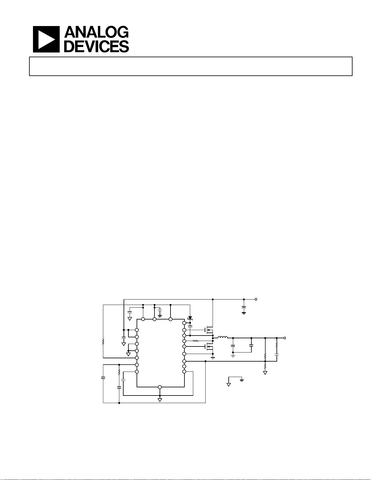
R6
100kΩ
C2
33pF
20kΩ
C3
5.6nF
C5
1µF
VREG
IN
C6
1µF
R8
C
SS
200nF
EN
FREQ
SYNC
PGOOD
COMP
SS
C7
1µF
PV TRK
ADP1828
GND
AGND
CLKOUT
CLKSET
BST
DH
SW
CSL
DL
PGND
FB
Step-Down, DC-to-DC Controller
ADP1828
to regulate an output voltage as low as 0.6 V to 85% of the input
voltage and is sized to handle large MOSFETs for point-of-load
regulators. The ADP1828 is ideal for a wide range of high power
applications, such as DSP and processor core I/O power, and
general-purpose power in telecommunications, medical imaging,
PC, gaming, and industrial applications. It operates from input
bias voltages of 3 V to 18 V with an internal LDO that generates
a 5 V output for input bias voltages greater than 5.5 V.
The ADP1828 operates at a pin-selectable, fixed switching
frequency of either 300 kHz or 600 kHz, or at any frequency
between 300 kHz and 600 kHz with a resistor. The switching
frequency can also be synchronized to an external clock up to
2× the part’s nominal oscillator frequency. The clock output
can be used for synchronizing additional ADP1828s (or the
ADP1829 controllers), thus eliminating the need for an external
clock source. The ADP1828 includes soft start protection to
limit any inrush current from the input supply during startup,
reverse current protection during soft start for a precharged
output, as well as a unique adjustable lossless current-limit
scheme utilizing external MOSFET R
For applications requiring power-supply sequencing, the
ADP1828 provides a tracking input that allows the output
voltage to track during startup, shutdown, and faults. The
additional supervisory and control features include thermal
overload, undervoltage lockout, and power good.
The ADP1828 operates over the −40°C to +125°C junction
temperature range and is available in a 20-lead QSOP.
= 10V TO 18
IN
C
IN
180µF
×2
D1
C4
0.47µF
R
CL
1.8kΩ
M1
L1 = 0.82µH
M2
×2
20V
C
OUT2
1000µF
×2
PGNDAGND
C
OUT1
47µF
X5R
6.3V
OUTPUT
1.8V, 20A
R1
20kΩ
R2
10kΩ
R3
7.5kΩ
C1
680pF
DSON
sensing.
f
= 300kHz
SW
C
: SANYO, O SCON 20SP180M
IN
C
: SANYO, PO SCAP 2R5TPD1000M5
OUT2
L1: WURTH ELEKTRONIC, 0.82µH, 744355182
D1: BAT54
M1: INFINE ON, BSC080N03LS
M2: INFINE ON, 2 × BSC030N03LS
06865-001
Figure 1. Typical Application Circuit with 20 A Output
Rev. 0
Information furnished by Analog Devices is believed to be accurate and reliable. However, no
responsibility is assumed by Analog Devi ces for its use, nor for any infringements of patents or other
rights of third parties that may result from its use. Specifications subject to change without notice. No
license is granted by implication or otherwise under any patent or patent rights of Analog Devices.
Trademarks and registered trademarks are the property of their respective owners.
One Technology Way, P.O. Box 9106, Norwood, MA 02062-9106, U.S.A.
Tel: 781.329.4700 www.analog.com
Fax: 781.461.3113 ©2007 Analog Devices, Inc. All rights reserved.
Page 2

ADP1828
TABLE OF CONTENTS
Features .............................................................................................. 1
Applications ....................................................................................... 1
General Description ......................................................................... 1
Revision History ............................................................................... 2
Specifications ..................................................................................... 3
Absolute Maximum Ratings ............................................................ 6
ESD Caution .................................................................................. 6
Simplified Block Diagram ............................................................... 7
Pin Configuration and Function Descriptions ............................. 8
Typical Performance Characteristics ............................................. 9
Theory of Operation ...................................................................... 14
Input Power ................................................................................. 14
Internal Linear Regulator .......................................................... 14
Soft Start ...................................................................................... 14
Error Amplifier ........................................................................... 15
Current-Limit Scheme ............................................................... 15
MOSFET Drivers ........................................................................ 15
Setting the Output Voltage ........................................................ 16
Switching Frequency Control and Synchronization .............. 16
Compensation ............................................................................. 17
Power-Good Indicator ............................................................... 17
Thermal Shutdown ..................................................................... 17
Shutdown Control ...................................................................... 17
Tracking ....................................................................................... 17
Application Information ................................................................ 18
Selecting the Input Capacitor ................................................... 18
Output LC Filter ......................................................................... 18
Selecting the MOSFETs ............................................................. 19
Setting the Current Limit .......................................................... 20
Accurate Current-Limit Sensing .............................................. 20
Feedback Voltage Divider ......................................................... 20
Compensating the Voltage Mode Buck Regulator ................. 20
Soft Start ...................................................................................... 24
Switching Noise and Overshoot Reduction ............................ 24
Voltage Tracking ......................................................................... 24
Coincident Tracking .................................................................. 25
Ratiometric Tracking ................................................................. 25
Thermal Considerations ............................................................ 27
PCB Layout Guideline ................................................................... 28
Recommended Component Manufacturers ........................... 29
Application Circuits ....................................................................... 30
Outline Dimensions ....................................................................... 32
Ordering Guide .......................................................................... 32
REVISION HISTORY
9/07—Revision 0: Initial Version
Rev. 0 | Page 2 of 32
Page 3

ADP1828
SPECIFICATIONS
IN = 12 V, PV = VEN = V
lation using standard statistical quality control (SQC). T
Table 1.
Parameter Conditions Min Typ Max Unit
POWER SUPPLY
IN Input Voltage PV is tied to VREG, IN is not tied to VREG (using internal regulator) 5.5 18 V
IN Input Voltage IN = PV = VREG, IN is tied to VREG (not using internal regulator) 3.0 5.5 V
IN Quiescent Current Not switching, I
IN Shutdown Current EN = GND 5 15 A
VREG-to-GND Shutdown Impedance EN = GND, IN is not tied to VREG 1.6 MΩ
VREG Undervoltage Lockout Threshold VREG rising 2.4 2.7 3.0 V
VREG Undervoltage Lockout Hysteresis VREG falling 0.125 V
ERROR AMPLIFER
FB Regulation Voltage TA = 25°C, TRK > 700 mV 597 600 603 mV
T
T
FB Input Bias Current 5 100 nA
Open-Loop Voltage Gain 70 dB
Gain-Bandwidth Product 20 MHz
COMP Sink Current 600 µA
COMP Source Current 120 µA
COMP Clamp High Voltage IN = VREG = 3V 2.4 V
IN = 12 V 3.6 V
COMP Clamp Low Voltage 0.75 V
LINEAR REGULATOR
VREG Output Voltage
VREG Load Regulation I
VREG Line Regulation IN = 5 V+ dropout voltage to 18 V, no load 1 mV
VREG Current Limit VREG drops to 4 V 220 mA
VREG Short-Circuit Current VREG drops to 0.4 V 60 140 200 mA
IN to VREG Dropout Voltage
VREG Minimum Output Capacitance 1 F
PWM CONTROLLER
VRAMP Peak-to-Peak Voltage
DH Maximum Duty Cycle FREQ = GND (300 kHz) 91 93 %
DH Minimum On Time Any frequency 100 ns
DL Minimum On Time Any frequency 200 ns
SOFT START
SS Pull-Up Resistance SS = GND 90 kΩ
SS Pull-Down Resistance SS = 0.6 V 6 kΩ
SS to FB Offset Voltage SS = 0 mV to 500 mV −45 mV
SS Pull-Up Voltage 0.8 V
TRACKING
TRK Common-Mode Input Voltage Range 0 600 mV
TRK to FB Offset Voltage TRK = 0 mV to 500 mV −5.5 +5 mV
TRK Input Bias Current 100 nA
= 5 V, SYNC = GND, unless otherwise specified. All limits at temperature extremes are guaranteed via corre-
TRK
= −40°C to +125°C, unless otherwise specified. Typical values are at TA = 25°C.
J
= 0 mA 1.5 3.0 mA
VREG
= 0°C to +70°C, TRK > 700 mV 595 605 mV
A
= −40°C to +125°C, TRK > 700 mV 591 609 mV
J
IN = 5 V+ dropout voltage to 18 V, I
= −40°C to +125°C
T
J
= 0 mA to 100 mA, IN = 5.25 V to 18 V −10 mV
VREG
1
2
I
= 100 mA, IN < 5 V 0.6 1.0 V
VREG
0.7 1.0 1.45 V
=100 mA
VREG
4.75 5.0 5.25 V
Rev. 0 | Page 3 of 32
Page 4

ADP1828
Parameter Conditions Min Typ Max Unit
OSCILLATOR
Oscillator Frequency SYNC = FREQ = GND 240 300 360 kHz
SYNC = GND, FREQ = VREG 480 600 720 kHz
R
R
R
SYNC Synchronization Range FREQ = GND 300 600 kHz
FREQ = VREG 600 1200 kHz
SYNC Input Pulse Width 200 ns
SYNC Pin Capacitance 5 pF
CURRENT SENSE
CSL Threshold Voltage Relative to PGND −17 −38 −58 mV
CSL Output Current CSL = PGND 42 50 56 A
Current Sense Blanking Period 100 ns
GATE DRIVERS
DH Rise Time CDH = 3 nF, V
DH Fall Time CDH = 3 nF, V
DL Rise Time CDL = 3 nF 15 ns
DL Fall Time CDL = 3 nF 10 ns
DH or DL Driver RON, Sourcing Current
DH or DL Driver RON, Sinking Current
3, 4
3, 4
Sinking 1.5 A with a 0.1 µs pulse 1.5 Ω
DH or DL Driver RON, Sourcing Current IN = VREG = 3 V; sourcing 1 A with a 0.1 µs pulse 2.3 Ω
DH or DL Driver RON, Sinking Current IN = VREG = 3 V; sinking 1 A with a 0.1 µs pulse 2 Ω
DH to DL, DL to DH Dead Time 40 ns
CLOCK OUT
CLOCKOUT Pulse Width 360 ns
CLKOUT Rise or Fall Time C
SYNC to CLKOUT Propagation Delay, tPD C
SYNC to CLKOUT Propagation Delay, tPD C
LOGIC THRESHOLDS
SYNC, CLKSET, FREQ Logic High 1.8 V
SYNC, CLKSET Logic Low 0.4 V
FREQ Logic Low 0.25 V
CLKSET, SYNC, FREQ Input Leakage
Current
EN Input Threshold 1.1 1.5 1.8 V
EN Input Threshold Hysteresis 0.2 V
EN Current Source EN = 0 V to 3.0 V −0.1 −0.6 −1.5 A
EN Input Impedance to 5 V Zener EN = 5.5 V to 18 V 100 kΩ
THERMAL SHUTDOWN
Thermal Shutdown Threshold
4
Thermal Shutdown Hysteresis4 15 °C
= 57.6 kΩ 240 300 360 kHz
FREQ
= 35.7 kΩ 370 450 530 kHz
FREQ
= 24.9 kΩ 480 600 720 kHz
FREQ
− VSW = 5 V 15 ns
BST
− VSW = 5 V 10 ns
BST
Sourcing 1.5 A with a 0.1 µs pulse 2 Ω
= 47 pF 10 ns
CLKOUT
CLKOUT
CLKOUT
= 47 pF, C
= 47 pF, C
= 5 pF 40 ns
SYNC
= 5 pF, IN < 5 V 52 ns
SYNC
CLKSET, SYNC, FREQ = 0 V or VREG 1 A
145 °C
Rev. 0 | Page 4 of 32
Page 5

ADP1828
Parameter Conditions Min Typ Max Unit
POWER GOOD
FB Overvoltage Threshold VFB rising 700 750 810 mV
FB Overvoltage Hysteresis 50 mV
FB Undervoltage Threshold VFB falling 500 550 585 mV
FB Undervoltage Hysteresis 50 mV
PGOOD Propagation Delay 8 s
PGOOD Off Leakage Current V
PGOOD Output Low Voltage I
1
Connect IN to VREG when IN < 5.5 V. For applications with IN < 5.5V and IN not connected to VREG, keep in mind that VREG = VIN – dropout. VREG needs to be ≥ 3 V for
proper operation.
2
V
= 1.0 V × f
RAMP
then fSW = f
3
With a 5 V drive, the peak source or sink current could be up to 2.5 A and 3.3 A, respectively, when driving external power MOSFETs. The duration of the peak current
pulse is generally in the order of 10 ns.
4
Guaranteed by design and characterization. Not subject to production test.
SYNC
OSC/fSW
.
, where f
is the natural oscillator frequency and fSW is the actual switching frequency. If SYNC is not used, then f
OSC
= 5.5 V 1 A
PGOOD
= 10 mA 150 500 mV
PGOOD
= fSW. If SYNC is used,
OSC
Rev. 0 | Page 5 of 32
Page 6
ADP1828
ABSOLUTE MAXIMUM RATINGS
Table 2.
Parameter Rating
IN, TRK −0.3 V to +20 V
EN −0.3 V < IN + 0.3 V
PV, SYNC, FREQ, COMP, SS, FB, PGOOD,
−0.3 V to +6 V
CLKSET, CLKOUT, VREG
BST-to-GND, SW-to-GND −0.3 V to +30 V
BST-to-SW −0.3 V to +6 V
BST-to-GND, SW-to-GND, 50 ns transients +38 V
SW-to-GND, 30 ns negative transients −7 V
CSL-to-GND −1 V to +30 V
DH-to-GND
(SW − 0.3 V) to
(BST + 0.3 V)
DL-to-PGND
−0.3 V to
(PV + 0.3 V)
PGND-to-GND ±2 V
θJA, 20-Lead QSOP on a Multilayer PCB
(Natural Convection)
1
83°C/W
Operating Junction Temperature2 −40°C to +125°C
Storage Temperature −65°C to +150°C
Maximum Soldering Lead Temperature 260°C
1
Junction-to-ambient thermal resistance (θJA) of the package was calculated
or simulated on a multilayer PCB.
2
The ADP1828 can be damaged when the junction temperature limits are
exceeded. Monitoring ambient temperature does not guarantee that TJ
is within the specified temperature limits. In applications with moderate
power dissipation and low PCB thermal resistance, the maximum ambient
temperature can exceed the maximum limit as long as the junction temperature is within specification limits. The junction temperature, TJ, of the
device is dependent on the ambient temperature, TA, the power dissipation
of the device, PD, and the junction to ambient thermal resistance of the
package, θJA. Maximum junction temperature is calculated from the ambient
temperature and power dissipation using the formula TJ = TA + PD × θJA.
Stresses above those listed under Absolute Maximum Ratings
may cause permanent damage to the device. This is a stress
rating only; functional operation of the device at these or any
other conditions above those indicated in the operational
section of this specification is not implied. Exposure to absolute
maximum rating conditions for extended periods may affect
device reliability.
Absolute maximum ratings apply individually only, not in
combination. Unless otherwise specified all other voltages
are referenced to GND.
ESD CAUTION
Rev. 0 | Page 6 of 32
Page 7
ADP1828
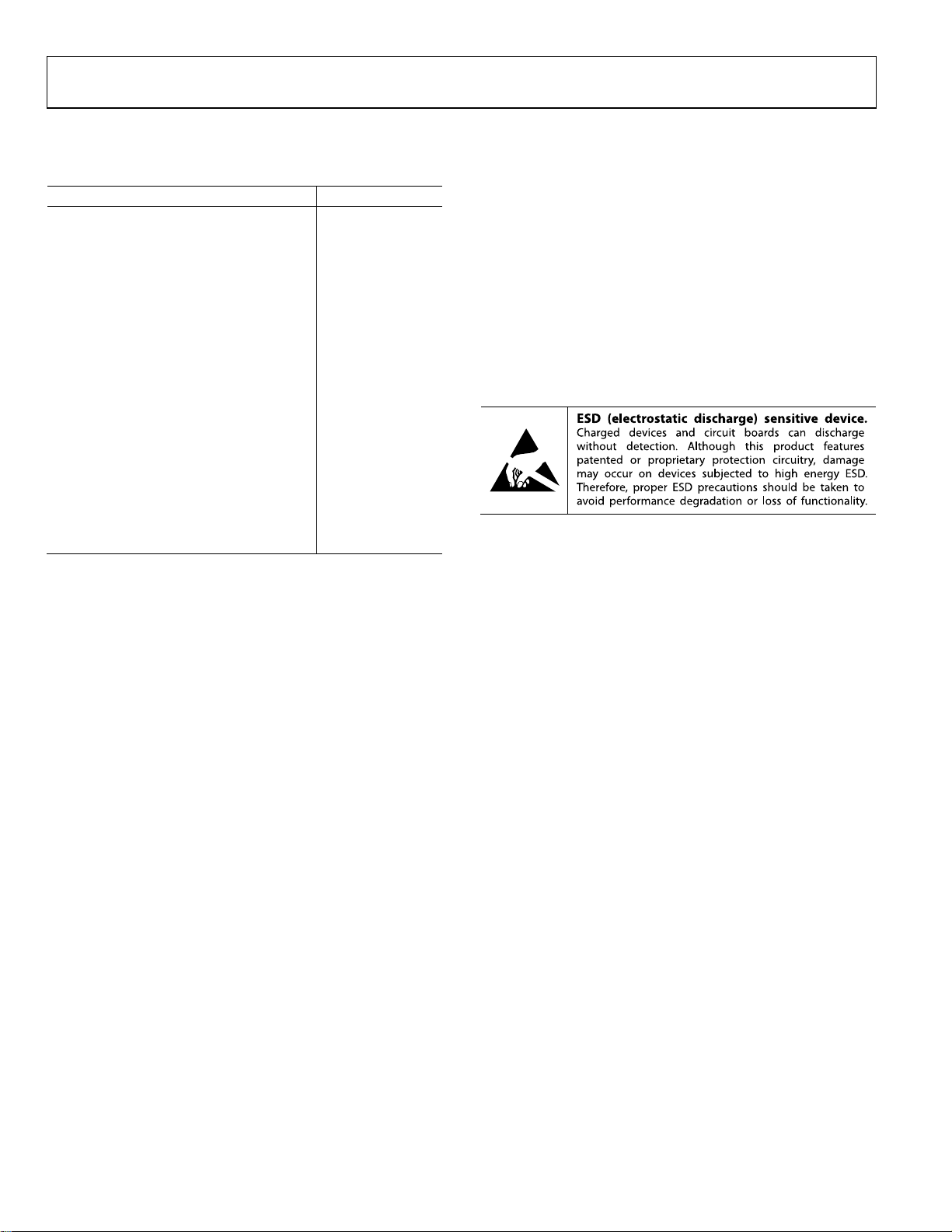
SIMPLIFIED BLOCK DIAGRAM
IN
ADP1828
VREG
0.6V
0.8V
REF
0.75V
0.55V
UVLO
IN
LINEAR
REG
THERMAL
SHUTDOWN
EN
CLKOUT
CLKSET
FREQ
SYNC
COMP
FB
TRK
SS
GND
100kΩ
CLKOUT
DRIVER
OSCILLAT OR
90kΩ
6kΩ
0.6V
RAMP
CLK
0.8V
FAULT
FAULT
PWM
COMPARATOR
0.75V
ERROR
AMPLIFIER
0.55V
Figure 2. Simplified Block Diagram
LOGIC
50µA
VREG
R
ILIM
PWM
BST
DH
QS
Q
SW
PV
DL
PGND
CSL
PGOOD
06865-003
Rev. 0 | Page 7 of 32
Page 8
ADP1828
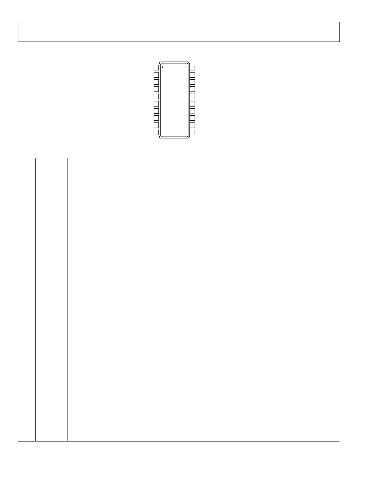
PIN CONFIGURATION AND FUNCTION DESCRIPTIONS
FREQ
SYNC
EN
VREG
GND
COMP
FB
TRK
SS
IN
1
2
3
ADP1828
4
TOP VIEW
5
(Not to Scale)
6
7
8
9
10
20
19
18
17
16
15
14
13
12
11
CLKOUT
CLKSET
BST
DH
SW
CSL
PGND
DL
PV
PGOOD
06865-004
Figure 3. Pin Configuration
Table 3. Pin Function Descriptions
Pin
No.
Mnemonic Description
1 FREQ
Frequency Control Input. Low for 300 kHz, high for 600 kHz, or connect a resistor from FREQ to GND to set the freerunning frequency between 300 kHz and 600 kHz.
2 SYNC
Frequency Synchronization Input. Accepts external signals between 300 kHz and 600 kHz if FREQ is set to low, or
between 600 kHz and 1.2 MHz if FREQ is set to high. If f
from f
up to 600 kHz. If SYNC is not used, connect SYNC to GND or VREG. V
OSC
is set by R
OSC
, then the synchronization frequency range is
FREQ
can be driven up to 6 V even when VIN
SYNC
is less than 6 V.
3 EN
Enable Input. Drive EN high or tristate EN to turn on the ADP1828 controller, and drive it low to turn off. Connect EN to
IN for automatic startup.
4 IN
Input Supply to the Internal Linear Regulator. Drive IN with 5.5 V to 18 V to power the ADP1828 from LDO, VREG; tie PV
to VREG. For input voltages between 3 V and 5.5 V, tie IN, PV, and VREG together.
5 VREG
Output of the Internal Linear Regulator (LDO). The internal circuitry and gate drivers are powered from VREG. Bypass
VREG to AGND plane with 1 F ceramic capacitor for stable operation, for example, a 10 V X5R 1 F ceramic capacitor
is sufficient. The VREG output is 5 V when IN = 5 V + dropout. Connect IN to VREG and PV when IN = 3 V to 5.5 V. For
applications with IN < 5.5 V and IN not connected to VREG, keep in mind that VREG = VIN – dropout. VREG needs to be
≥3 V for proper operation.
6 GND Ground for Internal Circuits. Tie the bottom of the feedback dividers to this GND.
7 COMP Error Amplifier Output. Connect an RC network from COMP to FB for loop compensation.
8 FB
Voltage Feedback. Connect a resistor divider from the buck regulator output to GND and tie the tap to FB to set the
output voltage.
9 TRK
Tracking Input. To track a master voltage, drive TRK from a voltage divider from the master voltage. If the tracking
function is not used, connect TRK to VREG.
10 SS Soft Start Control Input. Connect a capacitor from SS to GND to set the soft start period.
11 PGOOD
Open-Drain Power-Good Output. Sinks current when FB is out of regulation. Connect a pull-up resistor from
PGOOD to VREG.
12 PV
Positive Input Voltage for Gate Driver DL. When IN is 3 V to 5.5 V, connect IN to VREG and PV. Connect a 1 F bypass
capacitor from PV to PGND. When IN = 5.5 V to 18 V, connect PV to VREG.
13 DL Low-Side (Synchronous Rectifier) Gate Driver Output.
14 PGND Power GND. Ground for gate driver.
15 CSL Current Sense Comparator Inverting Input. Connect a resistor between CSL and SW to set the current-limit offset.
16 SW Switch Node Connection.
17 DH High-Side (Switch) Gate Driver Output.
18 BST
Boost Capacitor Input. Powers the high-side gate driver DH. Connect a 0.22 F to 0.47 F ceramic capacitor from BST
to SW and a Schottky diode from PV to BST.
19 CLKSET
Clock Set Input. Setting CLKSET to Logic high (connect CLKSET to VREG) sets the CLKOUT to 2× the internal oscillator
frequency and is in phase with the oscillator. Setting CLKSET to Logic low sets the CLKOUT to 1× the oscillator
frequency and 180° out of phase.
20 CLKOUT
Clock Output. The CLKOUT frequency, f
synchronize another ADP1828 or ADP1829 controllers. Set f
2× when synchronizing the ADP1829. If SYNC is used, f
, is either 1× or 2× the oscillator frequency. CLKOUT can be used to
CLKOUT
SYNC
to 1× when synchronizing another ADP1828, or to
CLKOUT
= f
independent of the CLKSET voltage. CLKOUT is
CLKOUT
able to drive a 100 pF load.
Rev. 0 | Page 8 of 32
Page 9
ADP1828
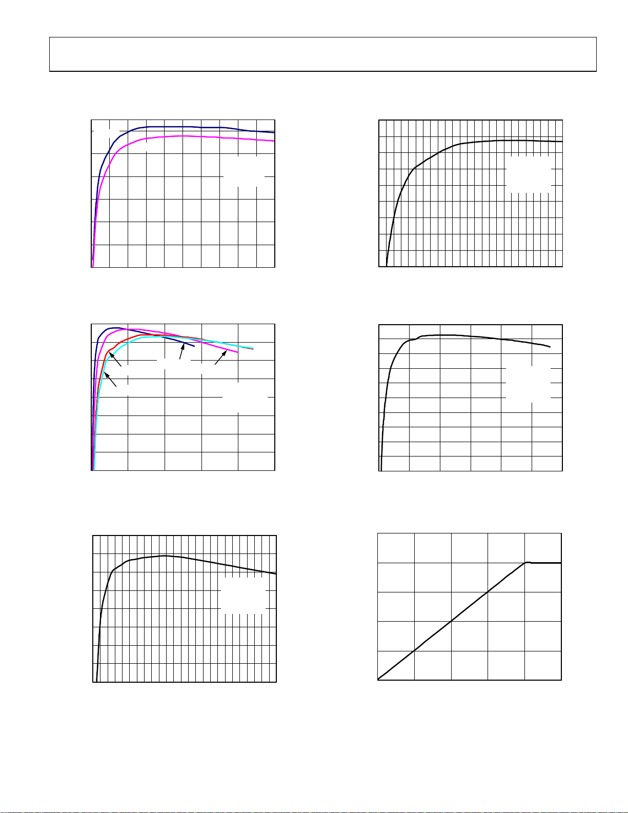
TYPICAL PERFORMANCE CHARACTERISTICS
95
90
300kHz
80
70
60
EFFICIENCY (%)
50
40
30
02468101214161820
600kHz
LOAD (A)
VIN = 12V
= 1.8V
V
OUT
= 25°C
T
A
Figure 4. Efficiency vs. Load Current of Figure 1
06865-002
90
85
80
75
70
EFFICIENCY (%)
65
60
55
50
0123 45
LOAD (A)
fSW = 600kHz
= 12V
V
IN
= 3.3V
V
OUT
= 25°C
T
A
Figure 7. Efficiency vs. Load Current of Figure 54
06865-007
95
90
85
VIN = 12V
80
VIN = 15V
75
70
EFFICIENCY (%)
65
60
55
0 5 10 15 20 25
VIN = 3.3V
LOAD (A)
VIN = 5.5V
f
SW
V
OUT
T
A
= 25°C
= 300kHz
= 1.8V
Figure 5. Efficiency vs. Load Current of Figure 1
95
90
85
80
75
70
EFFICIENCY (%)
65
60
55
012345
LOAD (A)
fSW = 600kHz
= 3.3V
V
IN
= 1.2V
V
OUT
= 25°C
T
A
Figure 6. Efficiency vs. Load Current of Figure 53
95
90
85
80
75
70
65
EFFICIENCY (%)
60
55
50
45
06865-005
0 5 10 15 20 25 30
LOAD (A)
fSW = 300kHz
V
= 12V
IN
V
= 1.8V
OUT
T
= 25°C
A
06865-008
Figure 8. Efficiency vs. Load Current of Figure 56
5.5
T
= 25°C
A
5.0
4.5
4.0
VREG OUTPUT (V)
3.5
3.0
3.0 3.5 4.0 4.5 5.0 5.5
06865-006
V
(V)
IN
06865-009
Figure 9. VREG in Dropout, No Load
Rev. 0 | Page 9 of 32
Page 10
ADP1828
5.000
4.995
4.990
4.985
4.980
4.975
4.970
VREG OUTPUT (V)
4.965
4.960
4.955
4.950
0 20 40 60 80 100
VREG LOAD CURRENT (mA)
Figure 10. VREG vs. Load Current
5.000
VIN = 7V
4.995
4.990
4.985
4.980
4.975
VREG (V)
4.970
4.965
4.960
4.955
4.950
–50 –25 0 25 50 75 100 125
TEMPERATURE ( °C)
NO LOAD
10mA LOAD
100mA LOAD
Figure 11. VREG Voltage vs. Temperature
VIN = 5.5V
T
= 25°C
A
3.0
2.5
2.0
(%)
1.5
OSC
f
Δ
1.0
0.5
0
06865-010
3 5 7 9 11 13 15 17
Figure 13. Δ f
1
2
06865-011
CH1 5.00V CH2 100mV M 400ns A CH1 3. 60V
B
W
600kHz
300kHz
V
(V)
IN
vs. VIN, Referenced at VIN = 3 V
OSC
T
SW
VREG (AC-COUPLED)
B
W
TA = 25°C
VIN = 5.5V
LOAD = 5A
06865-013
06865-014
Figure 14. VREG Output of Figure 54
5
4
3
2
VREG OUTPUT (V)
1
0
0 50 100 150 200 250
VREG LOAD CURRENT (mA)
VIN = 5.5V
T
= 25°C
A
Figure 12. VREG Current-Limit Foldback
06865-012
Rev. 0 | Page 10 of 32
0.6025
0.6020
0.6015
0.6010
0.6005
0.6000
FEEDBACK VOLTAGE (V)
0.5995
0.5990
–40 –15 10 35 60 85 110 135
TEMPERATURE ( °C)
Figure 15. Feedback Voltage vs. Temperature, VIN = 12 V
06865-015
Page 11

ADP1828
2.0
VIN = 3V TO 18V
f
1.5
= 300kHz OR 600kHz
OSC
REFERENCE POI NT IS AT 25°C
1.0
0.5
(kHz)
0
OSC
Δf
–0.5
–1.0
–1.5
–2.0
–50 –25 0 25 50 75 100 125 150
TEMPERATURE ( °C)
Figure 16. Δ f
vs. Temperature
OSC
6
TA = 25°C
5
4
3
2
QUIESCENT CURRE NT (mA)
1
0
2 5 8 11141720
V
(V)
IN
Figure 17. Supply Current vs. Input Voltage
T
V
(AC-COUPLED)
OUT
1
STEP LOAD (5A TO 20A)
4
06865-016
CH1 100mV
B
W
CH4 5.00A Ω
M 200µs A CH4 8.20A
06865-019
Figure 19. Load Transient Response of Figure 1, 5 A to 20 A, VIN = 12 V
T
SW
1
2
INPUT RIPPLE
3
OUTPUT RI PPLE
06865-017
CH1 10.0V
CH3 10.0mV
CH2 50.0mV M 1.00µs A CH1 5. 80V
B
W
B
W
06865-020
Figure 20. Input and Output Ripple of Figure 54, 4 A Load
T
SW
1
INPUT RIPPLE
2
OUTPUT RI PPLE
3
CH1 10.0V
CH3 50.0mV
B
CH2 5.00V M 1.00µs A CH1 6.40V
W
B
W
B
W
Figure 18. Input and Output Ripple of Figure 1, 22 A Load
06865-018
Rev. 0 | Page 11 of 32
T
INPUT VOL TAGE (AC-CO UPLED)
2
3
4
CH3 100mV
OUTPUT (AC-CO UPLED)
STEP LO AD (1A TO 5A)
CH2 200mV
B
CH4 5.00A Ω
W
B
M 200µs A CH4 4.20A
W
06865-021
Figure 21. Load Transient Response of Figure 54, 1 A to 5 A, VIN = 12 V
Page 12

ADP1828
T
VIN = 5V TO 9V TO 5V
1
3
CH1 2.00V
CH3 50.0mV
V
(AC-COUPLED)
OUT
B
W
M 4.00ms A CH1 6.08V
Figure 22. Line Transient Response of Figure 1, No Load
SHORT CIRCUI T APPLIED
1
SS
2
V
OUT
3
SHORT CIRCUI T REMOVED
VIN = 5.5V
T
V
1
IN
SS
2
V
3
OUT
SW
4
CH1 5.00V
06865-022
CH3 1.00V
CH2 500mV M 2.00ms A CH1 4.10V
B
CH4 5.00V
W
B
W
06865-025
Figure 25. Power-On Response, EN Tied to VIN
T
TRK
FB
4
CH1 5.00V
CH3 1.00V
CH2 500mV M 20.0ms A CH3 1.34V
B
CH4 5.00A Ω
W
INPUT CURRENT
B
W
Figure 23. Output Short-Circuit Response
T
EN
1
V
OUT
2
3
CH1 5.00V
CH3 1. 00V
SS
CH2 1.00V M 4.00ms A CH1 3. 000V
B
W
B
W
Figure 24. Soft Start and Inrush Current of Figure 1
1
06865-023
CH1 200mV CH2 200mV M 20.0ms A CH1 680mV
B
W
B
W
06865-026
Figure 26. Tracking, TRK from 0 V to 1 V
T
TRK AND FB SUPERIMPOSED
1
06865-024
CH1 100mV CH2 100mV M 20.0ms A CH1 352mV
B
W
B
W
06865-027
Figure 27. Tracking, TRK from 0 V to 0.5 V
Rev. 0 | Page 12 of 32
Page 13

ADP1828
2
3
4
CH3 5.00V CH4 5.00V
CH2 10.0V M 1.00µs A CH2 4.80V
Figure 28. CLKOUT, CLKSET = 0 V Figure 31. Start into Precharged Output
2
3
DH
DL
CLKOUT
T
T
T
DH
1
FB
2
SS
VIN = 0V TO 3V
VREG
4
CH1 5.00V
06865-029
CH3 200mV
B
CH2 200mV M 4.00ms A CH4 1.12V
W
B
CH4 2.00V
W
B
W
B
W
06865-032
T
EN
DH
1
DL
2
DH
4
CH3 5.00V CH4 5.00V
CH2 10.0V M 1.00µs A CH2 4.80V
CLKOUT
3
CH1 5.00V
06865-030
CH3 5.00V
B
CH2 10.0V M 4.00µs A CH2 8.20V
W
B
W
DL
B
W
06865-033
Figure 29. CLKOUT, CLKSET = 5 V Figure 32. EN, Shutdown
T
SYNC
1
DH
2
DL
3
CLKOUT
4
CH3 5.00V CH4 5.00V
CH2 10.0VCH1 5.00V M 1.00µs A CH1 3.50V
06865-031
Figure 30. SYNC
Rev. 0 | Page 13 of 32
Page 14

ADP1828
THEORY OF OPERATION
The ADP1828 is a versatile, synchronous-rectified, fixedfrequency, pulse-width modulation (PWM), voltage mode,
step-down controller capable of generating an output voltage
as low as 0.6 V to 85% of the input voltage. It is ideal for a wide
range of applications, such as DSP and processor core I/O supplies,
general-purpose power in telecom, medical imaging, gaming,
PCs, set-top boxes, and industrial controls. The ADP1828
controller operates directly from 3 V to 18 V. It includes fully
integrated MOSFET gate drivers and a linear regulator for
internal and gate drive bias.
The ADP1828 operates at a pin-selectable, fixed switching
frequency of either 300 kHz or 600 kHz, or operates at any
frequency between 300 kHz and 600 kHz by connecting a
resistor between FREQ and GND. The switching frequency
can also be synchronized to an external clock up to 2× the
part’s nominal oscillator frequency. The built-in clock output
can be used for synchronizing the ADP1829 and other ADP1828
controllers, thus eliminating the need for an external clock
source. The ADP1828 also includes clockout, voltage tracking,
thermal overload protection, undervoltage lockout, power
good, soft start to limit inrush current from the input supply
during startup, reverse current protection during soft start for
precharged outputs, and an adjustable lossless current-limit
scheme utilizing external MOSFET R
operates over the −40°C to +125°C junction temperature range
and is available in a 20-lead QSOP.
sensing. The ADP1828
DSON
INPUT POWER
The ADP1828 is powered from the IN pin from 3.0 V up to
18 V. The internal low dropout linear regulator, regulates the
IN voltage down to 5 V when IN is between 5.5 V and 18 V.
The output of the LDO is denoted as VREG. The control circuits,
gate drivers, and the external boost capacitor operate from the
LDO output for IN between 5.5 V and 18 V. PV powers the
low-side MOSFET gate drive (DL), and IN powers the internal
control circuitry. Bypass PV to PGND with a 1 F or greater
capacitor, and bypass IN to GND with a 0.1 F or greater
capacitor. Bypass the power input to PGND with a suitably
large capacitor.
The VREG output is sensed by the undervoltage lock-out
(UVLO) circuit to be certain that enough voltage headroom
is available to run the controllers and gate drivers. As VREG
rises above about 2.7 V, the controllers are enabled. The IN
voltage is not directly monitored by the UVLO circuit. If the
IN voltage is insufficient to allow VREG to be above the
UVLO threshold, the controllers are disabled, but the LDO
continues to operate. The LDO is enabled and cannot be
turned off whenever EN is high, even if VREG is below the
UVLO threshold.
For a supply voltage between 5.5 V and 18 V, connect IN to the
supply voltage, and tie VREG to PV. For a supply voltage between
3 V and 5.5 V, connect IN, PV, and VREG to the supply voltage.
In this case, the input supply voltage directly powers the lowside gate driver.
While IN is limited to 18 V, the switching stage can run from
up to 24 V and the BST pin can go to 30 V to support the gate
drive. This can provide an advantage, for example, in the case
of high frequency operation from high input voltage. Power
dissipation in the ADP1828 can be limited by running IN from
a low voltage rail while operating the switches from the high
voltage rail.
INTERNAL LINEAR REGULATOR
The internal linear regulator has low dropout, meaning it can
regulate its output voltage (VREG) close to the input voltage.
It powers up the internal control circuitry and provides bias
for the gate drivers when VREG is tied to PV. It is guaranteed
to have more than 100 mA of output current capability, which
is sufficient to handle the gate drive requirements of typical
logic threshold MOSFETs driven at up to 1.2 MHz. Bypass
VREG to AGND with a 1 µF or greater capacitor.
Because the LDO supplies the gate drive current, the output
of VREG is subjected to sharp transient currents as the drivers
switch and the boost capacitors recharge during each switching
cycle. The LDO has been optimized to handle these transients
without overload faults. Due to the gate drive loading, using
the VREG output for other auxiliary system loads is not
recommended.
The LDO includes a current limit well above the expected
maximum gate drive load. This current limit also includes a
short-circuit fold back to further limit the VREG current in
the event of a short-circuit fault.
SOFT START
The ADP1828 employs a programmable soft start that reduces
input current transients and prevents output overshoot. SS drives
an auxiliary positive input to the error amplifier; thus, the voltage
at this pin regulates the voltage at the feedback control pin.
Program the soft start by connecting a capacitor from SS to
GND. On startup, the capacitor charges from an internal
90 kΩ resistor to 0.8 V. The dc-to-dc converter output voltage
rises with the voltage at the soft start pin, allowing the output
voltage to rise slowly and reducing the inrush current.
Rev. 0 | Page 14 of 32
Page 15

ADP1828
If the output voltage is precharged prior to turn-on, the ADP1828
prevents reverse inductor current, which would discharge the
output capacitor. Once the voltage at SS exceeds the regulation
voltage (typically 0.6 V), the reverse current is re-enabled to
allow the output voltage regulation to be independent of load
current.
When a controller is disabled or experiences any form of fault
condition, the soft start capacitor is discharged through an
internal 6 k resistor, so that at restart or recovery from fault
the output voltage soft starts again.
ERROR AMPLIFIER
The ADP1828 error amplifier is an operational amplifier. The
ADP1828 senses the output voltage through an external resistor
divider at the FB pin. The FB pin is the inverting input to the
error amplifier. The error amplifier compares this feedback
voltage to the internal 0.6 V reference, and the output of the
error amplifier appears at the COMP pin. The COMP pin
voltage then directly controls the duty cycle of the switching
converter.
A series/parallel RC network is tied between the FB pin and the
COMP pin to provide the compensation for the buck converter
control loop. A detailed design procedure for compensating the
system is provided in the Compensating the Voltage Mode Buck
Regulator section.
The error amplifier output is clamped between a lower limit of
about 0.75 V and a higher limit of up to about 3.6 V, depending
on the VREG voltage. When the COMP pin is low, the switching
duty cycle goes to 0%, and when the COMP pin is high, the
switching duty cycle goes to the maximum.
The SS and TRK pins are auxiliary positive inputs to the error
amplifier. Whichever voltage is lowest (SS, TRK, or the internal
0.6 V reference) controls the FB pin voltage and the output. As
a consequence, if two of these inputs are close to each other, a
small offset is imposed on the error amplifier.
CURRENT-LIMIT SCHEME
The ADP1828 employs a programmable, cycle-by-cycle lossless
current-limit circuit that uses an inexpensive resistor to set the
threshold. Every switching cycle, the synchronous rectifier
turns on for a minimum time and the voltage drop across
the MOSFET R
is too high.
This measurement is done by an internal current-limit comparator and an external current-limit setting resistor. The resistor
is connected between the switch node (that is the drain of the
rectifier MOSFET) and the CSL pin. The CSL pin, which is the
inverting input of the comparator, forces 50 A through the
resistor to create an offset voltage drop across it.
When the inductor current is flowing in the MOSFET rectifier,
its drain is forced below PGND by the voltage drop across its
R
. If the R
DSON
is measured to determine if the current
DSON
voltage drop exceeds the preset drop on
DSON
the current-limit resistor, the inverting comparator input is
similarly forced below PGND and an overcurrent fault is
flagged.
The normal transient ringing on the switch node is ignored
for 100 ns after the synchronous rectifier turns on, so the overcurrent condition must also persist for 100 ns for a fault to be
flagged.
When the ADP1828 senses an overcurrent condition, the next
switching cycle is suppressed, the soft start capacitor is discharged
through an internal 6 k resistor, and the error amplifier output
voltage is pulled down. The ADP1828 remains in this mode for
as long as the overcurrent condition persists.
Note that the current-limit scheme in the ADP1828 is not the
same as a short-circuit protection. The ADP1828 does not go
into current foldback in the event of a short circuit. The shortcircuit output current is the current limit set by the R
resistor
CL
and is monitored cycle by cycle. When the overcurrent condition
is removed, operation resumes in soft start mode.
MOSFET DRIVERS
The DH pin drives the high-side switch MOSFET. This is a
boosted 5 V gate driver that is powered by a bootstrap capacitor
circuit. This configuration allows the high-side, N-channel
MOSFET gate to be driven above the input voltage, allowing
full enhancement and a low voltage drop across the MOSFET.
The bootstrap capacitor is connected from the SW pin to the
BST pin. A bootstrap Schottky diode connected from the PV
pin to the BST pin recharges the boost capacitor every time the
SW node goes low. Use a bootstrap capacitor value greater than
100× the high-side MOSFET input capacitance.
In practice, the switch node can run up to 24 V of input voltage,
and the boost nodes can operate more than 5 V above this to
allow full gate drive. The IN pin can be run from 3 V to 18 V.
The switching cycle is initiated by the internal clock signal. The
high-side MOSFET is turned on by the DH driver, and the SW
node goes high, pulling up on the inductor. When the internally
generated ramp signal crosses the COMP pin voltage, the switch
MOSFET is turned off and the low-side synchronous rectifier
MOSFET is turned on by the DL driver. Active break-beforemake circuitry as well as a supplemental fixed dead time are
used to prevent cross-conduction in the switches.
The DL pin provides the gate drive for the low-side MOSFET
synchronous rectifier. Internal circuitry monitors the external
MOSFETs to ensure break-before-make switching to prevent
cross-conduction. An active dead-time reduction circuit
reduces the break-before-make time of the switch to limit the
losses due to current flowing through the synchronous rectifier
body diode.
Rev. 0 | Page 15 of 32
Page 16

ADP1828
The PV pin provides power to the low-side drivers. It is limited
to 5.5 V maximum input and should have a local decoupling
capacitor to PGND.
The synchronous rectifier is turned on for a minimum time
of about 200 ns on every switching cycle in order to sense the
current. This minimum off-time plus the nonoverlap dead time
puts a limit on the maximum high-side switch duty cycle based
on the selected switching frequency. Typically, this maximum
duty cycle is about 90% at 300 kHz switching. At 1.2 MHz
switching, it reduces to about 70% maximum duty cycle.
SETTING THE OUTPUT VOLTAGE
The output voltage is set using a resistive voltage divider from
the output to FB. The voltage divider splits the output voltage
to the 0.6 V FB regulation voltage to set the regulation output
voltage. The output voltage can be set to as low as 0.6 V and as
high as 85% of the power input voltage.
SWITCHING FREQUENCY CONTROL AND SYNCHRONIZATION
The ADP1828 has a logic controlled frequency select input,
FREQ, which sets the switching frequency to 300 kHz or
600 kHz. Drive FREQ low at 300 kHz and high at 600 kHz.
The frequency can also be set to between 300 kHz and 600 kHz
by connecting a resistor between FREQ and GND. A 24.9 kΩ
sets the frequency to 600 kHz, 35.7 kΩ to 450 kHz, and 57.6 kΩ
to 300 kHz. Figure 33 shows f
600
550
500
as a function of R
OSC
FREQ
T
= 25°C
A
.
with f
channel ADP1829 controller (see Tab l e 4).
Table 4. CLKOUT Truth Table
EN CLKSET SYNC CLKOUT Comment
H L H/L 1× f
H H H/L 2× f
H X Clock in Clock
L X X L CLKOUT is low
1
To synchronize the ADP1828 switching frequency to an
external signal, drive the SYNC input with an external clock
or with the CLKOUT signal from another ADP1828. The
ADP1828 can be synchronized to between 1× and 2× the
internal oscillator frequency. If f
synchronization frequency range is from f
Driving SYNC faster than recommended for the FREQ setting
results in a small ramp signal, which could affect the signal-tonoise ratio and the modulator gain and stability.
When an external clock is detected at the first SYNC edge, the
internal oscillator is reset and the clock control shifts to SYNC.
The SYNC edges then trigger subsequent clocking of the PWM
outputs. The high-side MOSFET turn-on follows the rising edge
of the sync input by approximately 320 ns (see Figure 34 for
an illustration). If the external SYNC signal disappears during
operation, the ADP1828 reverts to its internal oscillator and
experiences a delay of no more than a single cycle of the
internal oscillator.
. The 2× output is suitable for synchronizing the dual
OSC
1
180° out of phase with f
OSC
In phase with f
OSC
CLKOUT in-sync with
clock in
X: don’t care, H: Logic high, L: Logic low.
is set by R
OSC
OSC
OSC
, then the
FREQ
up to 600 kHz.
OSC
450
400
350
300
OSCILLATOR FREQUENCY (kHz)
250
200
24000 29000 34000 39000 44000 49000 54000 59000
Figure 33. f
R
FREQ
OSC
VIN = 3V
VIN = 5V
(Ω)
vs. R
FREQ
06865-034
The SYNC input is used to synchronize the converter switching
frequency to an external signal. This allows multiple ADP1828
converters to be operated at the same frequency to prevent
frequency beating or other interactions. The ADP1828 has a
clock output (CLKOUT), which can be used for synchronizing
the ADP1829 and other ADP1828 controllers, thus eliminating
the need for an external clock source. Pulling CLKSET low sets
the frequency at CLKOUT to 1× the internal oscillator frequency,
f
, and is 180° out of phase with f
OSC
. The 1× output is suitable
OSC
for synchronizing other ADP1828s. Setting CLKSET high
(connect to VREG) sets the frequency to 2× f
and is in phase
OSC
Rev. 0 | Page 16 of 32
SYNC
DH
DL
320ns
DT
DT (DEAD TIME) = 40ns
Figure 34. Synchronization
06865-035
Page 17

ADP1828
COMPENSATION
The control loop is compensated by an external series RC
network from COMP to FB and sometimes requires a series
RC in parallel with the top voltage divider resistor. COMP is
the output of the internal error amplifier.
The internal error amplifier compares the voltage at FB to the
internal 0.6 V reference voltage. The difference between the FB
voltage and the 0.6 V reference voltage is amplified by the openloop voltage 1000 volt-to-volt gain of the error amplifier. To
optimize the ADP1828 for stability and transient response for
a given set of external components and input/output voltage
conditions, choose the compensation components carefully. For
more information on choosing the compensation components,
see the Compensating the Voltage Mode Buck Regulator
section.
POWER-GOOD INDICATOR
The ADP1828 features an open-drain power-good output
(PGOOD) that sinks current when the output voltage drops
8.3% below or rises 25% above the nominal regulation voltage.
Two comparators measure the voltage at FB to set these thresholds. The PGOOD comparator directly monitors FB, and the
threshold is fixed at 0.55 V for undervoltage and 0.75 V for
overvoltage. The PGOOD output also sinks current if an
overtemperature or input undervoltage condition is detected
and is operational with power-input voltage as low as 1.0 V.
Use this output as a logical power-good signal by connecting a
pull-up resistor from PGOOD to an appropriate supply voltage.
THERMAL SHUTDOWN
In most applications, the ADP1828 controller itself does not
generate a significant amount of heat under normal conditions,
even when driving relatively large MOSFETs. However, the
surrounding power components or other circuits on the same
PCB could heat up the PCB to an unsafe operating temperature.
A thermal shutdown protection circuit on the ADP1828 shuts
off the LDO and the controllers if the die temperature exceeds
approximately 145°C, but this is a gross fault protection only
and should not be depended on for system reliability.
SHUTDOWN CONTROL
The ADP1828 dc-to-dc converter features a low power shutdown mode that reduces the quiescent supply current to 20 A,
or 40 A when IN is tied to VREG. To shut down the ADP1828,
drive EN low. To turn it on, drive EN high or tristate EN. For
automatic startup, connect EN to IN.
TRACKING
The ADP1828 features a tracking input, TRK that makes the
output voltage track another voltage, that is, the master voltage.
This feature is especially useful in core and I/O voltage sequencing
applications where the output of the ADP1828 can be set to
track and not exceed another voltage.
The internal error amplifier includes three positive inputs—the
internal 0.6 V reference voltage, and the SS and TRK pins. The
error amplifier regulates the FB pin to the lowest of the three
inputs. To track a supply voltage, tie the TRK pin to a resistor
divider from the voltage to be tracked. If the TRK function is
not used, tie the TRK pin to VREG.
Rev. 0 | Page 17 of 32
Page 18

ADP1828
I
Δ
APPLICATION INFORMATION
SELECTING THE INPUT CAPACITOR
The input current to a buck converter is a pulse waveform. It is
zero when the high-side switch is off and approximately equal
to the load current when it is on. The input capacitor carries the
input ripple current, allowing the input power source to supply
only the dc current. The input capacitor needs sufficient ripple
current rating to handle the input ripple as well as an ESR that
is low enough to mitigate input voltage ripple. For the usual
current ranges for these converters, it is good practice to use
two parallel capacitors placed close to the drains of the highside switch MOSFETs (one bulk capacitor of sufficiently high
current rating as calculated in Equation 2 along with a 10 F
ceramic capacitor).
Select an input bulk capacitor based on its ripple current rating.
First, determine the duty cycle of the output with the larger load
current:
V
OUT
D =
(1)
V
IN
The input capacitor ripple current is approximately
(2)
)1( DDII
−≈
LRIPPLE
where:
I
is the maximum inductor or load current.
L
D is the duty cycle.
OUTPUT LC FILTER
The output LC filter smoothes the switched voltage at SW, making
the dc output voltage. Choose the output LC filter to achieve the
desired output ripple voltage. Because the output LC filter is
part of the regulator negative-feedback control loop, the choice
of the output LC filter components affects the regulation control
loop stability.
Choose an inductor value such that the inductor ripple current
is approximately 1/3 of the maximum dc output load current.
Using a larger value inductor results in a physical size larger
than required and using a smaller value results in increased
losses in the inductor and/or MOSFET switches.
Choose the inductor value by the following equation:
Choose the output bulk capacitor to set the desired output
voltage ripple. The impedance of the output capacitor at the
switching frequency multiplied by the ripple current gives
the output voltage ripple. The impedance is made up of the
capacitive impedance plus the nonideal parasitic characteristics,
including the equivalent series resistance (ESR) and the equivalent series inductance (ESL). The output voltage ripple can be
approximated with:
2
OUT
⎛
2
⎜
ESRIV
L
+Δ=Δ (4)
⎜
8
SW
⎝
⎞
1
⎟
+
⎟
Cf
OUT
⎠
SW
2
)4(
ESLf
where:
is the output ripple voltage.
ΔV
OUT
is the inductor ripple current.
ΔI
L
ESR is the equivalent series resistance of the output capacitor
(or the parallel combination of ESR of all output capacitors).
ESL is the equivalent series inductance of the output capacitor
(or the parallel combination of ESL of all capacitors).
Note that the factors of 8 and 4 in Equation 4 would normally
be 2π for sinusoidal waveforms, but the ripple current waveform in this application is triangular. Parallel combinations
of different types of capacitors, for example, a large aluminum
electrolytic in parallel with MLCCs, may give different results.
Usually the impedance is dominated by ESR at the switching
frequency, as stated in the maximum ESR rating on the capacitor data sheet, so this equation reduces to
≅ ∆IL ESR (5)
∆V
OUT
Electrolytic capacitors have significant ESL also, on the order
of 5 nH to 20 nH, depending on type, size, and geometry, and
PCB traces contribute some ESR and ESL as well. However,
using the maximum ESR rating from the capacitor data sheet
usually provides some margin such that measuring the ESL is
not usually required.
In the case of output capacitors, the impedance of the ESR and
ESL at the switching frequency are small, for instance, where
the effective output capacitor is a bank of parallel MLCC capacitors, the capacitive impedance dominates and the ripple
equation reduces to
L 1
SW
Δ×
If
1
=
⎡
V
⎢
OUT
L
⎣
⎤
V
OUT
−
(3)
⎥
V
IN
⎦
where:
L is the inductor value.
is the switching frequency.
f
SW
is the output voltage.
V
OUT
is the input voltage.
V
IN
ΔI
is the inductor ripple current, typically 1/3 of the maximum
L
V
≅Δ
OUT
Make sure that the ripple current rating of the output capacitors
is greater than the maximum inductor ripple current.
L
8
OUT
(6)
fC
SW
dc load current.
Rev. 0 | Page 18 of 32
Page 19

ADP1828
During a load step transient on the output, the output capacitor
supplies the load until the control loop has a chance to ramp the
inductor current. This initial output voltage deviation, due to a
change in load, is dependent on the output capacitor characteristics. Again, usually the capacitor ESR dominates this
response, and the V
load step current value for I
in Equation 6 can be used with the
OUT
.
L
SELECTING THE MOSFETS
The choice of MOSFET directly affects the dc-to-dc converter
performance. The MOSFET must have low on resistance to
reduce I
In addition, the MOSFET must have low thermal resistance to
ensure that the power dissipated in the MOSFET does not result
in excessive MOSFET die temperature.
The high-side MOSFET carries the load current during on-time
and usually carries most of the transition losses of the converter.
Typically, the lower the MOSFET’s on resistance, the higher the
gate charge and vice versa. Therefore, it is important to choose a
high-side MOSFET that balances the two losses. The conduction
loss of the high-side MOSFET is determined by the equation
where:
P
R
The gate charging loss is approximated by the equation
where:
P
V
Q
f
The high-side MOSFET transition loss is approximated by the
equation
where:
P
t
t
The total power dissipation of the high-side MOSFET is the
sum of all the previous losses, or
where P
2
R losses and low gate charge to reduce transition losses.
⎛
⎞
≅
is the conduction power loss.
C
is the MOSFET on resistance.
DSON
G
is the gate charging loss power.
G
is the gate driver supply voltage.
PV
is the MOSFET total gate charge.
G
is the converter switching frequency.
SW
P+=
T
is the high-side MOSFET switching loss power.
T
is the MOSFET rise time.
R
is the MOSFET fall time.
F
is the total high-side MOSFET power loss.
HS
2
)( (7)
fQVP ≅
PV
IN
LOAD
GCHS
V
OUT
⎜
RIP
DSONLOADC
(8)
SWG
2
(10)
PPPP ++≅
T
⎟
⎜
⎟
V
IN
⎝
⎠
)(
fttIV
FR
SW
(9)
The conduction losses may need an adjustment to account
for the MOSFET R
MOSFET R
DSON
variation with temperature. Note that
DSON
increases with increasing temperature. The
MOSFET data sheet should list the thermal resistance of the
package, θ
coefficient of the R
, along with a normalized curve of the temperature
JA
. For the power dissipation estimated in
DSON
Equation 10, calculate the MOSFET junction temperature rise
over the ambient temperature of interest:
T
= TA + θJAPD (11)
J
Then, calculate the new R
curve and the R
specification at 25°C. An alternate method
DSON
to calculate the MOSFET R
@ TJ = R
R
where T
DSON
is the temperature coefficient of the MOSFET’s R
C
DSON
from the temperature coefficient
DSON
at a second temperature, TJ, is
DSON
@ 25°C (1 + TC(TJ − 25°C)) (12)
DSON
and its typical value is 0.004/°C.
Then the conduction losses can be recalculated and the procedure iterated until the junction temperature calculations are
relatively consistent.
The synchronous rectifier, or low-side MOSFET, carries the
inductor current when the high-side MOSFET is off. The lowside MOSFET transition loss is small and can be neglected in
the calculation. For high input voltage and low output voltage,
the low-side MOSFET carries the current most of the time.
Therefore, to achieve high efficiency, it is critical to optimize
the low-side MOSFET for low on resistance. In cases where the
power loss exceeds the MOSFET rating or lower resistance is
required than is available in a single MOSFET, connect multiple
low-side MOSFETs in parallel. The equation for low-side MOSFET
power loss is
⎡
2
RIP 1)(
⎢
DSONLOADLS
⎣
⎤
V
OUT
−≅
(13)
⎥
V
IN
⎦
where:
is the total low-side MOSFET power loss.
P
LS
is the total on resistance of the low-side MOSFET(s).
R
DSON
Check the gate charge losses of the synchronous rectifier using
Equation 8 to be sure it is reasonable. If multiple low-side
MOSFETs are used in parallel, then use the parallel combination of the on resistances for determining RDSON to solve this
equation.
,
Rev. 0 | Page 19 of 32
Page 20

ADP1828
V
SETTING THE CURRENT LIMIT
The current-limit comparator measures the voltage across the
low-side MOSFET to determine the load current.
The current limit is set through the current-limit resistor, R
.
CL
The current sense pin, CSL, sources 50 A through the external
current-limit setting resistor, R
of R
multiplied by the 50 A CSL current. When the drop
CL
across the low-side MOSFET R
. This creates an offset voltage
CL
is equal to or greater than
DSON
this offset voltage, the ADP1828 flags a current-limit event.
Because the CSL current and the MOSFET R
vary over
DSON
process and temperature, the minimum current limit should be
set to ensure that the system can handle the maximum desired
load current. To do this, use the peak current in the inductor,
which is the desired current-limit level plus the ripple current,
the maximum R
of the MOSFET at its highest expected
DSON
temperature, and the minimum CSL current:
RI
LPK
R
=
CL
42
−
MAXDSON
μ
mV38
)(
A
(14)
where:
I
is the peak inductor current.
LPK
−38 mV is the CSL threshold voltage.
Because the buck converters are usually running a fairly high
current, PCB layout and component placement may affect the
current-limit setting. An iteration of the R
value may be required
CL
for a particular board layout and MOSFET selection. If alternate
MOSFETs are substituted at some point in production, these
resistor values may also need an iteration.
ACCURATE CURRENT-LIMIT SENSING
The R
than 50% over the temperature range. Accurate current-limit
sensing can be achieved by adding a current sense resistor from
the source of the low-side MOSFET to PGND. Make sure that
the power rating of the current sense resistor is adequate for
the application. Apply Equation 14 to calculate R
R
DSON(MAX)
of the external low-side MOSFET can vary by more
DSON
and replace
CL
with R
.
SENSE
IN
ADP1828
DH
DL
CSL
Figure 35. Accurate Current-Limit Sensing
M1
L
V
OUT
C
M2
R
CL
R
SENSE
OUT
06865-037
FEEDBACK VOLTAGE DIVIDER
The output regulation voltage is set through the feedback voltage divider. The output voltage is divided down through the
voltage divider and drives the FB feedback input. The regulation
threshold at FB is 0.6 V. The maximum input bias current into
Rev. 0 | Page 20 of 32
FB is 100 nA. For a 0.15% degradation in regulation voltage and
with 100 nA bias current, the low-side resistor, R
, needs to be
BOT
less than 9 kΩ, which results in 67 µA of divider current. For
R
, use a 1 k to 10 k resistor. A larger value resistor can be
BOT
used, but results in a reduction in output voltage accuracy due
to the input bias current at the FB pin, while lower values cause
increased quiescent current consumption. Choose R
TOP
to set
the output voltage by using the following equation:
⎛
OUT
⎜
RR
=
BOTTOP
⎜
V
⎝
⎞
VV
−
FB
⎟
(15)
⎟
FB
⎠
where:
R
is the high-side voltage divider resistance.
TOP
R
is the low-side voltage divider resistance.
BOT
V
is the regulated output voltage.
OUT
V
is the feedback regulation threshold, 0.6 V.
FB
COMPENSATING THE VOLTAGE MODE BUCK REGULATOR
Assuming the LC filter design is complete, the feedback control
system can then be compensated. Good compensation is critical
to proper operation of the regulator. Calculate the quantities in
Equation 16 through Equation 44 to derive the compensation
values. The goal is to guarantee that the voltage gain of the buck
converter crosses unity at a slope that provides adequate phase
margin for stable operation. Additionally, at frequencies above
the crossover frequency (f
and attenuation of switching noise are important secondary
goals. For initial practical designs, a good choice for the
crossover frequency is one tenth of the switching frequency,
calculate first
f
SW
f = (16)
CO
10
This gives sufficient frequency range to design a compensation
scheme that attenuates switching artifacts, while also giving
sufficient control loop bandwidth to provide a good transient
response.
The output LC filter is a resonant network that inflicts two poles
upon the response at a frequency (f
f
LC
1
=
LCπ
2
Generally speaking, the LC corner frequency is about two
orders of magnitude below the switching frequency, and
therefore about one order of magnitude below crossover.
To achieve sufficient phase margin at crossover to guarantee
stability, the design must compensate for the two poles at the
LC corner frequency with two zeros to boost the system phase
prior to crossover. The two zeros require an additional pole or
two above the crossover frequency to guarantee adequate gain
margin and attenuation of switching noise at high frequencies.
), guaranteeing sufficient gain margin
CO
). Next, calculate
LC
(17)
Page 21

ADP1828
Depending on component selection, one zero might already be
generated by the ESR of the output capacitor. Calculate this zero
corner frequency, f
=
ESR
ESR
, as
ESR
1
(18)
CRπf2
OUT
Figure 36 shows a typical Bode plot of the LC filter by itself.
The gain of the LC filter at crossover can be linearly
approximated from Figure 36 as
AAA +=
FILTER
A
FILTER
If
f
≈ fCO, then add another 3 dB to account for the local
ESR
ESRLC
⎞
×−=
⎟
⎜
f
LC
⎠
⎝
⎞
⎛
f
ESR
⎟
⎜
⎛
f
CO
⎟
⎜
logdB20logdB40 (19)
×−
⎟
⎜
f
ESR
⎠
⎝
difference between the exact solution and the linear approximation in Equation 19.
GAIN
0dB
PHASE
0°
–90°
–180°
f
LCfESRfCO
–40dB/dec
–20dB/dec
Figure 36. LC Filter Bode Plot
A
Φ
FILTER
FILTER
f
SW
FREQUENCY
To compensate the control loop, the gain of the system must
be brought back up so that it is 0 dB at the desired crossover
frequency. Some gain is provided by the PWM modulation itself.
A log20
=
MOD
⎛
⎜
⎜
⎝
V
⎞
V
IN
⎟
(20)
⎟
RAMP
⎠
For systems using the internal oscillator, this becomes
06865-038
Note that if the converter is being synchronized, the ramp
voltage, V
, is lower than 1.0 V by the percentage of
RAMP
frequency increase over the nominal setting of the FREQ pin:
f
⎛
⎞
FREQ
=
V V0.1
RAMP
⎜
⎜
⎝
(22)
⎟
⎟
f
SYNC
⎠
For example, if FREQ is grounded or connected to VREG, then
f
is 300 kHz or 600 kHz, respectively. If the frequency is set
FREQ
by a resistor, then f
by the resistor. V
. The rest of the system gain needs to reach 0 dB at cross-
f
FREQ
is 300 kHz and f
FREQ
is greater than 1.0 V if f
RAMP
is the frequency set
SYNC
is less than
SYNC
over. The total gain of the system, therefore, is given by
A
= A
MOD
+ A
T
FILTER
+ A
(23)
COMP
where:
A
is the gain of the PWM modulator.
MOD
A
is the gain of the LC filter including the effects of
FILTER
the ESR zero.
A
is the gain of the compensated error amplifier.
COMP
Additionally, the phase of the system must be brought back
up to guarantee stability. Note from the Bode plot of the filter
that the LC contributes −180° of phase shift (see Figure 36).
Because the error amplifier is an integrator at low frequency,
it contributes an initial −90°. Therefore, before adding compensation or accounting for the ESR zero, the system is already
down −270°. To avoid loop inversion at crossover, or −180°
phase shift, a good initial practical design is to require a phase
margin of 60°, which is therefore an overall phase loss of −120°
from the initial low frequency dc phase. The goal of the compensation is to boost the phase back up from −270° to −120°
at crossover.
Two common compensation schemes are used, which are
sometimes referred to as Type II or Type III compensation,
depending on whether the compensation design includes
two or three poles (see the Type II Compensator and Type III
Compensator sections). Dominant-pole compensation, or
single-pole compensation, is referred to as Type I compensation,
but it is not very useful for dealing successfully with switching
regulators.
If the zero produced by the ESR of the output capacitor provides
sufficient phase boost at crossover, Type II compensation is
adequate. If the phase boost produced by the ESR of the output
capacitor is not sufficient, another zero is added to the compensation network, and thus Type III is used.
In Figure 37, the location of the ESR zero corner frequency
gives a significantly different net phase at the crossover
frequency.
⎛
⎞
V
IN
⎜
=
A
MOD
log20
⎟
⎜
⎝
(21)
⎟
V0.1
⎠
Rev. 0 | Page 21 of 32
Page 22

ADP1828
Use the following guidelines for selecting between Type II and
Type III compensators:
f
f ≤
ESRZ
f >
ESRZ
CO
, use Type II compensation.
2
f
CO
, use Type III compensation.
2
PHASE CONTRIBUTI ON AT CROSSOVER
OF VARIOUS ESR ZERO CORNERS
f
f
0dB
0°
–90°
–180°
–40dB/dec
–20dB/dec
f
ESR1
LC
ESR2
ESR3
fCOf
Φ
1
Φ
Φ
f
SW
FREQUENCY
2
3
06865-039
If
If
GAIN
PHASE
Figure 37. LC Filter Bode Plot
The following equations are used for the calculation of the
compensation components as shown in Figure 38 and Figure 39:
1
Z1
f+π= (25)
Z2
f
P1
π=2
P2
(24)
CRfπ=2
I
Z
1
)(2
RRC
FF
1
R
Z
1
CRfπ=2
FFFF
FF
TOP
(26)
CC
HFI
CC
+
HFI
(27)
where:
is the zero produced in the Type II compensation.
f
Z1
is the zero produced in the Type III compensation.
f
Z2
is the pole produced in the Type II compensation.
f
P1
in the pole produced in the Type III compensation.
f
P2
Type II Compensator
–1
S
L
O
G
P
(dB)
PHASE
–180°
–270°
R
TOP
V
OUT
R
BOT
E
f
Z
R
Z
FB
INTERNAL
VREF
C
EA
–1
S
L
O
PE
f
P
HF
C
I
COMP
06865-040
Figure 38. Type II Compensation
If the output capacitor ESR zero frequency is sufficiently low
(≤½ of the crossover frequency), use the ESR to stabilize the
regulator. In this case, use the circuit shown in Figure 38.
Calculate the compensation resistor, R
, with the following
Z
equation:
ffVR
R =
Z
TOP
IN
COESRRAMP
(28)
2
fV
LC
where:
f
is chosen to be 1/10 of f
CO
V
RAMP
is 1.0 V.
SW.
Next, choose the compensation capacitor to set the compensation zero, f
, to the lesser of ¼ of the crossover frequency or ½
Z1
of the LC resonant frequency
ff
f
Z1
SWCO
404
1
===
π
2
(29)
CR
I
Z
or
f
Z1
Solving for C
=
I
Solving for C
=
I
f
LC
2
I
I
1
==
π
2
(30)
CR
I
Z
in Equation 29 yields
20
(31)
fRCπ
SW
Z
in Equation 30 yields
1
(32)
fRCπ
LC
Z
Rev. 0 | Page 22 of 32
Page 23

ADP1828
V
Use the larger value of CI from Equation 31 or Equation 32.
Because of the finite output current drive of the error amplifier,
needs to be less than 10 nF. If it is larger than 10 nF, choose a
C
I
larger R
Next, choose the high frequency pole, f
Since C
Combine Equation 33 and Equation 34, and solve for C
and recalculate RZ and CI until CI is less than 10 nF.
TOP
, to be ½ of fSW.
P1
1
ff
= (33)
P1
SW
2
<< CI, Equation 26 is simplified to
HF
1
P1
=
HF
(34)
CRfπ=2
HF
Z
,
HF
1
(35)
RfCπ
SW
Z
Type III Compensator
–
1
S
G
(dB)
–90°
PHASE
–270°
OUT
L
O
P
E
C
R
FF
FF
R
TOP
R
BOT
O
L
S
1
+
f
Z
R
Z
FB
INTERNAL
VREF
E
P
–
1
S
L
O
P
E
f
P
C
HF
C
I
EA
COMP
06865-041
Figure 39. Type III Compensation
If the output capacitor ESR zero frequency is greater than ½ of
the crossover frequency, use the Type III compensator as shown
in Figure 39. Set the poles and zeros as follows:
1
fff
== (36)
P2P1
SW
2
ff
ff
1
Z2Z
SWCO
404
1
====
π
2
(37)
CR
I
Z
or
f
LC
ff
1
Z2Z
2
1
===
2
(38)
CR
π
I
Z
Use the lower zero frequency from Equation 37 or Equation 38.
Calculate the compensator resistor, R
Z
Next, calculate C
=
I
Because of the finite output current drive of the error amplifier,
C
needs to be less than 10 nF. If it is larger than 10 nF, choose a
I
larger R
Since C
TOP
<< CI, combining Equation 26 and Equation 36 yields
HF
HF
Next, calculate the feedforward capacitor C
, then Equation 25 is simplified to
R
TOP
Z2
Solving C
FF
where f
is obtained from Equation 37 or Equation 38.
Z2
The feedforward resistor, R
Equation 27 and Equation 36
FF
Check that the calculated component values are reasonable. For
instance, capacitors smaller than about 10 pF should be avoided.
In addition, the ADP1828 error amplifier has a finite output
current drive, so R
than 10 nF should be avoided. If necessary, recalculate the compensation network with a different starting value of R
small or C
pensation technique should yield a good working solution.
In general, aluminum electrolytic capacitors have high ESR, and
Type II compensation is adequate. However, if several aluminum
electrolytic capacitors are connected in parallel, and produce a
low effective ESR, then Type III compensation is needed. In
addition, ceramic capacitors have very low ESR (only a few
milliohms) making Type III compensation a better choice.
Type III compensation offers better performance than Type II
in terms of more low frequency gain and more phase margin
and less high frequency gain at the crossover frequency.
,
I
1
(40)
fRCπ
2
Z1Z
and recalculate RZ and CI until CI is less than 10 nF.
1
=
in Equation 42 yields
FF
=
is too big, start with a larger value of R
I
(41)
RfCπ
SW
Z
. Assuming RFF <<
FF
1
(42)
RCfπ=2
FF
TOP
1
(43)
fRCπ=2
Z2TOP
, can be calculated by combining
FF
1
(44)
fCRπ
FF
SW
values less than 3 k and CI values greater
Z
. If RZ is too
TOP
. This com-
TOP
ffVR
Z
IN
RAMP
TOP
R =
CO
Z1
(39)
2
fV
LC
Rev. 0 | Page 23 of 32
Page 24

ADP1828
SOFT START
The ADP1828 uses an adjustable soft start to limit the output
voltage ramp-up period, limiting the input inrush current. The
soft start is selected by setting the capacitor, C
GND. The ADP1828 charges C
to 0.8 V through an internal
SS
, from SS to
SS
90 k resistor. The voltage on the soft start capacitor while it is
charging is
t
⎞
C
k90
⎟
−=
1V8.0 (45)
SS
eV
⎟
⎠
CSS
⎛
⎜
⎜
⎝
The soft start period ends when the voltage on the soft start pin
reaches 0.6 V. Substituting 0.6 V for V
start time t
:
SS
⎛
⎜
1V8.0V6.0 (46)
⎜
⎝
RCt 386.1=
SSSS
t
⎞
C
k90
⎟
−=
SS
e
⎟
⎠
(47)
and solving for the soft
SS
Because R = 90 k:
secF/8×=
where
tC (48)
SSSS
t
is the desired soft start time in seconds.
SS
SWITCHING NOISE AND OVERSHOOT REDUCTION
In any high speed step-down regulator, high frequency noise
(generally in the range of 50 MHz to 100 MHz) and voltage
overshoot are always present at the gate, the switch node (SW),
and the drains of the external MOSFETs. The high frequency
noise and overshoot are caused by the parasitic capacitance,
, of the external MOSFET and the parasitic inductance of
C
gd
the gate trace and the packages of the MOSFETs. When the
high current is switched, electromagnetic interference (EMI)
is generated, which can affect the operation of the surrounding
circuits. To reduce voltage ringing at the drain of the MOSFET,
an RC snubber can be added between SW and PGND, as illustrated in Figure 40. In most applications, R
and C
about 1.2 nF. R
SNUB
SNUB
and C
can be calculated using
SNUB
the following equations:
SNUB
=
2
CC =
(49)
fCRπ
OSS
(50)
OSSSNUB
1
where:
f is the high frequency ringing measured at the SW node.
C
is the total output capacitance of the top-side and low-side
OSS
MOSFETs, given in the MOSFET data sheet.
The size of the RC snubber components need to be chosen
correctly to handle the power dissipation. The power dissipated
in R
SNUB
is:
SNUB
fCVP2=
IN
SWSNUB
is about 2 Ω,
SNUB
In most applications, a size 0805 component is sufficient. The
use of the RC snubber reduces the overall efficiency, generally
by an amount in the range of 0.1% to 0.5%. However, the RC
snubber cannot reduce the voltage overshoot. A resistor, shown
in Figure 40, at the BST pin could help to reduce
as R
RISE
overshoot and is generally between 1 Ω and 5 Ω.
R
PV
BST
ADP1828
CSL
PGND
Figure 40. Application Circuit with a Snubber
RISE
DH
SW
DL
V
IN
M1
R
CL
M2
R
C
L
SNUB
SNUB
V
OUT
C
OUT
06865-042
VOLTAGE TRACKING
The ADP1828 includes a feature that tracks a master voltage.
This feature is especially important when multiple ADP1828s
(or other controllers such as the ADP1829) are powering separate power supply voltages, such as the core and I/O voltages of
a DSP or microcontroller. In these cases, improper sequencing
can cause damage to the load.
The ADP1828 tracking input is an additional positive input to
the error amplifier. The feedback voltage is regulated to the lower
of the 0.6 V reference, the SS voltage, or the voltage at TRK, so
a lower voltage on TRK limits the output voltage. This feature
allows implementation of two different types of tracking: coincident tracking, where the output voltage is the same as the
master voltage until the master voltage reaches regulation, or
ratiometric tracking, where the output voltage is limited to a
fraction of the master voltage.
In all tracking configurations, the final value of the master
voltage should be higher than the slave voltage.
Note that the soft start time setting of the master voltage should
be longer than the soft start of the slave voltage. This forces the
rise time of the master voltage to be imposed on the slave voltage.
If the soft start setting of the slave voltage is longer, the slave
comes up more slowly and the tracking relationship is not
seen at the output. The slave channel should still have a soft
start capacitor to give a small but reasonable soft start time to
protect the part in case of restart after a current-limit event.
Rev. 0 | Page 24 of 32
Page 25

ADP1828
V
OUT
R
ERROR
AMPLIFIER
COMP
FB
TRK
0.6V
SS
DETAIL VIEW OF
ADP1828
R
R
TRKT
TRKB
TOP
R
BOT
MASTER
VOLTAGE
06865-043
Figure 41. Voltage Tracking
COINCIDENT TRACKING
The most common application is coincident tracking, used
in core vs. I/O voltage sequencing and similar applications.
Coincident tracking limits the slave output voltage to be the
same as the master voltage until it reaches regulation. Connect
the slave TRK input to a resistor divider from the master voltage
that is the same as the divider used on the slave FB pin. This
forces the slave voltage to be the same as the master voltage.
For coincident tracking, use the following equation:
= R
R
TRKT
TOP
and R
where:
R
TOP
and R
are the values chosen in the Compensating the
BOT
Voltage Mo d e B uc k R e gu l a t o r section
See Figure 42 for an example of a coincident tracking circuit.
EN
ADP1828
OR
ADP1829
SS
C
1µF
SS
FB
Figure 42. Example of a Coincident Tracking Circuit
VOLTAGE
= R
BOT
TRKB
.
3.3V
V
OUT_MASTER
POWER
R
COMPONENT S
TRKT
20kΩ
1.1V
R
TRKB
10kΩ
150nF
MASTER VOLTAGE
SLAVE VOLTAGE
TIME
Figure 43. Coincident Tracking
C
SS
EN
ADP1828
TRK
FB
SS
1.8V
V
OUT_SLAVE
POWER
COMPONENT S
R
TOP
20kΩ
R
BOT
10kΩ
06865-045
EN FOR BOTH ADP1828
1
V
OUT_MASTER
V
OUT_SLAVE
TRK_SLAVE
4
CH1 5.00V
CH3 1.00V
B
CH2 1.00V M 100ms A CH1 2. 60V
W
B
CH4 1.00V
W
B
W
06865-046
Figure 44. Coincident Tracking of Figure 42
As the master voltage rises, the slave voltage also rises in the
same pattern. Eventually, the slave voltage reaches its regulation
voltage, where the internal reference takes over the regulation
while the TRK input continues to increase and thus removes
itself from influencing the output voltage. To ensure that the
output voltage accuracy is not compromised by the TRK pin
being too close in voltage to the 0.6 V reference, make sure
that the final value of the master voltage is greater than the
slave regulation voltage by at least 10%, or 60 mV as seen at the
FB node (the higher, the better). A difference of 60 mV between
TRK and the 0.6 V reference produces about 3 mV of offset in
the error amplifier, or 0.5%, at room temperature, while 100 mV
between them produces only 0.6 mV or 0.1% offset. For accurate
tracking, set the final voltage at TRK to less than or equal to
0.5 V. However, this condition would trip the PGOOD signal.
RATIOMETRIC TRACKING
Ratiometric tracking limits the output voltage to a fraction of
the master voltage. For example, the termination voltage for
DDR memories (VTT) is set to half the VDDQ voltage.
MASTER VOLTAGE
6865-044
VOLTAGE
Figure 45. Ratiometric Tracking
For ratiometric tracking, the simplest configuration is to tie the
TRK pin of the slave channel to the FB pin of the master channel.
The advantage of this is having the fewest components, but the
accuracy suffers as the TRK pin voltage becomes equal to the
internal reference voltage and an offset is imposed on the error
amplifier of about −18 mV at room temperature.
SLAVE VOLTAGE
TIME
6865-047
Rev. 0 | Page 25 of 32
Page 26

ADP1828
A more accurate solution is to provide a divider from the
master voltage that sets the TRK pin voltage to be something
lower than 0.6 V at regulation, for example, 0.5 V. The slave
channel can be viewed as having a 0.5 V external reference
supplied by the master voltage. Keep in mind that PGOOD
is tripped when the TRK voltage is set to less than 0.55 V.
Once this is complete, the FB divider for the slave voltage is
designed as in the Compensating the Voltage Mode Buck
Regulator section except to substitute the 0.5 V reference
for the V
voltage. The ratio of the slave output voltage to
FB
the master voltage is a function of the two dividers:
⎞
R
TOP
⎟
+
⎟
R
BOT
⎠
(51)
⎞
R
TRKT
⎟
⎟
R
TRKB
⎠
V
V
MASTER
OUT
⎛
⎜
1
⎜
⎝
=
⎛
⎜
1
+
⎜
⎝
Figure 46 shows an example of ratiometric tracking circuit and
Figure 47 shows its voltage tracking waveforms.
Figure 48 shows an example of DDR memory termination
application circuit, where the DDR memory termination voltage,
VTT, is ½ of VDDQ. VTT can sink current during the off cycle
of the ADP1828. The output waveform in Figure 49 shows that
VTT changes by one-half of the output change in VDDQ.
2.5V
C
1µF
EN
ADP1828
OR
ADP1829
SS
SS
FB
VDDQ
POWER
R
COMPO NENTS
TRKT
40.2kΩ
0.5V
R
TRKB
10kΩ
150nF
Figure 48. An Example of a DDR Termination Circuit
C
T
SS
ADP1828
TRK
EN
TRK
SS
FB
1.25V
VTT
POWER
COMPO NENTS
R
TOP
15kΩ
R
BOT
10kΩ
06865-050
C
1µF
3.3V
V
POWER
COMPON ENTS
OUT_MASTER
R
TRKT
49.9kΩ
0.55V
R
TRKB
10kΩ
150nF
EN
ADP1828
OR
ADP1829
SS
SS
FB
Figure 46. An Example of a Ratiometric Tracking Circuit
C
SS
EN
ADP1828
TRK
FB
SS
POWER
COMPON ENTS
1.8V
V
OUT_SLAVE
R
TOP
22.6kΩ
R
BOT
10kΩ
1
3
2
6865-048
CH1 500mV
CH3 500mV
Figure 49. DDR Termination; Output Waveforms of Figure 48
VDDQ (2.5V ± 0. 25V, AC-COUPLE D)
VTT (1.25V ± 0.125V, AC-COUP LED)
B
CH2 100mV M 200µs A CH1 50.0mV
W
B
W
B
W
06865-051
In addition, by selecting the resistor values in the divider carefully,
EN FOR BOTH ADP1828
Equation 51 shows that the slave voltage output can be made to
have a faster ramp rate than that of the master voltage by setting
1
V
OUT_MASTER
the TRK voltage at the slave larger than 0.6 V and R
than R
. Make sure that the master SS period is long enough
TRKT
(that is, use a sufficiently large SS capacitor) such that the input
TRKB
greater
inrush current does not run into the current limit of the power
V
OUT_SLAVE
TRK_SLAVE
4
supply during startup.
EN FOR BOTH ADP1828
1
CH1 5.00V
CH3 1.00V
B
CH2 1.00V M 100ms A CH1 2.60V
W
B
CH4 1.00V
W
B
W
06865-049
Figure 47. Ratiometric Tracking of Figure 46
Another option is to add another tap to the divider for the
master voltage. Split the R
resistor of the master voltage into
BOT
two pieces, with the new tap at 0.5 V when the master voltage is
in regulation. This saves one resistor, but be aware that Type III
compensation on the master voltage causes the feedforward
signal of the master voltage to appear at the TRK input of the
slave channel.
Rev. 0 | Page 26 of 32
V
OUT_MASTER
TRK_SLAVE
V
OUT_SLAVE
4
CH1 5.00V
CH3 1.00V
B
CH2 1.00V M 100ms A CH1 2.60V
W
B
CH4 1.00V
W
B
W
Figure 50. Ratiometric Tracking of Figure 46 with R
TRKT
= 5 kΩ
6865-052
Page 27

ADP1828
+
=
THERMAL CONSIDERATIONS
The current required to drive the external MOSFETs comprises
the vast majority of the power dissipation of the ADP1828. The
on-chip LDO regulates down to 5 V, and this 5 V supplies the
drivers. The full gate drive current passes through the LDO and
is then dissipated in the gate drivers. The power dissipated in
the gate drivers on the ADP1828 is
)(
QQfVP += (52)
IND
SW
where:
V
is the voltage applied to IN.
IN
f
is the switching frequency.
SW
Q numbers are the total gate charge specifications from the
selected MOSFET data sheets.
The power dissipation heats up the ADP1828. As the switching
frequency, the input voltage, and the MOSFET size increase, the
DLDH
power dissipation on the ADP1828 increases. Care must be taken
not to exceed the maximum junction temperature. To calculate
the junction temperature from the ambient temperature and
power dissipation, use the following formula:
θPTT
(53)
J
The thermal resistance (θ
D
A
JA
) of the package is 83°C/W depending
JA
on board layout, and the maximum specified junction temperature
is 125°C, which means that at maximum ambient temperature
of 85°C without airflow, the maximum dissipation allowed is
about 1 W.
A thermal shutdown protection circuit on the ADP1828 shuts
off the LDO and the controllers if the die temperature exceeds
approximately 145°C, but this is a gross fault protection only
and should not be depended on for system reliability.
Rev. 0 | Page 27 of 32
Page 28

ADP1828
PCB LAYOUT GUIDELINE
In any switching converter, there are some circuit paths that
carry high dI/dt, which can create spikes and noise. Other
circuit paths are sensitive to noise. While other circuits carry
high dc current and can produce significant IR voltage drops.
The key to proper PCB layout of a switching converter is to
identify these critical paths and arrange the components and
the copper area accordingly. When designing PCB layouts,
be sure to keep high current loops small. In addition, keep
compensation and feedback components away from the switch
nodes and their associated components.
The following is a list of recommended layout practices for the
synchronous buck controller arranged by decreasing order of
importance:
•
The current waveform in the top and bottom FETs is a
pulse with very high dI/dt, so the path to, through, and
from each individual FET should be as short as possible
and the two paths should be commoned as much as possible.
In designs that use a pair of D-Pak or a pair of SO-8 FETs
on one side of the PCB, it is best to counter-rotate the two
so that the switch node is on one side of the pair and the
high-side drain can be bypassed to the low-side source
with a suitable ceramic bypass capacitor, placed as close
as possible to the FETs in order to minimize inductance
around this loop through the FETs and capacitor. The recommended bypass ceramic capacitor values range from 1 µF to
22 µF depending upon the output current. This bypass
capacitor is usually connected to a larger value bulk filter
capacitor and should be grounded to the PGND plane.
The negative terminals of GND, IN bypass, and a soft start
•
capacitor (as well as the bottom end of the output feedback
divider resistors) should be tied to an almost isolated small
AGND plane. All of these connections should attach from
their respective pins to the AGND plane that are as short as
possible.
connected to this AGND plane. The AGND area should be
connected through one wide trace to the negative terminal
of the output filter capacitors.
The PGND pin handles a high dI/dt gate drive current
•
returning from the source of the low-side MOSFET. The
voltage at this pin also establishes the 0 V reference for
the overcurrent limit protection function and the CSL
pin. A PGND plane should connect the PGND pin and the
PV bypass capacitor, 1 µF, through a wide and direct path
to the source of the low-side MOSFET. The placement of
C
terminal of C
of the low-side MOSFET.
No high current or high dI/dt signals should be
is critical for controlling ground bounce. The negative
IN
needs to be placed very close to the source
IN
Avoid long traces or large copper areas at the FB and CSL
•
pins, which are low signal level inputs that are sensitive to
capacitive and inductive noise pickup. It is best to position
any series resistors and capacitors as closely as possible to
these pins. Avoid running these traces close and/or parallel
to high dI/dt traces.
The switch node is the noisiest place in the switcher
•
circuit with large ac and dc voltages and currents. This
node should be wide to keep resistive voltage drop down.
But to minimize the generation of capacitively coupled
noise, the total area should be small. Place the FETs and
inductor close together on a small copper plane in order to
minimize series resistance and keep the copper area small.
Gate drive traces (DH and DL) handle high dI/dt and tend
•
to produce noise and ringing. They should be as short and
direct as possible. If possible, avoid using feedthrough vias
in the gate drive traces. If vias are needed, it is best to use
two relatively large ones in parallel to reduce the peak
current density and the current in each via. If the overall
PCB layout is less than optimal, slowing down the gate
drive slightly can be very helpful to reduce noise and
ringing. It is occasionally helpful to place small value
resistors (such as 5 or10 ) in between the DH and
DL pins and their respective MOSFET gates. These can
be populated with 0 resistors if resistance is not needed.
Note that the added gate resistance increases the switching
rise and fall times as well as switching power loss in the
MOSFET.
The negative terminal of the output filter capacitors
•
should be tied closely to the source of the low-side FET.
Doing this helps to minimize voltage differences between
GND and PGND.
All traces should be sized according to the current that is
•
handled as well as their sensitivity in the circuit. Standard
PCB layout guidelines mainly address the heating effects of
a current in a copper conductor. While these are completely
valid, they do not fully cover other concerns such as stray
inductance or dc voltage drop. Any dc voltage differential
in connections between ADP1828 GND and the converter
power output ground can cause a significant output voltage
error, as it affects converter output voltage according to the
ratio with the 600 mV feedback reference. For example, a
6 mV offset between ground on the ADP1828 and the
converter power output causes a 1% error in the converter
output voltage.
Rev. 0 | Page 28 of 32
Page 29

ADP1828
V
V
To achieve an accurate output voltage, proper grounding of the
AGND and PGND planes is needed. For light to medium loads,
connecting the AGND plane to the PGND plane with a trace is
adequate in obtaining good output accuracy (see Figure 51). If
the PGND plane is large enough and under a light to medium
load, the voltage drop across the PGND plane is negligible.
However, under a heavy load, such as at 20 A, the voltage drop
across the PGND plane could be significant, thus affecting the
accuracy of the output. The AGND plane would then have to
be routed directly to the negative terminal of the load and the
power supply, as illustrated in Figure 52. The power supply
GND terminal and the load GND terminal should be placed
as close as possible to each other to minimize the voltage drop
across these two terminals, thus improving the output accuracy.
OUT
AGND
PLANE
POWER SUPPLY GND TERMI NAL IS
CONNECTED TO PGND PLANE.
PGND PLANE
POWER
SUPPLY
TERMINAL
LOAD
GND
6865-053
Figure 51. Grounding Technique for a Light to Medium Load
AGND
PLANE
POWER SUPPLY GND TERMI NAL IS
CONNECTED TO PGND PLANE.
PGND PLANE
SMALL
AGND TRACE
POWER
SUPPLY
GND
TERMINAL
Figure 52. Proper Grounding Technique for a Heavy Load
OUT
LOAD
6865-054
RECOMMENDED COMPONENT MANUFACTURERS
Table 5.
Vendor Components
AVX Corporation Capacitors
Central Semiconductor Corp. Diodes
Coilcraft, Inc. Inductors
Diodes, Inc. Diodes
International Rectifier Diodes, MOSFETs
Murata Manufacturing Co., Ltd. Capacitors, inductors
ON Semiconductor Diodes, MOSFETs
Rubycon Corporation Capacitors
Sanyo
Sumida Corporation Inductors
Taiyo Yuden, Inc. Capacitors, inductors
Toko America, Inc. Inductors
United Chemi-Con, Inc. Capacitors
Vishay Siliconix Diodes, MOSFETs, resistors, capacitors
Wurth Elektronic Inductors
Capacitors
Rev. 0 | Page 29 of 32
Page 30

ADP1828
V
V
Ω
V
V
APPLICATION CIRCUITS
C6
R6
100k
C2
68pF
1µF
R8
8.06kΩ
C3
3.3nF
f
= 600kHz
SW
C
: CERAMIC, 22µ F/6.3V/ X5R/0805
IN
C
: CERAMIC, 100µF/6.3V/X5R/1210
OUT1
C
: CERAMIC, 47µF /6.3V/X5R/ 1206
OUT2
C6
1µF
R6
100kΩ
R8
6.04kΩ
C2
120pF
C3
4.7nF
C5
1µF
VREG
PV TRK
IN
ADP1828
EN
FREQ
SYNC
PGOOD
C
SS
100nF
COMP
SS
CLKOUT
CLKSET
GND
AGND
Figure 53. Application Circuit for V
1µF
C7
VREG
IN
EN
FREQ
SYNC
PGOOD
COMP
SS
C
SS
100nF
C5
1µF
PV TRK
ADP1828
GND
AGND
22µF
M1A
L1 = 1.8µH
M1B
AGND
6.3V
DH
DL
FB
BST
DH
SW
CSL
DL
PGND
FB
D1
C4
0.22µF
R4
3kΩ
IN
M1A
L1 = 1.0µH
M1B
= 3.3 V, All Ceramic Solution
D1
C4
0.22µF
R4
2.8kΩ
BST
SW
CSL
PGND
L1: TOKO, FDV0630-1R0M
D1: BAT54
M1A, M1B: VISHAY, DUAL-FET Si7940DP
CLKOUT
CLKSET
C
IN
×3
C
100µF
6.3V
PGNDAGND
PGND
OUT1
22µF
C
16V
C
100µF
6.3V
IN
IN
OUT
= 3.3
C
OUT2
47µF
6.3V
= 10V TO 13
IN
R1
20kΩ
R2
4.42kΩ
OUTPUT
1.2V, 5A
R1
10kΩ
R2
10kΩ
OUTPUT
3.3V, 4A
R3
412Ω
C1
1.0nF
R3
210Ω
C1
1.8nF
06865-055
f
= 600kHz
SW
C
: CERAMIC, 22µF/6.3V/X5R/1210
IN
C
: CERAMIC, 100µ F/6.3V/ X5R/1210
OUT
Figure 54. Application Circuit for V
L1: TOKO , FDV0630-1R8M
D1: VISHAY, BAT 54
M1A, M1B: VISHAY, DUAL-FET Si7958DP
= 12 V, All Ceramic Solution
IN
06865-056
Rev. 0 | Page 30 of 32
Page 31

ADP1828
V
V
V
V
Ω
= 5
BIAS
C6
100kΩ
C2
220pF
R6
1µF
R8
4.99kΩ
C3
4.7nF
f
= 300kHz
SW
: SANYO, OSCON 16SP270M
C
IN
: SANYO, O SCON 2R5SEPC820M
C
OUT2
L1: COIL TRONICS, HC7-1R0
C
SS
100nF
C5
1µF
VREG
IN
EN
FREQ
SYNC
PGOOD
COMP
SS
PV TRK
ADP1828
GND
BST
DH
SW
CSL
DL
PGND
FB
CLKOUT
CLKSET
AGND
M1: INFINEON BSC080N03LS
M2: INFINEON BSC030N03LS
D1: VISHAY, BAT 54
Figure 55. Application Circuit for V
D1
C4
0.47µF
R4
3.3kΩ
M1
L1 = 1µH
M2
= 2.5 V to 8 V
IN
VIN = 2.5V TO 8V
C
IN
270µF
16V
×2
C
OUT1
10µF
6.3V
PGNDAGND
C
OUT2
820µF
2.5V
×2
OUTPUT
1.0V, 15A
R1
10kΩ
R2
15kΩ
R3
210Ω
C1
1.8nF
6865-057
= 10V TO 18
IN
C
IN
180µF
20V
C
1000µF
×3
×3
OUT2
PGNDAGND
C
OUT1
47µF
6.3V
OUTPUT
1.8V, 27A
R1
20kΩ
R2
10kΩ
R3
6.49kΩ
C1
680nF
100k
47pF
C5
1µF
VREG
IN
C6
26.1kΩ
2.7nF
1µF
R8
C3
R6
C2
C
SS
200nF
EN
FREQ
SYNC
PGOOD
COMP
SS
C7
1µF
PV TRK
ADP1828
GND
AGND
BST
DH
SW
CSL
PGND
CLKOUT
CLKSET
DL
FB
D1
C4
0.47µF
R4
2.2kΩ
M1 × 2
L1 = 0.47µH
M2 × 2
f
= 300kHz
SW
C
: SANYO, O SCON 20SP180M
IN
C
: SANYO, P OSCAP 2R5TPD1000M5
OUT2
L1: WURTH ELEKTRONIC, 0.47µH, 744355147
D1: VISHAY, BAT54
M1: INFI NEON, 2 × BSC080N03L S
M2: INFI NEON, 2 × BSC030N03L S
6865-058
Figure 56. Application Circuit with 27 A Output
Rev. 0 | Page 31 of 32
Page 32

ADP1828
OUTLINE DIMENSIONS
0.345
0.341
0.337
PIN 1
0.010
0.004
COPLANARITY
0.004
20 11
1
0.065
0.049
0.025
BSC
COMPLIANT TO JEDEC STANDARDS MO-137-AD
0.012
0.008
0.069
0.053
10
SEATING
PLANE
0.158
0.154
0.150
0.244
0.236
0.228
0.010
0.006
8°
0°
0.050
0.016
Figure 57. 20-Lead Shrink Small Outline Package [QSOP]
150 mil Body (RQ-20)
Dimensions shown in inches
ORDERING GUIDE
Model Temperature Range1 Package Description Package Option Quantity
ADP1828YRQZ-R72 −40°C to +85°C 20-Lead Shrink Small Outline Package (QSOP) RQ-20 1,000
ADP1828LC-EVALZ2 Evaluation Board with 5 A Output 1
ADP1828HC-EVALZ2 Evaluation Board with 20 A Output 1
1
Operating Junction Temperature is –40°C to +125°C.
2
Z = RoHS Compliant Part.
©2007 Analog Devices, Inc. All rights reserved. Trademarks and
registered trademarks are the property of their respective owners.
D06865-0-9/07(0)
Rev. 0 | Page 32 of 32
 Loading...