

Page 1
Dual, Interleaved, Step-Down
www.BDTIC.com/ADI
FEATURES
Fixed-frequency operation: 300 kHz, 600 kHz, or
synchronized operation up to 1 MHz
Supply input range: 3.7 V to 20 V
Wide power stage input range: 1 V to 24 V
Interleaved operation results in smaller, low cost input
ca
pacitor
All-N-channel MOSFET design for low cost
±0.85% accuracy at 0°C t
Soft start, thermal overload, current-limit protection
10 μA shutdown supply current
Internal linear regulator
Lossless R
current-limit sensing
DSON
Reverse current protection during soft start for handling
pr
echarged outputs
Independent Power OK (POK) outputs
Voltage tracking for sequencing or DDR termination
Available in 5 mm × 5 mm, 32-lead LFCSP
APPLICATIONS
Telecommunications and networking systems
Medical imaging systems
Base station power
Set-top boxes
Printers
DDR termination
o 70°C
DC-to-DC Controller with Tracking
ADP1823
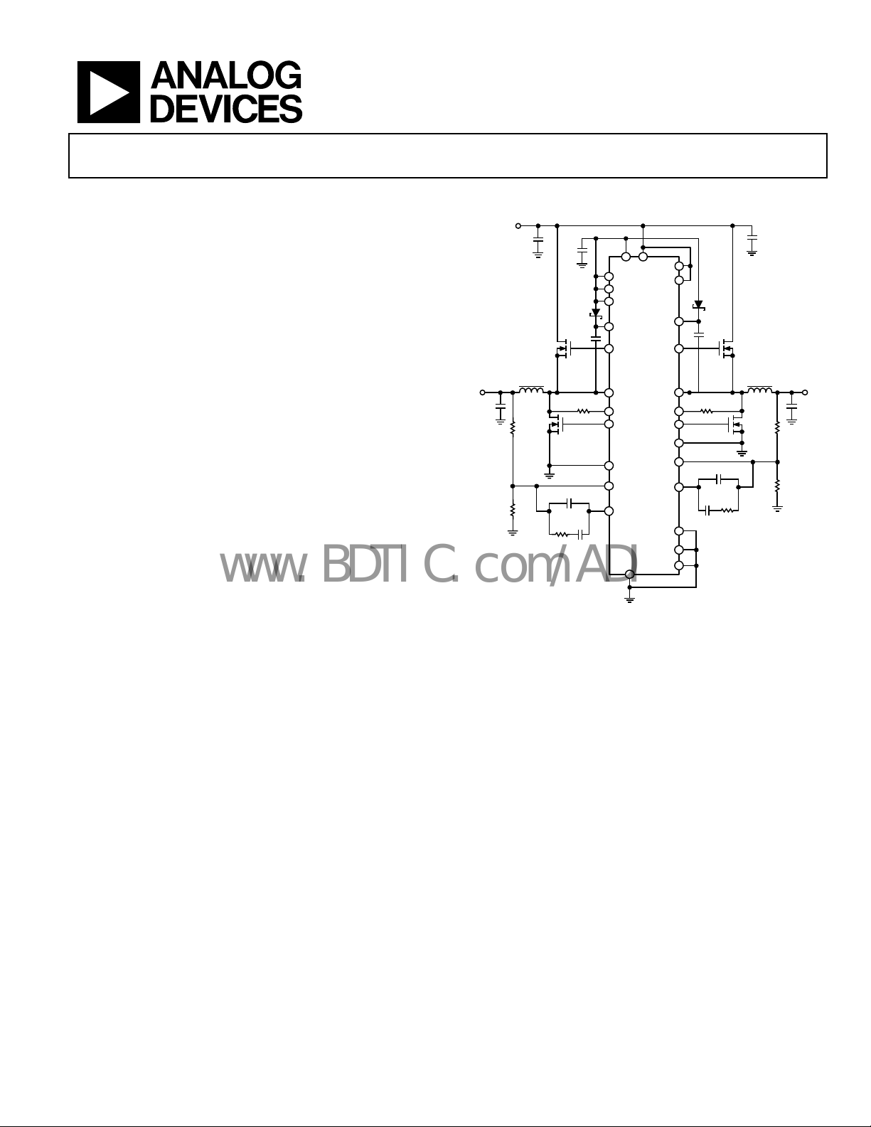
TYPICAL APPLICATION CIRCUIT
IN = 12V
390pF
4.53kΩ
180µF
IRLR7807Z
2kΩ
1kΩ
1.8V,
8A
560µF560µF
1.2V,
6A
180µF
IRLR7807Z
2kΩ
2kΩ
1µF
EN1
PV IN
TRK1
EN2
TRK2
VREG
BST2
0.47µF
2.2µH 2.2µH
IRFR3709Z
3900pF
4.53kΩ
BST1
DH2
DH1
ADP1823
SW2
SW1
2kΩ 2kΩ
390pF
CSL1
DL1
PGND1
FB1
COMP1
GND
Figure 1.
CSL2
DL2
PGND2
FB2
COMP2
FREQ
LDOSD
SYNC
0.47µF
IRFR3709Z
3900pF
05936-001
GENERAL DESCRIPTION
The ADP1823 is a versatile, dual, interleaved, synchronous,
PWM buck controller that generates two independent output
rails from an input of 3.7 V to 20 V, with a power input voltage
that ranges from 1 V to 24 V. Each controller can be configured
to provide output voltages from 0.6 V to 85% of the input voltage
and is sized to handle large MOSFETs for point-of-load regulators.
The two channels operate 180° out of phase, reducing stress on
the input capacitor and allowing smaller, low cost components.
The ADP1823 is ideal for a wide range of high power applications,
such as DSP and processor core I/O power, and general-purpose
power in telecommunications, medical imaging, PCs, gaming,
and industrial applications.
Rev. D
Information furnished by Analog Devices is believed to be accurate and reliable. However, no
responsibility is assumed by Anal og Devices for its use, nor for any infringements of patents or ot her
rights of third parties that may result from its use. Specifications subject to change without notice. No
license is granted by implication or otherwise under any patent or patent rights of Analog Devices.
Trademarks and registered trademarks are the property of their respective owners.
The ADP1823 operates at a pin-selectable, fixed switching
f
requency of either 300 kHz or 600 kHz, minimizing external
component size and cost. For noise sensitive applications, it can
also be synchronized to an external clock to achieve switching
frequencies between 300 kHz and 1 MHz. The ADP1823 includes
soft start protection to prevent inrush current from the input
supply during startup, reverse current protection during soft
start for precharged outputs, as well as a unique adjustable
lossless current-limit scheme using external MOSFET sensing.
For applications requiring power supply sequencing, the
AD
P1823 also provides tracking inputs that allow the output
voltages to track during startup, shutdown, and faults. This
feature can also be used to implement DDR memory bus
termination.
The ADP1823 is specified over the −40°C to +125°C junction
emperature range and is available in a 32-lead LFCSP.
t
One Technology Way, P.O. Box 9106, Norwood, MA 02062-9106, U.S.A.
Tel: 781.329.4700 www.analog.com
Fax: 781.461.3113 ©2006–2007 Analog Devices, Inc. All rights reserved.
Page 2

ADP1823
www.BDTIC.com/ADI
TABLE OF CONTENTS
Features .............................................................................................. 1
Applications....................................................................................... 1
Typical Applicat i o n C i rc uit ............................................................. 1
General Description......................................................................... 1
Revision History ............................................................................... 2
Specifications..................................................................................... 3
Absolute Maximum Ratings............................................................ 5
ESD Caution.................................................................................. 5
Functional Block Diagram .............................................................. 6
Pin Configuration and Function Descriptions............................. 7
Typical Performance Characteristics ............................................. 9
Theory of Operation ...................................................................... 13
Input Power ................................................................................. 13
Start-Up Logic............................................................................. 13
Internal Linear Regulator .......................................................... 13
Oscillator and Synchronization................................................ 13
Error Amplifier........................................................................... 14
Soft Start ......................................................................................14
Power OK Indicator ................................................................... 14
Tr ac ki n g ....................................................................................... 14
MOSFET Drivers........................................................................ 15
Current Limit .............................................................................. 15
Applications Information.............................................................. 16
Selecting the Input Capacitor ................................................... 16
Selecting the MOSFETs ............................................................. 17
Setting the Current Limit .......................................................... 18
Feedback Voltage Divider ......................................................... 18
Compensating the Voltage Mode Buck Regulator................. 19
Soft Start...................................................................................... 22
Volt a ge Tr ack in g ......................................................................... 22
Coincident Tracking .................................................................. 23
Ratiometric Tracking................................................................. 23
Thermal Considerations............................................................ 24
PCB Layout Guidelines.................................................................. 25
LFCSP Considerations............................................................... 26
Application Circuits ....................................................................... 27
Outline Dimensions ....................................................................... 29
Ordering Guide .......................................................................... 29
REVISION HISTORY
10/07—Rev. C to Rev D
Changes to Table 1............................................................................ 3
Changes to Equation 33 and Type III Compensator Section ... 21
7/07—Rev. B to Rev C
hanges to Figure 34...................................................................... 27
C
5/07—Rev. A to Rev. B
C
hanges to Features Section............................................................ 1
Changes to General Description Section ...................................... 1
Changes to Power Supply and Logic Thresholds Sections.......... 3
Changes to Absolute Maximum Ratings Section......................... 5
Changes to Figure 17...................................................................... 11
Changes to Theory of Operation Section.................................... 13
Changes to Current Limit Section................................................ 15
Changes to Setting the Current Limit Section............................ 18
Changes to Compensating the Voltage Mode Buck
Regulator Section............................................................................ 19
Inserted Figure 25........................................................................... 19
Deleted Table 4................................................................................ 27
Changes to Application Circuits Section..................................... 27
Changes to Figure 34...................................................................... 27
11/06—Rev. 0 to Rev. A
C
hanges to Features and Applications Sections ............................1
Changes to Specifications Section...................................................3
Changes to Absolute Maximum Ratings Section..........................5
Replaced Theory of Operation Section ....................................... 13
Added Feedback Voltage Divider Section................................... 18
Changes to Ratiometric Tracking Section................................... 23
Replaced PCB Layout Guidelines Section................................... 25
Added Application Circuits Section ............................................ 29
Changes to Ordering Guide.......................................................... 31
4/06—Revision 0: Initial Version
Rev. D | Page 2 of 32
Page 3
ADP1823
www.BDTIC.com/ADI
SPECIFICATIONS
IN = 12 V, ENx = FREQ = PV = VREG = 5 V, SYNC = GND, TJ = −40°C to +125°C, unless otherwise specified. All limits at temperature
extremes are guaranteed via correlation using standard statistical quality control (SQC). Typical values are at T
Table 1.
Parameter Conditions Min Typ Max Unit
POWER SUPPLY
IN Input Voltage PV = VREG (using internal regulator) 5.5 20 V
IN = PV = VREG (not using internal regulator) 3.7 5.5 V
IN Quiescent Current Not switching, I
IN Shutdown Current EN1 = EN2 = GND 10 20 A
VREG Undervoltage Lockout Threshold VREG rising 2.4 2.7 2.9 V
VREG Undervoltage Lockout Hysteresis 0.125 V
ERROR AMPLIFIER
FB1, FB2 Regulation Voltage TA = 25°C, TRK1, TRK2 > 700 mV 597 600 603 mV
T
T
T
FB1, FB2 Input Bias Current 100 nA
Open-Loop Voltage Gain 70 dB
Gain-Bandwidth Product 20 MHz
COMP1, COMP2 Sink Current 600 A
COMP1, COMP2 Source Current 120 A
COMP1, COMP2 Clamp High Voltage 2.4 V
COMP1, COMP2 Clamp Low Voltage 0.75 V
LINEAR REGULATOR
VREG Output Voltage TA = 25°C, I
VREG Load Regulation I
VREG Line Regulation IN = 7 V to 20 V, I
VREG Current Limit VREG = 4 V 220 mA
VREG Short-Circuit Current VREG < 0.5 V 50 140 200 mA
IN to VREG Dropout Voltage I
VREG Minimum Output Capacitance 1 F
PWM CONTROLLER
PWM Ramp Voltage Peak SYNC = GND 1.3 V
DH1, DH2 Maximum Duty Cycle FREQ = GND (300 kHz) 85 90 %
DH1, DH2 Minimum Duty Cycle FREQ = GND (300 kHz) 1 3 %
SOFT START
SS1, SS2 Pull-Up Resistance SS1, SS2 = GND 90 kΩ
SS1, SS2 Pull-Down Resistance SS1, SS2 = 0.6 V 6 kΩ
SS1, SS2 to FB1, FB2 Offset Voltage SS1, SS2 = 0 mV to 500 mV −45 mV
SS1, SS2 Pull-Up Voltage 0.8 V
TRACKING
TRK1, TRK2 Common-Mode Input Voltage Range 0 600 mV
TRK1, TRK2 to FB1, FB2 Offset Voltage TRK1, TRK2 = 0 mV to 500 mV −5 +5 mV
TRK1, TRK2 Input Bias Current 100 nA
= 0°C to 85°C, TRK1, TRK2 > 700 mV 591 609 mV
J
= −40°C to +125°C, TRK1, TRK2 > 700 mV 588 612 mV
J
= 0°C to 70°C, TRK1, TRK2 > 700 mV 595 605 mV
J
IN = 7 V to 20 V, I
= −40°C to +85°C
T
A
= 0 mA to 100 mA, IN = 12 V −40 mV
VREG
= 100 mA, IN < 5 V 0.7 1.4 V
VREG
= 0 mA 1.5 3 mA
VREG
= 20 mA 4.85 5.0 5.15 V
VREG
= 0 mA to 100 mA,
VREG
= 20 mA 1 mV
VREG
= 25°C.
A
4.75 5.0 5.25 V
Rev. D | Page 3 of 32
Page 4

ADP1823
www.BDTIC.com/ADI
Parameter Conditions Min Typ Max Unit
OSCILLATOR
Oscillator Frequency SYNC = FREQ = GND (fSW = f
SYNC = GND, FREQ = VREG (fSW = f
SYNC Synchronization Range
1
FREQ = GND, SYNC = 600 kHz to 1.2 MHz (fSW = f
FREQ = VREG, SYNC = 1.2 MHz to 2 MHz (fSW = f
SYNC Minimum Input Pulse Width 200 ns
CURRENT SENSE
CSL1, CSL2 Threshold Voltage Relative to PGND −30 0 +30 mV
CSL1, CSL2 Output Current CSL1, CSL2 = PGND 44 50 56 A
Current Sense Blanking Period 100 ns
GATE DRIVERS
DH1, DH2 Rise Time CDH = 3 nF, V
DH1, DH2 Fall Time CDH = 3 nF, V
− VSW = 5 V 15 ns
BST
− VSW = 5 V 10 ns
BST
DL1, DL2 Rise Time CDL = 3 nF 15 ns
DL1, DL2 Fall Time CDL = 3 nF 10 ns
DH to DL, DL to DH Dead Time 40 ns
LOGIC THRESHOLDS
SYNC, FREQ, LDOSD Input High Voltage 2.2 V
SYNC, FREQ, LDOSD Input Low Voltage 0.4 V
SYNC, FREQ Input Leakage Current SYNC, FREQ = 0 V to 5.5 V 1 A
LDOSD Pull-Down Resistance 100 kΩ
EN1, EN2 Input High Voltage IN = 3.7 V to 20 V 2.0 V
EN1, EN2 Input Low Voltage IN = 3.7 V to 20 V 0.8 V
EN1, EN2 Current Source EN1, EN2 = 0 V to 3.0 V −0.05 −0.6 −1.5 A
EN1, EN2 Input Impedance to 5 V Zener EN1, EN2 = 5.5 V to 20 V 100 kΩ
THERMAL SHUTDOWN
Thermal Shutdown Threshold
Thermal Shutdown Hysteresis
2
2
145
15
POWER GOOD
FB1, UV2 Overvoltage Threshold V
, V
rising 750 mV
FB1
UV2
FB1, UV2 Overvoltage Hysteresis 50 mV
FB1, UV2 Undervoltage Threshold V
, V
rising 550 mV
FB1
UV2
FB1, UV2 Undervoltage Hysteresis 50 mV
POK1, POK2 Propagation Delay 8 s
POK1, POK2 Off Leakage Current V
POK1, POK2 Output Low Voltage I
POK1
POK1
, V
= 5.5 V 1 A
POK2
, I
= 10 mA 150 500 mV
POK2
UV2 Input Bias Current 10 100 nA
1
SYNC input frequency is 2× the single-channel switching frequency. The SYNC frequency is divided by 2, and the separate phases were used to clock the controllers.
2
Guaranteed by design and not subject to production test.
) 240 300 370 kHz
OSC
) 480 600 720 kHz
OSC
/2) 300 600 kHz
SYNC
/2) 600 1000 kHz
SYNC
°C
°C
Rev. D | Page 4 of 32
Page 5
ADP1823
www.BDTIC.com/ADI
ABSOLUTE MAXIMUM RATINGS
Table 2.
Parameter Rating
IN, EN1, EN2 −0.3 V to +20 V
BST1, BST2 −0.3 V to +30 V
BST1, BST2 to SW1, SW2 −0.3 V to +6 V
CSL1, CSL2 −1 V to +30 V
SW1, SW2 −2 V to +30 V
DH1 SW1 − 0.3 V to BST1 + 0.3 V
DH2 SW2 − 0.3 V to BST2 + 0.3 V
DL1, DL2 to PGND −0.3 V to PV + 0.3 V
PGND to GND ±2 V
LDOSD, SYNC, FREQ, COMP1,
−0.3 V to +6 V
COMP2, SS1, SS2, FB1, FB2, VREG,
PV, POK1, POK2, TRK1, TRK2
θJA 4-Layer
(JEDEC Standard Board)
1, 2
45°C/W
Operating Ambient Temperature −40°C < TA < +85°C
Operating Junction Temperature
3
−55°C < TJ < +125°C
Storage Temperature Range −65°C to +150°C
1
Measured with exposed pad attached to PCB.
2
Junction-to-ambient thermal resistance (θJA) of the package is based on
modeling and calculation using a 4-layer board. The junction-to-ambient
thermal resistance is application and board-layout dependent. In appl ications
where high maximum power dissipation exists, attention to thermal
dissipation issues in board design is required. For more information, refer
to Application Note AN-772, A Design and Manufacturing Guide for the Lead
Frame Chip Scale Package (LFCSP).
3
In applications where high power dissipation and poor package thermal
resistance are present, the maximum ambient temperature may have to be
derated. Maximum ambient temperature (T
maximum operating junction temperature (T
power dissipation of the device in the application (P
to-ambient thermal resistance of the part/package in the application (θJA),
and is given by: T
A_MAX
= T
J_MAX_OP
− (θJA × P
) is dependent on the
A_MAX
= 125oC), the maximum
J_MAX_OP
D_MAX
).
D_MAX
), and the junction-
Stresses above those listed under Absolute Maximum Ratings
may cause permanent damage to the device. This is a stress
rating only; functional operation of the device at these or any
other conditions above those indicated in the operational
section of this specification is not implied. Exposure to absolute
maximum rating conditions for extended periods may affect
device reliability.
ESD CAUTION
Rev. D | Page 5 of 32
Page 6
ADP1823
www.BDTIC.com/ADI
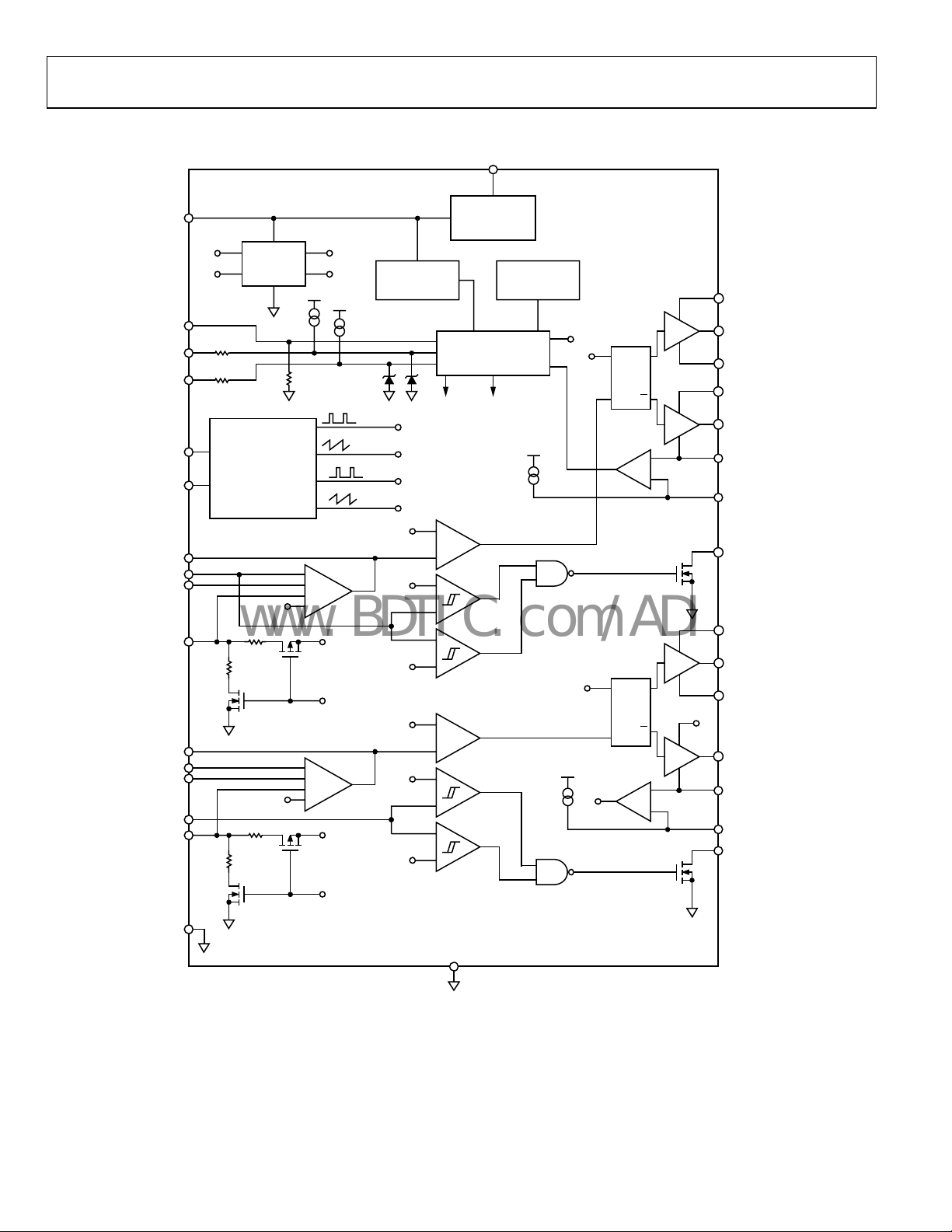
FUNCTIONAL BLOCK DIAGRAM
VREG
0.75V
0.55V
VREG
–
+
+
+
0.8V
FAULT1
–
+
+
+
0.8V
FAULT2
VREG
LDOSD
EN1
EN2
FREQ
SYNC
COMP1
FB1
TRK1
SS1
COMP2
FB2
TRK2
UV2
SS2
0.6V
0.8V
OSCILLATOR
PHASE 1 = 0°
PHASE 2 = 180°
REF
0.6V
0.6V
CK1
RAMP1
CK2
RAMP2
RAMP1
RAMP2
0.75V
0.55V
0.75V
0.55V
UVLO
+
–
+
–
+
–
+
–
+
–
+
–
IN
LINEAR REG
LOGIC
FAULT2FAULT1
50µA
THERMAL
SHUTDOWN
VREG
50µA
ILIM2
CK2
VREG
ILIM1
CK1
ILIM2
PWM
R
PWM
R
ADP1823
QS
Q
+
–
QS
Q
+
–
BST1
DH1
SW1
PV
DL1
PGND1
CSL1
POK1
BST2
DH2
SW2
PV
DL2
PGND2
CSL2
POK2
GND
BOTTOM PADDLE
OF LFCSP
Figure 2.
Rev. D | Page 6 of 32
05936-002
Page 7
ADP1823
www.BDTIC.com/ADI
PIN CONFIGURATION AND FUNCTION DESCRIPTIONS
OMP1
S1
C
TRK1
S
VREG
IN
LDOSD
EN2
EN1
28
27
26
25
29
31
30
32
1FB1
2SYNC
3FREQ
4GND
5UV2
6FB2
7COMP2
8TRK2
PIN 1
INDICATOR
ADP1823
TOP VIEW
(Not to Scale)
1
9
1
10
12
SS2
DH2
BST2
POK2
13
SW2
24 PO K1
23 BST 1
22 DH1
21 SW 1
20 CSL 1
19 PG ND1
18 DL1
17 PV
14
15
16
DL2
CSL2
PGND2
05936-003
Figure 3. Pin Configuration
Table 3. Pin Function Descriptions
Pin No. Mnemonic Description
1 FB1
Feedback Voltage Input for Channel 1. Connect a resistor divider fr
om the buck regulator output to GND and
tie the tap to FB1 to set the output voltage.
2 SYNC
Frequency Synchronization Input. Accepts external signal between 600 kHz and 1.2 MHz or between 1.2 MHz
and 2 MH
z depending on whether FREQ is low or high, respectively. Connect SYNC to ground if not used.
3 FREQ Frequency Select Input. Low for 300 kHz or high for 600 kHz.
4 GND
5 UV2
Ground. Connect to a ground plane directly beneath the ADP1823. Tie the bottom of the feedback dividers to
this GND
Input to the POK2 Undervoltage and Overvoltage Compar
.
ators. For the default thresholds, connect UV2
directly to FB2. For some tracking applications, connect UV2 to an extra tap on the FB2 voltage divider string.
6 FB2
Feedback Voltage Input for Channel 2. Connect a resistor divider fr
om the buck regulator output to GND and
tie the tap to FB2 to set the output voltage.
7 COMP2 Error Amplifier Output for Channel 2. Connect an RC network from COMP2 to FB2 to compensate Channel 2.
8 TRK2
Tracking Input for Channel 2. To track a master voltage
, drive TRK2 from a voltage divider to the master
voltage. If the tracking function is not used, connect TRK2 to VREG.
9 SS2 Soft Start Control Input. Connect a capacitor from SS2 to GND to set the soft start period.
10 POK2
Open-Drain Power OK Output for Channel 2. Sinks current when UV2 is out of r
egulation. Connect a pull-up
resistor from POK2 to VREG.
11 BST2
Boost Capacitor Input for Channel 2. Powers the high-side ga
te driver, DH2. Connect a 0.22 F to 0.47 F
ceramic capacitor from BST2 to SW2 and a Schottky diode from PV to BST2.
12 DH2 High-Side (Switch) Gate Driver Output for Channel 2.
13 SW2 Switch Node Connection for Channel 2.
14 CSL2
Current Sense Comparator Inverting Input for Channel 2. Connect a resistor between CSL2 and SW2 to set
rent-limit offset.
the cur
15 PGND2 Ground for Channel 2 Gate Driver. Connect to a ground plane directly beneath the ADP1823.
16 DL2 Low-Side (Synchronous Rectifier) Gate Driver Output for Channel 2.
17 PV
Positive Input Voltage for Gate Driver DL1 and Gate Driv
er DL2. Connect PV to VREG and bypass to ground
with a 1 µF capacitor.
18 DL1 Low-Side (Synchronous Rectifier) Gate Driver Output for Channel 1.
19 PGND1 Ground for Channel 1 Gate Driver. Connect to a ground plane directly beneath the ADP1823.
20 CSL1
Current Sense Comparator Inverting Input for Channel 1. Connect a resistor between CSL1 and SW1 to set
rent-limit offset.
the cur
21 SW1 Switch Node Connection for Channel 1.
22 DH1 High-Side (Switch) Gate Driver Output for Channel 1.
23 BST1
Boost Capacitor Input for Channel 1. Powers the high-side ga
te driver, DH1. Connect a 0.22 F to 0.47 F
ceramic capacitor from BST1 to SW1 and a Schottky diode from PV to BST1.
Rev. D | Page 7 of 32
Page 8
ADP1823
www.BDTIC.com/ADI
Pin No. Mnemonic Description
24 POK1
25 EN1
26 EN2
27 LDOSD
28 IN
29 VREG
30 SS1 Soft Start Control Input. Connect a capacitor from SS1 to GND to set the soft start period.
31 TRK1
32 COMP1 Error Amplifier Output for Channel 1. Connect an RC network from COMP1 to FB1 to compensate Channel 1.
Open-Drain Power OK Output for Channel 1. Sinks current when FB1 is out of r
resistor from POK1 to VREG.
Enable Input for Channel 1. Drive EN1 high to turn on the Chann
the Channel 1 controller. Enabling starts the internal LDO. Tie to IN for automatic startup.
Enable Input for Channel 2. Drive EN2 high to turn on the Chann
the Channel 2 controller. Enabling starts the internal LDO. Tie to IN for automatic startup.
LDO Shut-Down Input. Only used to shut do
Otherwise, connect LDOSD to GND or leave it open because it has an internal 100 kΩ pull-down resistor.
Input Supply to the Internal Linear Regulator. Drive IN with 5.5
For input voltages between 3.7 V and 5.5 V, tie IN to VREG and PV.
Output of the Internal Linear Regulator (LDO). The internal cir
Bypass VREG to the ground plane with a 1 F ceramic capacitor.
Tracking Input for Channel 1. To track a master voltage, dr
If the tracking function is not used, connect TRK1 to VREG.
wn the LDO in those applications where IN is tied directly to VREG.
el 1 controller, and drive it low to turn off
el 2 controller, and drive it low to turn off
V to 20 V to power the ADP1823 from the LDO.
cuitry and gate drivers are powered from VREG.
ive TRK1 from a voltage divider to the master voltage.
egulation. Connect a pull-up
Rev. D | Page 8 of 32
Page 9
ADP1823
www.BDTIC.com/ADI
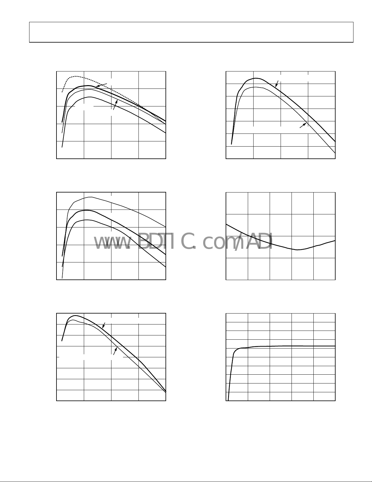
TYPICAL PERFORMANCE CHARACTERISTICS
95
90
85
80
EFFICIENCY (%)
75
VIN = 5V
VIN = 12V
VIN = 20V
VIN = 15V
92
90
88
86
84
EFFICIENCY (%)
82
80
SWITCHI NG FREQUENCY = 300kHz
SWITCHI NG FREQUENCY = 600kHz
70
02
Figure 4. Efficiency vs. Load Current, V
51015
LOAD CURRENT (A)
= 1.8 V, 300 kHz Switching
OUT
0
05936-004
78
020
Figure 7. Efficiency vs. Load Current, V
95
V
= 3.3V
OUT
90
85
80
EFFICIENCY (%)
75
70
02
51015
Figure 5. Efficiency vs. Load Current, V
94
92
90
88
86
SWITCHING FREQUENCY = 600kHz
84
EFFICIENCY (%)
82
80
78
02
51015
Figure 6. Efficiency vs. Load Current, V
V
= 1.8V
OUT
V
= 1.2V
OUT
LOAD CURRENT (A)
= 12 V, 300 kHz Switching
IN
SWITCHI NG FREQUENCY = 300kHz
LOAD CURRENT (A)
= 5 V, V
IN
OUT
= 1.8 V
0
05936-005
0
05936-006
4.980
4.975
4.970
VREG VOLTAGE (V)
4.965
4.960
–40 85
Figure 8. VREG Voltage vs. Temperature
4.970
4.968
4.966
4.964
4.962
4.960
VREG (V)
4.958
4.956
4.954
4.952
4.950
520
Figure 9. VREG vs. Input Voltage, 10 mA Load
51015
LOAD CURRENT (A)
= 12 V, V
IN
OUT
–15 10 35 60
TEMPERATURE ( °C)
811
INPUT VOLTAGE (V)
1417
= 1.8 V
05936-007
05936-008
05936-009
Rev. D | Page 9 of 32
Page 10
ADP1823
www.BDTIC.com/ADI
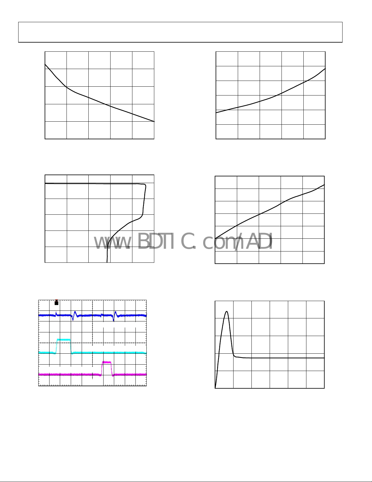
4.960
0.6010
4.956
4.952
VREG (V)
4.948
4.944
4.940
0 100
20 40 60 80
LOAD CURRENT (mA)
Figure 10. VREG vs. Load Current, VIN = 12 V
5
4
3
2
VREG OUTPUT (V)
1
0.6005
0.6000
0.5995
0.5990
FEEDBACK VOLT AGE (V)
0.5985
0.5980
–40 85
05936-010
–15 10 35 60
TEMPERATURE ( °C)
05936-013
Figure 13. Feedback Voltage vs. Temperature, VIN = 12 V
330
320
310
300
290
FREQUENCY (Hz)
280
270
0
0 50 100 150 200 250
LOAD CURRENT (mA)
Figure 11. VREG Current-Limit Foldback
T
VREG, AC-CO UPLED, 1V/ DIV
SW2 PIN, V
= 1.2V, 10V /DIV
OUT
SW1 PIN, V
200ns/DIV
= 1.8V, 10V/DIV
OUT
Figure 12. VREG Output During Normal Operation
260
–40 85
05936-011
–15 10 35 60
TEMPERATURE ( °C)
05936-014
Figure 14. Switching Frequency vs. Temperature, VIN = 12 V
5
4
3
2
SUPPLY CURRENT (mA)
1
05936-012
0
22
5 8 11 14 17
SUPPLY VOLTAGE (V)
0
05936-015
Figure 15. Supply Current vs. Supply Voltage
Rev. D | Page 10 of 32
Page 11

ADP1823
www.BDTIC.com/ADI
T
V
, AC-COUPLE D,
OUT1
100mV/DIV
LOAD ON
LOAD OFF LOAD OFF
T
EXTERNAL CL OCK, F REQUENCY = 1MHz
SW PIN, CHANNEL 1
SW PIN, CHANNEL 2
100µs/DIV
Figure 16. 1.5 A to 15 A Load Transient Response, VIN = 12 V
T
SHORT CIRCUIT APPLIED
SS1, 0.5V/ DIV
V
, 0.5V/DIV
OUT1
INPUT CURRENT, 0.2A/DIV
4ms/DIV
SHORT CIRCUIT REMOVED
Figure 17. Output Short-Circuit Response
T
5936-016
400ns/DIV
05936-019
Figure 19. Out-of-Phase Switching, External 1 MHz Clock
T
EXTERNAL CLOCK, FREQ UENCY = 2MHz
SW PIN, CHANNEL 1
SW PIN, CHANNEL 2
05936-017
200ns/DIV
05936-020
Figure 20. Out-of-Phase Switching, External 2 MHz Clock
VIN = 12V
T
V
, 2V/DIV
OUT1
SWIT CH NODE
CHANNEL 1
SWITCH NODE CHANNEL 2
400ns/DIV
05936-018
Figure 18. Out-of-Phase Switching, Internal Oscillator
Rev. D | Page 11 of 32
10ms/DIV
Figure 21. Enable Pin Response, V
EN1, 5V/DIV
= 12 V
IN
05936-021
Page 12

ADP1823
www.BDTIC.com/ADI
T
SOFT START, 1V/DIV
4ms/DIV
Figure 22. Power-On Response, EN Tied to V
TRACK PIN VOL TAGE,
200mV/DIV
FEEDBACK PIN
VOLTAG E, 200mV/DIV
T
VIN, 5V/DIV
V
, 2V/DIV
OUT
EN2 PIN, 5V/DIV
V
, 2V/DIV
OUT2
V
, 2V/DIV
OUT1
05936-022
IN
EN1 = 5V
Figure 24. Coincident Voltage Tracking Response
40ms/DIV
05936-024
20ms/DIV
05936-023
Figure 23. Output Voltage Tracking Response
Rev. D | Page 12 of 32
Page 13

ADP1823
www.BDTIC.com/ADI
THEORY OF OPERATION
The ADP1823 is a dual, synchronous, PWM buck controller
capable of generating output voltages down to 0.6 V and output
currents in the tens of amps. The switching of the regulators is
interleaved for reduced current ripple. It is ideal for a wide
range of applications, such as DSP and processor core I/O
supplies, general-purpose power in telecommunications,
medical imaging, gaming, PCs, set-top boxes, and industrial
controls. The ADP1823 controller operates directly from 3.7 V
to 20 V, and the power stage input voltage range is 1 V to 24 V,
which applies directly to the drain of the high-side external
power MOSFET. It includes fully integrated MOSFET gate
drivers and a linear regulator for internal and gate drive bias.
The ADP1823 operates at a fixed 300 kHz or 600 kHz switching
requency. The ADP1823 can also be synchronized to an external
f
clock to switch at up to 1 MHz per channel. The ADP1823
includes soft start to prevent inrush current during startup, as
well as a unique adjustable lossless current limit.
The ADP1823 offers flexible tracking for startup and shutdown
equencing. It is specified over the −40°C to +125°C temperature
s
range and is available in a space-saving, 5 mm × 5 mm,
32-lead LFCSP.
INPUT POWER
The ADP1823 is powered from the IN pin up to 20 V. The
internal low dropout linear regulator, VREG, regulates the IN
voltage down to 5 V. The control circuits, gate drivers, and
external boost capacitors operate from the LDO output. Tie
the PV pin to VREG and bypass VREG with a 1 μF or greater
capacitor.
The ADP1823 phase shifts the switching of the two step-down
co
nverters by 180°, thereby reducing the input ripple current.
The phase shift reduces the size and cost of the input capacitors.
The input voltage should be bypassed with a capacitor close to
the high-side switch MOSFETs (see the
Ca
pacitor section). In addition, a minimum 0.1 µF ceramic
ca
pacitor should be placed as close as possible to the IN pin.
The VREG output is sensed by the undervoltage lockout
(UVL
O) circuit to be certain that enough voltage headroom
is available to run the controllers and gate drivers. As VREG
rises above about 2.7 V, the controllers are enabled. The IN
voltage is not directly monitored by UVLO. If the IN voltage is
insufficient to allow VREG to be above the UVLO threshold,
the controllers are disabled but the LDO continues to operate.
The LDO is enabled whenever either EN1 or EN2 is high, even
if VREG is below the UVLO threshold.
If the desired input voltage is between 3.7 V and 5.5 V, connect
IN d
irectly to the VREG pin and the PV pin, and drive LDOSD
high to disable the internal regulator. The ADP1823 requires
that the voltage at VREG and PV be limited to no more than 5.5
V, which is the only application where the LDOSD pin is used.
Selecting the Input
Otherwise, it should be grounded or left open. LDOSD has an
internal 100 k pull-down resistor.
Although IN is limited to 20 V, the switching stage can run from
up
to 24 V, and the BST pins can go to 30 V to support the gate
drive. Dissipation on the ADP1823 can be limited by running IN
from a low voltage rail while operating the switches from the high
voltage rail.
START-UP LOGIC
The ADP1823 features independent enable inputs for each
channel. Drive EN1 or EN2 high to enable their respective
controllers. The LDO starts when either channel is enabled.
When both controllers are disabled, the LDO is disabled and
the IN quiescent current drops to about 10 μA. For automatic
startup, connect EN1 and/or EN2 to IN. The enable pins are
20 V compliant, but they sink current through an internal
100 k resistor when the EN pin voltage exceeds about 5 V.
INTERNAL LINEAR REGULATOR
The internal linear regulator, VREG, is low dropout, which means
it can regulate its output voltage close to the input voltage.
VREG powers up the internal control and provides bias for
the gate drivers. It is guaranteed to have more than 100 mA of
output current capability, which is sufficient to handle the gate
drive requirements of typical logic threshold MOSFETs driven
at up to 1 MHz. VREG should always be bypassed with a 1 μF
or greater capacitor.
Because the LDO supplies the gate drive current, the output of
VREG i
s subject to sharp transient currents as the drivers switch
and the boost capacitors recharge during each switching cycle.
The LDO has been optimized to handle these transients without
overload faults. Due to the gate drive loading, using the VREG
output for other auxiliary system loads is not recommended.
The LDO includes a current limit well above the expected
max
imum gate drive load. This current limit also includes a
short-circuit foldback to further limit the VREG current in the
event of a fault.
OSCILLATOR AND SYNCHRONIZATION
The ADP1823 internal oscillator can be set to either 300 kHz or
600 kHz. Drive the FREQ pin low for 300 kHz; drive it high for
600 kHz. The oscillator generates a start clock for each switching
phase and generates the internal ramp voltages for the PWM
modulation.
The SYNC input is used to synchronize the converter switching
requency to an external signal. The SYNC input should be
f
driven with twice the desired switching frequency, as the SYNC
input is divided by 2, and the resulting phases are used to clock
the two channels alternately.
Rev. D | Page 13 of 32
Page 14

ADP1823
www.BDTIC.com/ADI
If FREQ is driven low, the recommended SYNC input frequency
is between 600 kHz and 1.2 MHz. If FREQ is driven high, the
recommended SYNC frequency is between 1.2 MHz and
2 MHz. The FREQ setting should be carefully observed for
these SYNC frequency ranges, because the PWM voltage ramp
scales down from about 1.3 V based on the percentage of
frequency overdrive. Driving SYNC faster than recommended
for the FREQ setting results in a small ramp signal, which could
affect the signal-to-noise ratio and the modulator gain and
stability.
When an external clock is detected at the first SYNC edge, the
in
ternal oscillator is reset and clock control shifts to SYNC.
The SYNC edges then trigger subsequent clocking of the PWM
outputs. The DH rising edges appear about 400 ns after the
corresponding SYNC edge, and the frequency is locked to the
external signal. Depending on the start-up conditions of Channel 1
and Channel 2, either Channel 1 or Channel 2 can be the first
channel synchronized to the rising edge of the SYNC clock. If
the external SYNC signal disappears during operation, the
ADP1823 reverts to its internal oscillator and experiences a
delay of no more than a single cycle of the internal oscillator.
ERROR AMPLIFIER
The ADP1823 error amplifiers are operational amplifiers. The
ADP1823 senses the output voltages through external resistor
dividers at the FB1 and FB2 pins. The FB pins are the inverting
inputs to the error amplifiers. The error amplifiers compare
these feedback voltages to the internal 0.6 V reference, and
the outputs of the error amplifiers appear at the COMP1 and
COMP2 pins. The COMP pin voltages then directly control
the duty cycle of each respective switching converter.
A series/parallel RC network is tied between the FB pins and
eir respective COMP pins to provide the compensation for
th
the buck converter control loops. A detailed design procedure
for compensating the system is provided in the
he Voltage Mode Buck Regulator section.
t
The error amplifier outputs are clamped between a lower limit
of
about 0.7 V and a higher limit of about 2.4 V. When the
COMP pins are low, the switching duty cycle goes to 0%, and
when the COMP pins are high, the switching duty cycle goes
to the maximum.
The SS and TRK pins are auxiliary positive inputs to the error
am
plifiers. Whichever has the lowest voltage, SS, TRK, or the
internal 0.6 V reference controls the FB pin voltage and thus
the output. Therefore, if two or more of these inputs are close
to each other, a small offset is imposed on the error amplifier.
For example, if TRK approaches the 0.6 V reference, the FB
sees about 18 mV of negative offset at room temperature. For
this reason, the soft start pins have a built-in negative offset
and they charge to 0.8 V. If the TRK pins are not used, they
should be tied high to VREG.
Compensating
SOFT START
The ADP1823 employs a programmable soft start that reduces
input current transients and prevents output overshoot. The SS1
and SS2 pins drive auxiliary positive inputs to their respective
error amplifiers, thus the voltage at these pins regulates the voltage
at their respective feedback control pins.
Program soft start by connecting capacitors from SS1 and SS2
GND. When starting up, the capacitor charges from an
to
internal 90 kΩ resistor to 0.8 V. The regulator output voltage
rises with the voltage at its respective soft start pin, allowing the
output voltage to rise slowly, reducing inrush current. See the
Soft Start section in the Applications Information section for
information.
more
When a controller is disabled or experiences a current fault, the
so
ft start capacitor discharges through an internal 6 k resistor,
so that at restart or recovery from fault, the output voltage soft
starts again.
POWER OK INDICATOR
The ADP1823 features open-drain, power OK outputs, POK1
and POK2, which sink current when their respective output
voltages drop, typically 8% below the nominal regulation
voltage. The POK pins also go low for overvoltage of typically
25%. Use this output as a logical power-good signal by connecting pull-up resistors from POK1 and POK2 to VREG.
The POK1 comparator directly monitors FB1, and the threshold
fixed at 550 mV for undervoltage and 750 mV for overvoltage.
is
However, the POK2 undervoltage and overvoltage comparator
input is connected to UV2 rather than FB2. For the default
thresholds at FB2, connect UV2 directly to FB2.
In a ratiometric tracking configuration, however, Channel 2 can
e configured to be a fraction of a master voltage, and thus FB2
b
is regulated to a voltage lower than the 0.6 V internal reference.
In this configuration, UV2 can be tied to a different tap on the
feedback divider, allowing a POK2 indication at an appropriate
output voltage threshold. See the
U
ndervoltage Threshold for Ratiometric Tracking section.
Setting the Channel 2
TRACKING
The ADP1823 features tracking inputs, TRK1 and TRK2, which
make the output voltages track another master voltage. Voltage
tracking is especially useful in core and I/O voltage sequencing
applications where one output of the ADP1823 can be set to
track and not exceed the other, or in other multiple output
systems where specific sequencing is required.
The internal error amplifiers include three positive inputs, the
ternal 0.6 V reference voltage and their respective SS and TRK
in
pins. The error amplifiers regulate the FB pins to the lowest of
the three inputs. To track a supply voltage, tie the TRK pin to a
resistor divider from the voltage to be tracked. See the
Tr
a ck in g section.
Vo lt a ge
Rev. D | Page 14 of 32
Page 15

ADP1823
www.BDTIC.com/ADI
MOSFET DRIVERS
The DH1 and DH2 pins drive the high-side switch MOSFETs.
These boosted 5 V gate drivers are powered by bootstrap capacitor
circuits. This configuration allows the high-side, N-channel
MOSFET gate to be driven above the input voltage, allowing
full enhancement and a low voltage drop across the MOSFET.
The bootstrap capacitors are connected from the SW pins to
their respective BST pins. The bootstrap Schottky diodes from
the PV pin to the BST pins recharge the bootstrap capacitors every
time the SW nodes go low. Use a bootstrap capacitor value
greater than 100× the high-side MOSFET input capacitance.
In practice, the switch node can run up to 24 V of input voltage,
he boost nodes can operate more than 5 V above this to
and t
allow full gate drive. The IN pin can be run from 3.7 V to 20 V,
which can provide an advantage, for example, in the case of high
frequency operation from very high input voltage. Dissipation on
the ADP1823 can be limited by running IN from a lower voltage
rail while operating the switches from the high voltage rail.
The switching cycle is initiated by the internal clock signal. The
h-side MOSFET is turned on by the DH driver, and the SW
hig
node goes high, pulling up on the inductor. When the internally
generated ramp signal crosses the COMP pin voltage, the switch
MOSFET is turned off and the low-side synchronous rectifier
MOSFET is turned on by the DL driver. Active break-beforemake circuitry, as well as a supplemental fixed dead time, are
used to prevent cross-conduction in the switches.
The DL1 and DL2 pins provide gate drive for the low-side
M
OSFET synchronous rectifiers. Internal circuitry monitors
the external MOSFETs to ensure break-before-make switching
to prevent cross-conduction. An active dead time reduction
circuit reduces the break-before-make time of the switching to
limit the losses due to current flowing through the synchronous
rectifier body diode.
The PV pin provides power to the low-side drivers. It is limited
o 5.5 V maximum input and should have a local decoupling
t
capacitor.
The synchronous rectifiers are turned on for a minimum time
f about 200 ns on every switching cycle to sense the current.
o
This minimum on time and the nonoverlap dead times put a limit
on the maximum high-side switch duty cycle based on the selected
switching frequency. Typically, this is about 90% at 300 kHz
switching, and at 1 MHz switching, it reduces to about 70%
maximum duty cycle.
Because the two channels are 180° out of phase, if one is operating
round 50% duty cycle, it is common for it to jitter when the
a
other channel starts switching. The magnitude of the jitter depends
somewhat on layout, but it is difficult to avoid in practice.
When the ADP1823 is disabled, the drivers shut off the external
M
OSFETs, so that the SW node becomes three-stated or
changes to high impedance.
CURRENT LIMIT
The ADP1823 employs a unique, programmable, cycle-by-cycle
lossless current-limit circuit that uses a small, ordinary, inexpensive
resistor to set the threshold. Every switching cycle, the synchronous rectifier turns on for a minimum time and the voltage
drop across the MOSFET R
cycle to determine whether the current is too high.
This measurement is done by an internal current-limit
co
mparator and an external current-limit set resistor. The
resistor is connected between the switch node (that is, the
drain of the rectifier MOSFET) and the CSL pin. The CSL pin,
which is the inverting input of the comparator, forces 50 A
through the resistor to create an offset voltage drop across it.
When the inductor current is flowing in the MOSFET rectifier,
i
ts drain is forced below PGND by the voltage drop across its
R
. If the R
DSON
external resistor, the inverting comparator input is similarly
forced below PGND and an overcurrent fault is flagged.
The normal transient ringing on the switch node is ignored for
s after the synchronous rectifier turns on; therefore, the
100 n
overcurrent condition must also persist for 100 ns in order for a
fault to be flagged.
When an overcurrent event occurs, the overcurrent comparator
p
revents switching cycles until the rectifier current has decayed
below the threshold. The overcurrent comparator is blanked
for the first 100 ns of the synchronous rectifier cycle to prevent
switch node ringing from falsely tripping the current limit. The
ADP1823 senses the current limit during the off cycle. When
the current-limit condition occurs, the ADP1823 resets the
internal clock until the overcurrent condition disappears. The
ADP1823 suppresses the start clock cycles until the overload
condition is removed. At the same time, the SS capacitor is
discharged through a 6 k resistor. The SS input is an auxiliary
positive input of the error amplifier, so it behaves like another
voltage reference. The lowest reference voltage wins.
Discharging the SS voltage causes the converter to use a lower
v
oltage reference when switching is allowed again. Therefore,
as switching cycles continue around the current limit, the output
looks roughly like a constant current source due to the rectifier
limit, and the output voltage droops as the load resistance
decreases. In the event of a short circuit, the short-circuit
output current is the current limit set by the R
is monitored cycle by cycle. When the overcurrent condition is
removed, operation resumes in soft start mode.
In the event of a short circuit, the ADP1823 also offers a
echnique for implementing a current-limit foldback with the
t
use of an additional resistor. See the
ection for more information.
s
voltage drop exceeds the preset drop on the
DSON
is measured during the off
DSON
resistor and
CL
Setting the Current Limit
Rev. D | Page 15 of 32
Page 16

ADP1823
Δ≅Δ
www.BDTIC.com/ADI
APPLICATIONS INFORMATION
SELECTING THE INPUT CAPACITOR
The input current to a buck converter is a pulse waveform. It is
zero when the high-side switch is off and approximately equal
to the load current when it is on. The input capacitor carries the
input ripple current, allowing the input power source to supply
only the dc current. The input capacitor needs sufficient ripple
current rating to handle the input ripple and ESR that is low
enough to mitigate input voltage ripple. For the usual current
ranges for these converters, good practice is to use two parallel
capacitors placed close to the drains of the high-side switch
MOSFETs, one bulk capacitor of sufficiently high current rating
as calculated in Equation 1, along with a 10 F ceramic capacitor.
Select an input bulk capacitor based on its ripple current rating.
I
f both Channel 1 and Channel 2 maximum output load currents
are about the same, the input ripple current is less than half of
the higher of the output load currents. In this case, use an input
capacitor with a ripple current rating greater than half of the
highest load current.
I
I >
RIPPLE
If the Output 1 and Output 2 load currents are significantly
different (if the smaller is less than 50% of the larger), the
procedure in Equation 1 yields a larger input capacitor than
required. In this case, the input capacitor can be chosen as in
the case of a single phase converter with only the higher load
current; therefore, first determine the duty cycle of the output
with the larger load current.
D =
In this case, the input capacitor ripple current is approximately
where:
I
is the maximum inductor or load current for the channel.
L
D is the duty cycle.
Use this method to determine the input capacitor ripple current
ting for duty cycles between 20% and 80%.
ra
For duty cycles less than 20% or greater than 80%, use an input
pacitor with a ripple current rating of I
ca
Selecting the Output LC Filter
The output LC filter attenuates the switching voltage, making
the output an almost dc voltage. The output LC filter characteristics determine the residual output ripple voltage.
Choose an inductor value such that the inductor ripple current
pproximately 1/3 of the maximum dc output load current.
is a
Using a larger value inductor results in a physical size larger
than is required, and using a smaller value results in increased
losses in the inductor and MOSFETs.
L
(1)
2
V
OUT
(2)
V
IN
)1( DDII
−≈ (3)
LRIPPLE
> 0.4 IL.
RIPPLE
Choose the inductor value by
VV
−
IN
L
=
OUT
fI
L
SW
⎞
⎛
V
OUT
⎟
⎜
⎜
⎝
(4)
⎟
V
IN
⎠
where:
L is the ind
f
is the switching frequency.
SW
V
OUT
V
IN
ΔI
is the inductor ripple current, typically 1/3 of the maximum
L
uctor value.
is the output voltage.
is the input voltage.
dc load current.
Choose the output bulk capacitor to set the desired output voltage
ipple. The impedance of the output capacitor at the switching
r
frequency multiplied by the ripple current gives the output
voltage ripple. The impedance is made up of the capacitive
impedance plus the nonideal parasitic characteristics, the
equivalent series resistance (ESR), and the equivalent series
inductance (ESL). The output voltage ripple can be
approximated with
OUT
⎛
⎜
ESRIV
L
⎜
⎝
1
8
Cf
SW
OUT
4
++Δ=Δ ESLf
SW
⎞
⎟
(5)
⎟
⎠
where:
is the output ripple voltage.
ΔV
OUT
ΔI
is the inductor ripple current.
L
ESR is the equivalent series resistance of the output capacitor
(or the parallel combination of ESR of all output capacitors).
ESL is the equivalent series inductance of the output capacitor
(or the parallel combination of ESL of all capacitors).
Note that the factors of 8 and 4 in Equation 5 would normally
e 2π for sinusoidal waveforms, but the ripple current waveform in
b
this application is triangular. Parallel combinations of different
types of capacitors, for example, a large aluminum electrolytic
in parallel with MLCCs, may give different results.
Usually, the impedance is dominated by ESR at the switching
f
requency, as stated in the maximum ESR rating on the
capacitor data sheet, so this equation reduces to
ESRIV
(6)
OUT
L
Electrolytic capacitors have significant ESL also, on the order of
5 nH to 20 nH, depending on type, size, and geometry, and PCB
traces contribute some ESR and ESL as well. However, using the
maximum ESR rating from the capacitor data sheet usually
provides some margin such that measuring the ESL is not
usually required.
Rev. D | Page 16 of 32
Page 17

ADP1823
(
)
+
www.BDTIC.com/ADI
In the case of output capacitors where the impedance of the
ESR and ESL are small at the switching frequency, for instance,
where the output capacitor is a bank of parallel MLCC
capacitors, the capacitive impedance dominates and the ripple
equation reduces to
I
L
V
≅
OUT
8
OUT
(7)
fC
SW
Make sure that the ripple current rating of the output capacitors
is gr
eater than the maximum inductor ripple current.
During a load step transient on the output, the output capacitor
s
upplies the load until the control loop has a chance to ramp the
inductor current. This initial output voltage deviation due to a
change in load is dependent on the output capacitor characteristics.
Again, usually the capacitor ESR dominates this response, and
the V
value for I
in Equation 6 can be used with the load step current
OUT
.
L
SELECTING THE MOSFETs
The choice of MOSFET directly affects the dc-to-dc converter
performance. The MOSFET must have low on resistance (R
to reduce I
2
R losses and low gate charge to reduce switching losses.
In addition, the MOSFET must have low thermal resistance to
ensure that the power dissipated in the MOSFET does not result
in overheating.
The power switch, or high-side MOSFET, carries the load current
uring the PWM on time, carries the transition loss of the
d
switching behavior, and requires gate charge drive to switch.
Typically, the smaller the MOSFET R
, the higher the gate
DSON
charge and vice versa. Therefore, it is important to choose a
high-side MOSFET that balances those two losses. The conduction
loss of the high-side MOSFET is determined by
V
DSON
V
OUT
IN
2
RIP
≅ (8)
L
C
where:
P
is the conduction power loss.
C
R
is the MOSFET on resistance.
DSON
The gate charge losses are dissipated by the ADP1823 regulator
a
nd gate drivers and affect the efficiency of the system. The gate
charge loss is approximated by
fQVP ≅
IN
G
(9)
SWG
where:
P
is the gate charge power.
G
Q
is the MOSFET total gate charge.
G
f
is the converter switching frequency.
SW
Making the conduction losses balance the gate charge losses
usual
ly yields the most efficient choice.
DSON
)
Furthermore, the high-side MOSFET transition loss is
a
pproximated by
fttIV
FRLIN
SW
2
where
≅ (10)
P
T
t
and tF are the rise and fall times of the selected
R
MOSFET as stated in the MOSFET data sheet.
The total power dissipation of the high-side MOSFET is
t
he sum of the previous losses.
P
= PC + PG + PT (11)
D
where
P
is the total high-side MOSFET power loss. This
D
dissipation heats the high-side MOSFET.
The conduction losses may need an adjustment to account
fo
r the MOSFET R
MOSFET R
DSON
variation with temperature. Note that
DSON
increases with increasing temperature. The
MOSFET data sheet should list the thermal resistance of the
package, θ
coefficient of R
, along with a normalized curve of the temperature
JA
. For the power dissipation estimated,
DSON
calculate the MOSFET junction temperature rise over the
ambient temperature of interest.
T
= TA + θJA PD (12)
J
Next, calculate the new R
curve and the R
specification at 25°C. A typical value of the
DSON
temperature coefficient (TC) of R
alternate method to calculate the MOSFET R
temperature, T
R
DSON
, is
J
@ TJ = R
DSON
from the temperature coefficient
DSON
is 0.004/°C; therefore, an
DSON
at a second
DSON
@ 25°C[1 + TC(TJ − 25°C)] (13)
Then the conduction losses can be recalculated and the procedure
i
terated once or twice until the junction temperature calculations
are relatively consistent.
The synchronous rectifier, or low-side MOSFET, carries the
ind
uctor current when the high-side MOSFET is off. For high
input voltage and low output voltage, the low-side MOSFET
carries the current most of the time, and therefore, to achieve
high efficiency it is critical to optimize the low-side MOSFET
for small on resistance. In cases where the power loss exceeds
the MOSFET rating, or lower resistance is required than is
available in a single MOSFET, connect multiple low-side
MOSFETs in parallel. The equation for low-side MOSFET
power loss is
⎛
2
⎜
RIP 1
L
LS
DSON
⎜
⎝
⎞
V
OUT
⎟
−≅
(14)
⎟
V
IN
⎠
where:
P
is the low-side MOSFET on resistance.
LS
is the parallel combination of the resistances of the low-
R
DSON
side MOSFETs.
Check the gate charge losses of the synchronous rectifier(s)
usin
equation (Equation 9) to make sure they are
g the P
G
reasonable.
Rev. D | Page 17 of 32
Page 18

ADP1823
V
www.BDTIC.com/ADI
SETTING THE CURRENT LIMIT
The current-limit comparator measures the voltage across the
low-side MOSFET to determine the load current.
The current limit is set through the current-limit resistor, R
The current sense pins, CSL1 and CSL2, source 50 A through
their respective R
multiplied by the 50 A CSL current. When the drop across
R
CL
the low-side MOSFET R
. This current source creates an offset voltage of
CL
is equal to or greater than this
DSON
offset voltage, the ADP1823 flags a current-limit event.
Because the CSL current and the MOSFET R
vary over
DSON
process and temperature, the minimum current limit should be
set to ensure that the system can handle the maximum desired
load current. To do this, use the peak current in the inductor,
which is the desired current-limit level plus the ripple current,
the maximum R
of the MOSFET at its highest expected
DSON
temperature, and the minimum CSL current.
RI
LPK
R = (15)
CL
where I
is the peak inductor current.
LPK
DSON
)( MAX
A44
In addition, the ADP1823 offers a technique for implementing
urrent-limit foldback in the event of a short circuit with the
a c
use of an additional resistor, as shown in Figure 25. Resistor R
is largely responsible for setting the foldback current limit during a
short circuit, and R
normal current limit. R
is mainly responsible for setting up the
HI
is lower than RHI. These current-limit
LO
sense resistors can be calculated by
R
R
LO
HI
PKFOLDBACK
=
=
I
LPK
RI
MAXDSON
A44)(μ
V
OUT
R
MAXDSON
R
LO
(16)
(17)
A44)(μ−
where:
I
PKFOLDBACK
I
LPK
is the desired short-circuit peak inductor current limit.
is the peak inductor current limit during normal operation
(also used in Equation 15).
.
CL
Because the buck converters are usually running fairly high
current, PCB layout and component placement may affect the
current-limit setting. An iteration of the R
values may be required for a particular board layout and
MOSFET selection. If alternate MOSFETs are substituted at
some point in production, these resistor values may also need
an iteration.
FEEDBACK VOLTAGE DIVIDER
The output regulation voltage is set through the feedback voltage
divider. The output voltage is reduced through the voltage divider
and drives the FB feedback input. The regulation threshold at
FB is 0.6 V. The maximum input bias current into FB is 100 nA.
For a 0.15% degradation in regulation voltage and with 100 nA
LO
bias current, the low-side resistor, R
which results in 67 µA of divider current. For R
10 k. A larger value resistor can be used but results in a reduction
in output voltage accuracy due to the input bias current at the
FB pin, whereas lower values cause increased quiescent current
consumption. Choose R
the following equation:
where:
R
is the high-side voltage divider resistance.
TOP
is the low-side voltage divider resistance.
R
BOT
V
is the regulated output voltage.
OUT
is the feedback regulation threshold, 0.6 V.
V
FB
IN
ADP1823
DH
DL
CSL
Figure 25. Short-Circuit Current Foldback Scheme
⎛
⎜
RR (18)
=
BOTTOP
⎜
⎝
M1
M2
to set the output voltage by using
TOP
VV
−
FB
OUT
V
FB
L
C
R
R
LO
⎞
⎟
⎟
⎠
HI
or RLO and RHI
CL
, needs to be less than 9 kΩ,
BOT
BOT
V
OUT
OUT
05936-035
, use 1 k to
Rev. D | Page 18 of 32
Page 19
ADP1823
f
www.BDTIC.com/ADI
COMPENSATING THE VOLTAGE MODE BUCK REGULATOR
Assuming the LC filter design is complete, the feedback control
system can then be compensated. Good compensation is critical
to proper operation of the regulator. Calculate the quantities in
GAIN
0dB
LC FILTER BODE PLOT
f
LCfESRfCO
–40dB/dec
Equation 19 through Equation 47 to derive the compensation
values. The goal is to guarantee that the voltage gain of the buck
converter crosses unity at a slope that provides adequate phase
margin for stable operation. Additionally, at frequencies above
the crossover frequency, f
, guaranteeing sufficient gain margin
CO
and attenuation of switching noise are important secondary
goals. For initial practical designs, a good choice for the
crossover frequency is one tenth of the switching frequency.
First calculate
SW
f = (19)
CO
10
This gives sufficient frequency range to design a compensation
hat attenuates switching artifacts, while also giving sufficient
t
PHASE
0°
–90°
control loop bandwidth to provide good transient response.
The output LC filter is a resonant network that inflicts two poles
pon the response at a frequency f
u
LC
LCπ
2
1
= (20)
f
Generally, the LC corner frequency is about two orders of
gnitude below the switching frequency, and, therefore, about
ma
one order of magnitude below crossover. To achieve sufficient
phase margin at crossover to guarantee stability, the design
must compensate for the two poles at the LC corner frequency
with two zeros to boost the system phase prior to crossover. The
, so next calculate
LC
–180°
Figure 26. LC Filter Bode Plot
To compensate the control loop, the gain of the system must be
brought back up so that it is 0 dB at the desired crossover
frequency. Some gain is provided by the PWM modulation itself.
⎛
A
=
MOD
⎜
log20 (23)
⎜
⎝
For systems using the internal oscillator, this becomes
two zeros require an additional pole or two above the crossover
frequency to guarantee adequate gain margin and attenuation of
switching noise at high frequencies.
Depending on component selection, one zero may already be
g
enerated by the equivalent series resistance (ESR) of the output
capacitor. Calculate this zero corner frequency, f
= (21)
f
ESR
1
CRπ
2
ESR
OUT
ESR
, as
A
MOD
Note that if the converter is being synchronized, the ramp
volt
age, V
RAMP
frequency increase over the nominal setting of the FREQ pin.
V
RAMP
⎛
⎜
log20 (24)
=
⎜
⎝
, is lower than 1.3 V by the percentage of
=
V3.1
Figure 26 shows a typical Bode plot of the LC filter by itself.
The gain of the LC filter at crossover can be linearly
pproximated from Figure 26 as
a
A
= ALC + A
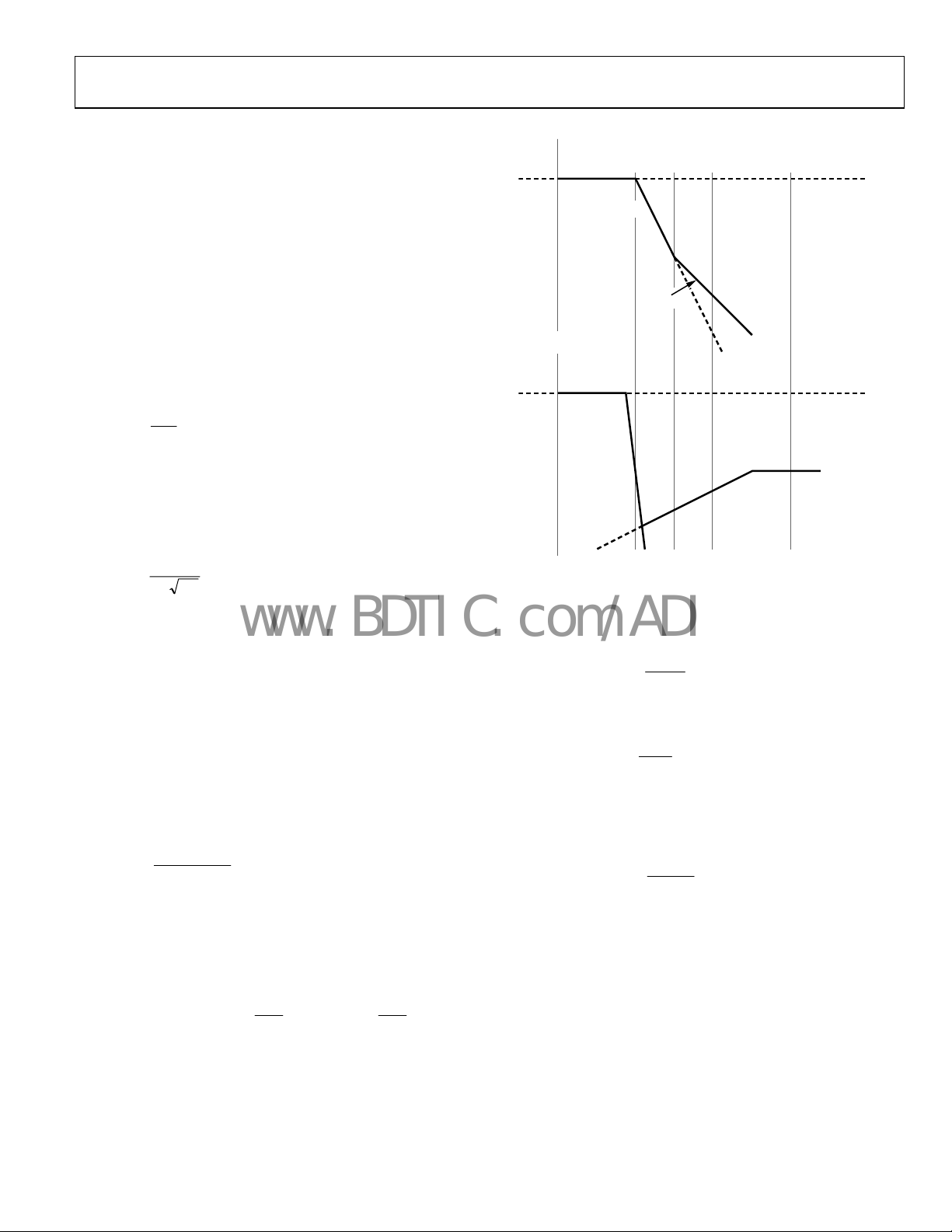
FILTER
A
FILTER
≈ fCO, add another 3 dB to account for the local difference
If f
ESR
ESR
×−=
⎟
⎜
f
LC
⎠
⎝
⎞
⎛
f
ESR
⎟
⎜
⎛
⎜
logdB20logdB40 (22)
×−
⎜
⎝
⎞
f
CO
⎟
⎟
f
ESR
⎠
The factor of 2 in the numerator takes into account that the
YNC frequency is divided by 2 to generate the switching
S
frequency. For example, if the FREQ pin is set high for the
600 kHz range and a 2 MHz SYNC signal is applied, the ramp
voltage is 0.78 V. The gain of the modulator is increased by
4.4 dB in this example.
between the exact solution and the linear approximation.
–20dB/dec
V
IN
V
RAMP
V
IN
3.1
V
⎛
2
f
FREQ
⎜
⎜
f
SYNC
⎝
f
SW
FREQUENCY
A
FILTER
Φ
FILTER
05936-025
⎞
⎟
⎟
⎠
⎞
⎟
⎟
⎠
⎞
⎟
(25)
⎟
⎠
Rev. D | Page 19 of 32
Page 20

ADP1823
www.BDTIC.com/ADI
The rest of the system gain is needed to reach 0 dB at crossover.
The total gain of the system, therefore, is given by
AT = A
MOD
+ A
FILTER
+ A
(26)
COMP
where:
A
is the gain of the PWM modulator.
MOD
A
is the gain of the LC filter including the effects of
FILTER
the ESR zero.
A
is the gain of the compensated error amplifier.
COMP
Additionally, the phase of the system must be brought back up
t
o guarantee stability. Note from the Bode plot of the filter that
the LC contributes −180° of phase shift. Additionally, because
the error amplifier is an integrator at low frequency, it contributes
an initial −90°. Therefore, before adding compensation or
accounting for the ESR zero, the system is already down −270°.
To avoid loop inversion at crossover, or −180° phase shift, a
good initial practical design is to require a phase margin of 60°,
which is therefore an overall phase loss of −120° from the initial
low frequency dc phase. The goal of the compensation is to
boost the phase back up from −270° to −120° at crossover.
Two common compensation schemes are used, which are
s
ometimes referred to as Type II or Type III compensation,
depending on whether the compensation design includes two
or three poles. (Dominant pole compensation, or single pole
compensation, is referred to as Type I compensation, but
unfortunately, it is not very useful for dealing successfully with
switching regulators.)
If the zero produced by the ESR of the output capacitor provides
s
ufficient phase boost at crossover, Type II compensation is
adequate. If the phase boost produced by the ESR of the output
capacitor is not sufficient, another zero is added to the compensation network, and thus Type III is used.
In Figure 27, the location of the ESR zero corner frequency
ives significantly different net phase at the crossover frequency.
g
Use the following guidelines for selecting between Type II and
ype III compensators:
T
f
≤ fCO/2, use Type II compensation.
If
ESRZ
f
> fCO/2, use Type III compensation.
If
ESRZ
LC FILTER BODE PLOT
PHASE CONTRIBUTI ON AT CROSSO VER
GAIN
PHASE
OF VARIOUS ESR ZERO CORNERS
f
f
0dB
0°
–90°
–180°
f
–40dB/dec
–20dB/dec
ESR2
ESR1
LC
Figure 27. LC Filter Bode Plot
ESR3
fCOf
Φ
1
Φ
Φ
f
SW
FREQUENCY
2
3
The following equations were used for the calculation of the
compensation components as shown in Figure 28 and Figure 29:
f
Z
f+=
Z
f+=
P
P
1
= (27)
1
2
1
2
CR
π2
I
Z
1
FF
TOP
1
CC
R
π2
= (30)
HFI
Z
CC
1
CRfπ2
FFFF
(28)
)(π2
RRC
FF
(29)
HFI
where:
is the zero produced in the Type II compensation.
f
Z1
f
is the zero produced in the Type III compensation.
Z2
is the pole produced in the Type II compensation.
f
P1
f
in the pole produced in the Type III compensation.
P2
05936-026
Rev. D | Page 20 of 32
Page 21

ADP1823
www.BDTIC.com/ADI
Type II Compensator
–
1
G
(dB)
PHASE
–180°
–270°
R
FROM
TOP
V
OUT
R
BOT
S
L
O
P
E
f
Z
C
R
Z
EA
HF
VREF
–
1
S
L
OP
E
f
P
C
I
COMP
TO PWM
VRAMP
0V
5936-027
Next choose the high frequency pole f
P
1
Because C
1
P
Solving for C
HF
Type III Compensator
Figure 28. Type II Compensation
If the output capacitor ESR zero frequency is sufficiently low
(≤½ of the crossover frequency), use the ESR to stabilize the
regulator. In this case, use the circuit shown in Figure 28.
C
alculate the compensation resistor, R
, with the following
Z
equation:
ffVR
TOP
R = (31)
Z
IN
COESRRAMP
2
fV
LC
FROM
V
OUT
where:
is chosen to be 1/10 of f
f
CO
V
is 1.3 V.
RAMP
Next choose the compensation capacitor to set the compensati
on zero, f
, to the lesser of ¼ of the crossover frequency or ½
Z1
of the LC resonant frequency.
ff
f
1
Z
SWCO
404
SW.
If the output capacitor ESR zero frequency is greater than half
of the crossover frequency, use a Type III compensator as
shown in Figure 29. Set the poles and zeros as follows:
1
=== (32)
CR
π2
I
Z
or
f
LC
f
Z
1
2
Solving for C
Solving for C
I
20
= (34)
I
Z
I
= (35)
I
Z
Use the larger value of C
1
== (33)
CR
π2
I
Z
or
in Equation 32 yields
1
fRCπ
SW
in Equation 33 yields
1
fRCπ
LC
from Equation 34 or Equation 35.
I
Use the lower zero frequency from Equation 40 or Equation 41.
C
alculate the compensator resistor, R
R =
Z
Next calculate C
Because of the finite output current drive of the error amplifier,
C
needs to be less than 10 nF. If it is larger than 10 nF, choose a
I
larger R
and recalculate RZ and CI until CI is less than 10 nF.
TOP
C =
I
1
ff
= (36)
SW
2
<< CI, Equation 29 is simplified to
HF
1
=
= (38)
PHASE
(37)
CRfπ2
HF
Z
in Equation 36 and Equation 37 yields
HF
1
RfCπ
SW
Z
–
1
G
S
L
(dB)
–90°
–270°
R
FF
R
TOP
R
BOT
O
S
P
E
1
+
f
Z
C
HF
R
C
Z
FF
EA
VREF
Figure 29. Type III Compensation
1
fff
== (39)
PP
21
SW
2
ff
ff
21
ZZ
ff
2
ZZ
RAMP
TOP
IN
.
I
1
π2
fR
ZZ
SWCO
==== (40)
404
f
LC
2
1
===
CR
π
2
I
Z
ffVR
CO
1
Z
(42)
2
fV
LC
(43)
1
to be half of fSW.
P1
E
P
LO
–
1
S
L
O
P
E
f
P
C
I
COMP
TO PWM
VRAMP
0V
5936-028
1
CR
π2
I
Z
(41)
.
Z
Rev. D | Page 21 of 32
Page 22

ADP1823
V
www.BDTIC.com/ADI
Because of the finite output current drive of the error amplifier,
needs to be less than 10 nF. If it is larger than 10 nF, choose a
C
I
larger R
Because C
Next calculate the feedforward capacitor, C
R
TOP
Solving C
where f
The feedforward resistor, R
and recalculate RZ and CI until CI is less than 10 nF.
TOP
<< CI, combining Equation 29 and Equation 39 yields
HF
1
= (44)
HF
SW
RfCπ
Z
. Assuming RFF <<
FF
, then Equation 28 is simplified to
1
=
2
Z
in Equation 45 yields
FF
= (46)
FF
2
is obtained from Equation 40 or Equation 41.
Z2
(45)
RCfπ2
FF
TOP
1
fRCπ
2
ZTOP
, can be calculated by combining
FF
Equation 30 and Equation 39.
FF
fCRπ
FF
SW
1
= (47)
Check that the calculated component values are reasonable. For
i
nstance, capacitors smaller than about 10 pF should be avoided.
In addition, the ADP1823 error amplifier has finite output
current drive; therefore, R
values less than 3 k and CI values
Z
greater than 10 nF should be avoided. If necessary, recalculate the
compensation network with a different starting value of R
is too small and CI is too big, start with a larger value of R
R
Z
TOP
. If
TOP
This compensation technique should yield a good working
solution.
In general, aluminum electrolytic capacitors have high ESR;
t
herefore, a Type II compensation is adequate. However, if several
aluminum electrolytic capacitors are connected in parallel,
producing a low effective ESR, Type III compensation is needed. In
addition, ceramic capacitors have very low ESR, on the order of
a few milliohms; therefore, Type III compensation is needed for
ceramic output capacitors. Type III compensation offers better
performance than Type II in terms of more low frequency gain
and more phase margin and less high frequency gain at the
crossover frequency.
SOFT START
The ADP1823 uses an adjustable soft start to limit the output
voltage ramp-up period, thus limiting the input inrush current.
The soft start is set by selecting the capacitor, C
SS2 to GND. The ADP1823 charges C
to 0.8 V through an
SS
internal 90 k resistor. The voltage on the soft start capacitor
while it is charging is
t
⎞
RC
SS
⎟
(48)
eV 1V8.0
−=
⎟
⎠
CSS
⎛
⎜
⎜
⎝
, from SS1 and
SS
.
The soft start period ends when the voltage on the soft start pin
eaches 0.6 V. Substituting 0.6 V for V
r
and solving for the
SS
number of RC time constants
t
SS
⎛
⎜
1V8.0V6.0
e (49)
−=
⎜
⎝
= 1.386 RCSS (50)
t
SS
⎞
)(k90
C
SS
⎟
⎟
⎠
Because R = 90 k,
C
= tSS × 8 µF/s (51)
SS
where t
is the desired soft start time in seconds.
SS
VOLTAGE TRACKING
The ADP1823 includes a tracking feature that prevents an
output voltage from exceeding a master voltage. This feature is
especially important when the ADP1823 is powering separate
power supply voltages on a single integrated circuit, such as the
core and I/O voltages of a DSP or microcontroller. In these
cases, improper sequencing can cause damage to the load.
The ADP1823 tracking input is an additional positive input to
he error amplifier. The feedback voltage is regulated to the lower of
t
the 0.6 V reference or the voltage at TRK; therefore, a lower
voltage on TRK limits the output voltage. This feature allows
implementation of two different types of tracking: coincident
tracking, where the output voltage is the same as the master
voltage until the master voltage reaches regulation, or ratiometric
tracking, where the output voltage is limited to a fraction of the
master voltage.
In all tracking configurations, the master voltage should be
her than the slave voltage.
hig
Note that the soft start time setting of the master voltage should
b
e longer than the soft start of the slave voltage. This forces the
rise time of the master voltage to be imposed on the slave voltage.
If the soft start setting of the slave voltage is longer, the slave
comes up more slowly and the tracking relationship is not seen
at the output. The slave channel should still have a soft start
capacitor to give a small but reasonable soft start time to protect
in case of a restart after a current-limit event.
OUT
R
ERROR
AMPLIFIER
COMP
FB
TRK
0.6V
SS
DETAIL VIEW OF
ADP1823
Figure 30. Voltage Tracking
R
R
TRKT
TRKB
TOP
R
BOT
MASTER
VOLTAGE
05936-029
Rev. D | Page 22 of 32
Page 23
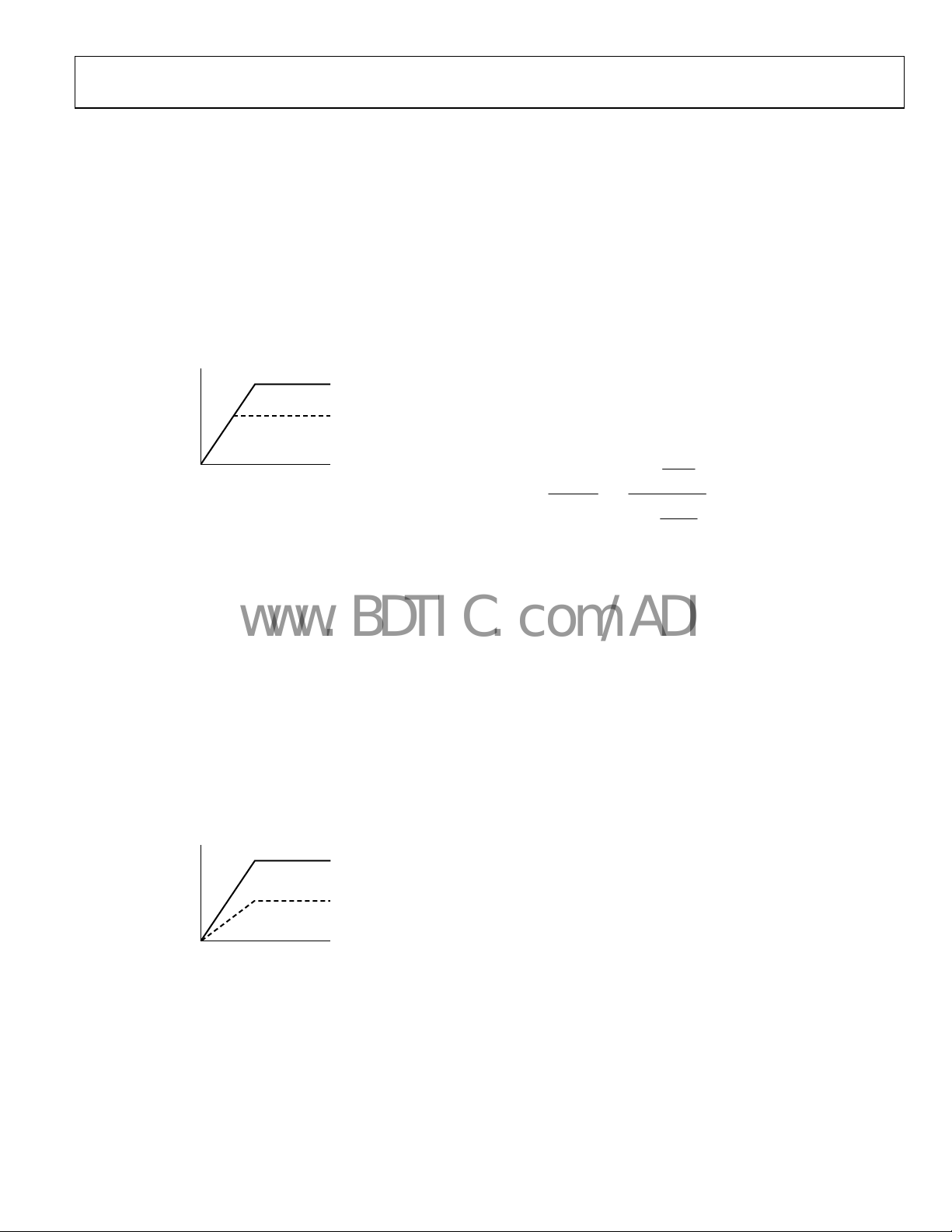
ADP1823
www.BDTIC.com/ADI
COINCIDENT TRACKING
The most common application is coincident tracking, used
in core vs. I/O voltage sequencing and similar applications.
Coincident tracking limits the slave output voltage to be the
same as the master voltage until it reaches regulation. Connect
the slave TRK input to a resistor divider from the master voltage
that is the same as the divider used on the slave FB pin. This
technique forces the slave voltage to be the same as the master
voltage.
For coincident tracking, use R
where R
TOP
and R
are the values chosen in the
BOT
TRKT
the Voltage Mode Buck Regulator
MASTER VOLTAGE
SLAVE VOLTAGE
VOLTAGE
TIME
Figure 31. Coincident Tracking
TOP
section.
and R
= RB
TRKB
BOT
Compensating
05936-030
,
= R
As the master voltage rises, the slave voltage rises identically.
Eventually, the slave voltage reaches its regulation voltage,
where the internal reference takes over the regulation while the
TRK input continues to increase and thus removes itself from
influencing the output voltage. To ensure that the output voltage
accuracy is not compromised by the TRK pin being too close in
voltage to the 0.6 V reference, make sure that the final value of
the master voltage is greater than the slave regulation voltage by
at least 10%, or 60 mV as seen at the FB node. The higher the
final value, the better the performance is. A difference of 60 mV
between TRK and the 0.6 V reference produces about 3 mV of
offset in the error amplifier, or 0.5%, at room temperature, while
100 mV between them produces only 0.6 mV or 0.1% offset.
RATIOMETRIC TRACKING
Ratiometric tracking limits the slave output voltage to a fraction
of the master voltage. For example, the termination voltage for
DDR memories, VTT, is set to half the VDD voltage.
MASTER VOLTAGE
For ratiometric tracking, the simplest configuration is to tie the
TRK pin of the slave channel to the FB pin of the master channel.
This has the advantage of having the fewest components, but
the accuracy suffers as the TRK pin voltage becomes equal to
the internal reference voltage and an offset is imposed on the
error amplifier of about −18 mV at room temperature.
A more accurate solution is to provide a divider from the
ter voltage that sets the TRK pin voltage to be something
mas
lower than 0.6 V at regulation, for example, 0.5 V. The slave
channel can be viewed as having a 0.5 V external reference
supplied by the master voltage.
Once this is complete, the FB divider for the slave voltage is
ned as in the Compensating the Voltage Mode Buck
desig
lator section, except to substitute the 0.5 V reference for
Regu
voltage. The ratio of the slave output voltage to the
th
e V
FB
master voltage is a function of the two dividers:
V
V
MASTER
OUT
⎛
⎜
+
1
⎜
⎝
=
⎛
⎜
1
+
⎜
⎝
R
R
R
R
⎞
TOP
⎟
⎟
BOT
⎠
(52)
⎞
TRKT
⎟
⎟
TRKB
⎠
Another option is to add another tap to the divider for the
ter voltage. Split the R
mas
resistor of the master voltage into
BOT
two pieces, with the new tap at 0.5 V when the master voltage is
in regulation. This technique saves one resistor, but be aware
that Type III compensation on the master voltage causes the
feedforward signal of the master voltage to appear at the TRK
input of the slave channel.
By selecting the resistor values in the divider carefully, Equation 52
hows that the slave voltage output can be made to have a faster
s
ramp rate than that of the master voltage by setting the TRK
voltage at the slave larger than 0.6 V and R
. Make sure that the master SS period is long enough (that
R
TRKT
greater than
TRKB
is, sufficiently large SS capacitor) such that the input inrush
current does not run into the current limit of the power supply
during startup.
SLAVE VOLTAGE
VOLTAGE
TIME
Figure 32. Ratiometric Tracking
5936-031
Rev. D | Page 23 of 32
Page 24

ADP1823
(
)
(
)
www.BDTIC.com/ADI
Setting the Channel 2 Undervoltage Threshold for Ratiometric Tracking
If FB2 is regulated to a voltage lower than 0.6 V by configuring
RK2 for ratiometric tracking, the Channel 2 undervoltage
T
threshold can be set appropriately by splitting the top resistor
in the voltage divider, as shown in Figure 33. R
is the same as
BOT
calculated for the compensation in Equation 52, and
R
= RA + RB (53)
TOP
POK2
Figure 33. Setting the Channel 2 Undervoltage Threshold
B
TO ERROR
AMPLIFI ER
550mV
750mV
CHANNEL 2
OUTPUT
VOLTAGE
UV2
FB2
R
A
R
B
R
BOT
05936-032
The current in all the resistors is the same.
VV
V
2
FB
R
BOT
−
22
FBUV
= (54)
R
=
B
OUT
VV
−
2
UV
2
R
A
where:
is 600 mV.
V
UV2
V
is the feedback voltage value set during the ratiometric
FB2
tracking calculations.
is the Channel 2 output voltage.
V
OUT2
Solving for R
and RB, B
A
VV
2
UV
2
OUTA
RR−=
A
BOT
=
B
BOT
V
FB
VVRR−
V
2
FB
(55)
2
22
FBUV
(56)
THERMAL CONSIDERATIONS
The current required to drive the external MOSFETs comprises
the vast majority of the power dissipation of the ADP1823. The
on-chip LDO regulates down to 5 V, and this 5 V supplies the
drivers. The full gate drive current passes through the LDO and
is then dissipated in the gate drivers. The power dissipated on
the gate drivers on the ADP1823 is
P
= V
D
IN fSW(QDH1
where:
is the voltage applied to IN.
V
IN
is the switching frequency.
f
SW
Q numbers are the total gate charge specifications from the
selected MOSFET data sheets.
The power dissipation heats the ADP1823. As the switching
f
requency, the input voltage, and the MOSFET size increase, the
power dissipation on the ADP1823 increases. Care must be taken
not to exceed the maximum junction temperature. To calculate
the junction temperature from the ambient temperature and
power dissipation
= TA + PD θJA (58)
T
J
The thermal resistance, θ
depending on board layout, and the maximum specified junction
temperature is 125°C, which means that at a maximum ambient
temperature of 85°C without airflow, the maximum dissipation
allowed is about 1 W.
A thermal shutdown protection circuit on the ADP1823 shuts
o
ff the LDO and the controllers if the die temperature exceeds
approximately 145°C, but this is a gross fault protection only
and should not be relied upon for system reliability.
+ Q
+ Q
+ Q
DL1
DH2
, of the package is typically 40°C/W
JA
) (57)
DL2
Rev. D | Page 24 of 32
Page 25

ADP1823
www.BDTIC.com/ADI
PCB LAYOUT GUIDELINES
In any switching converter, some circuit paths carry high dI/dt,
which can create spikes and noise. Other circuit paths are
sensitive to noise. Still others carry high dc current and can
produce significant IR voltage drops. The key to proper PCB
layout of a switching converter is to identify these critical paths
and arrange the components and copper area accordingly.
When designing PCB layouts, be sure to keep high current
loops small. In addition, keep compensation and feedback
components away from the switch nodes and their associated
components.
The following is a list of recommended layout practices for the
AD
P1823, arranged by decreasing order of importance.
The current waveform in the top and bottom FETs is a pulse
•
with very high dI/dt; therefore, the path to, through, and from
each individual FET should be as short as possible and the
two paths should be commoned as much as possible. In
designs that use a pair of D-Pak or SO-8 FETs on one side
of the PCB, it is best to counter-rotate the two so that the
switch node is on one side of the pair and the high-side
drain can be bypassed to the low-side source with a suitable
ceramic bypass capacitor, placed as close as possible to the
FETs to minimize inductance around this loop through the
FETs and capacitor. The recommended bypass ceramic
capacitor values range from 1 F to 22 F depending upon
the output current. This bypass capacitor is usually connected
to a larger value bulk filter capacitor and should be grounded to
the PGND plane.
•
GND, the VREG bypass, the soft start capacitor, and the
bottom end of the output feedback divider resistors should
be tied to an (almost isolated) small AGND plane. All of
these connections should have connections from the pin
to the AGND plane that are as short as possible. No high
current or high dI/dt signals should be connected to
this AGND plane. The AGND area should be connected
through one wide trace to the negative terminal of the
output filter capacitors.
The PGND pin handles high dI/dt gate drive current
•
returning from the source of the low-side MOSFET. The
voltage at this pin also establishes the 0 V reference for the
overcurrent limit protection (OCP) function and the CSL
pin. A small PGND plane should connect the PGND pin
and the PVCC bypass capacitor through a wide and direct
path to the source of the low-side MOSFET. The placement
is critical for controlling ground bounce. The negative
of C
IN
terminal of C
the low-side MOSFET.
needs to be placed very close to the source of
IN
Avoid long traces or large copper areas at the FB and CSL
•
pins, which are low signal level inputs that are sensitive to
capacitive and inductive noise pickup. It is best to position
any series resistors and capacitors as close as possible to
these pins. Avoid running these traces close and parallel to
high dI/dt traces.
•
The switch node is the noisiest place in the switcher circuit
with large ac and dc voltage and current. This node should
be wide to minimize resistive voltage drop. However, to
minimize the generation of capacitively coupled noise, the
total area should be small. Place the FETs and inductor all
close together on a small copper plane to minimize series
resistance and keep the copper area small.
•
Gate drive traces (DH and DL) handle high dI/dt and,
therefore, they tend to produce noise and ringing. They
should be as short and direct as possible. If possible, avoid
using feedthrough vias in the gate drive traces. If vias are
needed, it is best to use two relatively large ones in parallel
to reduce the peak current density and the current in each
via. If the overall PCB layout is less than optimal, slowing
down the gate drive slightly can be very helpful to reduce
noise and ringing. It is occasionally helpful to place small
value resistors (such as 5 or 10 Ω) in series with the gate
leads, mainly DH traces to the high-side FET gates. These
can be populated with 0 resistors if resistance is not
needed. Note that the added gate resistance increases the
switching rise and fall times and that in turn increases the
switching power loss in the MOSFET.
The negative terminal of output filter capacitors should be
•
tied closely to the source of the low-side FET. Doing this
helps to minimize voltage difference between GND and
PGND at the ADP1823.
•
Generally, be sure that all traces are sized according to the
current to be handled as well as their sensitivity in the
circuit. Standard PCB layout guidelines mainly address
heating effects of current in a copper conductor. These are
completely valid, but they do not fully cover other concerns,
such as stray inductance or dc voltage drop. Any dc voltage
differential in connections between ADP1823 GND and the
converter power output ground can cause a significant
output voltage error, because it affects converter output
voltage according to the ratio with the 600 mV feedback
reference. For example, a 6 mV offset between ground on the
ADP1823 and the converter power output causes a 1% error
in the converter output voltage.
Rev. D | Page 25 of 32
Page 26

ADP1823
www.BDTIC.com/ADI
The paste mask for the thermal pad needs to be designed for
LFCSP CONSIDERATIONS
The LFCSP has an exposed die paddle on the bottom that
efficiently conducts heat to the PCB. To achieve the optimum
performance from the LFCSP, give special consideration to the
layout of the PCB. Use the following layout guidelines for the
LFCSP:
The pad pattern is given in Figure 36. The pad dimension
•
should be followed closely for reliable solder joints while
maintaining reasonable clearances to prevent solder
bridging.
The thermal pad of the LFCSP provides a low thermal
•
impedance path to the PCB. Therefore, the PCB must be
properly designed to effectively conduct the heat away from
the package. This is achieved by adding thermal vias to the
PCB, which provide a thermal path to the inner or bottom
layers. See
t
hat the via diameter is small, which prevents the solder
from flowing through the via and leaving voids in the
thermal pad solder joint.
Note that the thermal pad is attached to the die substrate;
t
herefore, the planes that the thermal pad is connected to
must be electrically isolated or connected to GND.
The solder mask opening should be about 120 microns
•
(4.7 mils) larger than the pad size, resulting in a minimum
60 microns (2.4 mils) clearance between the pad and the
solder mask.
Figure 36 for the recommended via pattern. Note
•
the maximum coverage to effectively remove the heat from
the package. However, due to the presence of thermal vias
and the large size of the thermal pad, eliminating voids may
not be possible. In addition, if the solder paste coverage is
too large, solder joint defects may occur. Therefore, it is
recommended to use multiple small openings over a single
big opening in designing the paste mask. The recommended
paste mask pattern is given in
out 80% coverage, which should not degrade the
in ab
thermal performance of the package significantly.
The recommended paste mask stencil thickness is 0.125 mm.
•
A laser cut stainless steel stencil with trapezoidal walls
should be used.
A no-clean, Type 3 solder paste should be used for mounting
•
the LFCSP. In addition, a nitrogen purge during the reflow
process is recommended.
The package manufacturer recommends that the reflow
•
temperature should not exceed 220°C and the time above
liquid is less than 75 seconds. The preheat ramp should be
3°C per second or lower. The actual temperature profile
depends on the board density; the assembly house must
determine what works best.
Figure 36. This pattern results
The paste mask opening is typically designed to match the
•
pad size used on the peripheral pads of the LFCSP. This
technique should provide a reliable solder joint as long as
the stencil thickness is about 0.125 mm.
Rev. D | Page 26 of 32
Page 27

ADP1823
V
www.BDTIC.com/ADI
APPLICATION CIRCUITS
The ADP1823 controller can be configured to regulate outputs
with loads of more than 20 A if the power components, such as
the inductor, MOSFETs, and the bulk capacitors, are chosen
carefully to meet the power requirement. The maximum load
and power dissipation are limited by the powertrain components.
Figure 1 shows a typical application circuit that can drive an
output
load of 8 A.
Figure 34 shows an application circuit that can drive 20 A loads.
N
ote that two low-side MOSFETs are needed to deliver the 20 A
load. The bulk input and output capacitors used in this example
are Sanyo OS-CON capacitors, which have low ESR and high
current ripple rating. An alternative to the OS-CON capacitors
are the polymer aluminum capacitors that are available from
other manufacturers, such as United Chemi-Con. Aluminum
electrolytic capacitors, such as the Rubycon ZLG low-ESR series,
IN = 5.5
TO 20V
can also be paralleled up at the input or output to meet the
r
ipple current requirement. Because the aluminum electrolytic
capacitors have higher ESR and much larger variation in
capacitance over the operating temperature range, a larger bulk
input and output capacitance is needed to reduce the effective
ESR and suppress the current ripple.
p
olymer aluminum or the aluminum electrolytic capacitors can
Figure 34 shows that the
be used at the outputs.
1.2V, 20A
C
OUT2
820µF
25V
1µF
C
IN2
1µF
180µF
20V
L2
1µH
5600pF
1µF
×2
390Ω
2kΩ
2kΩ
M5
M6
f
OSC
M1, M4: IRL R7807Z
L1, L2: TOKO, FDA1254-1ROM
C
OUT1
D2
0.47µF
M4
2kΩ
120nF
10kΩ
4.7nF
= 300kHz
: SANYO, 2R5S EPC820M
PV IN
TRK1
TRK2
VREG
BST1
DH1
ADP1823
SW1
CSL1
DL1
PGND1
FB1
COMP1
GND
AGND
EN1
EN2
BST2
DH2
SW2
CSL2
DL2
PGND2
FB2
COMP2
FREQ
LDOSD
SYNC
D1, D2: VISH AY, BAT54
M2, M3, M5, M6: IRFR3709Z
C
C
D1
0.47µF
2kΩ
1.5nF
47kΩ
6.8nF
, C
: SANYO, 20SP180M
IN1
IN2
: RUBYCON, 6.3Z LG1200M10×16
OUT2
M1
M2
1µF
PGND
C
IN1
180µF
20V
L1
1µH
M3
2kΩ
1kΩ
10nF
200Ω
1µF
1.8V, 20A
C
OUT1
1200µF
6.3V
×3
05936-033
Figure 34. Application Circuit with 20 A Output Loads
Rev. D | Page 27 of 32
Page 28

ADP1823
V
www.BDTIC.com/ADI
The ADP1823 can also be configured to drive an output load of
less than 1 A. Figure 35 shows a typical application circuit that
ives 1.5 A and 3 A loads in all multilayer ceramic capacitor
dr
(MLCC) solutions. Notice that the two MOSFETs used in this
example are dual-channel MOSFETs in a PowerPAK® SO-8
package, which reduces cost and saves layout space. An alternative
to using the dual-channel SO-8 package is using two single
MOSFETs in SOT-23 or TSOP-6 packages, which are low cost
and small in size.
TO 5V
IN = 3.7
1.0V, 3A
C
OUT3
100µF
C
OUT2
47µF
1µF
10µF
1µF
×2
2.2µH
8.2nF
1µF
84.5Ω
f
OSC
M1 TO M4: DUAL-CHANNE L SO-8 IRF7331
L2: TOKO, FDV0602-2R2M
C
OUT2
1.33kΩ
2kΩ
= 600kHz
: MURATA, GRM31CR60J476M
0.22µF
M3
L2
M4
6.65kΩ
D2
4.12kΩ
1.5nF
PV IN
TRK1
TRK2
VREG
BST1
DH1
EN1
EN2
BST2
DH2
ADP1823
SW1
CSL1
DL1
PGND1
FB1
COMP1
GND
SW2
CSL2
DL2
PGND2
FB2
COMP2
FREQ
LDOSD
SYNC
AGND
L1: SUMIDA, CDRH5D28-2R5NC
, C
C
OUT1
OUT3
D1, D2: VISHAY BAT54
2.5µH
M2
1µF
L1
PGND
2kΩ
10µF
×2
1kΩ
8.2nF
84.5Ω
D1
0.22µF
M1
1.4kΩ
120nF120nF
6.65kΩ
1.5nF
IN
: MURATA, GRM31CR60J107M
1µF 10µF
1.8V, 1.5A
C
OUT1
100µF
05936-034
Figure 35. Application Circuit with All Multilayer Ceramic Capacitors (MLCC)
Rev. D | Page 28 of 32
Page 29
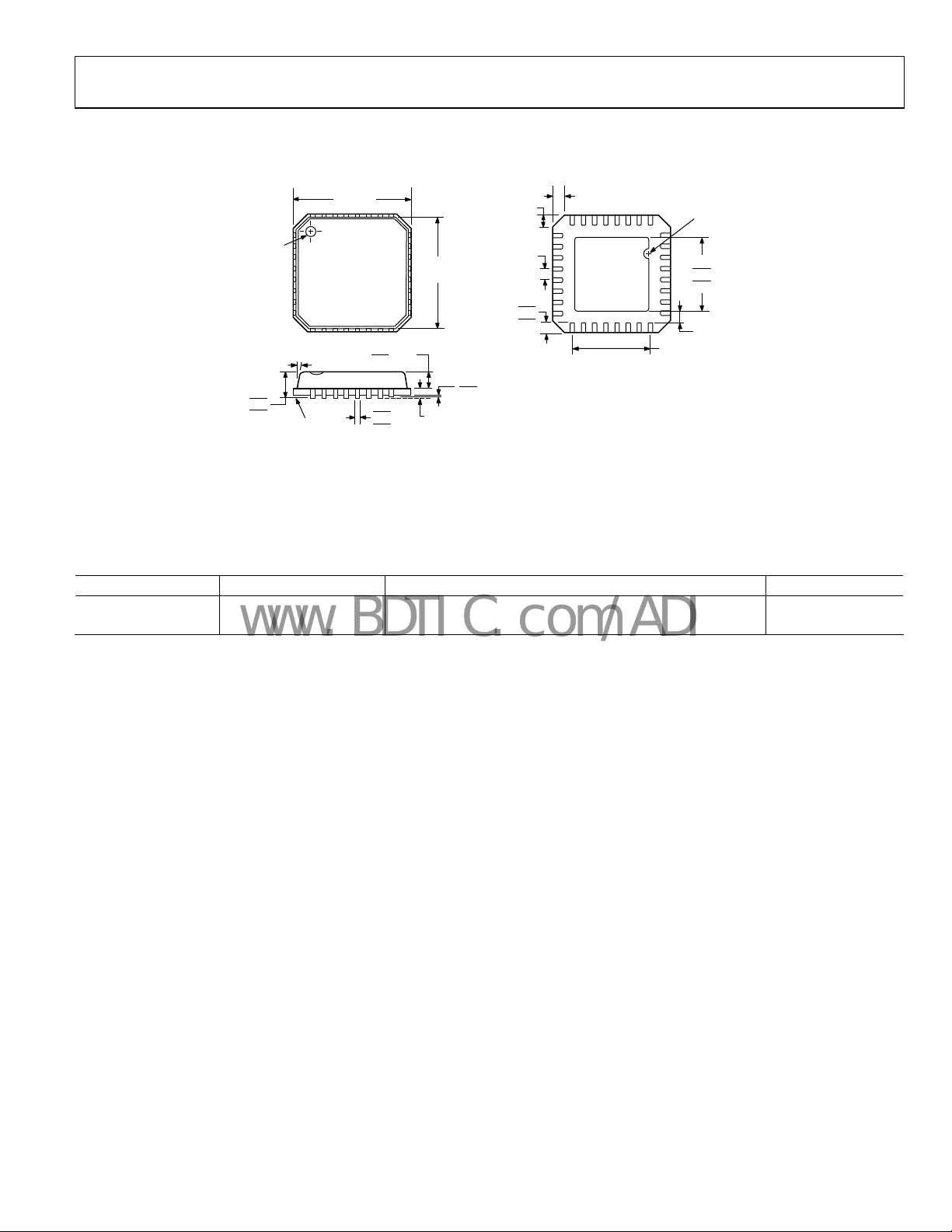
ADP1823
www.BDTIC.com/ADI
OUTLINE DIMENSIONS
0.08
0.60 MAX
25
24
EXPOSED
PAD
(BOTTOM VIEW)
17
16
32
1
8
9
3.50 REF
PIN 1
INDICATOR
3.25
3.10 SQ
2.95
0.25 MIN
5.00
PIN 1
INDICATOR
1.00
0.85
0.80
12° MAX
SEATING
PLANE
BSC SQ
TOP
VIEW
0.80 MAX
0.65 TYP
0.30
0.23
0.18
COMPLIANT TO JEDEC STANDARDS MO-220-VHHD-2
4.75
BSC SQ
0.20 REF
0.05 MAX
0.02 NOM
0.60 MAX
0.50
BSC
0.50
0.40
0.30
COPLANARITY
Figure 36. 32-Lead Lead Frame Chip Scale Package [LFCSP_VQ]
5
mm × 5 mm Body, Very Thin Quad
(CP-32-2)
Dimensions shown in millimeters
ORDERING GUIDE
Model Temperature Range
ADP1823ACPZ-R7
2
−40°C to +85°C 32-Lead Lead Frame Chip Scale Package [LFCSP_VQ] CP-32-2
ADP1823-EVAL Evaluation Board
1
Operating junction temperature is −40°C to +125°C.
2
Z = RoHS Compliant Part.
1
Package Description Package Option
Rev. D | Page 29 of 32
Page 30

ADP1823
www.BDTIC.com/ADI
NOTES
Rev. D | Page 30 of 32
Page 31

ADP1823
www.BDTIC.com/ADI
NOTES
Rev. D | Page 31 of 32
Page 32

ADP1823
www.BDTIC.com/ADI
NOTES
©2006–2007 Analog Devices, Inc. All rights reserved. Trademarks and
registered trademarks are the property of their respective owners.
D05936-0-10/07(D)
Rev. D | Page 32 of 32
 Loading...