

Page 1
www.BDTIC.com/ADI
Step-Down DC-to-DC Controller
FEATURES
Wide power-input voltage range: 1 V to 24 V
Chip supply voltage range: 3.7 V to 5.5 V
Wide output voltage range: 0.6 V to 85% of input voltage
1% accuracy, 0.6 V reference voltage
All N-channel MOSFET design for low cost
Fixed-frequency operation 300 kHz, 600 kHz, or
synchr
onized operation up to 1.2 MHz
No current sense resistor required
Power-good output
Programmable soft start with reverse current protection
Soft start, thermal overload, current-limit protection
Undervoltage lockout
10 μA shutdown supply current
Small, 16-lead QSOP
APPLICATIONS
Telecommunications and networking systems
Set-top boxes
Printers
Servers
Medical imaging systems
Microprocessor and DSP core power supplies
Mobile communication base stations
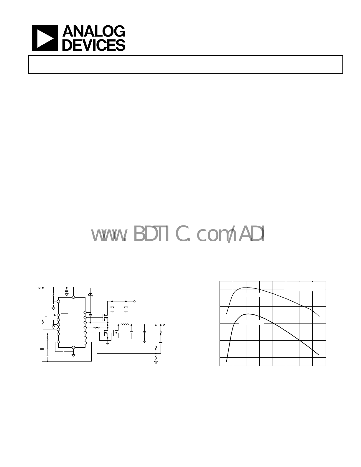
BIAS INPUT
5V
100kΩ
1.5nF
f
C
C
L1: COILTRONICS, HC7-1R0
1µF
10Ω
PVCC
VCC
1µF
= 300kHz
SW
IN2
OUT2
ADP1821
SHDN
FREQ
SYNC
PWGD
COMP
4.7kΩ
SS
GND
100nF
6.8nF
: SANYO, OSCON 20SP180M
: SANYO, OSCON 2R5SEPC820M
AGND
Figure 1. Typical Operating Circuit
BST
CSL
PGND
D1
0.47µF
DH
SW
3.3kΩ
DL
FB
C
: MURATA, GRM31MR71E225k
IN1
M1: IRLR7807Z
M2, M3: IRFR3709Z
D1: VISHAY BAT54
C
IN1
+
2.2µF
25V
M1
M2 M3
POWER INPUT
2.5V TO 20V
+
L1 = 1µH
C
IN2
2.2µF
25V
×2
C
10µF
6.3V
×2
OUT1
OUTPUT
1.8V, 20A
C
OUT2
+
820µF
2.5V
×2
2kΩ
1kΩ
300Ω
10nF
ADP1821
GENERAL DESCRIPTION
The ADP1821 is a versatile and inexpensive, synchronous,
pulse-width-modulated (PWM), voltage-mode, step-down
controller. It drives an all N-channel power stage to regulate an
output voltage as low as 0.6 V. The ADP1821 can be configured
to provide output voltages from 0.6 V to 85% of the input
voltage and is sized to handle large MOSFETs for point-of-load
regulators.
The ADP1821 is well suited for a wide range of high power
pplications, such as DSP and processor core power in telecom-
a
munications, medical imaging, high performance servers, and
industrial applications. It operates from a 3.7 V to 5.5 V supply
with a power input voltage ranging from 1.0 V to 24 V.
The ADP1821 operates at a pin-selectable, fixed switching
requency of either 300 kHz or 600 kHz, minimizing external
f
component size and cost. For noise sensitive applications, it
can be synchronized to an external clock to achieve switching
frequencies between 300 kHz and 1.2 MHz. The ADP1821
includes soft start protection to limit the inrush current from
the input supply during startup, reverse current protection
during soft start for precharged outputs, as well as a unique
adjustable lossless current-limit scheme utilizing external
MOSFET sensing.
The ADP1821 operates over the –40°C to +125°C junction
emperature range and is available in a 16-lead QSOP.
t
97
96
95
94
93
92
91
EFFICIENCY (%)
90
89
88
87
5310-001
0
3.3V OUTPUT
1.8V OUTPUT
2 4 6 8 10 12 14
LOAD CURRENT (A)
Figure 2. Efficiency vs. Load Current, 5 V Input
TA = 25°C
FREQUENCY = 300kHz
16
05310-002
Rev. C
Information furnished by Analog Devices is believed to be accurate and reliable. However, no
responsibility is assumed by Anal og Devices for its use, nor for any infringements of patents or ot her
rights of third parties that may result from its use. Specifications subject to change without notice. No
license is granted by implication or otherwise under any patent or patent rights of Analog Devices.
Trademarks and registered trademarks are the property of their respective owners.
One Technology Way, P.O. Box 9106, Norwood, MA 02062-9106, U.S.A.
Tel: 781.329.4700 www.analog.com
Fax: 781.461.3113 ©2005–2007 Analog Devices, Inc. All rights reserved.
Page 2

ADP1821
www.BDTIC.com/ADI
TABLE OF CONTENTS
Features.............................................................................................. 1
Applications....................................................................................... 1
General Description ......................................................................... 1
Revision History ............................................................................... 2
Specifications..................................................................................... 3
Absolute Maximum Ratings............................................................ 5
ESD Caution.................................................................................. 5
Simplified Block Diagram ........................................................... 5
Pin Configuration and Function Descriptions............................. 6
Typical Performance Characteristics ............................................. 7
Theory of Operation ........................................................................ 9
Soft Start ........................................................................................ 9
Error Amplifier............................................................................. 9
Current-Limit Scheme................................................................. 9
MOSFET Drivers........................................................................ 10
Input Voltage Range ................................................................... 10
Setting the Output Voltage........................................................ 10
Switching Frequency Control and Synchronization.............. 10
Compensation............................................................................. 11
Power-Good Indicator............................................................... 11
Thermal Shutdown .................................................................... 11
Shutdown Control...................................................................... 11
Application Information................................................................ 12
Selecting the Input Capacitor................................................... 12
Output LC Filter......................................................................... 12
Selecting the MOSFETs ............................................................. 13
Setting the Current Limit.......................................................... 14
Feedback Voltage Divider ......................................................... 14
Compensating the Voltage Mode Buck Regulator................. 14
Setting the Soft Start Period...................................................... 18
PCB Layout Guideline ................................................................... 19
Recommended Component Manufacturers........................... 20
Application Circuits ....................................................................... 21
Outline Dimensions....................................................................... 23
Ordering Guide .......................................................................... 23
REVISION HISTORY
4/07—Rev. B to Rev. C
Changes to Specifications Section.................................................. 3
Changes to Absolute Maximum Ratings Section......................... 5
Changes to Current-Limit Scheme Section ................................ 10
Changes to Setting the Current Limit Section............................ 14
Added Figure 15.............................................................................. 14
Changes to Compensating the Voltage Mode Buck
Regu
lator Section............................................................................ 15
Changes to Type II Compensator Section................................... 17
Changes to Type III Compensator Section ................................. 18
Changes to Application Circuits Section..................................... 21
Changes to Figure 22...................................................................... 21
Changes to Ordering Guide.......................................................... 23
12/06—Rev. A to Rev. B
Updated Format..................................................................Universal
C
hanges to Features Section............................................................ 1
Changes to Applications Section .................................................... 1
Changes to General Description Section ...................................... 1
Changes to Error Amplifier............................................................. 3
Changes to PWM Controller.......................................................... 3
Changes to Oscillator Frequency.................................................... 3
Changes to Theory of Operation Section.......................................9
Changes to Application Information Section............................. 12
Added PCB Layout Section........................................................... 19
Changes to Application Circuits Section..................................... 21
Added Summary of Equations Section........................................ 23
1/06—Rev. 0 to Rev. A
C
hanges to Specifications Table ......................................................3
Changes to Theory of Operation Section.................................... 10
Changes to Input Voltage Range Section .................................... 11
Added Equation 1........................................................................... 12
Changes to Equation 7 and Equation 8 ....................................... 13
Added Equation 9........................................................................... 13
Changes to Equation 16................................................................. 14
Changes to Figure 15...................................................................... 14
Changes to Equation 21................................................................. 15
Changes to Figure 16...................................................................... 15
Changes to Equation 28................................................................. 15
Updated Outline Dimensions....................................................... 18
7/05—Revision 0: Initial Version
Rev. C | Page 2 of 24
Page 3
ADP1821
www.BDTIC.com/ADI
SPECIFICATIONS
V
= V
VCC
statistical quality control (SQC). T
Table 1.
Parameter Conditions Min Typ Max Unit
POWER SUPPLY
Input Voltage 3.7 5.5 V
Undervoltage Lockout Threshold V
Undervoltage Lockout Threshold V
Undervoltage Lockout Hysteresis V
Quiescent Current I
Shutdown Current
Power Stage Supply Voltage 1.0 24 V
ERROR AMPLIFIER
FB Regulation Voltage TJ = −40°C to +85°C 594 600 606 mV
FB Regulation Voltage TJ = −40°C to +125°C 588 600 606 mV
FB Input Bias Current −100 +1 +100 nA
Error Amplifier Open-Loop Voltage Gain 70 dB
COMP Output Sink Current 600 A
COMP Output Source Current 110 A
COMP Clamp High Voltage 2.4 V
COMP Clamp Low Voltage 0.75 V
PWM CONTROLLER
PWM Peak Ramp Voltage 1.25 V
DL Minimum On Time FREQ = VCC (300 kHz) 120 170 220 ns
DL Minimum On-Time FREQ = VCC (300 kHz), TA = 25°C 140 170 200 ns
DH Maximum Duty Cycle FREQ = GND (300 kHz) 85 90 %
DH Minimum Duty Cycle FREQ = GND (300 kHz) 1 3 %
SOFT START
SS Pull-Up Resistance SS = GND 95 kΩ
SS Pull-Down Resistance VSS = 0.6 V 1.65 2.5 4.2 kΩ
OSCILLATOR
Oscillator Frequency FREQ = GND 250 310 375 kHz
FREQ = VCC 470 570 720 kHz
Synchronization Range FREQ = GND 300 600 kHz
FREQ = VCC 600 1200 kHz
SYNC Minimum Pulse Width 80 ns
CURRENT SENSE
CSL Threshold Voltage Relative to PGND −30 0 +30 mV
CSL Output Current V
Current Sense Blanking Period 160 ns
GATE DRIVERS
DH Rise Time C
DH Fall Time C
DL Rise Time C
DL Fall Time C
DL Low to DH High Dead Time 33 ns
DH Low to DL High Dead Time 42 ns
PVCC
= V
SHDN
= V
= 5 V, SYNC = GND. All limits at temperature extremes are guaranteed via correlation using standard
FREQ
= −40°C to +125°C, unless otherwise specified. Typical values are at TA=25°C.
J
rising, TJ = −40°C to +125°C 2.4 2.7 3.0 V
VCC
rising, TA = 25°C 2.5 2.7 2.9 V
VCC
0.1 V
VCC
+ I
, not switching 1 2 mA
VCC
VCC
= GND
SHDN
= 0 V 42 50 54
CSL
= 3 nF, VDH = VIN, V
GATE
= 3 nF, VDH = VIN, V
GATE
= 3 nF, VDL = VIN 19 ns
GATE
= 3 nF, VDL = 0 V 13 ns
GATE
− VSW = 5 V 16 ns
BST
− VSW = 5 V 12 ns
BST
10
A
μA
Rev. C | Page 3 of 24
Page 4
ADP1821
www.BDTIC.com/ADI
Parameter Conditions Min Typ Max Unit
LOGIC THRESHOLDS (SHDN, SYNC, FREQ)
SHDN, SYNC, FREQ Input High Voltage
SHDN, SYNC, FREQ Input Low Voltage
SYNC, FREQ Input Leakage Current SYNC = FREQ = GND 0.1 1 A
SHDN Pull-Down Resistance
THERMAL SHUTDOWN
Thermal Shutdown Threshold 145 °C
Thermal Shutdown Hysteresis 10 °C
PWGD OUTPUT
FB Overvoltage Threshold VFB rising 750 mV
FB Overvoltage Hysteresis 35 mV
FB Undervoltage Threshold VFB rising 550 mV
FB Undervoltage Hysteresis 35 mV
PWGD Off Current V
PWGD Low Voltage I
V
= 3.7 V to 5.5 V 2.0
VCC
V
= 3.7 V to 5.5 V 0.8
VCC
100
= 5 V 1 A
PWGD
= 10 mA 150 500 mV
PWGD
V
V
kΩ
Rev. C | Page 4 of 24
Page 5
ADP1821
C
www.BDTIC.com/ADI
ABSOLUTE MAXIMUM RATINGS
Table 2.
Parameter Rating
VCC, SHDN, SYNC, FREQ, COMP, SS, FB to
−0.3 V to +6 V
GND, PVCC to PGND, BST to SW
BST to GND −0.3 V to +30 V
CSL to GND −1 V to +30 V
DH to GND
DL to PGND
− 0.3 V) to
(V
SW
+ 0.3 V)
(V
BST
−0.3 V to
+ 0.3 V)
(V
PVCC
SW to GND −2 V to +30 V
PGND to GND ±2 V
θJA, 2-Layer (SEMI Standard Board) 150°C/W
θJA, 4-Layer (JEDEC Standard Board) 105°C/W
Operating Ambient Temperature Range −40°C to +85°C
Operating Junction Temperature Range −55°C to +125°C
Storage Temperature Range −65°C to +150°C
Maximum Soldering Lead Temperature 260°C
Stresses above those listed under Absolute Maximum Ratings
may cause permanent damage to the device. This is a stress
rating only; functional operation of the device at these or any
other conditions above those indicated in the operational
section of this specification is not implied. Exposure to absolute
maximum rating conditions for extended periods may affect
device reliability.
Absolute maximum ratings apply individually only, not in
mbination. Unless otherwise specified, all other voltages
co
are referenced to GND.
ESD CAUTION
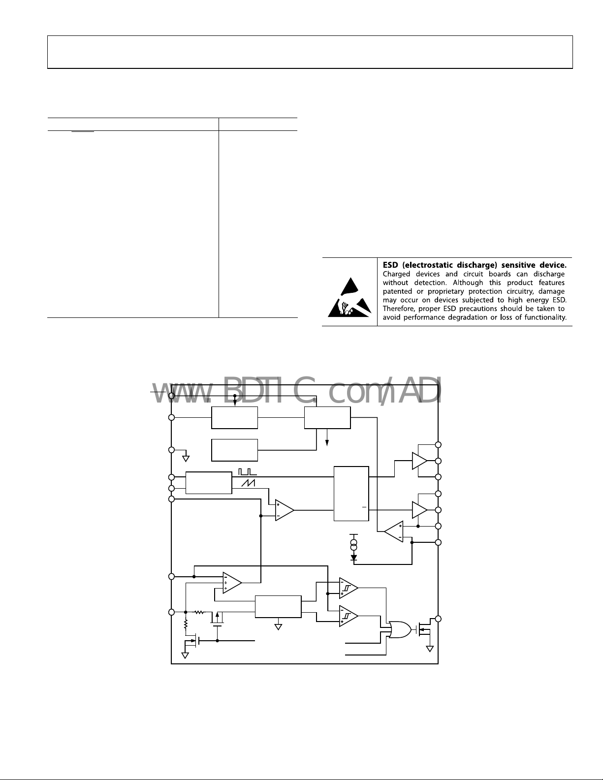
SIMPLIFIED BLOCK DIAGRAM
SHDN
VCC
GND
FREQ
SYNC
OMP
FB
SS
SHUTDOWN
OSCILLAT OR
100kΩ
2.5kΩ
THERMAL
FAULT
LOGICUVLO
FAULT
S
PWM
R
VCC
OV0.6V
REFERENCE
UV0.8V
UVLO
THSD
Figure 3. Simplified Block Diagram
ADP1821
BST
DH
Q
Q
SW
PVCC
DL
PGND
CSL
PWGD
05310-003
Rev. C | Page 5 of 24
Page 6
ADP1821
www.BDTIC.com/ADI
PIN CONFIGURATION AND FUNCTION DESCRIPTIONS
1
BST
2
DH
3
SW
ADP1821
TOP VIEW
4
SYNC
FREQ
SHDN
PWGD
GND SS
(Not to Scale)
5
6
7
8
Figure 4. Pin Configuration
16
PVCC
15
DL
14
PGND
13
CSL
12
VCC
11
COMP
10
FB
9
05310-004
Table 3. Pin Function Descriptions
Pin No. Mnemonic Description
1 BST
High-Side Gate Driver Boost Capacitor Input. A capacitor between SW and BST powers the high-side gate driver, DH.
The capacit
or is charged through a diode from PVCC when the low-side MOSFET is on. Connect a 0.1 µF or greater
ceramic capacitor from BST to SW and a Schottky diode from PVCC to BST to power the high-side gate driver.
2 DH
3 SW
4 SYNC
High-Side Gate Driver Output. Connect DH to the gate of the ex
powered from the capacitor between SW and BST, and its voltage swings between V
Power Switch Node. Connect the source of the high-side, N-channel MOSFET switch and the drain of the low-side,
channel MOSFET synchronous rectifier to SW. SW powers the output through the output LC filter.
NFrequency Synchronization Input. Drive SYNC with an external 300 kHz to 1.2 MHz signal to synchronize the converter
switching fr
equency to the applied signal. The maximum SYNC frequency is limited to 2 times the nominal internal
ternal high-side, N-channel MOSFET switch. DH is
SW
and V
BST
.
frequency selected by FREQ. Do not leave SYNC unconnected; when not used, connect SYNC to GND.
5 FREQ
6
SHDN
Frequency Select Input. FREQ selects the converter switching frequency. Drive FREQ low to select 300 kHz, or high
t 600 kHz. Do not leave FREQ unconnected.
to selec
Active Low, DC-to-DC Shutdown Input. Drive SHDN high to turn on the converter and low to turn it off. Connect
SHDN to VCC for automatic startup.
7 PWGD
Open-Drain, Power-Good Output. PWGD sinks current to GND
when the output voltage is above or below the
regulation voltage. Connect a pull-up resistor from PWGD to VDD for a logical power-good indicator.
8 GND Analog Ground. Connect GND to PGND at a single point as close as possible to the internal circuitry (IC).
9 SS
Soft Start Control Input. A capacitor from SS to GND controls the soft start period. When the output is overloaded,
SS is dischar
ged to prevent excessive input current while the output recovers. Connect a 1 nF capacitor to a 1 µF
capacitor from SS to GND to set the soft start period. See the Soft Start section.
10 FB
Voltage Feedback Input. Connect to a resistive voltage divider from the output to FB to set the output v
the Setting the Output Voltage section.
11 COMP
12 VCC
Compensation Node. Connect a resistor-capacitor network from COMP to FB to compensate the regulation control
system. S
Internal Power Supply Input. VCC powers the in
ee the Compensation section.
ternal circuitry. Bypass VCC to GND with a 0.1 µF or greater
capacitor connected as close as possible to the IC.
13 CSL
Low-Side Current Sense Input. Connect CSL to SW thr
urrent Limit section.
C
ough a resistor to set the current limit. See the Setting the
14 PGND Power Ground. Connect GND to PGND at a single point as close as possible to the IC.
15 DL
Low-Side Gate Driver Output. Connect DL to the gate of the low
-side, N-channel MOSFET synchronous rectifier. The
DL voltage swings between PGND and PVCC.
16 PVCC
Internal Gate Driver Power Supply Input. PVCC powers the low-side gate driver, DL. Bypass PVCC to PGND with a
1 µF or gr
eater capacitor connected as close as possible to the IC.
oltage. See
Rev. C | Page 6 of 24
Page 7
ADP1821
www.BDTIC.com/ADI
TYPICAL PERFORMANCE CHARACTERISTICS
97
96
95
94
93
92
91
EFFICIENCY (%)
90
89
88
87
0
3.3V OUTPUT
1.8V OUTPUT
2 4 6 8 10 12 14
LOAD CURRENT (A)
TA = 25°C
FREQUENCY = 300kHz
16
05310-005
0.6003
0.6002
0.6001
0.6000
0.5999
0.5998
FEEDBACK VOLT AGE (V)
0.5997
0.5996
–50
–30 –10 10 30 50 70 90
TEMPERATURE (° C)
110
05310-008
Figure 5. Efficiency vs. Load Current, V
94
TA = 25°C
FREQUENCY = 300kHz
92
90
88
86
EFFICIENCY (%)
84
82
80
0
2 4 6 8 10 12 14
3.3V OUTPUT
1.8V OUTPUT
LOAD CURRENT (A)
Figure 6. Efficiency vs. Load Current, V
1400
1200
1000
= 5 V, V
IN
= 12 V, V
IN
= 3.3 V, 1.8 V
OUT
= 3.3 V, 1.8 V
OUT
Figure 8. FB Regulation Voltage vs. Temperature
700
600
500
400
300
200
SWITCHING FREQUENCY ( kHz)
100
0
16
05310-006
–50
600kHz
300kHz
050
TEMPERATURE (° C)
100
05310-009
Figure 9. Switching Frequency vs. Temperature
OUTPUT VOLTAGE
(20mV/DIV)
800
600
VCC CURRENT (µA)
400
200
0
0
12345
VCC VOLTAG E (V)
6
05310-007
Figure 7. VCC Supply Current vs. VCC Voltage
Rev. C | Page 7 of 24
LOAD CURRENT
(5A/DIV)
Figure 10. Load Transient Response, 1.5 A to 15 A
5310-010
Page 8

ADP1821
www.BDTIC.com/ADI
OUTPUT VOLTAGE
OUTPUT VOLTAGE
(50mV/DIV)
(1V/DIV)
SHDN (5V/DIV)
INPUT VOLTAGE
(5V/DIV)
Figure 11. Line Transient Response, 10 V to 16 V
OUTPUT VO LTAGE
(1V/DIV)
SHDN (5V/DIV)
PWGD (5V/DIV)
Figure 12. Power-On Response
PWGD (5V/DIV)
5310-011
5310-013
Figure 13. Power-On Response, Prebiased Output
OUTPUT VOL TAGE
(1V/DIV)
LOAD CURRENT
(10A/DIV)
5310-012
Figure 14. Output Short-Circui
t Response and Recovery
5310-014
Rev. C | Page 8 of 24
Page 9

ADP1821
www.BDTIC.com/ADI
THEORY OF OPERATION
The ADP1821 is a versatile, economical, synchronous-rectified,
fixed-frequency, PWM, voltage mode step-down controller
capable of generating an output voltage as low as 0.6 V. It is ideal
for a wide range of high power applications, such as DSP power
and processor core power in telecommunications, medical
imaging, and industrial applications. The ADP1821 controller
operates from a 3.7 V to 5.5 V supply with a power input voltage
ranging from 1.0 V to 24 V.
The ADP1821 operates at a fixed, internally set 300 kHz or
600
kHz switching frequency that is controlled by the state of
the FREQ input. The high frequency reduces external component size and cost while maintaining high efficiency. For noise
sensitive applications where the switching frequency needs to be
more tightly controlled, synchronize the ADP1821 to an external
signal whose frequency is between 300 kHz and 1.2 MHz.
The ADP1821 includes adjustable soft start with output reverse-
urrent protection, and a unique adjustable, lossless current
c
limit. It operates over the −40°C to +125°C temperature range
and is available in a space-saving, 16-lead QSOP.
SOFT START
When powering up or resuming operation after shutdown, overload, or short-circuit conditions, the ADP1821 employs an
adjustable soft start feature that reduces input current transients
and prevents output voltage overshoot at start-up and overload
conditions. The soft start period is set by the value of the soft
start capacitor, C
When starting the ADP1821, C
enabled when
lockout threshold. C
internal 100 k resistor. As C
FB is limited to the lesser of either the voltage at SS or the internal
0.6 V reference voltage. As the voltage at SS rises, the output
voltage rises proportionally until the voltage at SS exceeds 0.6 V. At
this time, the output voltage is regulated to the desired voltage.
If the output voltage is precharged prior to turn-on, the ADP1821
imits reverse inductor current, which would discharge the output
l
voltage. Once the voltage at SS exceeds the 0.6 V regulation voltage,
the reverse current is re-enabled to allow the output voltage
regulation to be independent of load current.
, between SS and GND.
SS
is initially discharged. It is
SS
SHDN
is high and VCC is above the undervoltage
begins charging to 0.8 V through an
SS
charges, the regulation voltage at
SS
ERROR AMPLIFIER
The ADP1821 error amplifier is an operational amplifier. The
ADP1821 senses the output voltages through an external
resistor divider at the FB pin. The FB pin is the inverting input
to the error amplifier. The error amplifier compares this feedback voltage to the internal 0.6 V reference, and the output of
the error amplifier appears at the COMP pin. The COMP pin
voltage then directly controls the duty cycle of the switching
converter.
A series/parallel RC network is tied between the FB pin and the
OMP pin to provide the compensation for the buck converter
C
Rev. C | Page 9 of 24
control loop. A detailed design procedure for compensating the
system is provided in the
lator section.
Regu
The error amplifier output is clamped between a lower limit of
ab
out 0.7 V and a higher limit of about 2.4 V. When the COMP pin
is low, the switching duty cycle goes to 0%, and when the COMP
pin is high, the switching duty cycle goes to the maximum.
The SS pin is an auxiliary positive input to the error amplifier.
hichever voltage is lowest, SS or the internal 0.6 V reference,
W
controls the FB pin voltage and thus the output. As a consequence, if two of these inputs are close to each other, a small
offset is imposed on the error amplifier.
Compensating the Voltage Mode Buck
CURRENT-LIMIT SCHEME
The ADP1821 employs a unique, programmable, cycle-by-cycle,
lossless current-limit circuit that uses an ordinary, inexpensive
resistor to set the threshold. Every switching cycle, the synchronous
rectifier turns on for a minimum time and the voltage drop across
the MOSFET R
too high.
This measurement is done by an internal current limit comparator
is connected between the switch node (that is the drain of the
rectifier MOSFET) and the CSL pin. The CSL pin, which is the
inverting input of the comparator, forces 50 A through the
resistor to create an offset voltage drop across it.
When the inductor current is flowing in the MOSFET rectifier,
i
R
current-limit set resistor, the inverting comparator input is
similarly forced below PGND and an overcurrent fault is flagged.
The normal transient ringing on the switch node is ignored
for 100 n
the over current condition must also persist for 100 ns for a
fault to be flagged.
When the ADP1821 senses an overcurrent condition, the next
s
through an internal 2.5 k resistor, and the error amplifier
output voltage is pulled down. The output behaves like a
constant current source around the preset current limit when
the overcurrent condition exists. The ADP1821 remains in this
mode for as long as the overcurrent condition persists. In the
event of a short circuit, the short-circuit output current is the
current limit set by the R
cycle. When the overcurrent condition is removed, operation
resumes in soft start mode.
The ADP1821 also offers a technique for implementing a
c
use of an additional resistor. See the Setting the Current Limit
s
and an external current-limit set resistor. The resistor
ts drain is forced below PGND by the voltage drop across its
. If the R
DSON
s after the synchronous rectifier turns on, therefore,
witching cycle is suppressed, the soft start capacitor is discharged
urrent-limit foldback in the event of a short circuit with the
ection for more information.
is measured to determine if the current is
DSON
voltage drop exceeds the preset drop on the
DSON
resistor and is monitored cycle by
CL
Page 10

ADP1821
www.BDTIC.com/ADI
MOSFET DRIVERS
The DH pin drives the high-side switch MOSFET. This is a
boosted 5 V gate driver that is powered by a bootstrap capacitor
circuit. This configuration allows the high-side, N-channel
MOSFET gate to be driven above the input voltage, allowing full
enhancement and a low voltage drop across the MOSFET. The
bootstrap capacitor is connected from the SW pin to the BST
pin. A bootstrap Schottky diode connected from the PVCC pin
to the BST pin recharges the bootstrap capacitor every time the
SW node goes low. Use a bootstrap capacitor value greater than
100× the high-side MOSFET input capacitance.
In practice, the switch node can run up to 24 V of input voltage,
he boost nodes can operate more than 5 V above this to
and t
allow full gate drive. The power input voltage can be run from
1 V to 24 V.
The switching cycle is initiated by the internal clock signal. The
hig
h-side MOSFET is turned on by the DH driver, and the SW
node goes high, pulling up on the inductor. When the internally
generated ramp signal crosses the COMP pin voltage, the switch
MOSFET is turned off and the low-side synchronous rectifier
MOSFET is turned on by the DL driver. Active break-beforemake circuitry as well as a supplemental fixed dead time are
used to prevent cross-conduction in the switches.
The DL pin provides the gate drive for the low-side MOSFET
syn
chronous rectifier. Internal circuitry monitors the external
MOSFETs to ensure break-before-make switching to prevent
cross-conduction. An active dead-time reduction circuit
reduces the break-before-make time of the switching to limit
the losses due to current flowing through the synchronous
rectifier body diode.
The PVCC pin provides power to the low-side drivers. It is
ted to 5.5 V maximum input and should have a local
limi
decoupling capacitor to PGND.
The synchronous rectifier is turned on for a minimum time
o
f about 200 ns on every switching cycle in order to sense the
current. This and the nonoverlap dead time put a limit on the
maximum high-side switch duty cycle based on the selected
switching frequency. Typically, this is about 90% at 300 kHz
switching, and at 1 MHz switching, it reduces to about 70%
maximum duty cycle.
INPUT VOLTAGE RANGE
The ADP1821 takes its internal power from the VCC and PVCC
inputs. PVCC powers the low-side MOSFET gate drive (DL),
and VCC powers the internal control circuitry. Both of these
inputs are limited to between 3.7 V and 5.5 V. Bypass PVCC to
PGND with a 1 µF or greater capacitor. Bypass VCC to GND
with a 0.1 µF or greater capacitor.
The power input to the dc-to-dc converter can range between
1.2× th
e output voltage and 24 V. Bypass the power input to
PGND with a suitably large capacitor. See the Selecting the
Inp
ut Capacitor section.
SETTING THE OUTPUT VOLTAGE
The output voltage is set using a resistive voltage divider from
the output to FB. The voltage divider drops the output voltage
to the 0.6 V FB regulation voltage to set the regulation output
voltage. The output voltage is set to voltages as low as 0.6 V and
as high as 85% of the minimum power input voltage (see the
Feedback Voltage Divider section).
SWITCHING FREQUENCY CONTROL AND SYNCHRONIZATION
The ADP1821 has a logic-controlled frequency select input (FREQ)
which sets the switching frequency to 300 kHz or 600 kHz. Drive
FREQ low for 300 kHz and high for 600 kHz.
The SYNC input is used to synchronize the converter switching
requency to an external signal. The converter switching can be
f
synchronized to an external signal. This allows multiple ADP1821
converters to be operated at the same frequency to prevent
frequency beating or other interactions.
To synchronize the ADP1821 switching to an external signal,
rive the SYNC input with a synchronizing signal. The ADP1821
d
can only synchronize up to 2× the nominal oscillator frequency.
If the frequency is set to 300 kHz (FREQ connected to GND),
then the synchronization frequency needs to be in between
300 kHz and 600 kHz. Since the 300 kHz setting has a minimum specification (see
o
f 375 kHz over the specified temperature range, the recommended synchronization frequency range is between 375 kHz
and 500 kHz to cover the whole range of part-to-part variation
and over the operating temperature range. If the frequency is set
to 600 kHz (FREQ connected to VCC), then the synchronization
frequency needs to be in between 600 kHz and 1.2 MHz. Since
the 600 kHz setting has a minimum specification (see
f 470 kHz and a maximum of 720 kHz over the specified tem-
o
perature range, the recommended synchronization frequency
range is between 720 kHz and 940 kHz to cover the whole range
of part-to-part variation and over the operating temperature
range. Driving SYNC faster than recommended for the FREQ
setting results in a small ramp signal, which could affect the
signal-to-noise ratio and the modulator gain and stability.
When an external clock is detected at the first SYNC edge,
t
he internal oscillator is reset and clock control shifts to SYNC.
The SYNC edges then trigger subsequent clocking of the PWM
outputs. The DH rising edges appear about 320 ns after the corresponding SYNC edge, and the frequency is locked to the
external signal. If the external SYNC signal disappears during
operation, the ADP1821 reverts to its internal oscillator and
experiences a delay of no more than a single cycle of the
internal oscillator.
Tabl e 1 ) of 250 kHz and a maximum
Tabl e 1 )
Rev. C | Page 10 of 24
Page 11

ADP1821
www.BDTIC.com/ADI
COMPENSATION
The control loop is compensated by an external series RC
network from COMP to FB and sometimes requires a series
RC in parallel with the top voltage divider resistor. COMP is
the output of the internal error amplifier.
The internal error amplifier compares the voltage at FB to the
in
ternal 0.6 V reference voltage. The difference between the two
(the feedback voltage error) is amplified by the error amplifier.
To optimize the ADP1821 for stability and transient response
for a given set of external components and input/output voltage
conditions, choose the compensation components carefully. For
more information on choosing the compensation components,
see the
Compensating the Voltage Mode Buck Regulator section.
POWER-GOOD INDICATOR
The ADP1821 features an open-drain, power-good output
(PWGD) that sinks current when the output voltage drops 8.3%
below or 25% above the nominal regulation voltage. Two comparators measure the voltage at FB to set these thresholds. The
PWGD comparator directly monitors FB, and the threshold is
fixed at 0.55 V for undervoltage and 0.75 V for overvoltage. The
PWGD output also sinks current if an overtemperature or input
undervoltage condition is detected and is operational with VCC
voltage as low as 1 V.
Use this output as a logical power-good signal by connecting a
pu
ll-up resistor from PWGD to an appropriate supply voltage.
THERMAL SHUTDOWN
The ADP1821 controller does not generate much heat under
normal conditions, even when driving a relatively large MOSFET.
However, the surrounding power components or other circuits
on the same PCB could heat up the PCB to an unsafe operating
temperature. The ADP1821 controller goes into shutdown and
shuts off the gate drivers when its junction temperature reaches
about 145°C. When the junction temperature drops below
about 135°C, the ADP1821 resumes normal operation in a soft
start mode.
SHUTDOWN CONTROL
The ADP1821 dc-to-dc converter features a low power shutdown mode that reduces quiescent supply current to 1 A. To
shut down the ADP1821, drive
SHDN
high. For automatic startup, connect
SHDN
low. To turn it on, drive
SHDN
to VCC.
Rev. C | Page 11 of 24
Page 12

ADP1821
Δ≅Δ
www.BDTIC.com/ADI
APPLICATION INFORMATION
SELECTING THE INPUT CAPACITOR
The input current to a buck converter is a pulsed waveform. It is
zero when the high-side switch is off and approximately equal
to the load current when it is on. The input capacitor carries the
input ripple current, allowing the input power source to supply
only the dc current. The input capacitor needs sufficient ripple
current rating to handle the input ripple and the equivalent series
resistance (ESR) that is low enough to mitigate input voltage
ripple. For the usual current ranges for these converters, good
practice is to use two parallel capacitors placed close to the drains
of the high-side switch MOSFETs, one bulk capacitor of sufficiently high current rating as calculated in Equation 1, along
with 10 F of ceramic capacitor.
Select an input bulk capacitor based on its ripple current rating.
irst, determine the duty cycle of the output with the larger load
F
current by
V
OUT
D =
(1)
V
IN
Second, determine the input capacitor ripple current, which is
pproximately
a
II
LRIPPLE
(2)
()
DD
−≈1
where:
I
is the maximum inductor or load current for the channel.
L
D is the duty cycle.
Use this method to determine the input capacitor ripple current
ra
ting for duty cycles between 20% and 80%.
For duty cycles less than 20% or greater than 80%, use an input
c
apacitor with a ripple current rating of
I
RIPPLE
> 0.4 I
L
(3)
OUTPUT LC FILTER
The output LC filter smoothes the switched voltage at SW,
making the output voltage an almost dc voltage. Choose the
output LC filter to achieve the desired output ripple voltage.
Because the output LC filter is part of the regulator negativefeedback control loop, the choice of the output LC filter
components affects the regulation control loop stability.
Choose an inductor value such that the inductor ripple current
pproximately 1/3 of the maximum dc output load current.
is a
Using a larger value inductor results in a physical size larger
than required and using a smaller value results in increased
losses in the inductor and/or MOSFET switches.
Use the following equation to choose the inductor value:
1
=
L 1
SW
V
OUT
Δ×
If
L
⎡
⎢
⎣
⎤
V
OUT
−
(4)
⎥
V
IN
⎦
where:
L
is the inductor value.
f
is the switching frequency.
SW
V
is the output voltage.
OUT
is the input voltage.
V
IN
ΔI
is the inductor ripple current, typically 1/3 of the maximum
L
dc load current.
Choose the output bulk capacitor to set the desired output voltage
r
ipple. The impedance of the output capacitor at the switching
frequency multiplied by the ripple current gives the output
voltage ripple. The impedance is made up of the capacitive
impedance plus the nonideal parasitic characteristics, the ESR
and the equivalent series inductance (ESL). The output voltage
ripple can be approximated with
2
OUT
L
⎜
8
⎝
⎛
2
⎜
ESRIV
+Δ=Δ
⎞
1
⎟
+
⎟
Cf
SW
OUT
⎠
2
(5)
)4(
ESLf
SW
where:
is the output ripple voltage.
ΔV
OUT
ΔI
is the inductor ripple current.
L
ESR is t
he equivalent series resistance of the output capacitor
(or the parallel combination of ESR of all output capacitors).
ESL is t
he equivalent series inductance of the output capacitor
(or the parallel combination of ESL of all capacitors).
Note that the factors of 8 and 4 in Equation 5 would normally
b
e 2π for sinusoidal waveforms, but the ripple current waveform in this application is triangular. Parallel combinations
of different types of capacitors, for example, a large aluminum
electrolytic in parallel with MLCCs, may give different results.
Usually the impedance is dominated by ESR at the switching
requency so this equation reduces to
f
ESRIV
(6)
OUT
L
Electrolytic capacitors have significant ESL also, on the order
of 5 nH to 20 nH, depending on type, size, and geometry; and
PCB traces contribute some ESR and ESL as well. However,
using the maximum ESR rating from a capacitor data sheet
usually provides some margin such that measuring the ESL is
not usually required.
Rev. C | Page 12 of 24
Page 13

ADP1821
(
)
PPP
P
++≅
www.BDTIC.com/ADI
In the case of output capacitors where the impedance of the
ESR and ESL are small at the switching frequency, for instance,
where the output capacitor is a bank of parallel MLCC capacitors, the capacitive impedance dominates and the ripple
equation reduces to
V
OUT
8
(7)
fC
SW
OUT
Δ
I
L
≅Δ
Make sure that the ripple current rating of the output capacitors
i
s greater than the maximum inductor ripple current.
During a load step transient on the output, the output capacitor
s
upplies the load until the control loop has a chance to ramp the
inductor current. This initial output voltage deviation due to a
change in load is dependent on the output capacitor characteristics. Again, usually the capacitor ESR dominates this response,
and the V
current value for I
in Equation 6 can be used with the load step
OUT
.
L
SELECTING THE MOSFETS
The choice of MOSFET directly affects the dc-to-dc converter
performance. The MOSFET must have low on resistance to reduce
2
I
R losses and low gate charge to reduce transition losses. In
addition, the MOSFET must have low thermal resistance to
ensure that the power dissipated in the MOSFET does not result
in excessive MOSFET die temperature.
The high-side MOSFET carries the load current during on time
a
nd carries all the transition losses of the converter. Typically,
the lower the MOSFET on resistance, the higher the gate charge
and vice versa. Therefore, it is important to choose a high-side
MOSFET that balances the two losses. The conduction loss of
the high-side MOSFET is determined by the equation
⎞
⎛
2
()
≅
where:
P
is the conduction power loss.
C
is the MOSFET on resistance.
R
DSON
The gate charging loss is approximated by the equation
where:
P
is the gate charging loss power.
G
is the gate driver supply voltage.
V
PVCC
Q
is the MOSFET total gate charge.
G
is the converter switching frequency.
f
SW
The high-side MOSFET transition loss is approximated by the
eq
uation
IN
P+=
T
LOAD
where:
P
is the high-side MOSFET switching loss power.
T
is the MOSFET rise time.
t
R
t
is the MOSFET fall time.
F
V
OUT
⎟
⎜
RIP
DSONLOADC
⎜
⎝
fQVP ≅
(9)
SWGPVCCG
2
(8)
⎟
V
IN
⎠
fttIV
FR
SW
(10)
Rev. C | Page 13 of 24
The total power dissipation of the high-side MOSFET is the
s
um of all the previous losses, or
(11)
GC
T
where P
D
is the total high-side MOSFET power loss.
D
The conduction losses may need an adjustment to account
fo
r the MOSFET R
MOSFET R
DSON
data sheet should list the thermal resistance of the package, θ
variation with temperature. Note that
DSON
increases with increasing temperature. A MOSFET
JA
along with a normalized curve of the temperature coefficient of
the R
. For the power dissipation estimated above, calculate
DSON
the MOSFET junction temperature rise over the ambient
temperature of interest.
T
= TA + θJAPD (12)
J
Then calculate the new R
curve and the R
spec at 25°C. A typical value of the temperature
DSON
coefficient (TC) of the R
method to calculate the MOSFET R
temperature, T
R
DSON
, is
J
@ TJ = R
DSON
from the temperature coefficient
DSON
is 0.004/°C, thus, an alternate
DSON
at a second
DSON
@ 25°C(1 + TC(TJ − 25°C)) (13)
Next, the conduction losses can be recalculated and the proce
dure iterated once or twice until the junction temperature
calculations are relatively consistent.
The synchronous rectifier, or low-side MOSFET, carries the
uctor current when the high-side MOSFET is off. The low-
ind
side MOSFET transition loss is small and can be neglected in
the calculation. For high input voltage and low output voltage,
the low-side MOSFET carries the current most of the time.
Therefore, to achieve high efficiency, it is critical to optimize
the low-side MOSFET for low on resistance. In cases where the
power loss exceeds the MOSFET rating or lower resistance is
required than is available in a single MOSFET, connect multiple
low-side MOSFETs in parallel. The equation for low-side
MOSFET power loss is
()
RIP 1
DSONLOADLS
⎢
⎣
⎡
2
⎤
V
OUT
−≅
(14)
⎥
V
IN
⎦
where:
P
is the low-side MOSFET on resistance.
LS
R
is the total on resistance of the low-side MOSFET(s).
DSON
Check the gate charge losses of the synchronous rectifier
usin
equation (Equation 9) to be sure it is reasonable.
g the P
G
If multiple low-side MOSFETs are used in parallel, then use
the parallel combination of the on resistances for determining
R
to solve this equation.
DSON
,
Page 14

ADP1821
V
www.BDTIC.com/ADI
SETTING THE CURRENT LIMIT
The current-limit comparator measures the voltage across the
low-side MOSFET to determine the load current.
The current limit is set through the current-limit resistor, R
CSL, the current sense pin, sources 50 A through R
creates an offset voltage of R
multiplied by the 50 A CSL
CL
CL
current. When the drop across the low-side MOSFET R
equal to or greater than this offset voltage, the ADP1821 flags
a current-limit event.
Because the CSL current and the MOSFET R
vary over process
DSON
and temperature, the minimum current limit should be set to
ensure that the system can handle the maximum desired load
current. To do this, use the peak current in the inductor, which
is the desired current-limit level plus the ripple current, the
maximum R
of the MOSFET at its highest expected tem-
DSON
perature, and the minimum CSL current.
R =
where I
CL
LPK
DSON
is the peak inductor current.
)( MAX
A42
(15)
RI
LPK
When an overcurrent event occurs, the overcurrent comparator
prevents switching cycles until the rectifier current has decayed
below the threshold. The overcurrent comparator is blanked for
the first 100 ns of the synchronous rectifier cycle to prevent
switch node ringing from falsely tripping the current limit.
ADP1821 senses the current limit during the off cycle. When
the current-limit condition occurs, the output behaves like a
constant current source around the preset current limit. When
the overload condition is removed, the output recovers with the
normal soft start slope and does not overshoot.
In the event of a short circuit, the ADP1821 offers a technique
for implementing a current-limit foldback with the use of an
additional resistor, as shown in Figure 15. Resistor R
LO
responsible for setting the foldback current limit during a short
circuit, and Resistor R
normal current limit. R
is mainly responsible for setting up the
HI
is lower than RHI. These current-limit
LO
sense resistors can be calculated as
RI
MAXDSONPKFOLDBACK
)(
=
R
LO
R
=
HI
I
LPK
A
μ
42
V
OUT
R
MAXDSON
R
LO
(16)
(17)
A
μ
42)(−
where:
I
PKFOLDBACK
I
LPK
is the desired short circuit peak inductor current limit.
is the peak inductor current limit during normal operation
and is also used in Equation 15.
.
CL
. This
is
DSON
The
is largely
IN
ADP1821
DH
DL
CSL
Figure 15. Short-Circuit Current Foldback Scheme
M1
M2
L
R
R
LO
HI
V
OUT
C
OUT
05310-023
Because the buck converter is usually running at a fairly high
current, PCB layout and component placement may affect
the current-limit setting. An iteration of the R
or RLO and RHI
CL
values may be required for a particular board layout and MOSFET
selection. If alternate MOSFETs are substituted at some point in
production, these resistor values may also need an iteration.
FEEDBACK VOLTAGE DIVIDER
The output regulation voltage is set through the feedback voltage
divider. The output voltage is reduced through the voltage
divider and drives the FB feedback input. The regulation
threshold at FB is 0.6 V. The maximum input bias current into
FB is 100 nA. For a 0.15% degradation in regulation voltage and
with 100 nA bias current, the low-side resistor, R
, needs to be
BOT
less than 9 kΩ, which results in 67 µA of divider current. For
R
, use 1 k to 10 k. A larger value resistor can be used, but
BOT
results in a reduction in output voltage accuracy due to the
input bias current at the FB pin, whereas lower values cause
increased quiescent current consumption. Choose R
TOP
to set
the output voltage by using the following equation:
VVRR_
⎛
OUT
⎜
=
BOTTOP
⎜
V
⎝
⎞
FB
⎟
(18)
⎟
FB
⎠
where:
is the high-side voltage divider resistance.
R
TOP
is the low-side voltage divider resistance.
R
BOT
V
is the regulated output voltage.
OUT
is the feedback regulation threshold, 0.6 V.
V
FB
COMPENSATING THE VOLTAGE MODE BUCK REGULATOR
Assuming the LC filter design is complete, the feedback control system can be compensated. Good compensation is critical to proper
operation of the regulator. Calculate the quantities in Equation 19
through Equation 47 to derive the compensation values.
The goal is to guarantee that the voltage gain of the buck converter crosses unity at a slope that provides adequate phase margin
for stable operation. Additionally, at frequencies above the crossover frequency, f
attenuation of switching noise are important secondary goals.
, guaranteeing sufficient gain margin and
CO
Rev. C | Page 14 of 24
Page 15

ADP1821
www.BDTIC.com/ADI
For initial practical designs, a good choice for the crossover
frequency is 1/10 of the switching frequency; first calculate
f
SW
f =
CO
(19)
10
This gives sufficient frequency range to design a compensation
hat attenuates switching artifacts, yet also gives sufficient
t
control loop bandwidth to provide good transient response.
The output LC filter is a resonant network that inflicts two poles
on the response at a Frequency f
up
f
1
=
LC
2
(20)
LCπ
, so next calculate
LC
The LC corner frequency is about two orders of magnitude
elow the switching frequency, and therefore about one order of
b
magnitude below crossover. To achieve sufficient phase margin
at crossover to guarantee stability, the design must compensate
for the two poles at the LC corner frequency with two zeros to
boost the system phase prior to crossover. The two zeros require
an additional pole or two above the crossover frequency to
guarantee adequate gain margin and attenuation of switching
noise at high frequencies.
Depending on component selection, one zero might already be
nerated by the ESR of the output capacitor. Calculate this zero
ge
f
ESR
, as
ESR
1
CRπ
OUT
corner frequency,
= (21)
f
ESR
2
This zero is often near or below crossover and is useful in
ringing back some of the phase lost at the LC corner.
b
Figure 16 shows a typical bode plot of the LC filter by itself.
The gain of the LC filter at crossover can be linearly
a
pproximated from Figure 16 as
AAA +=
FILTER
A logdB20logdB40
FILTER
If f
≈ fCO, then add another 3 dB to account for the local
ESR
ESRLC
⎛
⎞
f
ESR
⎜
×−=
⎟
⎜
⎟
f
LC
⎝
⎠
⎛
⎞
f
CO
⎜
⎟
×−
(22)
⎜
⎟
f
ESR
⎝
⎠
difference between the exact solution and the preceding linear
approximation.
To compensate the control loop, the gain of the system must be
rought back up so that it is 0 dB at the desired crossover
b
frequency. Some gain is provided by the PWM modulation
itself, and it is given by
=
A log20
MOD
⎛
⎜
⎜
⎝
V
⎞
V
IN
⎟
(23)
⎟
RAMP
⎠
For systems using the internal oscillator, this becomes
⎞
⎛
V
IN
⎟
A
MOD
⎜
=
log20
⎜
⎝
(24)
⎟
V25.1
⎠
LC FILTER BODE PLOT
GAIN
0dB
PHASE
0°
–90°
–180°
f
LCfESRfCO
–40dB/dec
–20dB/dec
Figure 16. LC Filter Bode Plot
A
Φ
FILTER
FILTER
f
SW
FREQUENCY
Note that if the converter is being synchronized, the ramp
voltage, V
, is lower than 1.25 V by the percentage of
RAMP
frequency increase over the nominal setting of the FREQ pin
⎛
⎞
f
FREQ
⎜
⎟
=
V V25.1
RAMP
⎜
⎝
(25)
⎟
f
SYNC
⎠
The rest of the system gain is needed to reach 0 dB at crossover.
T
he total gain of the system therefore, is given by
AT = A
MOD
+ A
FILTER
+ A
(26)
COMP
where:
A
is the gain of the PWM modulator.
MOD
A
is the gain of the LC filter including the effects of the
FILTER
ESR zero.
A
is the gain of the compensated error amplifier.
COMP
Additionally, the phase of the system must be brought back up
o guarantee stability. Note from the bode plot of the filter that
t
the LC contributes −180° of phase shift. Additionally, because
the error amplifier is an integrator at low frequency, it contributes an initial −90°. Therefore, before adding compensation or
accounting for the ESR zero, the system is already down −270°.
To avoid loop inversion at crossover, or −180° phase shift, a
good initial practical design is to require a phase margin of 60°,
which gives an overall phase loss of −120° from the initial low
frequency dc phase. The goal of the compensation is to boost
the phase back up from −270° to −120° at crossover.
05310-015
Rev. C | Page 15 of 24
Page 16

ADP1821
www.BDTIC.com/ADI
Two common compensation schemes are used, which are
sometimes referred to as Type II or Type III compensation,
depending on whether the compensation design includes two
or three poles. (Dominant pole compensations, or single pole
compensation, is referred to as Type I compensation, but it is
not very useful for dealing successfully with switching regulators.)
If the zero produced by the ESR of the output capacitor provides
s
ufficient phase boost at crossover, Type II compensation is
adequate. If the phase boost produced by the ESR of the output
capacitor is not sufficient, another zero is added to the compensation network, and thus Type III is used.
In Figure 17, the location of the ESR zero corner frequency gives
sig
nificantly different net phase at the crossover frequency.
LC FILTER BODE PLOT
PHASE CONTRIBUTI ON AT CROSSO VER
GAIN
PHASE
OF VARIOUS ESR ZERO CORNERS
f
f
0dB
0°
–90°
–180°
f
–40dB/dec
–20dB/dec
ESR2
ESR1
LC
ESR3
fCOf
Φ
1
Φ
Φ
f
SW
FREQUENCY
2
3
Figure 17. LC Filter Bode Plot
Use the following guidelines for selecting between Type II and
Type III compensators.
f
ESRZ
ESRZ
CO
, use Type II compensation.
2
f
CO
, use Type III compensation.
2
If
If
f ≤
f >
The following equations were used for the calculation of the
co
mpensation components as shown in Figure 18 and Figure 19:
1
f
1
Z
f+=
2
Z
=
2
(27)
CR
π
IZ
1
π
(28)
)(2
RRC
FFTOPFF
f+=
P
1
f
P
2
=
1
π
2
R
Z
1
CR
π
2
where:
f
is the zero produced in the Type II compensation.
Z1
f
is the zero produced in the Type III compensation.
Z2
f
is the pole produced in the Type II compensation.
P1
f
in the pole produced in the Type III compensation.
P2
Type II Compensator
G
(dB)
PHASE
–180°
–270°
R
OUT
TOP
R
BOT
FROM
V
Figure 18. Type II Compensation
If the output capacitor ESR zero frequency is sufficiently low (≤ ½
of the crossover frequency), use the ESR to stabilize the regulator.
In this case, use the circuit shown in Figure 18. Calculate the
mpensation resistor, Rz, with the following equation:
co
R =
Z
where:
05310-016
fCO is chosen to be 1/10 of f
V
is 1.25 V.
RAMP
Next, choose the compensation capacitor to set the compensation
f
, to the lesser of ¼ of the crossover frequency or ½ of the
o,
zer
Z1
LC resonant frequency
f
Z
1
ff
or
f
LC
f
Z
1
Solving for C
C
=
I
==
2
2
in Equation 32 yields
I
20
(34)
fR
π
SWZ
(29)
CC
HFI
CC
HFI
(30)
FFFF
–
1
S
L
O
P
E
f
Z
C
R
Z
EA
ffVR
COESRRAMPTOP
2
fV
LCIN
SW.
SWCO
===
π
2
404
1
(33)
CR
π
IZ
–
1
S
L
O
P
E
f
P
HF
C
I
COMP
VREF
TO PWM
VRAMP
0V
5310-017
(31)
1
(32)
CR
IZ
Rev. C | Page 16 of 24
Page 17

ADP1821
www.BDTIC.com/ADI
Solving for CI in Equation 33 yields
1
=
C
I
π
Use the larger value of C
(35)
fR
LCZ
from Equation 34 or Equation 35.
I
Because of the finite output current drive of the error amplifier,
needs to be less than 10 nF. If it is larger than 10 nF, choose a
C
I
larger R
Next, choose the high frequency pole
Since
Solving for C
and recalculate RZ and CI until CI is less than 10 nF.
TOP
f
to be ½ of fSW.
P1
1
(36)
ff
=
SWP
1
2
C
<< CI, Equation 29 is simplified to
HF
1
f
=
1
P
π
2
HF
C
=
HF
π
(37)
CR
HFZ
in Equation 36 and Equation 37 yields
1
(38)
Rf
ZSW
Type III Compensator
–
FROM
V
OUT
1
G
S
L
(dB)
–90°
PHASE
–270°
R
FF
R
TOP
R
BOT
O
P
E
f
R
C
Z
FF
Figure 19. Type III Compensation
E
P
LO
–
S
1
1
+
Z
C
HF
EA
VREF
S
L
O
P
E
f
P
C
I
COMP
TO PWM
VRAMP
0V
5310-018
If the output capacitor ESR zero frequency is greater than ½ of
the crossover frequency, use Type III compensator as shown in
Figure 19. Set the poles and zeros as follows:
1
(39)
fff
==
SWPP
21
2
ff
ff
ZZ
21
SWCO
404
1
====
2
(40)
CR
π
IZ
or
1
2
f
LC
ff
2
ZZ
1
===
2
(41)
CR
π
IZ
Use the lower zero frequency from Equation 40 or Equation 41.
alculate the compensator resistor, R
C
ffVR
1
COZRAMPTOP
R =
Z
fV
LCIN
(42)
2
, by
Z
Next calculate C
C
=
I
Because of the finite output current drive of the error amplifier,
needs to be less than 10 nF. If it is larger than 10 nF, choose a
C
I
larger R
TOP
Since
C
<< CI, combining Equation 29 and Equation 39 yields
HF
C
HF
Next calculate the feedforward capacitor C
then Equation 28 is simplified to
f
=
Z
2
Solving
where
C
FF
C
FF
f
is obtained from Equation 40 or Equation 41.
Z2
The feedforward resistor,
Equation 30 and Equation 39
R
FF
Check that the calculated component values are reasonable.
or instance, capacitors smaller than about 10 pF should be
F
avoided. In addition, the ADP1821 error amplifier has finite
output current drive, so R
greater than 10 nF should be avoided. If necessary, recalculate
the compensation network with a different starting value of R
is too small, start with a smaller value of R
C
HF
small and C
In general, aluminum electrolytic capacitors have high ESR,
erefore, a Type II compensation is adequate. However, if
th
several aluminum electrolytic capacitors are connected in
parallel, producing a low effective ESR, then Type III compensation
is needed. In addition, ceramic capacitors have very low ESR, on
the order of a few milliohms, requiring Type III compensation for
ceramic output capacitors. Type III compensation offers better
performance than Type II in terms of more low frequency gain,
more phase margin, and less high frequency gain at the
crossover frequency.
I
1
(43)
2
fR
π
1
ZZ
and recalculate RZ and CI until CI is less than 10 nF.
1
=
π
2
(44)
Rf
ZSW
Assume RFF << R
FF.
1
(45)
RC
π
TOPFF
in Equation 45 yields
1
=
2
π
=
π
is too big, start with a larger value of R
I
(46)
fR
2
ZTOP
R
, can be calculated by combining
FF
1
(47)
fC
SWFF
values less than 3 kΩ and CI values
Z
TOP
. If RZ is too
TOP
.
TOP
TOP
,
. If
Rev. C | Page 17 of 24
Page 18

ADP1821
www.BDTIC.com/ADI
SETTING THE SOFT START PERIOD
The ADP1821 uses an adjustable soft start to limit the output
voltage ramp-up period, limiting the input inrush current. The
soft start is set by selecting the capacitor, C
The ADP1821 charges C
resistor. The voltage on C
⎛
CSS
R is the internal 100 k resistor.
where
⎜
⎜
⎝
to 0.8 V through an internal 100 kΩ
SS
while it is charging is
SS
t
⎞
RC
⎟
SS
−=
eV 1V8.0
(48)
⎟
⎠
, from SS to GND.
SS
The soft start period, t
, is achieved when V
SS
t
⎛
⎜
1V8.0V6.0
⎜
SS
Ω )(k100
C
SS
e
−=
⎝
⎞
⎟
(49)
⎟
⎠
or
t
SS
()
k100
C
SS
Solve for C
by
SS
C
= tSS × 7.21 µF/sec (51)
SS
⎛
⎜
1n1
⎜
⎝
⎞
V6.0
⎟
386.1
−−=
=
⎟
V8.0
⎠
= 0.6 V or
CSS
(50)
Rev. C | Page 18 of 24
Page 19

ADP1821
www.BDTIC.com/ADI
PCB LAYOUT GUIDELINE
In any switching converter, there are some circuit paths that
carry high dI/dt, which can create spikes and noise. Other
circuit paths are sensitive to noise and still others carry high
dc current and can produce significant IR voltage drops. The
key to proper PCB layout of a switching converter is to identify
these critical paths and arrange the components and copper
area accordingly. When designing PCB layouts, be sure to keep
high current loops small. In addition, keep compensation and
feedback components away from the switch nodes and their
associated components.
The following is a list of recommended layout practices for
AD
P1821, arranged in approximately decreasing order of
importance. A PCB layout example of the circuit shown in
Figure 23 is shown in Figure 20 and Figure 21.
• The current waveform in the top and bottom FETs is a pulse
with very high dI/dt, so the path to, through, and from each
individual FET should be as short as possible and the two
paths should be as similar as possible. In designs that use
a pair of D-Paks or SO-8 FETs on one side of the PCB, it is
best to counter-rotate the two so that the switch node is on
one side of the pair and the high side drain can be bypassed
to the low side source with a suitable ceramic bypass capacitor,
placed as close as possible to the FETs to minimize inductance
around this loop through the FETs and capacitor. The recommended bypass ceramic capacitor values range from 1 F to
22 F depending upon the output current. This bypass
capacitor is usually connected to a larger value bulk filter
capacitor and should be grounded to the PGND plane.
• GND, VCC bypass, soft start capacitor, and the bottom end
of the output feedback divider resistors should be tied to an
almost isolated, small AGND plane. All of these connections to
the AGND plane should be kept as short as possible.
high current or high dI/dt signals should be connected to
this AGND plane. The AGND area should be connected
through one wide trace to the negative terminal of the
output filter capacitors.
• The PGND pin handles high dI/dt gate drive current
returning from the source of the low side MOSFET. The
voltage at this pin also establishes the 0 V reference for the
overcurrent limit protection (OCP) function and the CSL
pin. A small PGND plane should connect the PGND pin
and the PVCC bypass capacitor through a wide and direct
path to the source of the low side MOSFET. The placement
is critical for controlling ground bounce. The negative
of C
IN
terminal of C
the low-side MOSFET.
needs to be placed very close to the source of
IN
No
• Avoid long traces or large copper areas at the FB and CSL
pins, which are low signal level inputs that are sensitive to
capacitive and inductive noise pickup. It is best to position
any series resistors and capacitors as closely as possible to
these pins. Avoid running these traces close and parallel to
high dI/dt
• The switch node is the noisiest place in the switcher circuit
with large ac and dc voltage and current. This node should
be wide to minimize resistive voltage drop. But to minimize
the generation of capacitively coupled noise, the total area
should be small. Place the FETs and inductor close together
on a small copper plane in order to minimize series
resistance and keep the copper area small.
• Gate drive traces (DH and DL) handle high dI/dt and
tend to produce noise and ringing. They should be as
short and direct as possible. If possible, avoid using feedthrough vias in the gate drive traces. If vias are needed, it
is best to use two relatively large ones in parallel to reduce
the peak current density and the current in each via. If the
overall PCB layout is less than optimal, slowing down the
gate drive slightly can be very helpful to reduce noise and
ringing. It is occasionally helpful to place small value resistors
(such as 5 or 10 Ω) in series with the gate leads, mainly
DH traces to the high side FET gates. These can be populated with 0 resistors if resistance is not needed. Note that
the added gate resistance increases the switching rise and
fall times, and that also increases the switching power loss
in the MOSFET.
• The negative terminal of output filter capacitors should be
tied closely to the source of the low side FET. Doing this
helps to minimize voltage difference between GND and
PGND at the ADP1821.
• Generally, be sure that all traces are sized according to the
current being handled as well as their sensitivity in the
circuit. Standard PCB layout guidelines mainly address
heating effects of current in a copper conductor. Although
these are completely valid, they do not fully cover other
concerns, such as stray inductance or dc voltage drop. Any
dc voltage differential in connections between ADP1821
GND and the converter power output ground can cause a
significant output voltage error, as it affects converter output
voltage according to the ratio with the 600 mV feedback
reference. For example, a 6 mV offset between ground on
the ADP1821 and the converter power output causes a 1%
error in the converter output voltage.
traces.
Rev. C | Page 19 of 24
Page 20

ADP1821
www.BDTIC.com/ADI
VIA TO 2 LAYER
SOME TRACES ARE OMITT ED FOR CLARI TY
Figure 20. Top Layer Layout Example of Circuit (See Figure 23)
AGND
05310-019
Figure 21. Bottom Layer Layout Example of Circuit (See Figure 23)
PGND
RECOMMENDED COMPONENT MANUFACTURERS
Table 4.
Vendor Components
AVX Corporation Capacitors
Central Semiconductor Corp. Diodes
Coilcraft®, Inc. Inductors
Diodes, Inc. Diodes
International Rectifier Diodes, MOSFETs
Murata Manufacturing Co., Ltd. Capacitors, inductors
ON Semiconductor® Diodes, MOSFETs
Rubycon Corporation Capacitors
Sanyo
Sumida Corporation Inductors
Taiyo Yuden, Inc. Capacitors, inductors
Toko America, Inc. Inductors
United Chemi-Con, Inc. Capacitors
Vishay Siliconix Diodes, MOSFETs, resistors, capacitors
Capacitors
05310-020
Rev. C | Page 20 of 24
Page 21

ADP1821
V
www.BDTIC.com/ADI
APPLICATION CIRCUITS
The ADP1821 controller can be configured to regulate an output
with a load of more than 20 A if the power components, such as
the inductor, MOSFETs, and the bulk capacitors are chosen
carefully to meet the power requirement. The maximum load
and power dissipation are limited by the power-train components. Figure 1 shows a typical application circuit that can drive
an output load of 20 A. Note that two low-side MOSFETs are
needed to deliver the 20 A load. In this example, two power rails
are needed: a 5 V bias supply, which needs to supply about 30
mA to power the ADP1821 at full load, and a power input rail,
which ranges from 2.5 V to 20 V. The bulk input and output
capacitors used in this example are Sanyo OSCON™ capacitors,
which have low ESR and high current ripple rating. An alternative
to the OSCON capacitors are the polymer aluminum capacitors
that are available from other manufacturers such as United
Chemi-Con. Aluminum electrolytic capacitors, such as the
1µF
10Ω
PVCC
6.65kΩ
1.5nF
VCC
ADP1821
SHDN
FREQ
SYNC
PWGD
COMP
SS
100nF
GND
AGND
BST
DH
SW
CSL
DL
PGND
FB
0.22µF
4.1kΩ
1µF
100kΩ
120pF
f
= 600kHz
SW
C
: MURATA, GRM21BR61A106K
IN2
C
: MURATA, G RM31CR60J107M
OUT3
M1, M2: VIS HAY, DUAL-CHANNEL MOSFET Si7940DP
Figure 22. Typical Application Circuit with all Multilayer Ceramic Capacitors (MLCC), 3.3 V to 5 V Input
D1
Rubycon ZLG low-ESR series, can also be paralleled up at the
input or output to meet the current ripple requirement. Because
the aluminum electrolytic capacitors have higher ESR and much
larger variation in capacitance over the operating temperature
range, a larger bulk input and output capacitance is needed to
reduce the effective ESR and suppress the current ripple.
The ADP1821 can be configured to drive an output load of
les
s than 1 A. Figure 22 shows a typical application circuit that
ives a 3 A load in an all multilayer ceramic capacitor (MLCC)
dr
solution. Notice that the two MOSFETs used in this example are
dual-channel MOSFETs in a PowerPAK® SO-8 package, which
reduces cost and saves layout space.
IN = 3.7V T O 5.5V
C
+
1µF
10V
M1
L1 = 2.2µH
M2
L1: TOKO , FDV0620-2R2M
C
OUT2
D1: VISHAY BAT54
C
IN1
: MURATA, G RM31CR60J476M
IN2
+
10µF
10V
×2
C
C
OUT2
47µF
6.3V
C
OUT3
100µF
6.3V
2kΩ
1kΩ
1µF
10V
OUT1
OUTPUT
1.8V, 3A
84.5Ω
8.2nF
5310-021
Rev. C | Page 21 of 24
Page 22

ADP1821
www.BDTIC.com/ADI
The ADP1821 can also be configured to run with an input voltage
higher than 5.5 V. Figure 23 shows a typical application circuit
hat operates from a 12 V input. An external LDO is built, with
t
an NPN, a 5.6 V Zener diode, and a resistor to step down the
Q1
V
BST
DH
SW
CSL
PGND
E
R4 3.3kΩ
DL
FB
C5
1µF
R7
10Ω
PVCC
VCC
C6
1µF
R6
100kΩ
R8
82kΩ
C2
18pF
C3
1nF
f
= 300kHz
SW
C
: SANYO, O SCON 20SP180M
IN2
C
: SANYO, O SCON 4SEPC680M
OUT2
D2: CENTRAL SEM I, CMOZ 5V6, 5.6V Z ENER
ADP1821
SHDN
FREQ
SYNC
PWGD
COMP
SS
C
SS
100nF
GND
AGND
Figure 23. Typical Application Circuit, 12 V Input
D1
C4
0.22µF
L1: COILTRONICS, HC7-2R2
Q1: CENTRAL S EMI, CMST 2222A, NPN
D1: CENTRAL SEMI , CMDSH2-4L
M1, M2: IRFR3709Z
input voltage from 12 V to 5 V to power the ADP1821. These
external signal components are cheap and small in size. Alternatively, LDOs such as the
T-23 package can be used for input voltages up to 12 V.
SO
D2
R5
1.2kΩ
M1
L1 = 2.2µH
M2
C
10µF
16V
C
IN1
+
180µF
20V
C
OUT1
10µF
6.3V
×2
INPUT
12V
IN2
+
C
OUT2
680µF
4V
×2
ADP3300 or the ADP3330 in a small
OUTPUT
1.8V, 10A
R3
2.7kΩ
C1
1.8nF
R1
20kΩ
R2
10kΩ
5310-022
Rev. C | Page 22 of 24
Page 23

ADP1821
www.BDTIC.com/ADI
OUTLINE DIMENSIONS
0.197
0.193
0.189
0.012
0.008
9
8
0.158
0.154
0.150
0.069
0.053
SEATING
PLANE
0.244
0.236
0.228
0.010
0.006
8°
0°
0.050
0.016
0.065
0.049
0.010
0.004
COPLANARITY
0.004
16
1
PIN 1
0.025
BSC
COMPLIANT TO JEDEC STANDARDS MO-137-AB
Figure 24. 16-Lead Shrink Small Outline Package [QSOP]
(RQ-16)
Dimensions shown in inches
ORDERING GUIDE
Model Temperature Range1 Package Description Package Option Quantity
ADP1821ARQZ-R72 –40°C to +85°C 16-Lead Shrink Small Outline Package [QSOP] RQ-16 1,000
ADP1821-EVAL Evaluation Board
1
Operating junction temperature is −40°C to +125°C.
2
Z = RoHS Compliant Part.
Rev. C | Page 23 of 24
Page 24

ADP1821
www.BDTIC.com/ADI
NOTES
©2005–2007 Analog Devices, Inc. All rights reserved. Trademarks and
registered trademarks are the property of their respective owners.
D05310-0-4/07(C)
Rev. C | Page 24 of 24
 Loading...