

Page 1
Dual LED Flash Driver with
http://www.BDTIC.com/ADI
FEATURES
Ultracompact solution
Small 2 mm × 1.5 mm 12-ball WLCSP package
Tiny, low profile 2.2 H power inductor
LED current source for local LED grounding and low EMI
Synchronous 2 MHz PWM boost convertor, no external diode
High efficiency: 88% peak
Reduces high levels of input battery current during flash
Limits battery current drain in torch mode
2
I
C programmable
Currents up to 400 mA in flash mode for two LEDs
Currents up to 500 mA in flash mode for one LED with
5% accuracy
Currents up to 160 mA in torch mode with 10% accuracy
Peak inductor current limit
Flash timer
Control
2
I
C-compatible control registers
External STROBE pin
External direct TORCH pin
TX_MASK input to prevent high input battery current levels
Safety
Thermal overload protection
Flash timeout
Inductor fault detection
Output overvoltage
Short circuit protection
Soft start reduces inrush input current
I2C-Compatible Interface
ADP1655
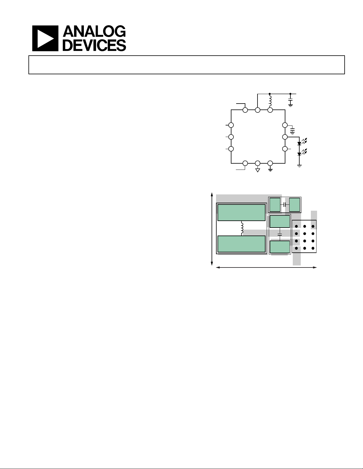
FUNCTIONAL BLOCK DIAGRAM
INPUT VOLTAGE = 2.5V TO 5.5V
2.2µH
STROBE VIN SW
TORCH
ADP1655
SCL/EN1
SDA/EN2
I2C/EN SGND PGND
VOUT
LED_OUT
TX_MASK
Figure 1.
Li-ION +
C1
L1
3mm
INDUCTOR
6.5mm
Figure 2. PCB Layout
10µF
10µF
8028-001
PGND
C2
LED
ANODE
Li-ION +
DIGITAL
INPUT/
OUTPUT
08028-002
APPLICATIONS
Camera-enabled cellular phones and smart phones
Digital still cameras, camcorders, and PDAs
GENERAL DESCRIPTION
The ADP1655 is a very compact, highly efficient, dual white
LED flash driver for high resolution camera phones, which
improves picture and video quality in low light environments.
The device integrates a 2 MHz synchronous inductive boost
convertor, an I
source. The high switching frequency enables the use of a tiny,
low profile 2.2 µH power inductor, and the current source
permits LED cathode grounding for thermally enhanced,
low EMI and compact layouts.
The efficiency is high over the entire battery voltage range to
maximize the input power to LED power conversion and
Rev. 0
Information furnished by Analog Devices is believed to be accurate and reliable. However, no
responsibility is assumed by Analog Devices for its use, nor for any infringements of patents or other
rights of third parties that may result from its use. Specifications subject to change without notice. No
license is granted by implication or otherwise under any patent or patent rights of Analog Devices.
Trademarks and registered trademarks are the property of their respective owners.
2
C-compatible interface and a 500 mA current
minimize battery current draw during flash events. In addition,
a Tx-mask input permits the flash LED current to reduce quickly
and, therefore, the battery current reduces quickly, during a
GSM power amplifier current burst.
2
The I
C-compatible interface enables the programmability
of timers, currents, and status bit readback for operation
monitoring and safety control.
The ADP1655 comes in a compact 12-ball 0.5 mm pitch
WLCSP package and is specified over the full −40°C to
+125°C junction temperature range.
One Technology Way, P.O. Box 9106, Norwood, MA 02062-9106, U.S.A.
Tel: 781.329.4700 www.analog.com
Fax: 781.461.3113 ©2009 Analog Devices, Inc. All rights reserved.
Page 2

ADP1655
http://www.BDTIC.com/ADI
TABLE OF CONTENTS
Features .............................................................................................. 1
Applications ....................................................................................... 1
Functional Block Diagram .............................................................. 1
General Description ......................................................................... 1
Revision History ............................................................................... 2
Specifications ..................................................................................... 3
Recommended Specifications: Input and Output Capacitance
and Inductance ............................................................................. 4
I2C-Compatible Interface Timing Specifications ..................... 5
Absolute Maximum Ratings ............................................................ 6
Thermal Data ................................................................................ 6
Thermal Resistance ...................................................................... 6
ESD Caution .................................................................................. 6
Pin Configuration and Function Descriptions ............................. 7
Typical Performance Characteristics ............................................. 8
Theory of Operation ...................................................................... 12
White LED Driver ...................................................................... 12
Assist Light and Torch Modes .................................................. 12
2-Bit Logic Interface Mode (I2C/EN = 0) ............................... 13
I2C Interface Mode (I2C/EN = 1) ............................................. 13
State Transitions ......................................................................... 15
I2C Register Map ............................................................................. 16
Safety Features ................................................................................. 19
Overvoltage Fault ....................................................................... 19
Output Capacitor Fault .............................................................. 19
Timeout Fault .............................................................................. 19
Overtemperature Fault .............................................................. 19
Short-Circuit Fault ..................................................................... 19
Current Limit .............................................................................. 19
Amount of LED Detection ........................................................ 19
Input Undervoltage .................................................................... 19
Applications Information .............................................................. 20
External Component Selection ................................................ 20
PCB Layout ...................................................................................... 22
Outline Dimensions ....................................................................... 23
Ordering Guide .......................................................................... 23
REVISION HISTORY
5/09—Revison 0: Initial Version
Rev. 0 | Page 2 of 24
Page 3

ADP1655
http://www.BDTIC.com/ADI
SPECIFICATIONS
VIN = 3.6 V, TJ = −40°C to +125°C for minimum/maximum specifications and TA = 25°C for typical specifications, unless
otherwise noted.
Table 1.
Parameter1 Conditions Min Typ Max Unit
SUPPLY
Input Voltage Range 2.7 5.5 V
Undervoltage Lockout Threshold VIN falling 2.3 2.4 2.5 V
Hysteresis 50 100 150 mV
Shutdown Current TJ = −40°C to +85°C, current into VIN pin, VIN = 2.7 V to 4.5 V 0.3 1 μA
Standby Current TJ = −40°C to +85°C, current into VIN pin, VIN = 2.7 V to 4.5 V 3 10 μA
I2C/EN = SCL/EN1 = SDA/EN2 = 1.8 V
Operating Quiescent Current Torch mode, two LEDs, LED current = 40 mA 5.3 mA
SW Switch Leakage TJ = −40°C to +85°C 1 μA
INPUTS
Input Logic Low Voltage 0.54 V
Input Logic High Voltage 1.26 V
TORCH, STROBE, TX_MASK Pull-Down 350 kΩ
SCL/EN1, SDA/EN2 Pull-Down I2C/EN = 0 V 350 kΩ
TORCH Glitch Filtering Delay From TORCH rising edge to device start 6.3 9 11.7 ms
LED DRIVER
LED Current
Assist Light, Torch I2C/EN = 0, one LED 80 mA
I2C/EN = 0, two LEDs 40 mA
I2C/EN = 1, assist light value setting = 0 (000 binary) 20 mA
I2C/EN = 1, assist light value setting = 7 (111 binary) 160 mA
Flash I2C/EN = 0, one LED 500 mA
I2C/EN = 0, two LEDs 320 mA
I2C/EN = 1, flash value setting = 0 (0000 binary) 200 mA
I2C/EN = 1, one LED, flash value setting = 15 (1111 binary) 500 mA
LED Current Accuracy I
I
I
LED Current Source Headroom2 Flash typical, 400 mA LED current 290 mV
Torch 160 mA 190
LED_OUT Ramp-Up Time 1 ms
LED_OUT Ramp-Down Time 0.5 ms
Maximum Timeout For Flash 850 ms
Timer Accuracy −7.5 +7.5 %
SWITCHING REGULATOR
Switching Frequency 1.85 2 2.15 MHz
Minimum Duty Cycle 9.0 %
N-FET Resistance 135 mΩ
P-FET Resistance 290 mΩ
I2C/EN = 1, two LEDs, flash value setting = 10 to 15 (1010 to
1111 binary)
= 320 mA to 500 mA −5 +5 %
LED
= 60 mA to 320 mA −5 +10 %
LED
= 20 mA to 60 mA −5 +20 %
LED
400 mA
Rev. 0 | Page 3 of 24
Page 4

ADP1655
http://www.BDTIC.com/ADI
Parameter1 Conditions Min Typ Max Unit
SAFETY FEATURES
Thermal Shutdown Threshold
TJ Rising 150 °C
TJ Falling 140 °C
Overvoltage Threshold 9.0 9.5 10.1 V
Coil Peak Current Limit Peak current value setting = 0 (00 binary) 1.13 1.25 1.38 A
Peak current value setting = 1 (01 binary) 1.35 1.5 1.65 A
Peak current value setting = 2 (10 binary) 1.58 1.75 1.93 A
Peak current value setting = 3 (11 binary) 1.8 2.0 2.2 A
LED_OUT Short-Circuit Detection
Comparator Reference Voltage
LED Counting Comparator
Threshold Voltage
LED value setting = 0 (00 binary) 4.3 V
LED value setting = 1 (01 binary) 4.6 V
LED value setting = 2 (10 binary) 4.0 V
LED value setting = 3 (11 binary) 4.9 V
1
All limits at temperature extremes are guaranteed via correlation using standard statistical quality control (SQC).
2
Two LEDs are used for this parameter.
RECOMMENDED SPECIFICATIONS: INPUT AND OUTPUT CAPACITANCE AND INDUCTANCE
1.2 1.3 V
Table 2.
Parameter Symbol Conditions Min Typ Max Unit
CAPACITANCE C
Input TA = −40°C to +125°C 4.0 μF
Output TA = −40°C to +125°C 4.0 20 μF
MINIMUM AND MAXIMUM INDUCTANCE L TA = −40°C to +125°C 1.5 2.8 μH
MIN
Rev. 0 | Page 4 of 24
Page 5
ADP1655
A
http://www.BDTIC.com/ADI
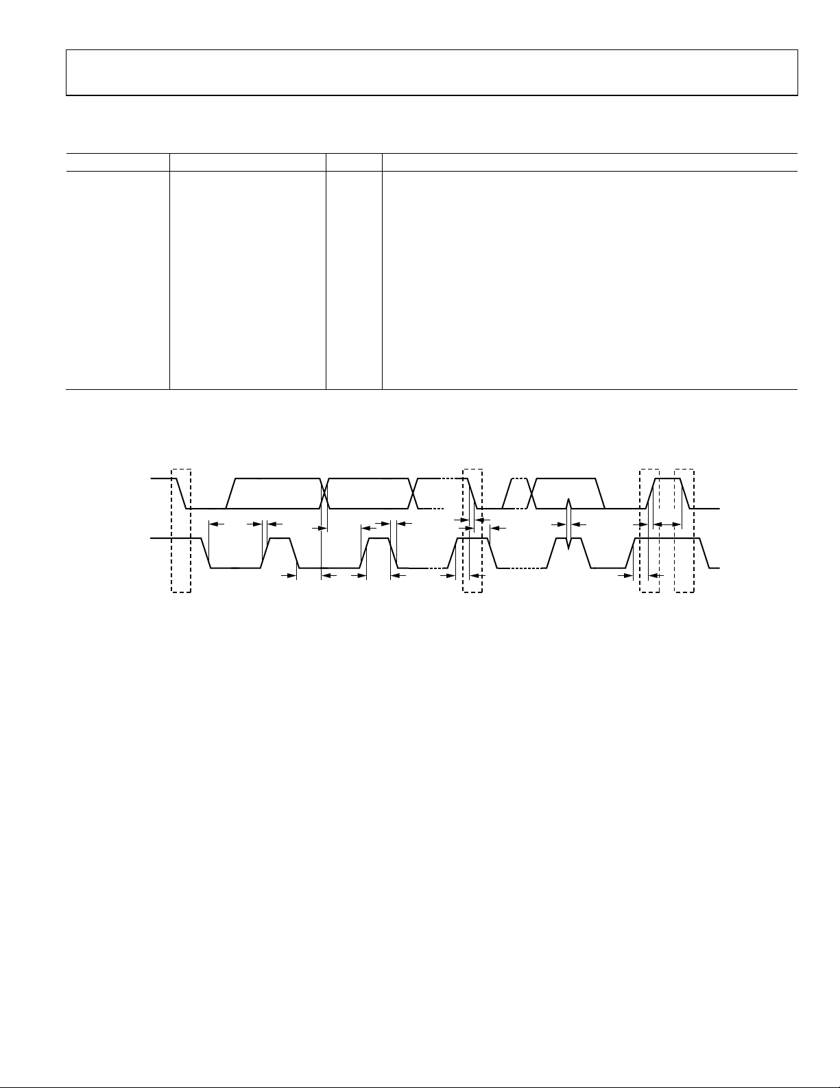
I2C-COMPATIBLE INTERFACE TIMING SPECIFICATIONS
Table 3.
Parameter1 Min Max Unit Description
f
SCL
t
HIGH
t
LOW
t
SU, DAT
t
0 0.9 μs Data hold time
HD, DAT
t
SU, STA
t
HD, STA
t
BUF
t
SU, STO
tR 20 + 0.1 C
tF 20 + 0.1 C
t
SP
CB 400 pF Capacitive load for each bus line
1
Guaranteed by design.
2
CB is the total capacitance of one bus line in picofarads.
400 kHz SCL clock frequency
0.6 μs SCL high time
1.3 μs SCL low time
100 ns Data setup time
0.6 μs Setup time for repeated start
0.6 μs Hold time for start/repeated start
1.3 μs Bus free time between a stop and a start condition
0.6 μs Setup time for stop condition
2
300 ns Rise time of SCL and SDA
B
B
300 ns Fall time of SCL and SDA
0 50 ns Pulse width of suppressed spike
SD
t
LOW
SCL
S
S = START CONDITION
Sr = REPEATED ST ART CONDITI ON
P = STOP CO NDITION
t
R
t
HD, DAT
t
SU, DAT
Figure 3. I
t
F
t
F
t
HIGH
2
C-Compatible Interface Timing Diagram
t
SU, STA
t
HD, STA
Sr P S
t
SP
t
SU, STO
t
BUF
t
R
08028-003
Rev. 0 | Page 5 of 24
Page 6
ADP1655
http://www.BDTIC.com/ADI
ABSOLUTE MAXIMUM RATINGS
Table 4.
Parameter Rating
VIN, SDA/EN2, SCL/EN1, I2C/EN,
STROBE, TORCH, TX_MASK to SGND
LED_OUT, SW, VOUT to SGND −0.3 V to +12 V
PGND to SGND −0.3 V to +0.3 V
VOUT to LED_OUT −0.3 V to +6 V
Ambient Temperature Range (TA) −40°C to +85°C
Junction Temperature Range (TJ) −40°C to +125°C
Storage Temperature JEDEC J-STD-020
ESD Human Body Model ±2000 V
ESD Charged Device Model ±1000 V
ESD Machine Model ±200 V
−0.3 V to +6 V
Stresses above those listed under Absolute Maximum Ratings
may cause permanent damage to the device. This is a stress
rating only; functional operation of the device at these or any
other conditions above those indicated in the operational
section of this specification is not implied. Exposure to absolute
maximum rating conditions for extended periods may affect
device reliability.
THERMAL DATA
The ADP1655 may be damaged if the junction temperature
limits are exceeded. Monitoring T
is within the specified temperature limits. In applications with
high power dissipation and poor thermal resistance, the maximum
T
may have to be derated. In applications with moderate power
A
dissipation and low PCB thermal resistance, the maximum T
can exceed the maximum limit as long as the T
fication limits. T
of the device is dependent on the TA, the power
J
dissipation (PD) of the device, and the junction-to-ambient
thermal resistance (θ
calculated from the T
= TA + (PD × θJA)
T
J
) of the package. Maximum TJ is
JA
and PD using the following formula:
A
does not guarantee that TJ
A
is within speci-
J
A
THERMAL RESISTANCE
θJA of the package is based on modeling and calculation using
a 4-layer board. θ
is highly dependent on the application and
JA
board layout. In applications where high maximum power dissipation exists, attention to thermal board design is required. The
value of θ
environmental conditions. The specified value of θ
may vary, depending on PCB material, layout, and
JA
is based
JA
on a 4-layer, 4 in × 3 in, 2 1/2 oz copper board, per JEDEC
standards. For more information, see the AN-617 Application
Note, MicroCSP
θ
is specified for a device mounted on a JEDEC 2S2P PCB.
JA
TM
Wafer Level Chip Scale Package.
Table 3. Thermal Resistance
Package Type θJA Unit
12-Ball WLCSP 75 °C/W
ESD CAUTION
Rev. 0 | Page 6 of 24
Page 7
ADP1655
http://www.BDTIC.com/ADI
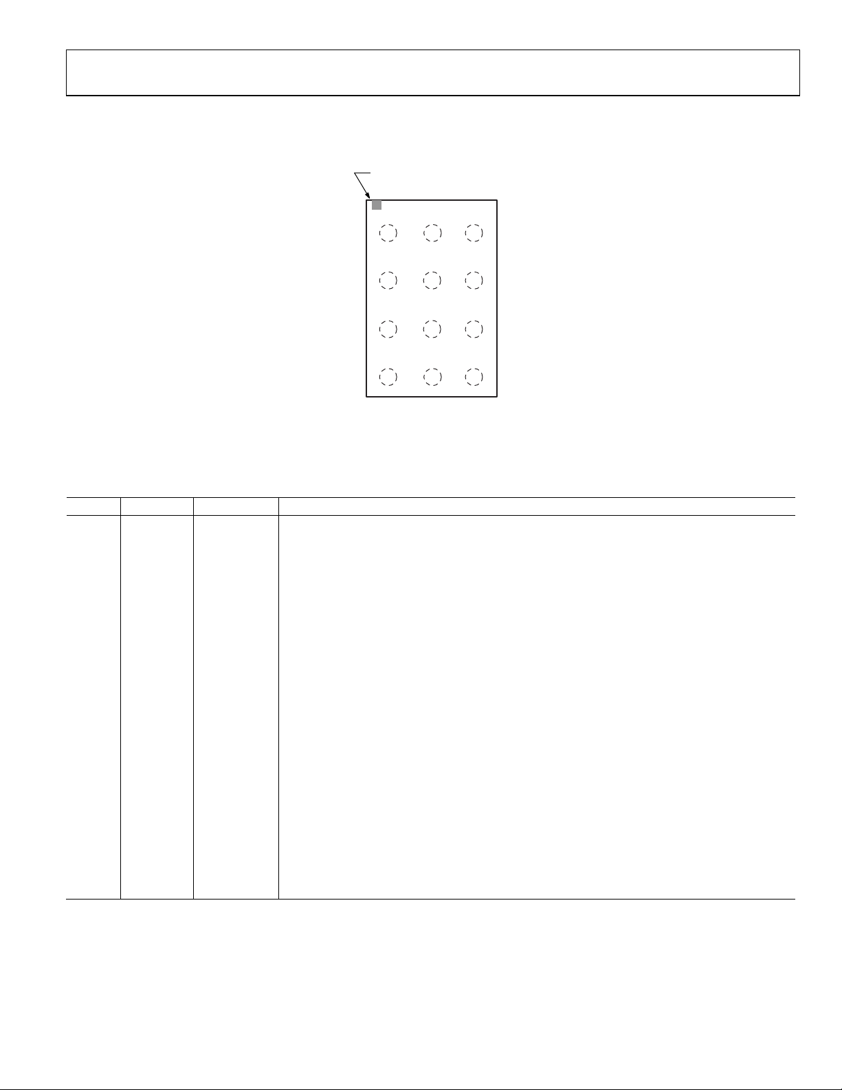
PIN CONFIGURATION AND FUNCTION DESCRIPTIONS
BALLA1
INDICATOR
1
PGND SGND VIN
A
23
SW
B
VOUT STROBE I2C/EN
C
LED_OUT SDA/EN2 SCL/EN1
D
(BALL SIDE DO WN)
Not to Scale
Figure 4. Pin Configuration
TORCH
TOP VIEW
TX_MASK
08028-004
Table 5. Pin Function Descriptions
Pin No. Mnemonic Type Description
A1 PGND Ground Ground for Internal Switching FET.
A2 SGND Ground Connect this pin at a single point to the power ground.
A3 VIN Supply
Connect the battery between VIN and PGND. Bypass VIN with a 10 μF, 6.3 V or greater X5R/X7R
capacitor.
B1 SW Output Connect a 2.2 μH inductor between SW and the battery.
B2 TORCH Digital Input This pin enables the torch, provided that the device is not in flash or assist light mode.
B3 TX_MASK Digital Input
Connect a digital signal to the TX_MASK pin. When the logic level is driven high during a flash
event the current is reduced to the torch level.
C1 VOUT Output
VOUT senses the output voltage of the boost converter and provides the input voltage to the LED
current source. The VOUT pin features a comparator to detect an overvoltage condition if the LED
string is open circuited. Connect a 10.0 μF capacitor between VOUT and PGND.
C2 STROBE
Digital Input/
Output
The STROBE input is used to synchronize the timing of the camera module to the LED driver in
2
I
C-compatible interface mode. In 2-bit logic interface mode, this acts as an output, indicating the
number of LEDs attached. STROBE = high indicates two LEDs, whereas STROBE = low indicates
one LED.
C3 I2C/EN Digital Input
A logic low selects the 2-bit logic interface, whereas logic high selects I
2
C-compatible interface. If
I2C/EN is low and SDA/EN2 and SCL/EN1 are low, the driver enters shutdown mode with
consumption < 1 μA.
D1 LED_OUT Output
White LED Anode Connection. Connect LED_OUT to the anode of the white LED. LED_OUT is
internally connected to a programmable PMOS current source, which regulates the LED current.
D2 SDA/EN2
D3 SCL/EN1 Digital Input
Digital Input/
Output
Data Input/Output (SDA). In 2-bit logic interface mode, SDA/EN2 is the second input bit of the
digital interface.
Second Input Bit (EN2). In I
Clock Input (SCL). In 2-bit logic interface mode, SCL/EN1 is the first input bit of the digital interface.
First Input Bit (EN1). In I
2
C mode, SDA is the data input/output of the I2C-compatible interface.
2
C mode, SCL is the clock input of the I2C-compatible interface.
Rev. 0 | Page 7 of 24
Page 8

ADP1655
http://www.BDTIC.com/ADI
TYPICAL PERFORMANCE CHARACTERISTICS
600
500
L = FDSE0312-2R2M
C
=10µF
OUT
Δ: 335 µs
400
(mA)
300
LED
I
200
I
100
0
INPUT VOLTAGE (V)
4.2 4.7 5.23.73.22.7
LIMIT
I
LIMIT
I
LIMIT
I
LIMIT
Figure 5. Maximum Current vs. Input Voltage, One LED
450
400
350
300
250
(mA)
200
LED
I
150
100
50
0
INPUT VOLTAG E (V)
4.2 4. 7 5. 23.73.22.7
I
LIMIT
I
LIMIT
I
LIMIT
I
LIMIT
Figure 6. Maximum Current vs. Input Voltage, Two LEDs;
LED Forward Voltage (Vf) = 4.3 V for each LED
L = FDSE0312-2R2M
C
=10µF
OUT
Δ: 335 µs
– 2.00A
– 1.75A
– 1.50A
– 1.25A
– 2.00A
– 1.75A
– 1.50A
– 1.25A
1
2
3
4
CHANNEL 1 (IL) 0.5A/DIV
08028-005
CHANNEL 2 (I
HPLED
Figure 8. Startup, Two LEDs Flash Mode, I
L = F DSE0312- 2R 2M
C
=10µF
OUT
1
2
3
4
CHANNEL
08028-006
CHANNEL 2 (I
1 (IL) 0.5A/DIV
HPLED
Figure 9. Startup, Two LEDs Assist Light Mode, I
L = FDSE0312-2R2M
C
=10µF
OUT
) 0.2A/DIV
Δ: 180µ s
) 0.2A/DIV
Δ: 180µ s
50µs/DIV
CHANNEL 3 (V
CHANNEL 4 (STRO BE) 5V/DIV
= 400 mA, VIN = 3.6 V
LED
50µs/DIV
CHANNEL 3 (V
CHANNEL 4 (SCL) 5V/ DIV
LED
) 5V/DIV
OUT
OUT
) 5V/DIV
08028-008
08028-009
= 40 mA, VIN = 3.2 V
1
2
3
4
50µs/DIV
CHANNEL
CHANNEL 2 (I
1 (IL) 0.5A/DIV
) 0.2A/DIV
HPLED
Figure 7. Startup, Two LEDs Flash Mode, I
CHANNEL 3 (V
CHANNEL 4 (STRO BE) 5V/DIV
OUT
= 400 mA, VIN = 3.2 V
LED
) 5V/DIV
08028-007
Rev. 0 | Page 8 of 24
1
2
3
4
50µs/DIV
CHANNEL 1 (IL) 0.5A/DIV
CHANNEL 2 (I
HPLED
) 0.2A/DIV
CHANNEL 3 (V
CHANNEL 4 (SCL) 5V/ DIV
Figure 10. Startup, Two LEDs Torch Mode, I
) 5V/DIV
OUT
= 40 mA, VIN = 3.6 V
LED
08028-010
Page 9

ADP1655
C
http://www.BDTIC.com/ADI
L = F D SE0312-2R 2M
C
=10µF
OUT
100
VIN = 3.2V
V
= 3.6V
IN
90
V
= 4.2V
IN
80
70
60
Y (%)
50
1
3
2
4
500ns/DIV
CHANNEL 1 (IL) 0.2A/DIV
CHANNEL 2 (I
HPLED
) 0.1A/DIV
CHANNEL 3 (LED_OUT) 5V/DIV
CHANNEL 4 (SW) 5V /DIV
Figu .6 V re 11. Inductor Current, Two LEDs Flash Mode, I
L = FDSE0312-2R2M
C
=10µF
OUT
1
2
3
4
500ns/DIV
CHANNEL
CHANNEL 2 (I
1 (IL) 0.2A/DIV
HPLED
) 0.02A/DIV
CHANNEL 3 (LED_OUT) 5V/DIV
CHANNEL 4 (SW) 5V/DIV
Figure 12. Inductor Current, Two LEDs Torch Mode, I
= 400 mA, VIN = 3
LED
= 40 mA, VIN = 3.6 V
LED
08028-011
08028-012
40
EFFICIEN
30
20
10
0
10 100
OUTPUT CURRENT (A)
Figure Series 14. Efficiency P
100
VIN = 3.2V
V
= 3.6V
IN
90
V
= 4.2V
IN
80
70
60
50
40
EFFICIENCY (%)
30
20
10
0
10 100 1k
Figure 15. Efficiency P
, Two High Power White LEDs in
LED/PIN
OUTPUT CURRENT (A)
, One High Power White LED
LED/PIN
1000
08028-014
08028-015
10
VIN = 3.2V
V
= 3.6V
IN
8
V
= 4.2V
IN
6
4
2
0
–2
ACCURACY (%)
LED
I
–4
–6
–8
–10
04300200100
OUTPUT CURRENT (mA)
Figure 13. LED Current Accuracy vs. Output Current
L = F D SE0312-2R 2M
C
OUT
1
2
3
4
00
500
CHANNEL 1 (IBAT) 1A/DIV
08028-013
CHANNEL 2 (I
Figure 16. Tx Masking Response, TX_MASK = 0 V to 1.8 V,
Rev. 0 | Page 9 of 24
=10µF
Δ:4µs
20µs/DIV
CHANNEL 3 (V
) 0.2A/DIV
HPLED
I
= 40 mA to 400 mA, VIN = 3.2 V
LED
CHANNEL 4 (TX_MAS K) 5V/DIV
OUT
) 5V/DIV
08028-016
Page 10

ADP1655
A
http://www.BDTIC.com/ADI
L = F DSE0312- 2R 2M
C
=10µF
OUT
1
2
3
4
CHANNEL 1 (IBAT) 1A/DIV
CHANNEL 2 (I
HPLED
) 0.2A/DIV
Δ: 260µs
100µs/DIV
CHANNEL 3 (V
CHANNEL 4 (TX_MASK) 5V/DIV
OUT
Figure 17. Tx Masking Response, TX_MASK = 1.8 V to 0 V,
I
= 40 mA to 400 mA, VIN = 3.2 V
LED
) 5V/DIV
08028-017
L = F DSE0312- 2R 2M
C
=10µF
OUT
Δ: 15m
1
CHANNEL 1 (VIN) 0.5V/DI V
CHANNEL 2 (I
HPLED
100µs/DIV
) 20mA/DIV
Figure 20. Line Transient, VIN = 3.2 V to 3.6 V, I
2.4
2.2
= 400 mA
LED
VIN = 3.2V
V
= 3.6V
IN
V
= 4.2V
IN
08028-020
1
2
3
200ms/DIV
CHANNEL
CHANNEL 2 (STRO BE) 1V/DIV
1 (I
HPLED
) 0.1A/DIV
CHANNEL 3 (SCL) 5V/DIV
8028-018
Figure 18. Assist Light and Flash, STROBE Edge Sensitive Mode, Two LEDs,
Timer = 850 ms, I
1
2
3
= 40 mA to 400 mA, VIN = 3.6 V
LED
2.0
1.8
1.6
PEAK CURRENT LIM IT (A)
1.4
1.2
–40 –20 0 20 40 60 80
TEMPERATURE (° C)
08028-021
Figure 21. Coil Peak Current Limit vs. Temperature, Output Mode Register =
00, 01, 10, and 11 (Binary)
1.2
VIN = 2.5V
V
= 3.6V
IN
V
= 4.5V
IN
1.0
0.8
0.6
0.4
SHUTDOWN CURRENT (µA)
0.2
200ms/DIV
CHANNEL 1 (I
CHANNEL 2 (STRO BE) 1V/DIV
HPLED
) 0.1A/DIV
CHANNEL 3 (SCL) 5V/DIV
Figure 19. Assist Light and Flash, STROBE Level Sensitive Mode, Two LEDs,
I
= 40 mA to 400 mA, VIN = 3.6 V
LED
8028-019
Rev. 0 | Page 10 of 24
0
–40 –20 0 20 40 60 80
TEMPERATURE (°C)
Figure 22. Shutdown Current vs. Temperature vs. VIN
08028-022
Page 11

ADP1655
(
http://www.BDTIC.com/ADI
7.0
VIN = 3.2V
V
= 3.6V
IN
V
= 4.2V
IN
6.5
6.0
5.5
(mA)
VIN
I
5.0
4.5
44
42
40
(mA)
LED
I
38
VIN = 3.0V
V
= 3.6V
IN
V
= 5.5V
IN
4.0
–40–200 20406080
TEMPERATURE (°C)
Figure 23. Operating Quiescent Current vs. Temperature, Torch Mode
4.0
3.5
3.0
µA)
2.5
2.0
1.5
STANDBY CURRENT
1.0
0.5
0
–40 –20 0 20 40 60 80 100 120
TEMPERATURE (°C)
VIN = 2.5V
V
= 3.6V
IN
V
= 4.5V
IN
Figure 24. Standby Current vs. Temperature vs. VIN,
I2C/EN = SCL/EN1 = SDA/EN2 = 1.8 V
2.15
2.10
VIN = 3.2V
V
= 3.6V
IN
V
= 4.2V
IN
36
–40–200 20406080100120
08028-023
TEMPERATURE (°C)
08028-026
Figure 26. LED Regulation, Set at 40 mA,
Current Set Register = 001 (Binary)
420
415
410
405
400
(mA)
LED
I
395
390
385
380
–40 –20 0 20 40 60 80 100 120
08028-024
TEMPERATURE (°C)
VIN = 3.0V
V
= 3.6V
IN
V
= 5.5V
IN
08028-027
Figure 27. LED Regulation, Set at 400 mA,
Current Set Register = 1010 (Binary)
2.05
2.00
1.95
SWITCHI NG FREQUENCY (MHz)
1.90
1.85
–40–200 20406080100120
TEMPERATURE (°C)
Figure 25. Switching Frequency vs. Temperature vs. VIN
08028-025
Rev. 0 | Page 11 of 24
Page 12

ADP1655
http://www.BDTIC.com/ADI
THEORY OF OPERATION
The ADP1655 is a high power, white LED driver ideal for
driving white LEDs for use as a camera flash. The ADP1655
includes a boost converter and a current regulator suitable
for powering one or two high power, white LEDs.
The ADP1655 responds to a 2-pin control interface that can
operate in two separate pin-selectable modes: tying the I2C/
EN pin high enables the I
2
C interface; tying the I2C/EN pin
low enables a 2-bit logic interface.
WHITE LED DRIVER
The ADP1655 drives a synchronous boost converter to power
one or two series-connected, high power LEDs. The white
LED driver regulates the high power LED current for accurate
brightness control. The ADP1655 uses an integrated PFET
current regulator.
When the white LED is turned on, the step-up converter output
voltage slew is limited to prevent excessive battery current while
charging the output capacitor. The output voltage of the boost
INPUT VOLTAGE = 2.5V TO 5.5V
L1
VIN
A3 B1 C1
SW
C
PGND
IN
converter is sensed at VOUT. If the output voltage exceeds
the 9.5 V (typical) limit, the white LED driver turns off and
indicates that a fault condition has occurred through the system
registers. This feature prevents damage due to an overvoltage if
the white LED string fails with an open-circuit condition.
Setting the LED regulation currents depends on the 2-pin
control interface used.
ASSIST LIGHT AND TORCH MODES
The ADP1655 features a programmable assist light mode that
provides continuous LED current. The STROBE pin or the 2-bit
logic interface can be used to transition from assist light mode
directly to flash mode. The TORCH pin provides an alternative
means of accessing a continuous LED current mode of operation. Both assist light and torch modes deliver the same current,
which is programmable via the I
C
OUT
PGND
VOUT
2
C-compatible interface.
I2C/EN
SCL/EN1
SDA/EN2
TORCH
STROBE
TX_MASK
2.5V
UVLO
PWM
C3
D3
D2
INTERFACE
B2
CONTROL
C2
B3
CONTROLLER
AND
CURRENT
SENSE
9.5V
OVP
FAULT
REGISTER
THERMAL
PROTECTION
DETECTOR
A1A2
PGNDSGND
PGNDAGND
COUT
HPLED
DRIVER
CURRENT
SENSE
4.35V
HPLED
SHORT
HIGH POW ER LED
CURRENT CONTROL
LED_OUT
D1
PGND
08028-029
Figure 28. Detailed Block Diagram
Rev. 0 | Page 12 of 24
Page 13

ADP1655
http://www.BDTIC.com/ADI
2-BIT LOGIC INTERFACE MODE (I2C/EN = 0)
In 2-bit logic interface mode, the two control pins, EN1 and
EN2, select whether the part is disabled or operating in assist
light mode or flash mode, as outlined in Ta b le 6. Additionally,
the TORCH pin selects torch mode.
Figure 29 illustrates state transitions of 2-bit logic mode controlled by digital inputs EN1, EN2, TORCH, and TX_MASK.
EN1 = 1
EN2 = 1
FLASH
EN1 = 1
EN1 = 0
EXTERNAL
TORCH
When the ADP1655 is in flash mode, the TX_MASK pin can
be used to reduce the battery load. The device remains in flash
mode, but the LED driver output current is reduced to the assist
light level.
Table 6. 2-Bit Logic Interface Mode Selection
Mode
Shutdown 0 0 0 0 0 mA
Torch 0 0 0 1
Assist light 0 0 1 X
Reserved 0 1 0 X 0 mA
Flash 0 1 1 X
EN1 = 0
EN2 = 1
TORCH = 0
TORCH = 1
Figure 29. 2-Bit Logic Mode State Transitions (I2C/EN = 0)
ASSIST
LIGHT
EN2 = 1
EN1 = 1
EN2 = 1
EN2 = 0
SHUTDOWN
EN1 = 0
EN2 = 0
TIMEOUT
I2C/
EN
EN1 EN2 TORCH Output Current
One LED: 80 mA
Two LEDs: 40 mA
One LED: 80 mA
Two LEDs: 40 mA
One LED: 500 mA
Two LEDs: 320 mA
08028-030
I2C INTERFACE MODE (I2C/EN = 1)
The ADP1655 includes an I2C-compatible serial interface for
control of the LED current, as well as for a readback of system
status registers. The I
0x61 in read mode.
2
Table 7. I
C Interface Mode Selection
Mode
Standby 1 X X 0 0 mA
Torch 1 X X 1 20 mA to 160 mA
Assist light 1 X X X 20 mA to 160 mA2
Flash 1 X X X 200 mA to 500 mA2
1
Torch mode has to be enabled from Register 0x04.
2
The output current value depends on the register settings.
Registers values are reset to the default values when VIN supply
falls below the undervoltage (UVLO) level.
Figure 30 illustrates the I
The subaddress content selects which of the five ADP1655
registers is written to first. The ADP1655 sends an acknowledgement to the master after the 8-bit data byte has been written.
The ADP1655 increments the subaddress automatically and starts
receiving a data byte to the following register until the master
sends an I
2
I
C read sequence of a single register. ADP1655 sends the data
2
C stop as shown in Figure 31. Figure 32 shows the
from the register denoted by the subaddress and increments
the subaddress automatically, sending data from the next register until the master sends an I
Figure 33.
State transitions between standby, assist light, flash, and
external torch modes are described in the State Transitions
section and Figure 34.
The register definitions are shown in the I
section. The lowest bit number (0) represents the least
significant bit, and the highest bit number (7) represents
the most significant bit.
2
C chip address is 0x60 in write mode and
I2C/
EN SCL SDA TORCH Output Current
2
C write sequence to a single register.
2
C stop condition as shown in
2
C Register Map
1, 2
Rev. 0 | Page 13 of 24
Page 14

ADP1655
http://www.BDTIC.com/ADI
0 = WRITE
S
01 100 00 0
T
CHIP ADDRESS
0
DP1655 ACK
Figure 30. I
SUBADDRESS
2
C Single Register Write Sequence
00
ADP1655 RECEIVES
DATA
ADP1655 ACK
MASTER
STOP
S
P
ADP1655 ACK
08028-032
0 = WRITE
S
01100 00 0
T
CHIP ADDRESS
0
ADP1655 ACK
SUBADDRESS
REGISTER N
00
ADP1655 ACK
Figure 31. I
ADP1655 RECEIVES
DATA TO REGISTER N
2
C Multiple Register Write Sequence
ADP1655 RECEIVES
DATA TO REGI STER N + 1
ADP1655 ACK
0
ADP1655 RECEIVES
DATA TO LAST REGISTER
ADP1655 ACK
MASTER
STOP
S
0
P
ADP1655 ACK
08028-033
MASTER
0 = WRITE 1 = READ
S
0110000 0
T
CHIP ADDRESS
SUBADDRESS
S
0
0110000 01 0
T
CHIP ADDRESS
ADP1655SENDS
DATA
STOP
10
S
P
ADP1655 ACK
Figure 32. I
ADP1655 ACK
2
C Single Register Read Sequence
ADP1655 ACK
MASTER ACK
08028-034
MASTER
0 = WRITE 1 = READ
S
0110000 0 0 00
T
CHIP ADDRESS CHIP AD DRESS
DP1655 ACK
SUBADDRESS
REGISTER N
S
0110000 01 0
T
DP1655 ACK
Figure 33. I
ADP1655 SENDS
DATA OF REG ISTER N
DP1655 ACK
2
C Multiple Register Read Sequence
ADP1655 SENDS
REGISTER N + 1
MASTER ACK
DATA OF
0
ADP1655 SENDS
DATA OF LAST
MASTER ACK
REGISTER
STOP
1
MASTER ACK
S
P
8028-035
Rev. 0 | Page 14 of 24
Page 15

ADP1655
http://www.BDTIC.com/ADI
STATE TRANSITIONS
When the ADP1655 is in flash mode, the TX_MASK pin can
be used to reduce the battery load. The device remains in flash
mode, but the LED driver output current is reduced to the assist
TX_MASK ENABLED
MODE = ASSIST LIGHT
light level. In Figure 34, if the flash was triggered by the strobe
pin in level-sensitive mode, a timeout triggers a timeout fault,
as defined in the Safety Features section.
TX_MASK = 1
OUTPUT ON
STROBE = 1
EXTERNAL
TORCH
OUTPUT ON
STROBE DISABL ED
MODE = FLASH
EN1 = 0
EN2 = 1
ASSIST
LIGHT
OUTPUT ON
MODE = ASSIST LIGHT
OUTPUT OFF
TORCH NOT
ALLOWE D
Figure 34. I
STROBE = 1
TX_MASK = 0
STROBE DISABLED
MODE = FLASH
TX_MASK = 0
TORCH = 0
2
C Interface Mode: State Transitions
TORCH ALLO WED
MODE = TORCH
FLASH
OUTPUT ON
STROBE = 1
OUTPUT ON
STROBE DISABL ED
MODE = FLAS H
STANDBY
I2C/EN = 1
TIMEOUT
OUTPUT OFF
8028-036
Rev. 0 | Page 15 of 24
Page 16

ADP1655
http://www.BDTIC.com/ADI
I2C REGISTER MAP
The lowest bit number (0) represents the least significant bit, and the highest bit number (7) represents the most significant bit.
Table 8. Design Information Register (Register 0x00)
Bit R/W Reset State
7:0 R 00100001
Table 9. Version Register (Register 0x01)
Bit R/W Reset State
7:0 R 00000001
Table 10. VREF and Timer Register (Register 0x02)
Bit R/W Description
7:6 R/W Reserved
5:4 R/W Number of LEDs detection comparator reference level
00 = 4.3 V (default)
01 = 4.6 V
10 = 4.0 V
11 = 4.9 V
3:0 R/W Flash timer value setting
0000 = 100 ms
0001 = 150 ms
0010 = 200 ms
0011 = 250 ms
0100 = 300 ms
0101 = 350 ms
0110 = 400 ms
0111 = 450 ms
1000 = 500 ms
1001 = 550 ms
1010 = 600 ms
1011 = 650 ms
1100 = 700 ms
1101 = 750 ms
1110 = 800 ms
1111 = 850 ms (default)
Rev. 0 | Page 16 of 24
Page 17

ADP1655
http://www.BDTIC.com/ADI
Table 11. Current Set Register (Register 0x03)
Bit R/W Description
7:4 R/W Flash current value setting
0000 = 200 mA
0001 = 220 mA
0010 = 240 mA
0011 = 260 mA
0100 = 280 mA
0101 = 300 mA
0110 = 320 mA (default for two LEDs)
0111 = 340 mA
1000 = 360 mA
1001 = 380 mA
1010 = 400 mA
1011 = 420 mA
1100 = 440 mA
1101 = 460 mA
1110 = 480 mA
1111 = 500 mA (default for one LED)
3 N/A
2:0 R/W Torch and assist light current value setting
000 = 20 mA
001 = 40 mA (default)
010 = 60 mA
011 = 80 mA
100 = 100 mA
101 = 120 mA
110 = 140 mA
111 = 160 mA
Table 12. Output Mode Register (Register 0x04)
Bit R/W Description
7:6 R/W Inductor peak current limit setting
00 = 1.25 A
01 = 1.5 A
10 = 1.75 A (default)
11 = 2.0 A
5 R/W 0 = edge sensitive
1 = level sensitive (default)
4 R/W 0 = TORCH not allowed
1 = TORCH allowed (default)
3 R/W 0 = LED_OUT off (default)
1 = LED_OUT on
2 R/W 0 = STROBE disabled
1 = STROBE enabled (default)
1:0 R/W Configures LED output mode
00 = standby mode (default)
01 = reserved
10 = assist light mode
11 = flash mode
Rev. 0 | Page 17 of 24
Page 18

ADP1655
http://www.BDTIC.com/ADI
Table 13. Fault Information Register (Register 0x05)
Bit R/W Description
7 R 0 = no fault (default)
1 = overvoltage or C
6 R 0 = no fault (default)
1 = short-circuit fault
5 R 0 = no fault (default)
1 = overtemperature fault
4 R 0 = no fault (default)
1 = timeout 850 ms fault
3 R/W 0 = one LED
1 = two LEDs (default)
2 R Reserved
1 R 0 = no fault (default)
1 = current limit fault
0 R Reserved
Table 14. Input Control Register (Register 0x06)
Bit R/W Description
7:3 Reserved
2 R/W 0 = Strobe 0 triggers flash in level sensitive mode, Strobe 1 > 0 triggers flash in edge sensitive mode
1 = Strobe 1 triggers flash in level sensitive mode, Strobe 0 > 1 triggers flash in edge sensitive mode (default)
1 R/W 0 = TX_MASK function disabled
1 = TX_MASK function allowed (default)
0 R Reserved
OUT
fault
Rev. 0 | Page 18 of 24
Page 19

ADP1655
http://www.BDTIC.com/ADI
SAFETY FEATURES
For critical system conditions, such as output overvoltage,
flash timeout, LED output short circuit, and overtemperature
conditions, the ADP1655 has built-in safety mechanisms. If
one of the fault conditions occurs, the device shuts down and
a corresponding flag is set in the fault information register
(Register 0x05). In I
processor can read the fault information register through the
2
I
C interface to determine the nature of the fault condition
and, consequently, the fault flag is cleared. The device is
disabled until the fault information register is cleared.
In 2-bit logic interface mode, the I
available. To clear a fault, set EN1, EN2, and TORCH low.
2
C interface mode, the system baseband
2
C register readback is not
OVERVOLTAGE FAULT
The ADP1655 contains a comparator at the VOUT pin that
monitors the voltage between VOUT and SGND. If the voltage
exceeds 9.5 V (typical), the ADP1655 shuts down. In I
Bit 7 in the fault information register is read back as high. The
ADP1655 is disabled until the fault is cleared, ensuring protection against an open circuit.
2
C mode,
OUTPUT CAPACITOR FAULT
If no output capacitor is present at the VOUT pin when the
ADP1655 is enabled for a flash, torch, or assist light event,
the part shuts down and Bit 7 in the fault information register
is read back as high. The ADP1655 is disabled until the fault is
cleared. The output capacitor detection scheme does not cause
the VOUT pin to rise above the overvoltage threshold even though
the overvoltage flag (Bit 7) in the fault information register
(Register 5) is set. The overvoltage and output capacitor fault
flags share a single register bit to reduce the required number
of registers.
TIMEOUT FAULT
If the 2-bit logic interface is used, the maximum duration for
flash being enabled (EN1/EN2 = 1) is preset to 850 ms. If EN1
and EN2 remain high for longer than 850 ms, ADP1655 is
disabled until the fault is cleared (EN1, EN2, and TORCH low).
2
In I
C mode, if strobe mode is enabled (Register 0x04, Bit 2),
strobe is set to level sensitive mode (Register 0x04, Bit 5), and
if strobe remains high for longer than 850 ms, the timeout fault
bit, Register 0x05, Bit 4), is read back as high. The ADP1655 is
disabled until the fault is cleared.
OVERTEMPERATURE FAULT
If the junction temperature of the ADP1655 rises above 150°C,
a thermal protection circuit shuts down the device. In I
Bit 5 of the fault information register is read back as high. The
ADP1655 is disabled until the fault is cleared.
2
C mode,
SHORT-CIRCUIT FAULT
The LED_OUT pin features short-circuit protection that
disables the ADP1655 if it detects a short circuit to ground at
the LED_OUT pin. The ADP1655 monitors the LED voltage
when the LED driver is enabled. If the LED_OUT pin remains
below the short-circuit detection threshold during startup, a
short circuit is detected. Bit 6 of the fault information register
is read back as high. The ADP1655 is disabled until the fault is
cleared.
CURRENT LIMIT
The internal switch limits battery current by ensuring that the
peak inductor current does not exceed the programmed limit
(current limit is set by Bit 6 and Bit 7 in the output mode register,
Register 0x04). If the peak inductor current exceeds the limit,
the part shuts down and Bit 1 of the fault information register
is read back as high. The ADP1655 is disabled until the fault is
cleared.
AMOUNT OF LED DETECTION
The ADP1655 is able to detect the amount of LED connected in
series between the LED_OUT pin and the PGND potential. In
2
I
C mode, the detection is enabled with Bit 3 in the output mode
register. The part uses an 80 mA LED driver current setting to
detect the LED forward voltage (Vf) with a voltage comparator
at the start of a flash, torch, or assist light event. If the detected
forward voltage is higher than 4.3 V (typical), Bit 3 of the fault
information register is read back as high.
INPUT UNDERVOLTAGE
The ADP1655 includes an input undervoltage lockout circuit. If
the battery voltage drops below the 2.4 V (typical) input UVLO
threshold, the ADP1655 shuts down. In this case, information
in all registers is lost, and when power is reapplied, a power-on
reset circuit resets the registers to their default conditions.
Rev. 0 | Page 19 of 24
Page 20

ADP1655
http://www.BDTIC.com/ADI
APPLICATIONS INFORMATION
EXTERNAL COMPONENT SELECTION
Selecting the Inductor
The ADP1655 boost converter increases the battery voltage
to allow driving of one or two LEDs, whose combined voltage
drop is higher than the battery voltage plus the current source
headroom voltage. This allows the converter to regulate the
LED current over the entire battery voltage range and with a
wide variation of LED forward voltage.
The inductor saturation current should be greater than the sum
of the dc input current and half the inductor ripple current. A
reduction in the effective inductance due to saturation increases
the inductor current ripple. Suggested inductors are shown in
Tabl e 15 .
Table 15. Suggested Inductors
Value
Vendo r
Toko 2.2 FDSE0312 160 3.1 3 × 3 × 1.2
Toko 2.0 DE2812C 67 1.8 3.0 × 3.2 × 1.22
Coilcraft 2.2 LPS3010 220 1.4 3 × 3 × 1.0
Coilcraft 2.2 LPS3314 100 1.5 3 × 3 × 1.4
(µH) Part No.
Selecting the Input Capacitor
The ADP1655 requires an input bypass capacitor to supply
transient currents while maintaining constant input and output
voltages. The input capacitor carries the input ripple current,
allowing the input power source to supply only the dc current.
Use an input capacitor with a sufficient ripple current rating to
handle the inductor ripple. Increased input capacitance reduces
the amplitude of the switching frequency ripple on the battery.
Because of the dc bias characteristics of ceramic capacitors, a
0603, 6.3 V X5R/X7R, 10 µF ceramic capacitor is preferable.
Higher value input capacitors help to reduce the input voltage
ripple and improve transient response. Maximum input
capacitor current is calculated using the following equation:
≥
II
CIN
)(
MAXLOAD
OUT
IN
V
DCR
(mΩ)
IN
ISAT
Dimensions
(A)
L × W × H (mm)
VVV )( −
OUT
To minimize supply noise, place the input capacitor as close to
the VIN pin of the ADP1655 as possible. As with the output
capacitor, a low ESR capacitor is suggested. A list of suggested
input capacitors is shown in Tab le 1 6 .
Table 16. Suggested Input Capacitors
Vendor Value Part No.
Murata 10 μF, 6.3 V GRM188R60J106ME47 1.6 × 0.8 × 0.8
TDK 10 μF, 6.3 V C1608JB0J106K 1.6 × 0.8 × 0.8
Tayio
Yuden
10 μF, 6.3 V JMK107BJ106MA 1.6 × 0.8 × 0.8
Dimensions
L × W × H (mm)
Selecting the Output Capacitor
The output capacitor maintains the output voltage and supplies
the LED current during NFET power switch on period. It also
stabilizes the loop. A 10.0 µF, 16 V X5R/X7R ceramic capacitor
is suggested.
Note that dc bias characterization data is available from capacitor manufacturers and should be taken into account when
selecting input and output capacitors. 16 V capacitors are
recommended for most two-LED designs. Designs with 1 mm
height restrictions can also use 0603 case size, 16 V capacitors
in parallel. A list of suggested output capacitors is shown in
Tabl e 17 .
Table 17. Suggested Output Capacitors
Vendor Value Part No.
Murata 10.0 μF, 10 V GRM21BR71A106KE51 2 × 1.25 × 1.25
Murata 10.0 μF, 16 V GRM31CR61C106KA88 3.2 × 1.6 × 1.6
Tayio
Yuden
10.0 μF, 16 V EMK212BJ106KG 2 × 1.25 × 1.25
Dimensions
L × W × H (mm)
Higher output capacitor values reduce the output voltage ripple
and improve load transient response. When choosing this value,
it is also important to account for the loss of capacitance due to
output voltage dc bias.
Ceramic capacitors are manufactured with a variety of dielectrics, each with different behavior over temperature and applied
voltage. Capacitors must have a dielectric that ensures the
minimum capacitance over the necessary temperature range
and dc bias conditions. X5R or X7R dielectrics with a voltage
rating of 10.0 V or 16 V are suggested for best performance.
Y5V and Z5U dielectrics are not suggested for use with any
dc-to-dc converter because of their poor temperature and dc
bias characteristics.
Rev. 0 | Page 20 of 24
Page 21

ADP1655
A
I
E
http://www.BDTIC.com/ADI
The worst-case capacitance accounting for capacitor variation
over temperature, component tolerance, and voltage is calculated using the following equation:
= C
C
EFF
× (1 − TEMPCO) × (1 − TOL)
OUT
where:
is the effective capacitance at the operating voltage.
C
EFF
TEMPCO is the worst-case capacitor temperature coefficient.
TOL is the worst-case component tolerance.
In this example, TEMPCO over −40°C to +85°C is assumed to
be 15% for an X5R dielectric, TOL is assumed to be 10%, and
C
is 9.528 F at 1.8 V, as shown in Figure 35.
OUT
Substituting these values in the equation yields
C
= 9.528 F × (1 − 0.15) × (1 − 0.1) = 7.288 F
EFF
12
10
8
6
To guarantee the performance of the ADP1655, it is imperative
that the effects of dc bias, temperature, and tolerances on the
behavior of the capacitors be evaluated for each application.
The peak-to-peak output voltage ripple for the selected output
capacitor and inductor values is calculated using the following
equation:
V
RIPPLE
V
SW
IN
CLf
××××π
=
()
OUT
RIPPLE
=
822
SW
Cf
××
OUT
Capacitors with lower equivalent series resistance (ESR) are
preferred to guarantee low output voltage ripple, as shown in
the following equation:
V
ESR ≤
COUT
RIPPLE
I
RIPPL
The effective capacitance needed for stability, which includes
temperature and dc bias effects, is 4 µF.
PACITANCE (µF)
4
C
2
0
0 2 4 6 8 10121416
DC BIAS VOLTAGE (V)
Figure 35. DC Bias Characteristic of a 16 V, 10 μF Ceramic Capacitor
08028-037
Rev. 0 | Page 21 of 24
Page 22

ADP1655
http://www.BDTIC.com/ADI
PCB LAYOUT
Poor layout can affect performance, causing electromagnetic
interference (EMI) and electromagnetic compatibility (EMC)
problems, ground bounce, and voltage losses. Poor layout can
also affect regulation and stability. A good layout is implemented
using the following rules and shown in Figure 36:
• Place the inductor, input capacitor, and output capacitor
close to the IC using short tracks. These components carry
high switching frequencies and large tracks act as antennas.
V
IN
INPUT
CAPACITO R
PGND
• Route the output voltage path away from the inductor and
SW node to minimize noise and magnetic interference.
• Maximize the size of ground metal on the component side
to help with thermal dissipation.
• Use a ground plane with several vias connecting to the
component side ground to further reduce noise interference on sensitive circuit nodes.
PGND
HIGH
POWER
LED
INDUCTOR
CAPACITO R
Figure 36. Example Layout of the ADP1655 Driving Two White LEDs
OUTPUT
ADP1655
HIGH
POWER
LED
8028-028
Rev. 0 | Page 22 of 24
Page 23

ADP1655
http://www.BDTIC.com/ADI
OUTLINE DIMENSIONS
0.660
0.602
0.544
SEATING
PLANE
0.330
0.310
0.290
1.50
REF
3
2
1
A
B
C
BALL A1
IDENTIFIER
1.54
1.50
1.46
2.04
2.00
1.96
0.022
REF
D
020409-B
TOP VIEW
(BALL SIDE DOWN)
0.380
0.352
0.324
0.04 MAX
COPLANARITY
0.280
0.250
0.220
0.50
REF
1.00
REF
BOTTOM VIEW
(BALL SI DE UP)
Figure 37. 12-Ball Wafer Level Chip Scale Package [WLCSP]
(CB-12-4)
Dimensions shown in millimeters
ORDERING GUIDE
Model Temperature Range Package Description Package Option Branding
ADP1655ACBZ-R71 –40°C to +125°C 12-Ball Wafer Level Chip Scale Package [WLCSP] CB-12-4 LAM
ADP1655-EVALZ1 Evaluation Board
1
Z = RoHS Compliant Part.
Rev. 0 | Page 23 of 24
 Loading...