

Page 1
1.5 A LED Flash Driver with
V
T
FEATURES
Ultracompact solution
Small, 2 mm × 1.5 mm, 12-ball WLCSP package
Thin, 3 mm × 3 mm × 0.75 mm, 10-lead LFCSP package
Smallest footprint, 1 mm height, 1 H power inductor
LED current source for local LED grounding
Simplified routing to/from LED
Improved LED thermals
Synchronous 3 MHz PWM boost converter, no external diode
High efficiency: 90% peak
Reduces high levels of input battery current during flash
Limits battery current drain in torch mode
2
I
C programmable
Currents up to 1500 mA in flash mode for 1 LED with
±7% accuracy over all conditions
Currents up to 200 mA in torch mode
Programmable dc battery current limit (4 settings)
Programmable flash timer up to 1600 ms
Low VBAT mode to reduce LED current automatically
4-bit ADC for LED V
Control
2
I
C-compatible control registers
External STROBE and torch input pins
2 transmitter mask (TxMASK) inputs
Safety
Thermal overload protection
Inductor fault detection
LED short-/open-circuit protection
APPLICATIONS
Camera-enabled cellular phones and smart phones
Digital still cameras, camcorders, and PDAs
, die/LED temperature readback
F
I2C-Compatible Interface
ADP1650
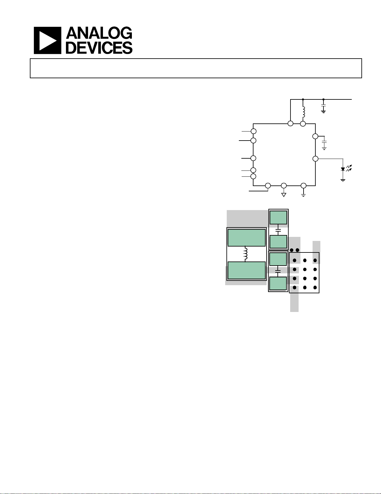
FUNCTIONAL BLOCK DIAGRAM
INPUT VO LTAGE = 2.7V TO 5.0
1.0µH
VIN
LED_OUT
PGND
LED
ANODE
SW
VOUT
PGND
Li-ION +
TX1/TORCH
X2/ILED/ADC
L1
AREA = 16.4mm
GPIO1
GPIO2
ADP1650
STROBE
SCL
SDA
EN SGND
Li-ION +
INDUCTOR
2
Figure 2. PCB Layout (WLCSP)
Figure 1.
1
C
C2
10µF
10µF
MAX 1.5A
DIGITAL
INPUT/
OUTPUT
08837-001
8837-002
GENERAL DESCRIPTION
The ADP1650 is a very compact, highly efficient, single white
LED flash driver for high resolution camera phones that
improves picture and video quality in low light environments.
The device integrates a programmable 1.5 MHz or 3 MHz
synchronous inductive boost converter, an I
2
C-compatible
interface, and a 1500 mA current source. The high switching
frequency enables the use of a tiny, 1 mm high, low cost, 1 µH
power inductor, and the current source permits LED cathode
grounding for thermally enhanced, low EMI, and compact
layouts.
The LED driver maximizes efficiency over the entire battery
voltage range to maximize the input-power-to-LED-power
conversion and to minimize battery current draw during flash
Rev. C
Information furnished by Analog Devices is believed to be accurate and reliable. However, no
responsibility is assumed by Anal og Devices for its use, nor for any infringements of patents or ot her
rights of third parties that may result from its use. Specifications subject to change without notice. No
license is granted by implication or otherwise under any patent or patent rights of Analog Devices.
Trademarks and registered trademarks are the property of their respective owners.
events. A programmable dc battery current limit safely maximizes
LED current for all LED V
and battery voltage conditions.
F
Two independent TxMASK inputs permit the flash LED current
and battery current to reduce quickly during a power amplifier
current burst. The I
2
C-compatible interface enables the programmability of timers, currents, and status bit readback for
operation monitoring and safety control.
The ADP1650 is available in a compact 12-ball, 0.5 mm pitch
WLCSP package and a 10-lead LFCSP package, and operates
within specification over the full −40°C to +125°C junction
temperature range.
One Technology Way, P.O. Box 9106, Norwood, MA 02062-9106, U.S.A.
Tel: 781.329.4700 www.analog.com
Fax: 781.461.3113 ©2010–2011 Analog Devices, Inc. All rights reserved.
Page 2

ADP1650
TABLE OF CONTENTS
Features.............................................................................................. 1
Applications....................................................................................... 1
Functional Block Diagram .............................................................. 1
General Description ......................................................................... 1
Revision History ............................................................................... 2
Specifications..................................................................................... 3
Recommended Specifications: Input and Output Capacitance
and Inductance ............................................................................. 5
I2C-Compatible Interface Timing Specifications ..................... 5
Absolute Maximum Ratings............................................................ 6
Thermal Data ................................................................................ 6
Thermal Resistance ...................................................................... 6
ESD Caution.................................................................................. 6
Pin Configurations and Function Descriptions ........................... 7
Typical Performance Characteristics ............................................. 8
Theory of Operation ...................................................................... 12
White LED Driver ...................................................................... 12
Modes of Operation ................................................................... 12
Assist Light.................................................................................. 13
Flash Mode .................................................................................. 13
Assist-to-Flash Operation ......................................................... 13
Torch Mode .................................................................................13
Torch-to-Flash Mode................................................................. 14
TxMASK Operation................................................................... 14
Frequency Foldback................................................................... 14
Indicator LED Driver................................................................. 14
Low Battery LED Current Foldback........................................ 14
Programmable Battery DC Current Limit.............................. 15
Analog-to-Digital Converter Operation................................. 15
5 V Output Operation ............................................................... 16
Safety Features................................................................................. 18
Short-Circuit Fault..................................................................... 18
Overvoltage Fault ....................................................................... 18
Dynamic Overvoltage Mode (DOVP) .................................... 18
Timeout Fault.............................................................................. 18
Overtemperature Fault.............................................................. 18
Indicator LED Fault ................................................................... 18
Current Limit.............................................................................. 18
Input Undervoltage.................................................................... 18
Soft Start ...................................................................................... 18
Reset Using the Enable (EN) Pin ............................................. 18
Clearing Faults............................................................................ 18
I2C Interface ................................................................................ 19
I2C Register Map............................................................................. 20
Applications Information.............................................................. 26
External Component Selection ................................................ 26
PCB Layout...................................................................................... 28
Outline Dimensions....................................................................... 29
Ordering Guide .......................................................................... 29
REVISION HISTORY
4/11—Rev. B to Rev. C
Added 10-Lead LFCSP Package........................................Universal
Changes to Features Section, General Description Section, and
Figure 2 Caption ............................................................................... 1
Changes to Table 1............................................................................ 3
Changes to Table 5............................................................................ 6
Added Figure 5; Renumbered Sequentially .................................. 7
Changes to Table 6............................................................................ 7
Changes to PCB Layout Section and Figure 45 Caption........... 28
Added Figure 46.............................................................................. 28
Updated Outline Dimensions....................................................... 29
Changes to Ordering Guide.......................................................... 29
2/11—Rev. A to Rev. B
Changes to Features Section and General Description Section . 1
Changes to Switching Regulator, Voltage Output Mode, VOUT
Voltage Parameter and Digital Inputs/GPIO, Torch Glitch
Filtering Delay Parameter, Table 1.................................................. 3
Rev. C | Page 2 of 32
Changed GND to Power Ground Throughout .............................6
Changed IL to I
IBAT to I
Change to Figure 10 Caption...........................................................8
Change to Figure 11 Caption...........................................................9
Changed LED_MOD = 10 to LED_MOD = 11 in Figure 32 ... 14
Changes to Analog-to-Digital Converter Operation Section and
Figure 37 .......................................................................................... 15
Changes to Selecting the Output Capacitor Section.................. 26
6/10—Rev. 0 to Rev. A
Changes to Contact Information.....................................................1
5/10—Revision 0: Initial Version
, ILED to I
L
Throughout..................................................................8
BAT
, LED OUT to LED_OUT, and
LED
Page 3

ADP1650
SPECIFICATIONS
1
V
= 3.6 V, TJ = −40°C to +125°C for minimum/maximum specifications, and TA = 25°C for typical specifications, unless otherwise noted.
IN
Table 1.
Parameter2 Conditions Min Typ Max Unit
SUPPLY
Input Voltage Range 2.7 5.0 V
Undervoltage Lockout Threshold VIN falling 2.3 2.4 2.5 V
Undervoltage Lockout Hysteresis 50 100 150 mV
Shutdown Current (IQ), EN = 0 V TJ = −40°C to +85°C, current into VIN pin, VIN = 2.7 V to 4.5 V 0.2 1 μA
Standby Current (I
Operating Quiescent Current Torch mode, LED current = 100 mA 5.3 mA
SW Switch Leakage TJ = −40°C to +85°C, V
T
LED DRIVER
LED Current
Assist Light, Torch Assist light value setting = 0 (000 binary) 25 mA
Assist light value setting = 7 (111 binary) 200 mA
Flash Flash value setting = 0 (00000 binary) 300 mA
Flash value setting = 24 (11000 binary) 1500 mA
LED Current Error—WLCSP I
I
I
I
LED Current Error—LFCSP I
I
I
I
LED Current Source Headroom—WLCSP Flash, 1200 mA LED current 290 mV
Torch, 200 mA LED current 190 mV
LED Current Source Headroom—LFCSP Flash, 1200 mA LED current 370 mV
Torch, 200 mA LED current 220 mV
LED_OUT Ramp-Up Time 0.6 ms
LED_OUT Ramp-Down Time 0.1 ms
SWITCHING REGULATOR
Switching Frequency Switching frequency = 3 MHz 2.8 3 3.2 MHz
Switching frequency = 1.5 MHz 1.4 1.5 1.6 MHz
Minimum Duty Cycle Switching frequency = 3 MHz 14 %
Switching frequency = 1.5 MHz 7 %
nFET Resistance—WLCSP 60 mΩ
pFET Resistance—WLCSP 50 mΩ
nFET Resistance—LFCSP 77 mΩ
pFET Resistance—LFCSP 85 mΩ
Voltage Output Mode
VOUT Voltage—WLCSP 4.575 5.000 5.425 V
VOUT Voltage—LFCSP 4.575 5.000 5.500 V
Output Current 500 mA
Line Regulation I
Load Regulation −0.7 %/A
), EN = 1.8 V TJ = −40°C to +85°C, current into VIN pin, VIN = 2.7 V to 4.5 V 3 10 μA
STBY
3
= 4.5 V 2 μA
= 25°C, V
J
= 700 mA to 1100 mA −6 +6 %
LED
= 300 mA to 650 mA, 1150 mA to 1500 mA −7 +7 %
LED
= 75 mA to 200 mA −10 +10 %
LED
= 25 mA to 50 mA −15 +15 %
LED
= 700 mA to 1100 mA −6 +6 %
LED
= 300 mA to 650 mA, 1150 mA to 1500 mA −7 +7 %
LED
= 75 mA to 200 mA −10 +10 %
LED
= 25 mA to 50 mA −15 +18 %
LED
at VOUT = 300 mA 0.3 %/V
LOAD
3
SW
SW
= 4.5 V 0.5 μA
Rev. C | Page 3 of 32
Page 4

ADP1650
Parameter2 Conditions Min Typ Max Unit
Pass-Through Mode Transition, Flash
VIN to LED_OUT, Entry 1200 mA LED current 580 mV
VIN to LED_OUT, Exit 1200 mA LED current 435 mV
Pass-Through Mode Transition, Torch
VIN to LED_OUT, Entry 200 mA LED current 380 mV
VIN to LED_OUT, Exit 200 mA LED current 285 mV
DIGITAL INPUTS/GPIO
Input Logic Low Voltage 0.54 V
Input Logic High Voltage 1.26 V
GPIO1, GPIO2, STROBE Pull-Down 390 kΩ
Torch Glitch Filtering Delay From torch rising edge to device start 5.5 7 7.5 ms
INDICATOR LED
LED Current Accuracy −22 +22 %
Short-Circuit Detection Threshold 1.2 V
Open-Circuit Detection Threshold 2.45 V
ADC
Resolution 4 Bits
Error External voltage mode 0 ±1 LSB
V
V
Input Voltage Range, GPIO2 External voltage mode 0 0. 5 V
SAFETY FEATURES
Maximum Timeout For Flash 1600 ms
Timer Accuracy −7.0 +7.0 %
DC Current Limit DC current value setting = 0 (00 binary) 1.35 1.5 1.65 A
DC current value setting = 1 (01 binary) 1.55 1.75 1.95 A
DC current value setting = 2 (10 binary) 1.8 2.0 2.2 A
DC current value setting = 3 (11 binary) 2.02 2.25 2.5 A
Low VBAT Mode Transition Voltage
Error 3.2 %
Hysteresis 50 mV
Coil Peak Current Limit Peak current value setting = 0 (00 binary) 1.55 1.75 1.95 A
Peak current value setting = 1 (01 binary) 2.02 2.25 2.5 A
Peak current value setting = 2 (10 binary) 2.47 2.75 3.0 A
Peak current value setting = 3 (11 binary) 2.7 3.0 3.3 A
Overvoltage Detection Threshold 5.15 5.5 5.9 V
LED_OUT Short-Circuit Detection
Comparator Reference Voltage
Thermal Shutdown Threshold
TJ Rising 150 °C
TJ Falling 140 °C
1
VIN is the input voltage to the circuit.
2
All limits at temperature extremes are guaranteed via correlation using standard statistical quality control (SQC).
3
VSW is the voltage on the SW switch pin.
mode, TJ = 25°C ±1 LSB
F
mode, TJ = −40°C to +125°C ±1.5 LSB
F
1.2 1.3 V
Rev. C | Page 4 of 32
Page 5
ADP1650
A
RECOMMENDED SPECIFICATIONS: INPUT AND OUTPUT CAPACITANCE AND INDUCTANCE
Table 2.
Parameter Symbol Conditions Min Typ Max Unit
CAPACITANCE C
Input TA = −40°C to +125°C 4.0 10 μF
Output TA = −40°C to +125°C 3.0 10 20 μF
MINIMUM AND MAXIMUM INDUCTANCE L TA = −40°C to +125°C 0.6 1.0 1.5 μH
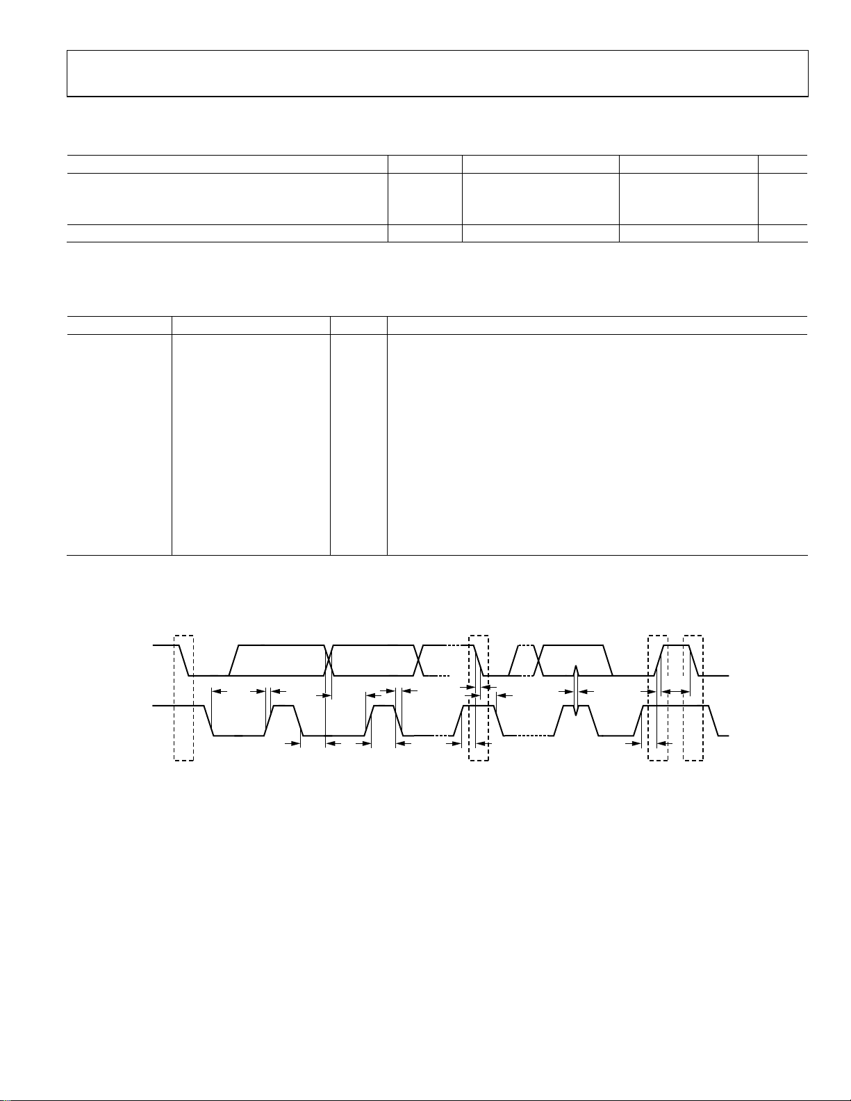
I2C-COMPATIBLE INTERFACE TIMING SPECIFICATIONS
Table 3.
Parameter1 Min Max Unit Description
f
SCL
t
HIGH
t
LOW
t
SU, DAT
t
0 0.9 μs Data hold time
HD, DAT
t
SU, STA
t
HD, STA
t
BUF
t
SU, STO
tR 20 + 0.1 C
tF 20 + 0.1 C
t
SP
2
C
400 pF Capacitive load for each bus line
B
1
Guaranteed by design.
2
CB is the total capacitance of one bus line in picofarads.
400 kHz SCL clock frequency
0.6 μs SCL high time
1.3 μs SCL low time
100 ns Data setup time
0.6 μs Setup time for repeated start
0.6 μs Hold time for start/repeated start
1.3 μs Bus free time between a stop and a start condition
0.6 μs Setup time for stop condition
2
300 ns Rise time of SCL and SDA
B
2
B
300 ns Fall time of SCL and SDA
0 50 ns Pulse width of suppressed spike
MIN
SD
t
LOW
SCL
S
S = START CONDI TION
Sr = REPEATED START CONDITIO N
P = STOP CONDITION
t
R
t
HD, DAT
t
SU, DAT
Figure 3. I
t
F
t
F
t
HIGH
2
C-Compatible Interface Timing Diagram
t
SU, STA
t
HD, STA
Sr P S
Rev. C | Page 5 of 32
t
SP
t
SU, STO
t
BUF
t
R
08837-003
Page 6
ADP1650
ABSOLUTE MAXIMUM RATINGS
Table 4.
Parameter Rating
VIN, SDA, SCL, EN, GPIO1, GPIO2, STROBE,
LED_OUT, SW, VOUT to Power Ground
PGND to SGND −0.3 V to +0.3 V
Ambient Temperature Range (TA) −40°C to +85°C
Junction Temperature Range (TJ) −40°C to +125°C
Storage Temperature JEDEC J-STD-020
ESD Human Body Model ±2000 V
ESD Charged Device Model ±500 V
ESD Machine Model ±150 V
−0.3 V to +6 V
THERMAL RESISTANCE
θJA of the package is based on modeling and calculation using
a 4-layer board. θ
board layout. In applications where high maximum power dissipation exists, attention to thermal board design is required. The
value of θ
JA
environmental conditions. The specified value of θ
on a 4-layer, 4 in × 3 in, 2 ½ oz copper board, per JEDEC
standards. For more information, see the AN-617 Application
Note, MicroCSP™ Wafer Level Chip Scale Package.
θ
is specified for a device mounted on a JEDEC 2S2P PCB.
JA
is highly dependent on the application and
JA
may vary, depending on PCB material, layout, and
is based
JA
Stresses above those listed under Absolute Maximum Ratings
may cause permanent damage to the device. This is a stress
rating only; functional operation of the device at these or any
other conditions above those indicated in the operational
section of this specification is not implied. Exposure to absolute
maximum rating conditions for extended periods may affect
device reliability.
THERMAL DATA
The ADP1650 may be damaged if the junction temperature
limits are exceeded. Monitoring T
is within the specified temperature limits. In applications with
high power dissipation and poor thermal resistance, the maximum
T
may have to be derated. In applications with moderate power
A
dissipation and low PCB thermal resistance, the maximum T
can exceed the maximum limit as long as the T
fication limits. T
of the device is dependent on the TA, the power
J
dissipation (PD) of the device, and the junction-to-ambient
thermal resistance (θ
calculated from the T
= TA + (PD × θJA)
T
J
) of the package. Maximum TJ is
JA
and PD using the following formula:
A
does not guarantee that TJ
A
is within speci-
J
A
Table 5. Thermal Resistance
Package Type θJA Unit
12-Ball WLCSP 75 °C/W
10-Lead LFCSP 42.5 °C/W
ESD CAUTION
Rev. C | Page 6 of 32
Page 7
ADP1650
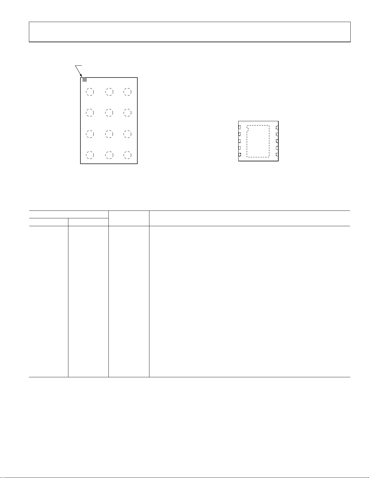
PIN CONFIGURATIONS AND FUNCTION DESCRIPTIONS
BALL A1
INDICATOR
1
PGND SGND VIN
A
23
SW
B
VOUT STROBE EN
C
LED_OUT SDA SCL
D
GPIO2
TOP VIEW
(BALL S IDE DOWN)
Not to Scale
GPIO1
1VIN
2GPIO2
ADP1650
3GPIO1
TOP VIEW
4SDA
5SCL
NOTES
1. THE EXPO SED PADDLE MUS T BE CONNECTED
08837-004
TO GRO UND.
10 STRO BE
9EN
8SW
7VOUT
6LED_OUT
08837-070
Figure 4. WLCSP Pin Configuration Figure 5. LFCSP Pin Configuration
Table 6. Pin Function Descriptions
Pin No.
WLCSP LFCSP Mnemonic Description
A1 N/A1 PGND Power Ground.
A2 N/A1 SGND Signal Ground.
A3 1 VIN Input Voltage for the Device. Connect an input bypass capacitor close to this pin.
B1 8 SW Boost Switch. Connect the power inductor between SW and the input capacitor.
B2 2 GPIO2
ILED/TX2/ADC. Mode is register selectable. Red indicator LED current source or
TxMASK2 or ADC input.
ILED Mode. Connect to red LED anode. Connect the LED cathode to power ground.
TxMASK2 Mode. Reduces the current to the programmable TxMASK2 current.
ADC Mode. This pin is used as the input pin for the ADC.
B3 3 GPIO1
Torch/TX1. Mode is register selectable. External torch mode or TxMASK1 input.
Torch Mode. Enables the integrated circuit (IC) in direct torch mode.
TxMASK1 Mode. Reduces the flash current to the programmable TxMASK1 current.
C1 7 VOUT
Boost Output. Connect an output bypass capacitor very close to this pin. This is the
output for the 5 V external voltage mode.
C2 10 STROBE
Strobe Signal Input. This pin synchronizes the flash pulse to the image capture. In
most cases, this signal comes directly from the image sensor.
C3 9 EN
Enable. Set EN low to bring the quiescent current (I
) to <1 μA. Registers are set to
Q
their defaults when EN is brought from low to high.
D1 6 LED_OUT LED Current Source. Connect this pin to the anode of the flash LED.
D2 4 SDA I2C Data Signal in I2C Mode.
D3 5 SCL I2C Clock Signal in I2C Mode.
0 EPAD Exposed Pad. Connect the exposed pad to the ground plane for the LFCSP version.
1
N/A means not applicable.
Rev. C | Page 7 of 32
Page 8
ADP1650
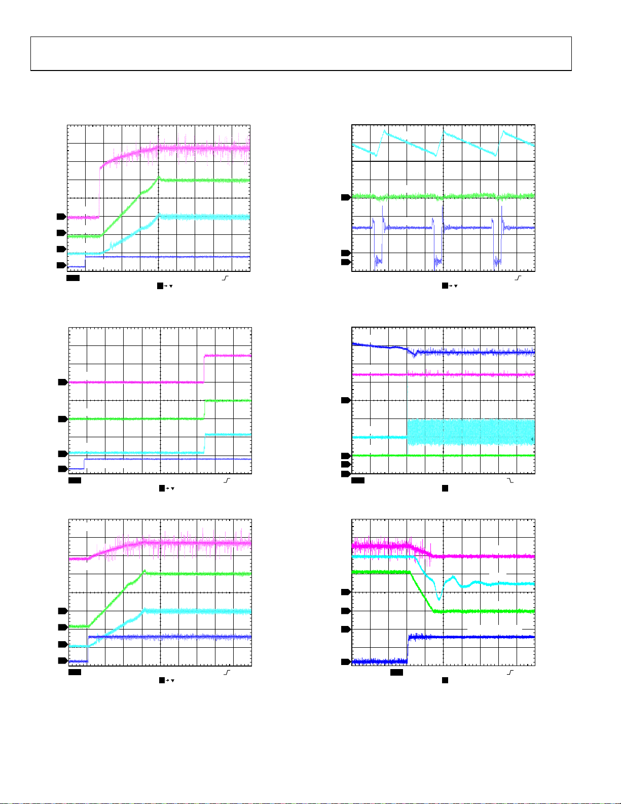
TYPICAL PERFORMANCE CHARACTERISTICS
IL = inductor current, I
LED_OUT
3
I
LED
4
I
L
2
STROBE
1
CH1 5V CH2 1A Ω
Figure 6. Startup Flash Mode, V
= LED current, LED_OUT = LED output, I
LED
CH4 500mA ΩCH3 1V
M100µs A CH1 400mV
T 402.2µs
= 3.6 V, I
IN
= 1500 mA
LED
= battery current.
BAT
I
L
I
4
2
1
08837-025
CH1 2V CH2 100m A Ω
Figure 9. Switching Waveforms, Flash Mode, I
VIN
LED
SW
CH4 25mA Ω
M100ns A CH1 1.6V
T 4.16007ms
= 1500 mA
LED
08837-031
LED_OUT
3
I
LED
4
I
L
2
GPIO1 (Torch)
1
CH1 5V CH2 100mA Ω
CH4 100mA ΩCH3 2V
Figure 7. Startup Torch Mode, V
VIN = 3.6V
LED_OUT
3
I
LED
4
I
L
2
STR
1
CH1 2V CH2 1A Ω
CH4 500mA ΩCH3 1V
M1.00ms A CH1 600mV
T 4.16ms
= 3.6 V, I
IN
M100µs A CH1 440mV
T 394.6µs
Figure 8. 100 mA Torch to 1500 mA Flash Transition
= 100 mA
LED
LED_OUT
3
I
L
I
LED
2
08837-026
08837-028
1
4
CH1 5V CH2 100m A Ω
CH4 100mA ΩCH3 2V
M1ms A CH2 88mA
T 30.40%
Figure 10. Pass-Through to Boost Mode Transition, I
LED_OUT
I
BAT
3
I
4
2
1
CH1 2V
CH2 1A Ω
CH4 500mA ΩCH3 1V
M10µs A CH1 680mV
T 30.60%
LED
GPIO1 (TxMASK1)
= 100 mA
LED
08837-032
08837-035
Figure 11. Entry into TxMASK1 Mode
Rev. C | Page 8 of 32
Page 9
ADP1650
C
C
100
LED_OUT
I
BAT
2
I
LED
3
4
GPIO1 ( TxMASK1)
1
CH2 2V
CH4
1A Ω M40µs A CH1 680mV
CH2
CH4 500mA Ω1V
T 16%
Figure 12. Exit from TxMASK1 Mode
08837-036
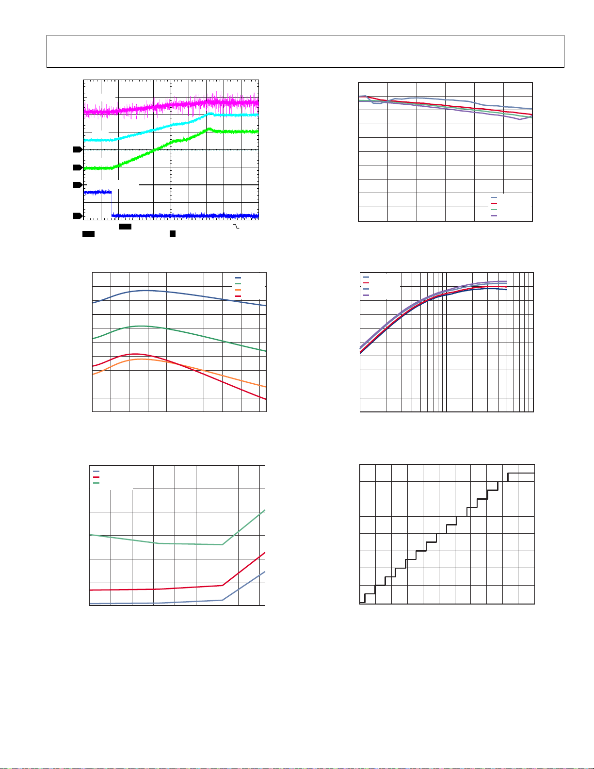
90
80
70
60
Y (%)
50
40
EFFICIEN
30
20
10
0
0.30.50.70.91.11.31.5
LED CURRENT (A)
VIN = 4.2V
V
= 3.6V
IN
V
= 3.4V
IN
V
= 3.2V
IN
Figure 15. Flash Mode Efficiency vs. LED Current
8837-044
3.04
3.03
3.02
3.01
3.00
2.99
(MHz)
SW
f
2.98
2.97
2.96
2.95
2.94
2.7 3.0 3.3 3.6 3.9 4.2 4. 5 4.8 5.1 5.4
INPUT VOLTAGE (V)
–40°C
+25°C
+85°C
+125°C
Figure 13. Switching Frequency vs. Supply Voltage (3 MHz Mode)
6
VIN = 2.7V
= 3.6V
V
IN
= 4.5V
V
IN
5
4
3
2
STANDBY CURRENT (µA)
1
100
VIN = 2.7V
= 3.0V
V
IN
90
80
70
60
Y (%)
50
40
EFFICIEN
30
20
10
08837-038
= 3.6V
V
IN
= 4.2V
V
IN
0
0.01 0. 1 1
OUTPUT CURRENT (A)
08837-045
Figure 16. Voltage Regulation Mode Efficiency vs. Load Current
1111
1110
1100
1010
1000
0110
ADC RESULT (Bin ary)
0100
0010
0
–40 –20 0 20 40 60 80 100 120
TEMPERATURE (°C)
Figure 14. Standby Current vs. Temperature
08837-043
0000
0 50 100 150 200 250 300 350 400 450 500 550
ADC INPUT VOLTAGE (mV)
Figure 17. ADC External Voltage Mode Transfer Characteristic
08837-059
Rev. C | Page 9 of 32
Page 10
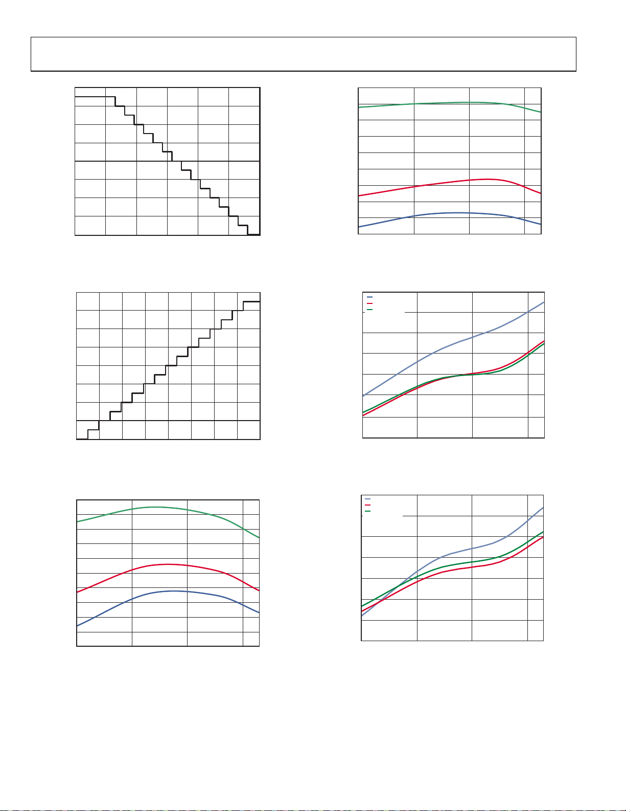
ADP1650
1111
1110
1100
1010
1000
0110
ADC RESULT (Binary)
0100
0010
0000
0 25 50 75 100 125 150
DIE TEMPERATURE (°C)
Figure 18. ADC Die Temperature Mode Transfer Characteristic
08837-060
295
294
293
292
291
290
289
CODE 1000 MIDPOINT (mV)
288
287
286
–40 10 60 110
= 5V
V
IN
V
= 3.6V
IN
V
= 2.7V
IN
TEMPERATURE (°C)
08837-063
Figure 21. ADC External Voltage Mode, Code 1000, Midpoint vs. Temperature
1111
1110
1100
1010
1000
0110
ADC RESULT (Bin ary)
0100
0010
0000
2.8 3.0 3. 2 3. 4 3. 6 3.8 4. 0 4. 2 4. 4
LED_OUT VOLTAGE (V)
Figure 19. ADC LED V
3.760
3.755
3.750
3.745
3.740
3.735
3.730
3.725
CODE 1000 MIDPO INT (V)
3.720
3.715
3.710
–40 10 60 110
Figure 20. ADC LED V
Mode Transfer Characteristic
F
V
= 5.0V
IN
V
IN
VIN = 2.7V
TEMPERATURE (°C)
Mode, Code 1000, Midpoint vs. Temperature
F
= 3.6V
1.0
VIN = 3.2V
V
= 3.6V
IN
V
= 4.2V
IN
0.5
0
–0.5
–1.0
–1.5
LED CURRENT ERROR (%)
LED CURRENT ERROR (%)
–2.0
–2.5
–40 10 60 110
8837-061
Figure 22. LED Current Accuracy vs. Temperature, I
0.5
VIN = 3.2V
V
= 3.6V
IN
V
= 4.2V
IN
0
–0.5
–1.0
–1.5
–2.0
LED CURRENT ERROR (%)
–2.5
–3.0
–40 10 60 110
08837-062
TEMPERATURE (°C)
TEMPERATURE (°C)
= 1200 mA
LED
08837-066
08837-067
Figure 23. LED Current Accuracy vs. Temperature, I
= 800 mA
LED
Rev. C | Page 10 of 32
Page 11

ADP1650
3.0
VIN = 3.2V
= 3.6V
V
IN
LED CURRENT ERRO R (%)
2.5
2.0
1.5
1.0
0.5
–0.5
–1.0
–1.5
–2.0
= 4.2V
V
IN
0
–40 10 60 110
TEMPERATURE (°C)
Figure 24. LED Current Error vs. Temperature, I
= 1500 mA
LED
08837-068
1.0
VIN = 3.2V
= 3.6V
V
IN
= 4.2V
V
IN
0.5
0
–0.5
–1.0
–1.5
LED CURRENT ERROR (%)
LED CURRENT ERROR (%)
–2.0
–2.5
–40 10 60 110
TEMPERATURE (°C)
Figure 25. LED Current Error vs. Temperature, I
= 1000 mA
LED
08837-069
Rev. C | Page 11 of 32
Page 12

ADP1650
V
THEORY OF OPERATION
The ADP1650 is a high power, I2C programmable white LED
driver ideal for driving white LEDs for use as a camera flash.
The ADP1650 includes a boost converter and a current
regulator suitable for powering one high power white LED.
WHITE LED DRIVER
The ADP1650 drives a synchronous 3 MHz boost converter as
required to power the high power LED. If the sum of the LED
forward voltage and current regulator voltage is higher than
the battery voltage, the boost turns on. If the battery voltage is
higher than the sum of the LED V
age, the boost is disabled and the part operates in pass-through
mode. The ADP1650 uses an integrated PFET high-side current
regulator for accurate brightness control.
and current regulator volt-
F
INPUT VOLTAGE =
VIN
L1
1µF
SW
2.7V TO 5. 0
PGND
C
IN
10µF
MODES OF OPERATION
Once the enable pin is high, the device can be set into the four
modes of operation using the LED_MOD bits in Register 0x04,
via the I
LED_MOD = [00] sets the device in standby mode, consuming
3 µA (typical).
LED_MOD = [01] sets the device in fixed VOUT = 5 V output
mode.
LED_MOD = [10] sets the device in assist light mode with
continuous LED current.
LED_MOD = [11] sets the device in flash mode with current up
to 1.5 A available for up to 1.6 sec.
2
C-compatible interface.
C
OUT
10µF
PGND
VOUT
HPLED
DRIVER
CURRENT
SENSE
HPLED
SHORT
HIGH POWER LED
CURRENT CONTROL
PGNDAGND
LED_OUT
25mA TO 1.5A
PGND
PGNDSGND
08837-006
SCL
SDA
STROBE
EN
2.4V
TORCH
IO1_CFG[5:4]
UVLO
PWM
CONTROLL ER
INTERFACE
AND
CONTROL
TXMASK1 TXMASK2
VIN
ILED
IO2_CFG[7:6]
GPIO1 GPIO2
CURRENT
SENSE
4-BIT
ADC
5.5V
OVP
REGISTER
IC THERMAL
SENSING
LED_OUT PIN
FAULT
Figure 26. Detailed Block Diagram
Rev. C | Page 12 of 32
Page 13

ADP1650
A
ASSIST LIGHT
The assist light provides continuous current programmable
from 25 mA to 200 mA. Set the assist light current using the
I_TOR bits (in Register 0x03). To enable assist, set LED_MOD
to assist light mode and set OUTPUT_EN = 1 (in Register 0x04).
Disable assist light mode by setting LED_MOD to standby
mode or setting OUTPUT_EN = 0.
I(ASSIST)
LED CURRENT
0A
I2C DATA BUS
REG 0x03, I_TOR = XXX mA
REG 0x04, OUTPUT _EN = 1
LED_MOD = 10
Figure 27. Enabling Assist Light Mode
REG 0x04, OUTPUT_EN = 0
FLASH MODE
Flash mode provides 300 mA to 1.5 A for a programmable time
of up to 1.6 seconds. Set the flash current using the I_FL bits (in
Register 0x03) and the maximum flash duration with the FL_TIM
bits (in Register 0x02). To enable flash mode, set LED_MOD
to flash mode and set OUTPUT_EN = 1. Enable flash without
STROBE by setting STR_MODE (in Register 0x04) to 0 (software
strobe). When STR_MODE is in hardware strobe mode, setting
the STROBE pin high enables flash and synchronizes it to the
image sensor. Hardware strobe mode has two modes for timeout:
level sensitive and edge sensitive.
I(FLASH)
LED CURR ENT
0A
STROBE
I(FLASH)
LED CURR ENT
I2C DATA BUS
0A
STROBE
REG 0x02, FL_TIM = XXXX ms
REG 0x03, I_FL = XXXXX mA
REG 0x04, OUT PUT_EN = 1
STR_LV = 0
LED_MOD = 11
FL_TIM
ADP1650 SETS OUTPUT_EN TO 0.
ADP1650 SETS LE D_MOD TO 00.
08837-009
Figure 29. Flash Operation: Edge-Sensitive Mode
In edge-sensitive mode, a positive edge on the STROBE pin
enables the flash, and the FL_TIM bits set the flash duration.
08837-007
ASSIST-TO-FLASH OPERATION
SH)
I(FL
LED CURRENT
I(ASSIST)
0A
STROBE
I2C D ATA BUS
REG 0x02, FL_T IM = XXXX ms
REG 0x03, I_TOR = XXX mA
REG 0x03, I_FL = XXXXX mA
REG 0x04, OUT PUT_EN = 1
LED_MOD = 10
Figure 30. Enabling Assist to Flash (Level-Sensitive) Mode
ADP1650 SETS OUT PUT_EN TO 0.
ADP1650 SETS LED_MOD TO 00.
STR_LV = 1
08837-010
The STR_POL bit in Register 0x07 changes the default enable of
STROBE from low to high to high to low. Additional image
sensor-specific assist/flash enable modes are included in the
device, and information on these is available on request from
the Analog Devices, Inc., sales team.
TORCH MODE
I2C DATA BUS
REG 0x02, FL _TIM = XXXX ms
REG 0x03, I_FL = XXXXX mA
REG 0x04, OUT PUT_EN = 1
LED_MOD = 11
STR_LV = 1
ADP1650 SETS OUTPUT_EN TO 0.
ADP1650 SETS LE D_MOD TO 00.
08837-008
Figure 28. Flash Operation: Level-Sensitive Mode
In level-sensitive mode, the duration of STROBE high sets the
duration of the flash up to the maximum time set by the
FL_TIM timeout. If STROBE is kept high longer than the
duration set by FL_TIM, a timeout fault disables the flash.
Rev. C | Page 13 of 32
Set the assist/torch light current using the I_TOR bits. To enable
torch mode using a logic signal, set LED_MOD to standby mode
and OUTPUT_EN = 1, and then bring GPIO1 high. Disable
external torch mode by setting GPIO1 low or programming
OUTPUT_EN = 0. Bringing GPIO1 low during torch mode
automatically sets OUTPUT_EN = 0. To enable torch mode
again, program OUTPUT_EN = 1, and bring GPIO high again.
I(ASSIST)
LED CURRENT
GPIO 1 (TORC H)
I2C DATA BUS
0A
REG 0x03, I_TO R = XXX mA
REG 0x04, OUTPUT _EN = 1
LED_MOD = 00
ADP1650 SETS OUTP UT_EN TO 0
Figure 31. Enabling External Torch Mode Using GPIO1
08837-065
Page 14

ADP1650
TORCH-TO-FLASH MODE
The driver can move directly from external torch mode (using
GPIO1) to flash mode by bringing STROBE high before GPIO1
= torch is brought low. Bringing torch low before STROBE goes
high prevents the flash from firing when STROBE goes high.
The ADP1650 returns to standby mode after a successful flash
and sets OUTPUT_EN = 0.
I(FLASH)
LED CURRENT
I(ASSIST)
0A
STROBE
TORCH
I2C D ATA BUS
REG 0x02, FL_TIM = XXXX ms
IO1_CFG = 01, TORCH
REG 0x03, I_T OR = XXX mA
REG 0x03, I _FL = XXX XX mA
REG 0x04, OUTPUT_EN = 1
LED_MOD = 00
Figure 32. Enabling Flash Mode from External Torch Mode
ADP1650 SETS OUTPUT_EN TO 0
STR_LV = 1
TxMASK OPERATION
When the ADP1650 is in flash mode, the TxMASK1 and
TxMASK2 functions reduce the battery load in response to the
system enabling a power amplifier. The device remains in flash
mode, but the LED driver output current reduces to the programmed TxMASK light level in less than 21 µs.
I(FLASH)
LED CURRENT
I(TXMASK1)
0A
TXMASK1
(GPIO1)
STROBE
08837-064
FREQUENCY FOLDBACK
Frequency foldback is an optional mode that optimizes
efficiency by reducing the switching frequency to 1.5 MHz
when VIN is slightly less than VOUT. Enable frequency
foldback by setting FREQ_FB = 1 in Register 0x04.
INDICATOR LED DRIVER
The indicator LED driver on GPIO2 provides a programmable
current source of between 2.75 mA and 11 mA for driving a red
privacy LED. The current level is programmed by the I_ILED
bits in Register 0x07. The circuit consists of a programmable
current source and a monitoring circuit that uses comparators
to determine whether the indicator LED is shorted or open. The
threshold for detection of a short is 1.2 V (maximum) and an
open circuit is 2.45 V (minimum). The indicator LED must not
be used at the same time as a flash or assist/torch event.
LOW BATTERY LED CURRENT FOLDBACK
As the battery discharges, the lower battery voltage results in
higher peak currents through the battery ESR, which may cause
early shutdown of the phone. The ADP1650 features an optional
low battery detection option, which reduces the flash current
(to a programmable level) when the battery voltage falls below a
programmable level.
VIN
50mV HY S
V(V_VB_LO)
STROBE
I2CDATABUS
REG 0x09 , I_VB_LO = XXXX mA
V_VB_LO = XXX V
REG 0x04, OUTPUT_EN = 1
LED_MOD = 10
Figure 34. Register 0x09 Sets the Battery Voltage Threshold Level and the
Reduced LED Current Level
GLITCH < 50µs IGNORED
FL_VB_LO = 1
ADP1650 SETS O UTPUT_EN TO 0.
ADP1650 SETS LE D_MOD TO 00.
08837-012
I2CDATABUS
REG 0x02 , IO 1_CFG = 10
FL_TIM = XXXX ms
REG 0x03, I_FL = XXXXX mA
REG 0x06, I_T X1 = XXXX mA
REG 0x04, OUT PUT_EN = 1
LED_MOD = 11
STR_LV = 1
FL_TX1 = 1
ADP1650 SETS OUT PUT_EN TO 0.
ADP1650 SETS LED_M OD TO 00.
Figure 33. TxMASK1 Operation During Flash (Level-Sensitive) Mode
The device selects the TxMASK1 or TxMASK2 current level
based on whether the TxMASK1 or TxMASK2 input is used.
After a TxMASK1 or TxMASK2 occurs, a flag is set in the fault
information register. When the TxMASK signal goes low again,
the LED current goes back to the full flash level in a controlled
manner to avoid overshoots on the battery current. If both
TxMASK inputs are set high simultaneously, the TXMASK1
current level is used.
Rev. C | Page 14 of 32
Table 7. VDD Level at Which the VBAT Low Function Is
Enabled
Bit Name VDD Level
V_VB_LO 000 = disabled (default)
001 = 3.3 V
010 = 3.35 V
8837-011
011 = 3.4 V
100 = 3.45 V
101 = 3.5 V
110 = 3.55 V
111 = 3.6 V
Set V_VB_LO = 000 to disable the low battery current foldback.
Page 15

ADP1650
PROGRAMMABLE BATTERY DC CURRENT LIMIT
The ADP1650 has four optional programmable input dc current
limits that limit the maximum battery current that can be taken
over all conditions. This allows higher LED currents to be used
in a system with significant variation in LED forward voltage
(V
) and supply battery voltage without risk of the current
F
allocated to the flash being exceeded.
ANALOG-TO-DIGITAL CONVERTER OPERATION
The internal 4-bit analog-to-digital converter (ADC) is configurable to measure the LED V
or an external voltage using the GPIO2 pin. Read the 4-bit
resolution output code back from Register 0x08 using the I
interface.
, integrated circuit (IC) die temperature,
F
2
C
Table 8. Input DC Current Limit Setting the LED Current
Bit Name Current Limit
IL_DC 00 = 1.5 A
01 = 1.75 A
10 = 2.0 A (default)
11 = 2.25 A
During startup of the flash, if the battery current does not reach
the dc current limit, the LED current is set to the current value
of the I_FL bits. If the battery current does hit the programmed
dc current limit on startup, the LED current does not increase
further. The dc current limit flag is set in the fault information
register. The I_FL bits in Register 0x03 are set to the actual LED
current and are available for readback.
NO LIM IT LED C URRENT
ACTUAL LED CURRENT
STROBE
I2C DATA BUS
REG 0x02, FL_TIM = XXXX ms
REG 0x03, I_FL = XXXXX mA
IL_DC_EN = 1
IL_DC = XX A
REG 0x04, OUTPUT_EN = 1
STR_LV = 1
LED_MOD = 11
Figure 35. DC Current Limit Operation in a Low Battery, High LED V
ADP1650 SETS OUTPUT_EN TO 0.
ADP1650 SETS LED_MOD TO 00.
ADP1650 SETS FL_IDC (REG 0x05) TO 1.
ADP1650 SETS I_FL TO ACTUAL LED CURRENT.
Case
F
08837-013
The camera system shown in Figure 36 can adjust the image
sensor settings based on the known reduced LED current for a
low battery and a high V
NO
LED CURRENT =
PROGAMMED LED
CURRENT
STROBE
LED.
F
SELECT FLASH CURRENT
SELECT MAX BATTE RY CURRENT
PREFLASH STROBE
DC LIMIT HIT?
YES
LED CURRENT =
REDUCED LED CURR ENT
BATTERY CURRE NT =
PROGRAMM ED DC LIMI T
I2C READ LED CURREN T
EN
IC TEMPERATURE
SDA
SCL
INTERFACE/
CONTROL
ADC_VAL[5:2]
SENSOR
ADC_EN[1:0]
4-BIT ADC
GPIO2
LED_OUT
PTC
Figure 37. Available ADC Modes in the ADP1650
The ADC can perform the conversion either immediately on an
2
I
C command, or it can delay the conversion until the next time
the ADP1650 exits an active mode. Delayed conversion can be
useful, for example, for measuring the IC temperature at the
end of a timed flash period. To set up a delayed conversion, set
ADC_EN to the required mode while OUTPUT_EN = 0. Then
set the ADP1650 to the desired output mode (torch, flash assist
light, or 5 V output) and set OUTPUT_EN = 1. The ADC conversion is performed when the ADP1650 exits the chosen mode.
To perform an immediate conversion, set ADC_EN to the
required mode during ADP1650 operation (OUTPUT_EN = 1).
Note that an ADC conversion cannot be performed when the
ADP1650 is idle. This is interpreted as an attempt to set up a
delayed conversion.
LED VF Mode
The ADC can measure the LED VF in both flash and assist/
torch modes. In torch mode, set ADC_EN = 01 to begin a
conversion. The value can be read back from the ADC_VAL[5:2]
bits 1 ms after the conversion has started. Assist/torch mode,
rather than flash mode, is best in the handset production test to
verify the LED V
START CONVE RSION
(INTERNAL S IGNAL)
.
F
1ms
08837-015
ADJUST IMAG E SENSO R
STROBE
Figure 36. Use of the DC Current Limit in an Optimized Camera System
08837-014
Figure 38. ADC Timing for All Modes Except V
In flash mode, set ADC_EN = 01. The conversion happens just
before the timeout occurs; therefore, the FL_TIM bits set when
the ADC sample occurs. This allows the V
Rev. C | Page 15 of 32
2
I
C DATA BUS
REG 0x08, ADC_EN = 01
ADC_VAL[5:2]
AVAILABLE F OR READ
Measurement in Flash Mode
F
to settle from the
F
08837-016
Page 16

ADP1650
=
V
initial peak as the junction temperature of the LED stabilizes.
An LED temperature vs. flash time profile for the handset PCB
design can be generated during the design phase by varying the
FL_TIM bits from the lowest to the highest setting and collecting a
V
sample on each flash.
F
I(FLASH)
LED CURRENT
START CO NVERSIO N
(INTERNAL SIGNAL)
I2C DATA BUS
0A
STROBE
REG 0x02, FL_TIM = XX XX ms
REG 0x03, I_FL = XXXXX mA
REG 0x04, O UTPUT _EN = 1
STR_LV = 0
LED_MOD = 11
Figure 39. ADC Timing for V
FL_TIM
ADC_VAL[5:2]
AVAILABL E FOR READ
REG 0x08, AD C_EN = 01
Measurement in Flash Mode
F
t
S
= 1ms
Die Temperature Mode
The ADC measures the IC die temperature and provides the
2
result to the I
C interface. This is useful during the design phase
of the flash system to optimize PCB layout for the best thermal
design.
08837-017
Write ADC_EN = 10 to begin a die temperature measurement.
The value can be read back from the ADC_VAL[5:2] bits 1 ms
after the conversion has started. The most stable and accurate
value of die temperature is available at the end of the flash pulse.
External Voltage Mode
The ADC measures the voltage on the GPIO2 pin when the
GPIO2 is configured as an ADC input by setting IO2_CFG =
11. One example is using an external temperature-dependent
resistor to create a voltage based on the temperature of the flash
LED. The EN line can be used for biasing to reduce leakage
current when the flash is not being used.
5 V OUTPUT OPERATION
The ADP1650 can be used as a 5 V boost to supply up to 500 mA
for an audio voltage rail or keypad LED driver voltage. To move
into voltage regulation mode, the OUTPUT_EN bit must be set
to 0. To enable the 5 V output, set LED_MOD[1:0] = 01, and set
OUTPUT_EN = 1. The ADP1650 sets the VOUT pin to 5 V
and disconnects VOUT from LED_OUT. The VOUT pin is
connected to the SW node when the ADP1650 is not enabled.
VOUT should not be connected directly to a positive external
voltage source because this causes current to flow from VOUT
to the battery.
2.7V TO 5. 0
10µF
VOUT = 5.0V
10µF
VDD
KEYPAD
LED DRIV ER
GND
VIN
SGND
INPUT VOLTAGE
1.0µH
SWSTROBE
VOUT*
LED_OUT
PGND
ON
3.2 MEGAPIXEL
TO 5.0 MEGAPIXE L
CMOS IMAGE SENSOR
APPLICATIONS PROCESSOR
SDA, SCL
EN
*THE VOUT P IN IS CONNECT ED TO T HE SW NODE W HEN THE ADP1650 I S NOT ENABLED. VOUT S HOULD NOT BE CONNECTED DI RECTLY T O A POSITIVE
EXTERNAL VO LTAGE S OURCE BECAUSE THI S WILL CAUSE CURRENT TO FLOW FROM VOUT TO THE BATTERY.
OFF
2
I
C BUS
POWER-ON RESET
GPIO2
SCL
SDA
EN
GPIO1
ADP1650
Figure 40. ADP1650 Voltage Regulation Mode: LED Driver Application
08837-018
Rev. C | Page 16 of 32
Page 17

ADP1650
V
3.2 TO 5.0 MEGAPIXEL
CMOS IMAGE SENSOR
APPLICATIONS PROCESSOR
SDA, SCL
EN
ON
OFF
I2C BUS
POWER-ON
RESET
2.7V TO 5.0
10µF
VOUT = 5. 0V ±8.5%, IMAX = 500mA
10µF
0.1µF
AUDIO IN+
AUDIO IN–
SHUTDOWN
47nF
47nF
VDD
IN+
IN–
SD
80kΩ
80kΩ
GPIO2
SCL
SDA
EN
GPIO1
VIN
ADP1650
SGND
INPUT VOLTAGE =
1.0µH
SWSTROBE
VOUT
LED_OUT
PGND
Figure 41. ADP1650 Voltage Regulation Mode: Class-D Audio Application
160kΩ
MODULATOR
(Σ-∆)
160kΩ
INTERNAL
BIAS
OSCILLATOR
FET
DRIVER
GND
SSM2315
OUT+
OUT–
POP/CLICK
SUPPRESSION
08837-019
Rev. C | Page 17 of 32
Page 18

ADP1650
SAFETY FEATURES
For critical fault conditions, such as output overvoltage, flash
timeout, LED output short circuit, and overtemperature
conditions, the ADP1650 has built-in protection modes. If a
critical fault occurs, OUTPUT_EN (Register 0x04) is set to 0,
and the driver shuts down. The appropriate fault bit is set in the
fault information register (Register 0x05). The processor can
read the fault information register through the I
determine the nature of the fault condition. When the fault
register is read, the corresponding fault bit is cleared.
If a noncritical event such as an indicator LED open/short or a
TxMASK1 or TxMASK2 event occurs, or the dc current limit or
soft inductor current limit is hit, the LED driver continues
operating. The corresponding information bits are set in the
fault information register until the processor reads them.
2
C interface to
SHORT-CIRCUIT FAULT
When the flash driver is disabled, the high-side current regulator
disconnects the dc path between the battery and the LED, protecting the system from an LED short circuit. The LED_OUT
pin features short-circuit protection that monitors the LED
voltage when the LED driver is enabled. If the LED_OUT pin
remains below the short-circuit detection threshold, a short
circuit is detected. Bit 6 of the fault information register is set
high. The ADP1650 remains disabled until the processor clears
the fault register.
OVERVOLTAGE FAULT
The ADP1650 contains a comparator at the VOUT pin that
monitors the voltage between VOUT and GND. If the voltage
exceeds 5.5 V (typical), the ADP1650 shuts down. Bit 7 in the
fault information register is read back as high. The ADP1650 is
disabled until the fault is cleared, ensuring protection against an
open circuit.
DYNAMIC OVERVOLTAGE MODE (DOVP)
Dynamic OVP mode is a programmable feature that limits the
VOUT voltage exceeding the OVP level while maintaining as
much current as possible through the LED. This mode prevents
an overvoltage fault in the case of a much higher than expected
LED forward voltage. If the LED forward voltage reduces due to
the LED temperature rising, the ADP1650 moves out of DOVP
mode and regulates the LED at the programmed current level.
Set Bit 7 of Register 0x07 high to enable dynamic OVP mode.
TIMEOUT FAULT
When external strobe mode is enabled (Register 0x04, Bit 2),
and strobe is set to level-sensitive mode (Register 0x04, Bit 5),
if the strobe pin remains high for longer than the programmed
timeout period, the timeout fault bit (Register 0x05, Bit 4) is
read back as high. The ADP1650 remains disabled until the
processor clears the fault register.
OVERTEMPERATURE FAULT
If the junction temperature of the ADP1650 rises above 150°C,
a thermal protection circuit shuts down the device. Bit 5 of the
fault information register is set high. The ADP1650 remains
disabled until the processor clears the fault register.
INDICATOR LED FAULT
The GPIO2 pin features open- and short-circuit protection in
the indicator LED mode. If a short or open circuit occurs, Bit 2
of the fault information register is set high. The indicator LED
regulator ensures that no damage occurs to the IC during a fault.
CURRENT LIMIT
The internal switch limits battery current by ensuring that the
peak inductor current does not exceed the programmed limit
(current limit is set by Bit 6 and Bit 7 in Register 0x04). The
default mode of the ADP1650 is soft current limit mode. If the
peak inductor current hits the limit, Bit 1 of the fault information register is set, and the inductor and LED current cannot
increase further. The ADP1650 continues to operate. If the
ADP1650 has soft current limit disabled and the peak inductor
current exceeds the limit, the part shuts down and Bit 1 of the
fault information register is set high. In this case, ADP1650
remains disabled until the processor clears the fault register.
INPUT UNDERVOLTAGE
The ADP1650 includes a battery undervoltage lockout circuit.
During 5 V or LED operation, if the battery voltage drops below
the 2.4 V (typical) input UVLO threshold, the ADP1650 shuts
down. A power-on reset circuit resets the registers to their
default conditions when the voltage rises above the UVLO
rising threshold.
SOFT START
The ADP1650 has a soft start mode that controls the rate of
increase of battery current at startup by digitally controlling the
output current ramp. The maximum soft start time is 0.6 ms.
RESET USING THE ENABLE (EN) PIN
A low-to-high transition on the EN pin resets all registers to
their default values. Bringing EN low reduces the I
(typical).
to 0.2 µA
Q
CLEARING FAULTS
The information bits and faults in Register 0x05 clear
automatically when the processor reads the fault register.
Rev. C | Page 18 of 32
Page 19

ADP1650
I2C INTERFACE
The ADP1650 includes an I2C-compatible serial interface for
control of the LED current, as well as for readback of system
status registers. The I
mode and 0x61 in read mode). Additional I
available on request.
2
C chip address is 0x30 (0x60 in write
S
01 100 00 0
T
2
C addresses are
CHIP ADDRESS
0 = WRITE
0
DP1650 ACK
Figure 42. I
0 = WRITE 1 = READ
S
011000 0 0
T
CHIP ADDRESS
SUBADDRESS
Figure 42 illustrates the I
The subaddress content selects which of the nine ADP1650
registers is written to. The ADP1650 sends an acknowledgment
to the master after the 8-bit data byte has been written. Figure 43
shows the I
The register definitions are shown in the I
section.
00
SUBADDRESS
2
C Single Register Write Sequence
S
0
0110000 01 0
T
CHIP ADDRESS
ADP1650 RECEIVES
ADP1650 ACK
2
C write sequence to a single register.
2
C read sequence of a single register.
2
C Register Map
MASTER
STOP
S
P
DATA
ADP1650 ACK
AD P1650 SEN DS
DATA
08837-021
MASTER
STOP
S
10
P
ADP1650 ACK
Figure 43. I
ADP1650 ACK
2
C Single Register Read Sequence
ADP1650 ACK
MASTER ACK
08837-020
Rev. C | Page 19 of 32
Page 20

ADP1650
I2C REGISTER MAP
The lowest bit number (0) represents the least significant bit, and the highest bit number (7) represents the most significant bit.
Table 9. Design Information Register (Register 0x00)
Bit R/W Reset State
[7:0] R 00100010
Table 10. VREF and Timer Register (Register 0x02)
Bit Name Bit R/W Description
IO2_CFG [7:6] R/W
IO1_CFG [5:4] R/W
FL_TIM [3:0] R/W Flash timer value setting
GPIO2 configuration
00 = high impedance (default)
01 = indicator LED
10 = TxMASK2 operation mode
11 = analog input (to ADC)
GPIO1 configuration
00 = high impedance (default)
01 = torch
10 = TxMASK1 operation mode
11 = reserved
0000 = 100 ms
0001 = 200 ms
0010 = 300 ms
0011 = 400 ms
0100 = 500 ms
0101 = 600 ms
0110 = 700 ms
0111 = 800 ms
1000 = 900 ms
1001 = 1000 ms
1010 = 1100 ms
1011 = 1200 ms
1100 = 1300 ms
1101 = 1400 ms
1110 = 1500 ms
1111 = 1600 ms (default)
Rev. C | Page 20 of 32
Page 21

ADP1650
Table 11. Current Set Register (Register 0x03)
Bit Name Bit R/W Description
I_FL [7:3] R/W Flash current value setting
00000 = 300 mA
00001 = 350 mA
00010 = 400 mA
00011 = 450 mA
00100 = 500 mA
00101 = 550 mA
00110 = 600 mA
00111 = 650 mA
01000 = 700 mA
01001 = 750 mA
01010 = 800 mA
01011 = 850 mA
01100 = 900 mA
01101 = 950 mA
01110 = 1000 mA (default)
01111 = 1050 mA
10000 = 1100 mA
10001 = 1150 mA
10010 = 1200 mA
10011 = 1250 mA
10100 = 1300 mA
10101 = 1350 mA
10110 = 1400 mA
10111 = 1450 mA
11000 = 1500 mA
I_TOR [2:0] R/W Torch and assist light current value setting
000 = 25 mA
001 = 50 mA
010 = 75 mA
011 = 100 mA (default)
100 = 125 mA
101 = 150 mA
110 = 175 mA
111 = 200 mA
Rev. C | Page 21 of 32
Page 22

ADP1650
Table 12. Output Mode Register (Register 0x04)
Bit Name Bit R/W Description
IL_PEAK [7:6] R/W Inductor peak current limit setting
00 = 1.75 A
01 = 2.25 A
10 = 2.75 A (default)
11 = 3.0 A
STR_LV 5 R/W 0 = edge sensitive
1 = level sensitive (default)
FREQ_FB 4 R/W 0 = frequency foldback to 1.5 MHz not allowed (default)
1 = frequency foldback to 1.5 MHz allowed
OUTPUT_EN 3 R/W 0 = output off (default)
1 = output on
STR_MODE 2 R/W 0 = software strobe mode (software flash occurs when output is enabled in flash mode)
1 = hardware strobe mode (the STROBE pin must go high for flash) (default)
LED_MOD [1:0] R/W Configures LED output mode
00 = standby mode (default)
01 = voltage output mode, VOUT = 5 V
10 = assist light mode
11 = flash mode
Table 13. Fault Information Register (Register 0x05)
Bit Name Bit R/W Description
FL_OVP 7 R 0 = no fault (default)
1 = overvoltage fault
FL_SC 6 R 0 = no fault (default)
1 = short-circuit fault
FL_OT 5 R 0 = no fault (default)
1 = overtemperature fault
FL_TO 4 R 0 = no fault (default)
1 = timeout fault
FL_TX1 3 R 0 = no TxMASK1 operation mode during last flash (default)
1 = TxMASK1 operational mode occurred during last flash
FL_IO2 2 R If GPIO2 is configured as TxMASK2
0 = no TxMASK2 operations mode during last flash (default)
1 = TxMASK2 operational mode occurred during last flash
If GPIO2 is configured as ILED
0 = no fault (default)
1 = indicator LED fault
FL_IL 1 R 0 = no fault (default)
1 = inductor peak current limit fault
FL_IDC 0 R 0 = programmed dc current limit not hit (default)
1 = programmed dc current limit hit
Rev. C | Page 22 of 32
Page 23

ADP1650
Table 14. Input Control Register (Register 0x06)
Bit Name Bit R/W Description
I_TX2 [7:4] R/W TxMASK2 operational mode foldback current
0000 = 100 mA
0001 = 150 mA
0010 = 200 mA
0011 = 250 mA
0100 = 300 mA
0101 = 350 mA
0110 = 400 mA (default)
0111 = 450 mA
1000 = 500 mA
1001 = 550 mA
1010 = 600 mA
1011 = 650 mA
1100 = 700 mA
1101 = 750 mA
1110 = 800 mA
1111 = 850 mA
I_TX1 [3:0] R/W TxMASK1 operational mode foldback current
0000 = 100 mA
0001 = 150 mA
0010 = 200 mA
0011 = 250 mA
0100 = 300 mA
0101 = 350 mA
0110 = 400 mA (default)
0111 = 450 mA
1000 = 500 mA
1001 = 550 mA
1010 = 600 mA
1011 = 650 mA
1100 = 700 mA
1101 = 750 mA
1110 = 800 mA
1111 = 850 mA
Rev. C | Page 23 of 32
Page 24

ADP1650
Table 15. Additional Mode Register, AD_MOD (Register 0x07)
Bit Name Bit R/W Description
DYN_OVP 7 R/W Dynamic OVP
0 = dynamic OVP off (default)
1 = dynamic OVP on
SW_LO 6 R/W Force 1.5 MHz switching frequency
0 = disabled (default)
1 = enabled
STR_POL 5 R/W Strobe polarity
0 = active low
1 = active high (default)
I_ILED [4:3] R/W Indicator LED current
00 = 2.75 mA (default)
01 = 5.5 mA
10 = 8.25 mA
11 = 11 mA
IL_DC [2:1] R/W Input dc current limit setting LED current
00 = 1.5 A
01 = 1.75 A
10 = 2.0 A (default)
11 = 2.25 A
IL_DC_EN 0 R/W Input dc current limit
0 = disabled (default)
1 = enabled
Table 16. Additional Mode Register, ADC (Register 0x08)
Bit Name Bit R/W Description
Reserved 7 R/W Test mode
0 = disabled (default)
1 = enabled
FL_VB_LO 6 R Programmed VBAT low threshold status; low battery mode must be enabled in Register 0x09
0 = VDD is greater than the VBAT low threshold (default)
1 = VDD is less than the VBAT low threshold
ADC_VAL [5:2] R/W ADC readback value; four bits (see Figure 17, Figure 18, and Figure 19)
ADC_EN [1:0] R/W ADC enable mode
00 = disabled (default)
01 = LED V
10 = die temperature measurement
11 = external voltage mode
measurement
F
Rev. C | Page 24 of 32
Page 25

ADP1650
Table 17. Battery Low Mode Register (Register 0x09)
Bit Name Bit R/W Description
CL_SOFT 7 R/W Soft inductor peak current limit
0 = disabled (ADP1650 is disabled when the inductor peak current limit is hit)
1 = enabled (default)
I_VB_LO [6:3] R Current setting for VBAT low mode
0000 = 300 mA
0001 = 350 mA
0010 = 400 mA
0011 = 450 mA
0100 = 500 mA
0101 = 550 mA
0110 = 600 mA
0111 = 650 mA
1000 = 700 mA
1001 = 750 mA
1010 = 800 mA (default)
1011 = 850 mA
1100 = 900 mA
1101 = 950 mA
1110 = 1000 mA
1111 = 1050 mA
V_VB_LO [2:0] R/W VDD level where VBAT low function is enabled
000 = disabled (default)
001 = 3.3 V
010 = 3.35 V
011 = 3.4 V
100 = 3.45 V
101 = 3.5 V
110 = 3.55 V
111 = 3.6 V
Rev. C | Page 25 of 32
Page 26

ADP1650
APPLICATIONS INFORMATION
EXTERNAL COMPONENT SELECTION
Selecting the Inductor
The ADP1650 boost converter increases the battery voltage
to allow driving of one LED, whose voltage drop is higher than
the battery voltage plus the current source headroom voltage.
This allows the converter to regulate the LED current over the
entire battery voltage range and with a wide variation of LED
forward voltage.
The inductor saturation current should be greater than the sum
of the dc input current and half the inductor ripple current. A
reduction in the effective inductance due to saturation increases
the inductor current ripple. Tab le 1 8 provides a list of recommended inductors.
Selecting the Input Capacitor
The ADP1650 requires an input bypass capacitor to supply
transient currents while maintaining constant input and output
voltages. The input capacitor carries the input ripple current,
allowing the input power source to supply only the dc current.
Increased input capacitance reduces the amplitude of the
switching frequency ripple on the battery. Due to the dc bias
characteristics of ceramic capacitors, a 0603, 6.3 V, X5R/X7R,
10 µF ceramic capacitor is preferable.
Higher value input capacitors help to reduce the input voltage
ripple and improve transient response.
To minimize supply noise, place the input capacitor as close to
the VIN pin of the ADP1650 as possible. As with the output
capacitor, a low ESR capacitor is required. Tab le 1 9 provides a
list of suggested input capacitors.
Selecting the Output Capacitor
The output capacitor maintains the output voltage and supplies
the LED current during the NFET power switch on period. It also
stabilizes the loop. The recommended capacitor is a 10 µF, 6.3 V,
X5R/X7R ceramic capacitor.
Note that dc bias characterization data is available from capacitor manufacturers and should be taken into account when
selecting input and output capacitors. The 6.3 V capacitors are
best for most designs. Tabl e 20 provides a list of recommended
output capacitors.
Higher output capacitor values reduce the output voltage ripple
and improve load transient response. When choosing this value,
it is also important to account for the loss of capacitance due to
output voltage dc bias.
Ceramic capacitors have a variety of dielectrics, each with different
behavior over temperature and applied voltage. Capacitors must
have a dielectric that ensures the minimum capacitance over the
necessary temperature range and dc bias conditions. X5R or X7R
dielectrics with a voltage rating of 6.3 V or 10 V are recommended
for best performance. Y5V and Z5U dielectrics are not recommended for use with any dc-to-dc converter because of their
poor temperature and dc bias characteristics.
Table 18. Suggested Inductors
Vendor Value (µH) Part No. DCR (mΩ) ISAT (A) Dimensions L × W × H (mm)
Toko 1.0 FDSD0312 41.5 4.5 3.0 × 3.0 × 1.2
Toko 1.0 DFE2520 50 3.4 2.5 × 2.0 × 1.2
Coilcraft 1.0 XFL3010 43 2.4 3.0 × 3.0 × 1.0
Murata 1.0 LQM32P_G0 60 3 3.2 × 2.5 × 1.0
FDK 1.0 MIPS3226D 40 3 2.5 × 2.0 × 1.2
Table 19. Suggested Input Capacitors
Vendor Value Part No. Dimensions L × W × H (mm)
Murata 10 μF, 6.3 V GRM188R60J106ME47 1.6 × 0.8 × 0.8
TDK 10 μF, 6.3 V C1608JB0J106K 1.6 × 0.8 × 0.8
Taiyo Yuden 10 μF, 6.3 V JMK107BJ106MA 1.6 × 0.8 × 0.8
Table 20. Suggested Output Capacitors
Vendor Value Part No. Dimensions L × W × H (mm)
Murata 10 μF, 6.3 V GRM188R60J106ME47 1.6 × 0.8 × 0.8
TDK 10 μF, 6.3 V C1608JB0J106K 1.6 × 0.8 × 0.8
Taiyo Yuden 10 μF, 6.3 V JMK107BJ106MA 1.6 × 0.8 × 0.8
Rev. C | Page 26 of 32
Page 27

ADP1650
A
The worst-case capacitance accounting for capacitor variation
over temperature, component tolerance, and voltage is calculated using the following equation:
C
= C
EFF
× (1 − TEMPCO) × (1 − TOL)
OUT
where:
C
is the effective capacitance at the operating voltage.
EFF
TEMPCO is the worst-case capacitor temperature coefficient.
TOL is the worst-case component tolerance.
In this example, the 10 F X5R capacitor has the following
characteristics:
TEMPCO from −40°C to +85°C is 15%.
TOL is 10%.
C
at VOUT (MAX) = 5 V, is 3 F, as shown in Figure 44.
OUT
10
0
–10
–20
–30
–40
–50
–60
PACITANCE CHANGE (%)
C
–70
–80
–90
1.260
DC BIAS VOLTAGE (V)
6.305.043.782.52
Figure 44. DC Bias Characteristic of a 3 × 6.3 V, 10 μF Ceramic Capacitor
Substituting these values in the equation yields
= 3 F × (1 − 0.15) × (1 − 0.1) = 2.29 F
C
EFF
The effective capacitance needed for stability, which includes
temperature and dc bias effects, is 3.0 F.
08837-022
Rev. C | Page 27 of 32
Page 28

ADP1650
A
PCB LAYOUT
Poor layout can affect performance, causing electromagnetic
interference (EMI) and electromagnetic compatibility (EMC)
problems, ground bounce, and power losses. Poor layout can
also affect regulation and stability. Figure 45 shows optimized
layouts implemented using the following guidelines:
• Place the inductor, input capacitor, and output capacitor
close to the IC using short tracks. These components carry
high switching frequencies and large currents.
• Route the trace from the inductor to the SW pin with as
wide a trace as possible. The easiest path is through the
center of the output capacitor.
• Route the LED_OUT path away from the inductor and SW
node to minimize noise and magnetic interference.
Li-ION +
• Maximize the size of ground metal on the component side
to help with thermal dissipation.
• Use a ground plane with two to three vias connecting to the
component side ground near the output capacitor to
reduce noise interference on sensitive circuit nodes.
• With the LFCSP package, six to eight thermal vias connect
the ground paddle to the main PCB ground plane.
• Analog Devices applications engineers can be contacted
through the Analog Devices sales team to discuss different
layouts based on system design constraints.
1
C
L1
INDUCTOR
AREA = 16.4mm
2
C2
PGND
LED
ANODE
Li-ION +
DIGIT AL
INPUT/
OUTPUT
8837-023
Figure 45. Layout of the ADP1650 Driving a High Power White LED (WLCSP)
Li-ION +
C1
VIN
GPIO2
O
PI
G
SDA
SCL
PGND
STROBE
EN
1
GND
SW
VOUT
LED_OUT
L1
INDUCTOR
C2
VOUT
DP1650
PGND
08837-024
Figure 46. Example Layout of the ADP1650 Driving a High Power White LED (LFCSP)
Rev. C | Page 28 of 32
Page 29

ADP1650
OUTLINE DIMENSIONS
0.660
0.602
0.544
SEATING
PLANE
0.330
0.310
0.290
1.50
REF
3
2
1
A
B
C
BALL A1
IDENTIFIER
1.54
1.50
1.46
2.04
2.00
1.96
0.022
REF
TOP VIE W
(BALL SIDE DOWN)
PIN 1 INDEX
AREA
0.80
0.75
0.70
SEATING
PLANE
0.50
0.380
0.352
0.324
0.04 MAX
COPLANARITY
0.280
0.250
0.220
REF
Figure 47. 12-Ball Wafer Level Chip Scale Package [WLCSP]
(CB-12-4)
Dimensions shown in millimeters
2.48
3.10
3.00 SQ
2.90
TOP VIEW
0.30
0.25
0.20
0.50
0.40
0.30
0.05 MAX
0.02 NOM
0.20 REF
2.38
2.23
6
EXPOSED
PAD
5
BOTTOM VIEW
FOR PROPER CONNECTION OF
THE EXPOSED PAD, REFER TO
THE PIN CONFIGURATION AND
FUNCTION DESCRIPTIONS
SECTION OF THIS DATA SHEET.
0.50 BSC
10
1
Figure 48. 10-Lead Lead Frame Chip Scale Package [LFCSP_WD]
3 mm × 3 mm Body, Very Very Thin, Dual Lead
(CP-10-9)
Dimensions shown in millimeters
1.00
REF
P
I
(
N
R
1.74
1.64
1.49
N
I
D
1
I
.
0
BOTTOM VIEW
(BALLSIDE UP)
A
R
O
T
C
)
5
1
121009-A
D
020409-B
ORDERING GUIDE
Model1 Temperature Range Package Description Package Option2 Branding
ADP1650ACBZ-R7 −40°C to +125°C 12-Ball Wafer Level Chip Scale Package [WLCSP] CB-12-4 LE4
ADP1650ACPZ-R7 −40°C to +125°C 10-Lead Frame Chip Scale Package [LFCSP_WD] CP-10-9 LGX
ADP1650CB-EVALZ Evaluation Board WLCSP Package
ADP1650CP-EVALZ Evaluation Board LFCSP Package
1
Z = RoHS Compliant Part.
2
This package option is halide free.
Rev. C | Page 29 of 32
Page 30

ADP1650
NOTES
Rev. C | Page 30 of 32
Page 31

ADP1650
NOTES
Rev. C | Page 31 of 32
Page 32

ADP1650
NOTES
©2010–2011 Analog Devices, Inc. All rights reserved. Trademarks and
registered trademarks are the property of their respective owners.
D08837-0-4/11(C)
Rev. C | Page 32 of 32
 Loading...