

Page 1
CMOS Linear Regulator
ADP151
Rev. E
Information furnished by Analog Devices is believed to be accurate and reliable. However, no
Trademarks and registered trademarks are the property of their respective owners.
Fax: 781.461.3113 ©2010–2012 Analog Devices, Inc. All rights reserved.
NC = NO CONNECT
1
2
3
5
4
1µF
1µF
V
OUT
= 1.8VV
IN
= 2.3V
VOUT
NC
VIN
GND
EN
OFF
ON
08627-001
VIN VOUT
1 2
EN GND
C
OUT
1µF
C
IN
V
OUT
= 1.8V
V
IN
= 2.3V
TOP VIEW
(Not to Scale)
A
B
OFF
ON
08627-002
ADP151
TOP VIEW
(Not to Scale)
4
6
5
GND
VOUT
NC
3
1
2
EN
VIN
NC
08627-047
NC = NO CONNECT. DO NOT
CONNECT TO THIS PIN.
ON
OFF
1µF 1µF
V
IN
= 2.3V V
OUT
= 1.8V
Data Sheet
FEATURES
Ultralow noise: 9 µV rms
No noise bypass capacitor required
Stable with 1 µF ceramic input and output capacitors
Maximum output current: 200 mA
Input voltage range: 2.2 V to 5.5 V
Low quiescent current
I
= 10 µA with 0 load
GND
I
= 265 μA with 200 mA load
GND
Low shutdown current: <1 µA
Low dropout voltage: 140 mV at 200 mA load
Initial accuracy: ±1%
Accuracy over line, load, and temperature: ±2.5%
16 fixed output voltage options: 1.1 V to 3.3 V
PSRR performance of 70 dB at 10 kHz
Current-limit and thermal overload protection
Logic controlled enable
Internal pull-down resistor on EN input
5-lead TSOT package
6-lead LFCSP package
4-ball, 0.4 mm pitch WLCSP
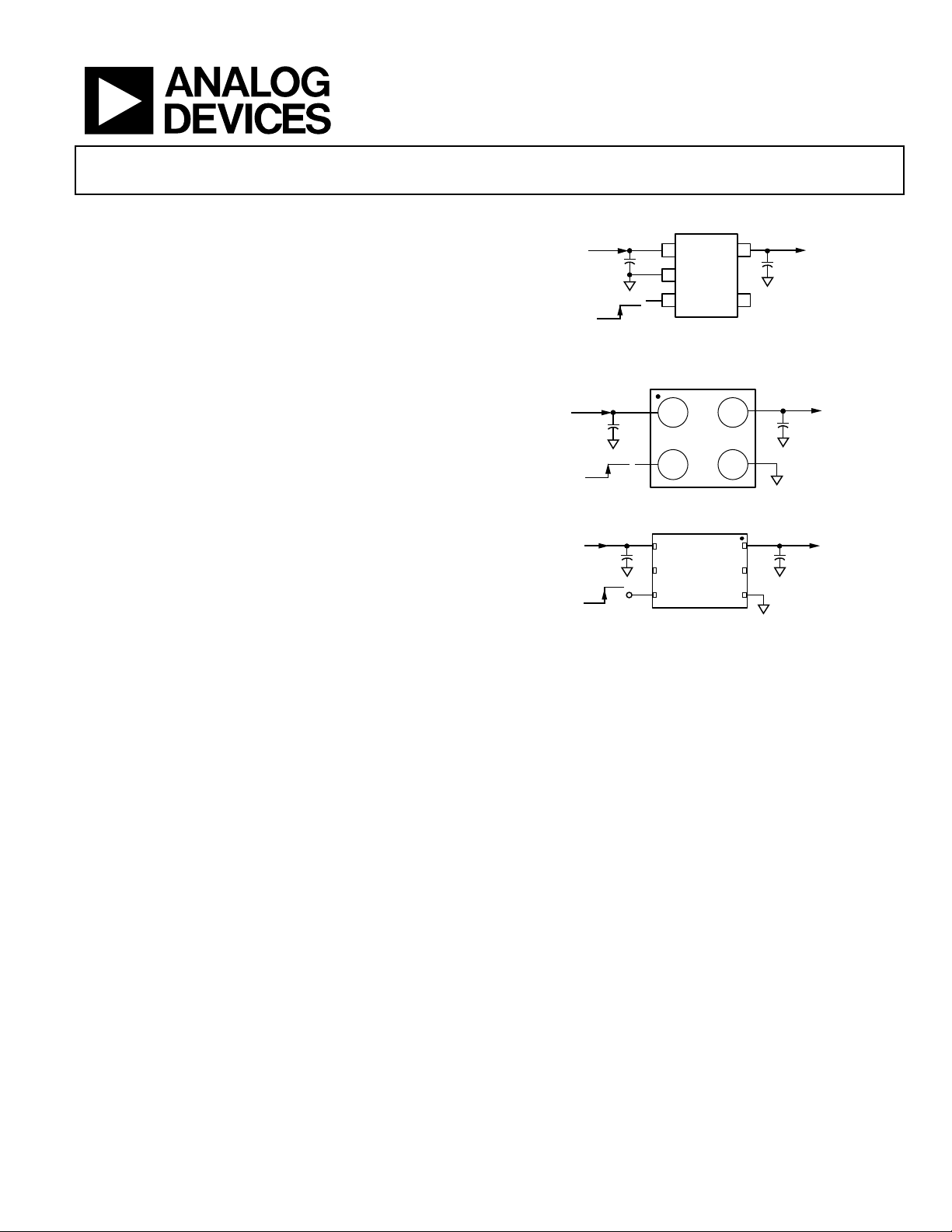
Ultralow Noise, 200 mA,
TYPICAL APPLICATION CIRCUIT
Figure 1. TSOT ADP151 with Fixed Output Voltage, 1.8 V
Figure 2. WLCSP ADP151 with Fixed Output Voltage, 1.8 V
APPLICATIONS
RF, VCO, and PLL power supplies
Mobile phones
Digital camera and audio devices
Portable and battery-powered equipment
Post dc-to-dc regulation
Portable medical devices
GENERAL DESCRIPTION
The ADP151 is an ultralow noise, low dropout linear regulator
that operates from 2.2 V to 5.5 V and provides up to 200 mA
of output current. The low 140 mV dropout voltage at 200 mA
load improves efficiency and allows operation over a wide input
voltage range.
Using an innovative circuit topology, the ADP151 achieves
ultralow noise performance without the necessity of a bypass
capacitor, making it ideal for noise-sensitive analog and RF
applications. The ADP151 also achieves ultralow noise performance without compromising PSRR or transient line and
load performance. The low 265 μA of quiescent current at
200 mA load makes the ADP151 suitable for battery-operated
portable equipment.
The ADP151 also includes an internal pull-down resistor on the
EN input.
Figure 3. LFCSP ADP151 with Fixed Output Voltage, 1.8 V
The ADP151 is specifically designed for stable operation with
tiny 1 µF, ±30% ceramic input and output capacitors to meet
the requirements of high performance, space constrained
applications.
The ADP151 is capable of 16 fixed output voltage options,
ranging from 1.1 V to 3.3 V.
Short-circuit and thermal overload protection circuits prevent
damage in adverse conditions. The ADP151 is available in tiny
5-lead TSOT, 6-lead LFCSP, and 4-ball, 0.4 mm pitch, halide-free
WLCSP packages for the smallest footprint solution to meet a
variety of portable power application requirements.
responsibility is assumed by Analog Devices for its use, nor for any infringements of patents or other
rights of third parties that may result from its use. Specifications subject to change without notice. No
license is granted by implication or otherwise under any patent or patent rights of Analog Devices.
One Technology Way, P.O. Box 9106, Norwood, MA 02062-9106, U.S.A.
Tel: 781.329.4700
www.analog.com
Page 2

ADP151 Data Sheet
TABLE OF CONTENTS
Features .............................................................................................. 1
Applications ....................................................................................... 1
Typical Application Circuit ............................................................. 1
General Description ......................................................................... 1
Revision History ............................................................................... 2
Specifications ..................................................................................... 3
Input and Output Capacitor, Recommended Specifications .. 4
Absolute Maximum Ratings ............................................................ 5
Thermal Data ................................................................................ 5
Thermal Resistance ...................................................................... 5
ESD Caution .................................................................................. 5
Pin Configurations and Function Descriptions ........................... 6
REVISION HISTORY
4/12—Rev. D to Rev. E
Changes to Figure 33 ...................................................................... 13
Updated Outline Dimensions ....................................................... 21
Changes to Ordering Guide .......................................................... 22
3/11—Rev. C to Rev. D
Changes to Current-Limit Threshold Temperature Range ......... 4
Added EPAD Notation .................................................................... 6
Changes to Ordering Guide .......................................................... 22
1/11—Rev. B to Rev. C
Changes to Figure 23 ........................................................................ 9
12/10—Rev. A to Rev. B
Added LFCSP Package ....................................................... Universal
Added Figure 3; Renumbered Sequentially .................................. 1
Added Table 2 Caption; Renumbered Sequentially ..................... 4
Changes to Table 4 ............................................................................ 5
Added Figure 6, Changes to Table 5 ............................................... 6
Changes to Figure 23 ........................................................................ 9
Changes to Figure 37 and Figure 38 ............................................. 14
Typical Performance Characteristics ..............................................7
Theory of Operation ...................................................................... 11
Applications Information .............................................................. 12
Capacitor Selection .................................................................... 12
Enable Feature ............................................................................ 13
Adjustable Output Voltage Operation ..................................... 13
Current-Limit and Thermal Overload Protection ................. 15
Thermal Considerations ............................................................ 15
Printed Circuit Board Layout Considerations ............................ 20
Outline Dimensions ....................................................................... 21
Ordering Guide .......................................................................... 22
Added Figure 51 to Figure 56 ....................................................... 18
Added Figure 59 ............................................................................. 19
Added Figure 62 ............................................................................. 20
Added Figure 65 ............................................................................. 21
Updated Outline Dimensions ....................................................... 21
Changes to Ordering Guide .......................................................... 23
8/10—Rev. 0 to Rev. A
Changes to Figure 8 ........................................................................... 7
Changes to Figure 15 Caption and Figure 16 Caption ................. 8
Changes to Figure 17 Caption and Figure 18 Caption ................. 9
Changes to Ordering Guide .......................................................... 21
3/10—Revision 0: Initial Version
Rev. E | Page 2 of 24
Page 3

Data Sheet ADP151
I
= 200 mA, TJ = −40°C to +125°C
350
μA
V
< 1.8 V
I
= 100 µA to 200 mA, TJ = −40°C to +125°C
0.009
%/mA
SPECIFICATIONS
VIN = (V
Table 1.
Parameter Symbol Conditions Min Typ Max Unit
INPUT VOLTAGE RANGE VIN TJ = −40°C to +125°C 2.2 5.5 V
OPERATING SUPPLY CURRENT I
I
I
I
I
I
I
SHUTDOWN CURRENT I
EN = GND, TJ = −40°C to +125°C 1.0 µA
OUTPUT VOLTAGE ACCURACY
V
TSOT/LFCSP V
V
100 µA < I
V
100 µA < I
WLCSP V
100 µA < I
V
100 µA < I
REGULATION
Line Regulation ∆V
Load Regulation (TSOT/LFCSP)1 ∆V
I
I
V
I
I
Load Regulation (WLCSP)1 ∆V
I
V
I
I
DROPOUT VOLTAGE2 V
I
TSOT/LFCSP I
I
WLCSP I
I
+ 0.4 V) or 2.2 V, whichever is greater; EN = VIN, I
OUT
I
GND
EN = GND 0.2 µA
GND-SD
I
OUT
TJ = −40°C to +125°C
OUT
TJ = −40°C to +125°C
OUT
/∆VIN VIN = (V
OUT
/∆I
OUT
OUT
/∆I
OUT
OUT
I
DROPOUT
= 0 µA 10 µA
OUT
= 0 µA, TJ = −40°C to +125°C 20 µA
OUT
= 100 µA 20 µA
OUT
= 100 µA, TJ = −40°C to +125°C 40 µA
OUT
= 10 mA 60 µA
OUT
= 10 mA, TJ = −40°C to +125°C 90 µA
OUT
= 200 mA 265 μA
OUT
OUT
= 10 mA −1 +1 %
OUT
OUT
OUT
OUT
OUT
V
OUT
= 100 µA to 200 mA 0.006 %/mA
OUT
= 100 µA to 200 mA, TJ = −40°C to +125°C 0.012 %/mA
OUT
OUT
= 100 µA to 200 mA 0.003 %/mA
OUT
= 100 µA to 200 mA, TJ = −40°C to +125°C 0.008 %/mA
OUT
V
OUT
= 100 µA to 200 mA 0.004 %/mA
OUT
OUT
OUT
= 100 µA to 200 mA 0.002 %/mA
OUT
= 100 µA to 200 mA, TJ = −40°C to +125°C 0.006 %/mA
OUT
= 10 mA 10 mV
OUT
= 10 mA, TJ = −40°C to +125°C 30 mV
OUT
= 200 mA 150 mV
OUT
= 200 mA, TJ = −40°C to +125°C 230 mV
OUT
= 200 mA 135 mV
OUT
= 200 mA, TJ = −40°C to +125°C 200 mV
OUT
= 10 mA, CIN = C
OUT
= 1 µF, TA = 25°C, unless otherwise noted.
OUT
< 1.8 V
< 200 mA, VIN = (V
OUT
+ 0.4 V) to 5.5 V −3 +2 %
OUT
≥1.8 V
< 200 mA, VIN = (V
OUT
< 200 mA, VIN = (V
OUT
+ 0.4 V) to 5.5 V −2.5 +1.5 %
OUT
+ 0.4 V) to 5.5 V −2.5 +2 %
OUT
≥1.8 V
< 200 mA, VIN = (V
OUT
+ 0.4 V ) to 5.5 V, TJ = −40°C to +125°C −0.05 +0.05 %/V
OUT
+ 0.4 V ) to 5.5 V −2 +1.5 %
OUT
< 1.8 V %/mA
≥ 1.8 V
< 1.8 V %/mA
≥1.8 V
Rev. E | Page 3 of 24
Page 4

ADP151 Data Sheet
CURRENT-LIMIT THRESHOLD4
I
TJ = 0°C to +125°C
220
300
400
mA
Thermal Shutdown Threshold
TSSD
TJ rising
150
°
100 kHz, VIN = 4.3 V, V
= 3.3 V, I
= 10 mA
55 dB
Parameter Symbol Conditions Min Typ Max Unit
START-UP TIME3 t
UNDERVOLTAGE LOCKOUT TJ = −40°C to +125°C
Input Voltage Rising UVLO
Input Voltage Falling UVLO
Hysteresis UVLO
THERMAL SHUTDOWN
Thermal Shutdown Hysteresis TS
EN INPUT
EN Input Logic High VIH 2.2 V ≤ VIN ≤ 5.5 V 1.2 V
EN Input Logic Low VIL 2.2 V ≤ VIN ≤ 5.5 V 0.4 V
EN Input Pull-Down Resistance REN VIN = VEN = 5.5 V 2.6 MΩ
OUTPUT NOISE OUT
10 Hz to 100 kHz, VIN = 5 V, V
10 Hz to 100 kHz, VIN = 5 V, V
POWER SUPPLY REJECTION RATIO PSRR
VIN = V
+ 0.5 V 10 kHz, VIN = 3.8 V, V
OUT
100 kHz, VIN = 3.8 V, V
VIN = V
+ 1 V 10 kHz, VIN = 4.3 V, V
OUT
10 kHz, VIN = 2.2 V, V
100 kHz, VIN = 2.2 V, V
1
Based on an end-point calculation using 0.1 mA and 200 mA loads. See Figure 8 for typical load regulation performance for loads less than 1 mA.
2
Dropout voltage is defined as the input-to-output voltage differential when the input voltage is set to the nominal output voltage. This applies only for output
voltages above 2.2 V.
3
Start-up time is defined as the time between the rising edge of EN and V
4
Current-limit threshold is defined as the current at which the output voltage drops to 90% of the specified typical value. For example, the current limit for a 3.0 V
output voltage is defined as the current that causes the output voltage to drop to 90% of 3.0 V (that is, 2.7 V).
V
STA RT-UP
LIMIT
RISE
FAL L
120 mV
HYS
15
SD-HYS
10 Hz to 100 kHz, VIN = 5 V, V
NOISE
= 3.3 V 180 µs
OUT
1.96 V
1.28 V
= 3.3 V 9 µV rms
OUT
= 2.5 V 9 µV rms
OUT
= 1.1 V 9 µV rms
OUT
= 3.3 V, I
OUT
= 3.3 V, I
OUT
= 3.3 V, I
OUT
OUT
= 1.1 V, I
OUT
= 1.1 V, I
OUT
being at 90% of its nominal value.
OUT
= 10 mA 70 dB
OUT
= 10 mA 55 dB
OUT
= 10 mA 70 dB
OUT
OUT
= 10 mA 70 dB
OUT
= 10 mA 55 dB
OUT
C
°C
INPUT AND OUTPUT CAPACITOR, RECOMMENDED SPECIFICATIONS
Table 2.
Parameter Symbol Conditions Min Typ Max Unit
Minimum Input and Output
Capacitance
1
Capacitor ESR R
1
The minimum input and output capacitance should be greater than 0.7 μF over the full range of operating conditions. The full range of operating conditions in the
application must be considered during device selection to ensure that the minimum capacitance specification is met. X7R and X5R type capacitors are recommended;
Y5V and Z5U capacitors are not recommended for use with any LDO.
TA = −40°C to +125°C 0.7 µF
C
MIN
TA = −40°C to +125°C 0.001 0.2 Ω
ESR
Rev. E | Page 4 of 24
Page 5
Data Sheet ADP151
4-Ball, 0.4 mm Pitch WLCSP
260
58
°C/W
ABSOLUTE MAXIMUM RATINGS
Table 3.
Parameter Rating
VIN to GND −0.3 V to +6.5 V
VOUT to GND −0.3 V to VIN
EN to GND −0.3 V to +6.5V
Storage Temperature Range −65°C to +150°C
Operating Junction Temperature Range −40°C to +125°C
Operating Ambient Temperature Range −40°C to +125°C
Soldering Conditions JEDEC J-STD-020
Stresses above those listed under absolute maximum ratings
may cause permanent damage to the device. This is a stress
rating only and functional operation of the device at these or
any other conditions above those indicated in the operational
section of this specification is not implied. Exposure to absolute
maximum rating conditions for extended periods may affect
device reliability.
THERMAL DATA
Absolute maximum ratings apply individually only, not in
combination. The ADP151 can be damaged when the junction
temperature limits are exceeded. Monitoring ambient temperature
does not guarantee that T
limits. In applications with high power dissipation and poor
thermal resistance, the maximum ambient temperature may
have to be derated.
In applications with moderate power dissipation and low PCB
thermal resistance, the maximum ambient temperature can
exceed the maximum limit as long as the junction temperature
is within specification limits. The junction temperature (T
the device is dependent on the ambient temperature (T
power dissipation of the device (P
thermal resistance of the package (θ
The maximum junction temperature (T
ambient temperature (T
formula
T
= TA + (PD × θJA)
J
The junction-to-ambient thermal resistance (θ
is based on modeling and calculation using a 4-layer board. The
junction-to-ambient thermal resistance is highly dependent
on the application and board layout. In applications where high
maximum power dissipation exists, close attention to thermal
board design is required. The value of θ
is within the specified temperature
J
) of
J
), the
A
), and the junction-to-ambient
D
).
JA
) is calculated from the
J
) and power dissipation (PD) using the
A
) of the package
JA
may vary, depending
JA
on PCB material, layout, and environmental conditions. The
specified values of θ
are based on a 4-laye r, 4 in. × 3 in. circuit
JA
board. See JESD51-7 and JESD51-9 for detailed information
on the board construction. For additional information, see the
AN-617 Application Note, MicroCSP™ Wafer Level Chip Scale
Package, available at www.analog.com.
Ψ
is the junction-to-board thermal characterization parameter
JB
with units of °C/W. Ψ
of the package is based on modeling and
JB
calculation using a 4-layer board. The JESD51-12, Guidelines for
Reporting and Using Electronic Package Thermal Information, states
that thermal characterization parameters are not the same as
thermal resistances. Ψ
measures the component power flowing
JB
through multiple thermal paths rather than a single path as in
thermal resistance, θ
. Therefore, ΨJB thermal paths include
JB
convection from the top of the package as well as radiation from
the package, factors that make Ψ
applications. Maximum junction temperature (T
from the board temperature (T
more useful in real-world
JB
) is calculated
J
) and power dissipation (PD)
B
using the formula
T
= TB + (PD × ΨJB)
J
See JESD51-8 and JESD51-12 for more detailed information
about Ψ
.
JB
THERMAL RESISTANCE
θJA and ΨJB are specified for the worst-case conditions, that is, a
device soldered in a circuit board for surface-mount packages.
Table 4. Thermal Resistance
Package Type θJA ΨJB Unit
5-Lead TSOT 170 43 °C/W
6-Lead 2 mm × 2 mm LFCSP 63.6 28.3 °C/W
ESD CAUTION
Rev. E | Page 5 of 24
Page 6
ADP151 Data Sheet
NC = NO CONNECT
TOP VIEW
(Not to Scale)
ADP151
1
2
3
5
4
VIN
GND
EN
VOUT
NC
08627-003
1 2
A
B
TOP VIEW
(Not to Scale)
VIN VOUT
EN GND
08627-004
ADP151
TOP VIEW
(Not to Scale)
3
1
2
GND
VOUT
NC
4
6
5
EN
VIN
NC
08627-048
NOTES
1. NC = NO CONNECT. DO NOT CONNECT T O THIS PI N.
2. THE EXPOSED PAD MUST BE CONNECTED TO GROUND.
3
B1 4 EN
Enable Input. Drive EN high to turn on the regulator; drive EN low to turn off the regulator.
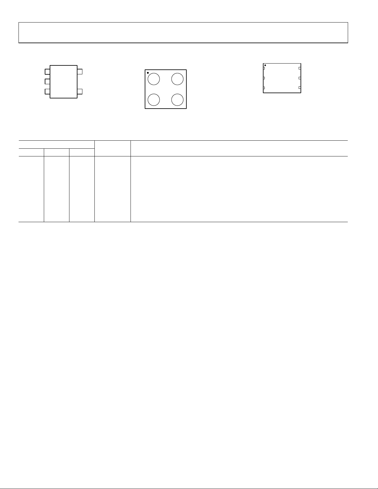
PIN CONFIGURATIONS AND FUNCTION DESCRIPTIONS
Figure 4. 5-Lead TSOT Pin Configuration Figure 5. 4-Ball WLCSP Pin Configuration Figure 6. 6-Lead LFCSP Pin Configuration
Table 5. Pin Function Descriptions
Pin No.
TSOT WLCSP LFCSP
Mnemonic Description
1 A1 6 VIN Regulator Input Supply. Bypass VIN to GND with a 1 µF or greater capacitor.
2 B2 3 GND Ground.
For automatic startup, connect EN to VIN.
4 N/A 2 NC No Connect. Not connected internally.
5 A2 1 VOUT Regulated Output Voltage. Bypass VOUT to GND with a 1 µF or greater capacitor.
N/A N/A 5 NC No Connect. Not connected internally.
N/A N/A EPAD Exposed Pad. The exposed pad must be connected to ground. The exposed pad enhances
the thermal performance of the package.
Rev. E | Page 6 of 24
Page 7
Data Sheet ADP151
3.35
3.25
3.27
3.29
3.31
3.33
–40 –5 25 85 125
V
OUT
(V)
JUNCTION T E M P E RATURE (°C)
LOAD = 10µA
LOAD = 100µA
LOAD = 1mA
LOAD = 10mA
LOAD = 100mA
LOAD = 200mA
08627-005
3.35
3.25
3.27
3.29
3.31
3.33
0.01 10001001010.1
V
OUT
(V)
I
LOAD
(mA)
08627-006
3.35
3.25
3.27
3.29
3.31
3.33
3.6 3.8 4.0 4.2 4.4 4.6 4.8 5.0 5.2 5.4
V
OUT
(V)
VIN (V)
LOAD = 10µA
LOAD = 100µA
LOAD = 1mA
LOAD = 10mA
LOAD = 100mA
LOAD = 200mA
08627-007
1k
100
10
1
–40 –5 25 85 125
GROUND CURRENT ( µ A)
JUNCTION T E M P E RATURE (°C)
LOAD = 10µA
LOAD = 100µA
LOAD = 1mA
LOAD = 10mA
LOAD = 100mA
LOAD = 200mA
08627-008
1k
10
100
0.01 10001001010.1
GROUND CURRENT ( µ A)
I
LOAD
(mA)
08627-009
GROUND CURRENT ( µ A)
VIN (V)
1k
10
100
3.6 3.8 4.0 4.2 4.4 4.6 4.8 5.0 5.2 5.4
LOAD = 10µA
LOAD = 100µA
LOAD = 1mA
LOAD = 10mA
LOAD = 100mA
LOAD = 200mA
08627-010
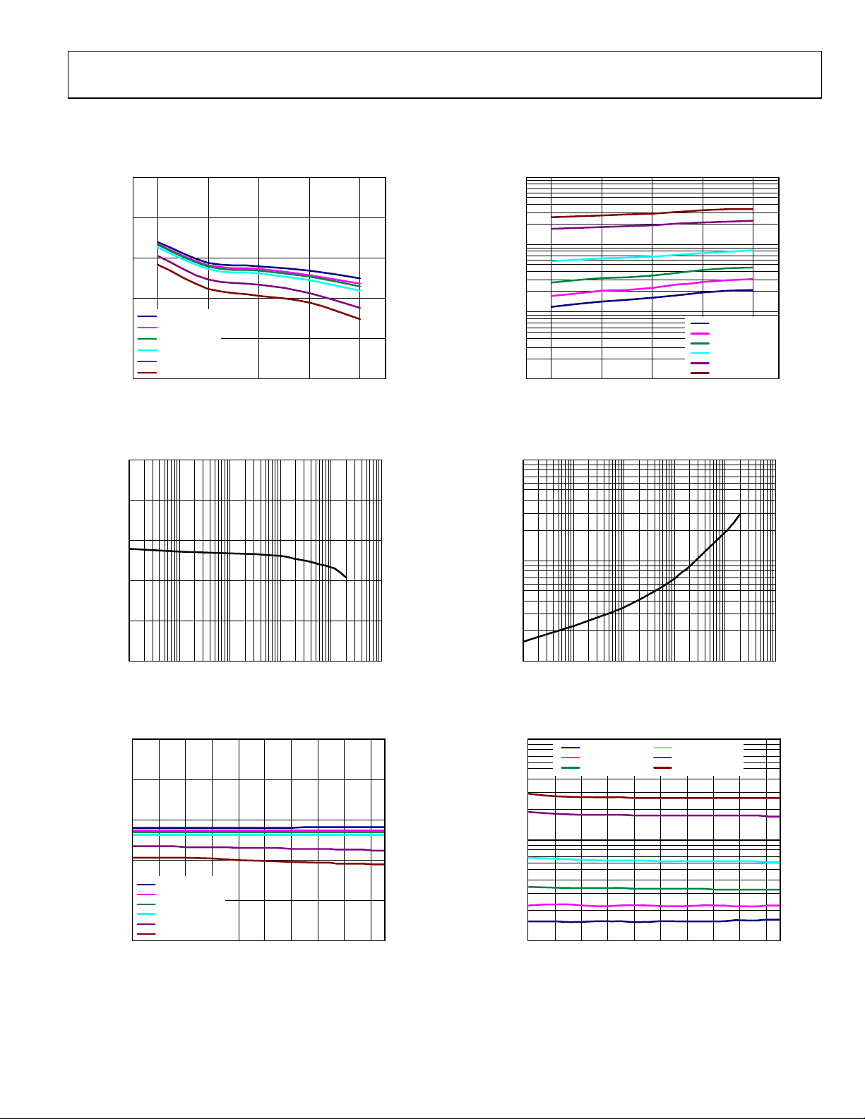
TYPICAL PERFORMANCE CHARACTERISTICS
VIN = 5 V, V
= 3.3 V, I
OUT
= 1 mA, CIN = C
OUT
= 1 µF, TA = 25°C, unless otherwise noted.
OUT
Figure 7. Output Voltage vs. Junction Temperature
Figure 8. Output Voltage vs. Load Current
Figure 10. Ground Current vs. Junction Temperature
Figure 11. Ground Current vs. Load Current
Figure 9. Output Voltage vs. Input Voltage
Figure 12. Ground Current vs. Input Voltage
Rev. E | Page 7 of 24
Page 8
ADP151 Data Sheet
0.45
0.40
0.35
0.30
0.25
0.20
0.15
0.10
0.05
0
–50 –25 1251007550250
SHUTDOWN CURRE NT (µA)
TEMPERATURE (°C)
V
IN
= 3.6V
V
IN
= 3.8V
VIN = 4.2V
V
IN
= 4.4V
VIN = 4.8V
V
IN
= 5.5V
08627-011
120
100
80
60
40
20
0
1 10 100 1000
DROPOUT VOLTAGE (mA)
I
LOAD
(mA)
08627-012
3.40
3.00
3.05
3.10
3.15
3.20
3.25
3.30
3.35
3.10 3.15 3.20 3.25
3.30 3.35 3.40 3.45 3.50 3.55
V
OUT
(V)
V
IN
(V)
I
OUT
= 1mA
I
OUT
= 5mA
I
OUT
= 10mA
I
OUT
= 50mA
I
OUT
= 100mA
I
OUT
= 200mA
08627-013
800
700
600
500
400
300
200
100
0
3.10 3.553.503.453.403.353.303.253.203.15
GROUND CURRENT ( µ A)
V
IN
(V)
I
OUT
= 1mA
I
OUT
= 5mA
I
OUT
= 10mA
I
OUT
= 50mA
I
OUT
= 100mA
I
OUT
= 200mA
08627-014
0
–10
–20
–30
–40
–50
–60
–70
–80
–90
–100
10 100 1k 10k 100k 1M 10M
PSRR (dB)
FREQUENCY ( Hz )
200mA
100mA
10mA
1mA
100µA
08627-015
0
–10
–20
–30
–40
–50
–60
–70
–80
–90
–100
10 100 1k 10k 100k 1M 10M
PSRR (dB)
FREQUENCY ( Hz )
200mA
100mA
10mA
1mA
100µA
08627-016
Figure 13. Shutdown Current vs. Temperature at Various Input Voltages
Figure 14. Dropout Voltage vs. Load Current
Figure 16. Ground Current vs. Input Voltage (in Dropout)
Figure 17. Power Supply Rejection Ratio vs. Frequency, V
= 1.2 V, VIN = 2.2 V
OUT
Figure 15. Output Voltage vs. Input Voltage (in Dropout)
Figure 18. Power Supply Rejection Ratio vs. Frequency, V
= 2.8 V, VIN = 3.3 V
OUT
Rev. E | Page 8 of 24
Page 9

Data Sheet ADP151
0
–10
–20
–30
–40
–50
–60
–70
–80
–90
–100
10 100 1k 10k 100k 1M 10M
PSRR (dB)
FREQUENCY ( Hz )
200mA
100mA
10mA
1mA
100µA
08627-017
0
–10
–20
–30
–40
–50
–60
–70
–80
–90
–100
10 100 1k 10k 100k 1M 10M
PSRR (dB)
FREQUENCY ( Hz )
V
OUT
= 3.3V, I
OUT
= 200mA
V
OUT
= 3.3V, I
OUT
= 10mA
V
OUT
= 2.8V, I
OUT
= 200mA
V
OUT
= 2.8V, I
OUT
= 10mA
V
OUT
= 1.1V, I
OUT
= 200mA
V
OUT
= 1.1V, I
OUT
= 10mA
08627-018
0
–10
–20
–30
–40
–50
–60
–70
–80
–90
–100
10 100 1k 10k 100k 1M 10M
PSRR (dB)
FREQUENCY ( Hz )
I
OUT
= 200mA, V
IN
= 3.3V
I
OUT
= 10mA, VIN =3.3V
I
OUT
= 200mA, VIN = 3.8V
I
OUT
= 10mA, VIN = 3.8V
08627-019
and Load Currents, V
= 2.8 V
14
0
1
2
3
4
5
6
7
8
9
10
11
12
13
0.001 0.01 0.1 1 10 100 1k
NOISE (µ V rms)
LOAD CURRENT ( mA)
3.3V
2.8V
1.2V
1.1V
08627-020
1000
10
100
10 100k10k1k100
NOISE SPECTRAL DENSITY (nV/ Hz)
FREQUENCY ( Hz )
3.3V
2.8V
1.2V
1.1V
08627-021
CH1 200mA CH2 50mV M20µs A CH1 64.0mA
T 10.00%
1
2
T
LOAD CURRENT
V
OUT
08627-022
Figure 19. Power Supply Rejection Ratio vs. Frequency, V
= 3.3 V, VIN = 3.8 V
OUT
Figure 20. Power Supp ly Rejection Ratio vs. Frequency at Various Output Voltages
and Load Currents, V
− VIN = 0.5 V, except for V
OUT
= 1.1 V, VIN = 2.2 V
OUT
Figure 22. Output Noise vs. Load Current and Output Voltage,
V
= 5 V, C
IN
OUT
= 1 μF
Figure 23. Output Noise Spectral Density vs. Frequency,
V
= 5 V, I
IN
= 10 mA, C
LOAD
OUT
= 1 μF
Figure 21. Power Supply Rejection Ratio vs. Frequency at Various Voltages
OUT
Figure 24. Load Transient Response, C
= 1 μF, I
IN
OUT
= 1 mA to 200 mA
LOAD
, C
Rev. E | Page 9 of 24
Page 10

ADP151 Data Sheet
CH1 1V CH2 2mV M10µs A CH1 4.56V
T 10.80%
1
2
T
INPUT VOLTAGE
V
OUT
08627-023
CH1 1V CH2 2mV M10µs A CH1 4.56V
T 10.80%
1
2
T
INPUT VOLTAGE
V
OUT
08627-024
Figure 25. Line Transient Response, CIN, C
OUT
= 1 μF, I
= 200 mA
LOAD
Figure 26. Line Transient Response, CIN, C
= 1 μF, I
OUT
LOAD
= 1 mA
Rev. E | Page 10 of 24
Page 11

Data Sheet ADP151
08627-025
REFERENCE
SHORT-CIRCUIT,
UVLO, AND
THERMAL
PROTECT
SHUTDOWN
R1
R2
R
EN
VOUTVIN
GND
EN
THEORY OF OPERATION
The ADP151 is an ultralow noise, low quiescent current, low
dropout linear regulator that operates from 2.2 V to 5.5 V and
can provide up to 200 mA of output current. Drawing a low
265 μA of quiescent current (typical) at full load makes the
ADP151 ideal for battery-operated portable equipment.
Shutdown current consumption is typically 200 nA.
Using new innovative design techniques, the ADP151 provides
superior noise performance for noise-sensitive analog and RF
applications without the need for a noise bypass capacitor. The
ADP151 is also optimized for use with small 1 µF ceramic
capacitors.
Internally, the ADP151 consists of a reference, an error amplifier, a
feedback voltage divider, and a PMOS pass transistor. Output
current is delivered via the PMOS pass device, which is controlled
by the error amplifier. The error amplifier compares the reference
voltage with the feedback voltage from the output and amplifies
the difference. If the feedback voltage is lower than the reference
voltage, the gate of the PMOS device is pulled lower, allowing
more current to pass and increasing the output voltage. If the
feedback voltage is higher than the reference voltage, the gate of
the PMOS device is pulled higher, allowing less current to pass
and decreasing the output voltage.
An internal pull-down resistor on the EN input holds the input
low when the pin is left open.
The ADP151 is available in 16 output voltage options, ranging
from 1.1 V to 3.3 V. The ADP151 uses the EN pin to enable and
disable the VOUT pin under normal operating conditions. When
EN is high, VOUT turns on; when EN is low, VOUT turns off.
For automatic startup, EN can be tied to VIN.
Figure 27. Internal Block Diagram
Rev. E | Page 11 of 24
Page 12

ADP151 Data Sheet
CH1 200mA CH2 50mV M20µs A CH1 64mA
T 10.00%
1
2
T
LOAD CURRENT
V
OUT
08627-026
1.2
1.0
0.8
0.6
0.4
0.2
0
0 2 4 6 8 10
CAPACITANCE (µ F)
VOLTAGE BIAS
08627-027
APPLICATIONS INFORMATION
CAPACITOR SELECTION
Output Capacitor
The ADP151 is designed for operation with small, space-saving
ceramic capacitors but can function with most commonly used
capacitors as long as care is taken with regard to the effective
series resistance (ESR) value. The ESR of the output capacitor
affects the stability of the LDO control loop. A minimum of 1 µF
capacitance with an ESR of 1 Ω or less is recommended to ensure
the stability of the ADP151. Transient response to changes in load
current is also affected by output capacitance. Using a larger value
of output capacitance improves the transient response of the
ADP151 to large changes in load current. Figure 28 shows the
transient responses for an output capacitance value of 1 µF.
Figure 29 depicts the capacitance vs. voltage bias characteristic
of an 0402, 1 µF, 10 V X5R capacitor. The voltage stability of a
capacitor is strongly influenced by the capacitor size and voltage
rating. In general, a capacitor in a larger package or higher voltage
rating exhibits better stability. The temperature variation of the
X5R dielectric is ~±15% over the −40°C to +85°C temperature
range and is not a function of package or voltage rating.
Figure 29. Capacitance vs. Voltage Bias Characteristic
Use Equation 1 to determine the worst-case capacitance, accounting
for capacitor variation over temperature, component tolerance,
and voltage.
C
= C
EFF
Figure 28. Output Transient Response, C
OUT
= 1 µF
Input Bypass Capacitor
Connecting a 1 µF capacitor from VIN to GND reduces
the circuit sensitivity to the printed circuit board (PCB) layout,
especially when long input traces or high source impedance
are encountered. If greater than 1 µF of output capacitance is
required, the input capacitor should be increased to match it.
Input and Output Capacitor Properties
Any good quality ceramic capacitor can be used with the
ADP151, as long as it meets the minimum capacitance and
maximum ESR requirements. Ceramic capacitors are manufactured with a variety of dielectrics, each with different behavior
over temperature and applied voltage. Capacitors must have an
adequate dielectric to ensure the minimum capacitance over the
necessary temperature range and dc bias conditions. X5R or X7R
dielectrics with a voltage rating of 6.3 V or 10 V are recommended.
Y5V and Z5U dielectrics are not recommended, due to their
poor temperature and dc bias characteristics.
where:
C
is the effective capacitance at the operating voltage.
BIAS
TEMPCO is the worst-case capacitor temperature coefficient.
TOL is the worst-case component tolerance.
In this example, the worst-case temperature coefficient (TEMPCO)
over −40°C to +85°C is assumed to be 15% for an X5R dielectric.
The tolerance of the capacitor (TOL) is assumed to be 10%, and
C
is 0.94 μF at 1.8 V, as shown in Figure 29.
BIAS
Substituting these values in Equation 1 yields
C
EFF
Therefore, the capacitor chosen in this example meets the
minimum capacitance requirement of the LDO over temperature and tolerance at the chosen output voltage.
To guarantee the performance of the ADP151, it is imperative
that the effects of dc bias, temperature, and tolerances on the
behavior of the capacitors be evaluated for each application.
× (1 − TEMPCO) × (1 − TOL) (1)
BIAS
= 0.94 μF × (1 − 0.15) × (1 − 0.1) = 0.719 μF
Rev. E | Page 12 of 24
Page 13

Data Sheet ADP151
3.0
2.5
2.0
1.5
0.5
1.0
0
0 0.5 1.0 1.5 2.0 2.5
V
OUT
ENABLE VOLTAGE
08627-028
1200
1000
800
600
200
400
0
2.0 2.5 3.0 3.5 4.5 5.04.0 5.5
ENABLE VOLTAGE
INPUT VOLTAGE
VEN RISE
V
EN
FALL
08627-029
3.5
3.0
2.5
2.0
1.5
1.0
0.5
0
0 45040035030025020015010050
ENABLE VOLTAGE
TIME (µs)
ENABLE
3.3V
2.8V
1.1V
08627-030
08627-131
U1
1
2
3
5
4
C2
C1
V
OUT
V
IN
VOUT
NC
VIN
GND
EN
C3
R2
V
OFFSET
R1
V
OUT
= V
LDO
× (1 + R2/R1)
ENABLE FEATURE
The ADP151 uses the EN pin to enable and disable the VOUT
pin under normal operating conditions. As shown in Figure 30,
when a rising voltage on EN crosses the active threshold, VOUT
turns on. When a falling voltage on EN crosses the inactive
threshold, VOUT turns off.
Figure 30. ADP151 Typical EN Pin Operation
As shown in Figure 30, the EN pin has hysteresis built in. This
prevents on/off oscillations that can occur due to noise on the
EN pin as it passes through the threshold points.
The EN pin active/inactive thresholds are derived from the VIN
voltage. Therefore, these thresholds vary with changing input
voltage. Figure 31 shows typical EN active/inactive thresholds
when the input voltage varies from 2.2 V to 5.5 V.
Figure 31. Typical EN Pin Thresholds vs. Input Voltage
The ADP151 uses an internal soft start to limit the inrush current
when the output is enabled. The start-up time for the 3.3 V
option is approximately 160 μs from the time the EN active
threshold is crossed to when the output reaches 90% of its final
value. As shown in Figure 32, the start-up time is dependent on
the output voltage setting.
Figure 32. Typical Start-Up Behavior
ADJUSTABLE OUTPUT VOLTAGE OPERATION
The unique architecture of the ADP151 makes an adjustable
version difficult to implement in silicon. However, it is possible
to create an adjustable regulator at the expense of increasing the
Rev. E | Page 13 of 24
quiescent current of the regulator circuit.
The ADP151, and similar LDOs, are designed to regulate the
output voltage, V
, appearing at the VOUT pin with respect
OUT
to the GND pin. If the GND pin is at a potential other than 0 V
(for example, at V
V
. By taking advantage of this behavior, it is possible to
OFFSET
), the ADP151 output voltage is V
OFFSET
OUT
+
create an adjustable ADP151 circuit that retains most of the
desirable characteristics of the ADP151.
Figure 33. Adjustable LDO Using the ADP151
The circuit shown in Figure 33 is an example of an adjustable
LDO using the ADP151. A stable V
voltage is created by
OFFSET
passing a known current through R2. The current through R2 is
determined by the voltage across R1. Because the voltage across
R1 is set by the voltage between VOUT and GND, the current
passing through R2 is fixed, and V
OFFSET
is stable.
To minimize the effect variation of the ADP151 ground current
(I
) with load, it is best to keep R1 as small as possible. It is
GND
also best to size the current passing through R2 to at least 20×
greater than the maximum expected ground current.
To create a 4 V LDO circuit, start with the 3.3 V version of the
ADP151 to minimize the value of R2. Because V
V
must be 0.7 V, and the current through R2 must be 7 mA.
OFFSET
OUT
is 4 V,
R1 is, therefore, 3.3 V/7 mA or 471 Ω. A 470 Ω standard value
introduces less than 1% error. Capacitor C3 is necessary to stabilize
the LDO; a value of 1 μF is adequate.
Page 14

ADP151 Data Sheet
4.04
4.03
4.02
4.01
4.00
3.99
3.98
3.97
3.96
–40 –5 25 85 125
V
OUT
(V)
JUNCTION T E M P E RATURE (°C)
08627-132
LOAD = 10mA
LOAD = 20mA
LOAD = 50mA
LOAD = 100mA
LOAD = 150mA
LOAD = 200mA
V
OUT
(V)
VIN (V)
08627-133
LOAD = 10mA
LOAD = 20mA
LOAD = 50mA
LOAD = 100mA
LOAD = 150mA
LOAD = 200mA
4.040
4.035
4.030
4.025
4.020
4.015
4.010
4.005
4.000
4.4 5.2 5.44.84.6 5.0
11
10
9
8
1 100 1k10
NOISE (µ V rms)
LOAD CURRENT ( mA)
08627-134
0
–10
–20
–30
–40
–50
–60
–70
–80
–90
–100
10 100 1k 10k 100k 1M 10M
FREQUENCY ( Hz )
PSRR (dB)
08627-049
200mA
100mA
50mA
10mA
0
–10
–20
–30
–40
–50
–60
–70
–80
–90
–100
10 100 1k 10k 100k 1M 10M
FREQUENCY ( Hz )
PSRR (dB)
08627-050
200mA
100mA
50mA
10mA
Figure 34 through Figure 38 show the typical performance of the
4 V LDO circuit.
The noise performance of the 4 V LDO circuit is only about 1 μV
worse than the same LDO used at 3.3 V because the output noise of
the circuit is almost solely determined by the LDO and not the
external components. The small difference may be attributed to the
internally generated noise in the LDO ground current working with
R2. By keeping R2 small, this noise contribution can be minimized.
The PSRR of the 4 V circuit is as much as 10 dB poorer than the
3.3 V LDO with 500 mV of headroom because the ground current
of the LDO varies slightly with input voltage. This, in turn,
modulates V
increasing the headroom to 1 V, the PSRR performance is
nearly restored to the performance of the fixed output LDO.
and reduces the PSRR of the regulator. By
OFFSET
Figure 36. 4 V LDO Circuit, Typical RMS Output Noise, 10 Hz to 100 kHz
Figure 34. 4 V LDO Circuit, Typical Load Regulation over Temperature
Figure 35. 4 V LDO Circuit, Typical Line Regulation over Load Current
Figure 37. 4 V LDO Circuit, Typical PSRR vs. Load Current, 1 V Headroom
Figure 38. 4 V LDO Circuit, Typical PSRR vs. Load Current, 500 mV Headroom
Rev. E | Page 14 of 24
Page 15

Data Sheet ADP151
CURRENT-LIMIT AND THERMAL OVERLOAD PROTECTION
The ADP151 is protected against damage due to excessive
power dissipation by current and thermal overload protection
circuits. The ADP151 is designed to current limit when the
output load reaches 300 mA (typical). When the output load
exceeds 300 mA, the output voltage is reduced to maintain a
constant current limit.
Thermal overload protection is included, which limits the
junction temperature to a maximum of 150°C (typical). Under
extreme conditions (that is, high ambient temperature and
power dissipation) when the junction temperature starts to
rise above 150°C, the output is turned off, reducing the output
current to 0. When the junction temperature drops below
135°C, the output is turned on again, and output current is
restored to its nominal value.
Consider the case where a hard short from VOUT to ground
occurs. At first, the ADP151 current limits, so that only 300 mA
is conducted into the short. If self-heating of the junction
causes its temperature to rise above 150°C, thermal shutdown
activates, turning off the output and reducing the output current
to 0. As the junction temperature cools and drops below
135°C, the output turns on and conducts 300 mA into the
short, again causing the junction temperature to rise above
150°C. This thermal oscillation between 135°C and 150°C causes a
current oscillation between 300 mA and 0 mA that continues
as long as the short remains at the output.
Current- and thermal-limit protections are intended to protect
the device against accidental overload conditions. For reliable
operation, device power dissipation must be externally limited
so that junction temperatures do not exceed 125°C.
THERMAL CONSIDERATIONS
In most applications, the ADP151 does not dissipate much heat
due to its high efficiency. However, in applications with a high
ambient temperature and a high supply voltage to output voltage
differential, the heat dissipated in the package can cause the
junction temperature of the die to exceed the maximum junction
temperature of 125°C.
When the junction temperature exceeds 150°C, the converter
enters thermal shutdown. It recovers only after the junction
temperature has decreased below 135°C to prevent any permanent
damage. Therefore, thermal analysis for the chosen application
is very important to guarantee reliable performance over all
conditions. The junction temperature of the die is the sum of
the ambient temperature of the environment and the temperature rise of the package due to the power dissipation, as shown
in Equation 2.
To guarantee reliable operation, the junction temperature of
the ADP151 must not exceed 125°C. To ensure that the junction
temperature stays below this maximum value, the user must be
aware of the parameters that contribute to junction temperature
changes. These parameters include ambient temperature, power
dissipation in the power device, and thermal resistances between
the junction and ambient air (θ
). The θJA number is dependent
JA
on the package assembly compounds that are used and the amount
of copper used to solder the package GND pins to the PCB.
Table 6 shows typical θ
values of the 5-lead TSOT, 6-lead
JA
L FC SP, an d 4 -ball WLCSP packages for various PCB copper sizes.
Table 7 shows the typical Ψ
values of the 5-lead TSOT, 6-lead
JB
LFCSP, and 4-ball WLCSP.
Table 6. Typical θ
Copper Size (mm2)
Values
JA
θ
(°C/W)
JA
TSOT WLCSP LFCSP
01 170 260 231.2
50 152 159 161.8
100 146 157 150.1
300 134 153 111.5
500 131 151 91.8
1
Device soldered to minimum size pin traces.
Table 7. Typical ΨJB Values
Model ΨJB (°C/W)
TSOT 43
WLCSP 58
LFCSP 28.3
The junction temperature of the ADP151 can be calculated
from the following equation:
T
= TA + (PD × θJA) (2)
J
where:
T
is the ambient temperature.
A
P
is the power dissipation in the die, given by
D
P
= [(VIN − V
D
OUT
) × I
] + (VIN × I
LOAD
) (3)
GND
where:
I
is the load current.
LOAD
I
is the ground current.
GND
V
and V
IN
are input and output voltages, respectively.
OUT
Power dissipation due to ground current is quite small and can
be ignored. Therefore, the junction temperature equation
simplifies to the following:
T
= TA + {[(VIN − V
J
OUT
) × I
] × θJA} (4)
LOAD
As shown in Equation 4, for a given ambient temperature, input-tooutput voltage differential, and continuous load current, there
exists a minimum copper size requirement for the PCB to ensure
that the junction temperature does not rise above 125°C. Figure 39
through Figure 59 show junction temperature calculations for
various ambient temperatures, load currents, V
-to-V
IN
OUT
differentials, and areas of PCB copper.
Rev. E | Page 15 of 24
Page 16

ADP151 Data Sheet
140
120
100
80
60
40
20
0
0.3 4.84.33.83.32.82.31.81.30.8
V
IN
– V
OUT
(V)
JUNCTION T E M P E RATURE, T
J
(°C)
MAXIMUM JUNCT ION TEMPE RATURE
I
LOAD
= 1mA
I
LOAD
= 10mA
I
LOAD
= 50mA
I
LOAD
= 100mA
I
LOAD
= 150mA
I
LOAD
= 200mA
08627-031
140
120
100
80
60
40
20
0
0.3 4.84.33.83.32.82.31.81.30.8
V
IN
– V
OUT
(V)
JUNCTION T E M P E RATURE, T
J
(°C)
MAXIMUM JUNCT ION TEMPE RATURE
I
LOAD
= 1mA
I
LOAD
= 10mA
I
LOAD
= 50mA
I
LOAD
= 100mA
I
LOAD
= 150mA
I
LOAD
= 200mA
08627-032
140
120
100
80
60
40
20
0
0.3 4.84.33.83.32.82.31.81.30.8
V
IN
– V
OUT
(V)
JUNCTION T E M P E RATURE, T
J
(°C)
MAXIMUM JUNCT ION TEMPE RATURE
I
LOAD
= 1mA
I
LOAD
= 10mA
I
LOAD
= 50mA
I
LOAD
= 100mA
I
LOAD
= 150mA
I
LOAD
= 200mA
08627-033
140
120
100
80
60
40
20
0
0.3 4.84.33.83.32.82.31.81.30.8
V
IN
– V
OUT
(V)
JUNCTION T E M P E RATURE, T
J
(°C)
I
LOAD
= 1mA
I
LOAD
= 10mA
I
LOAD
= 50mA
I
LOAD
= 100mA
I
LOAD
= 150mA
I
LOAD
= 200mA
MAXIMUM JUNCT ION TEMPE RATURE
08627-034
140
120
100
80
60
40
20
0
0.3 4.84.33.83.32.82.31.81.30.8
V
IN
– V
OUT
(V)
JUNCTION T E M P E RATURE, T
J
(°C)
I
LOAD
= 1mA
I
LOAD
= 10mA
I
LOAD
= 50mA
I
LOAD
= 100mA
I
LOAD
= 150mA
I
LOAD
= 200mA
MAXIMUM JUNCT ION TEMPE RATURE
08627-035
140
120
100
80
60
40
20
0
0.3 4.84.33.83.32.82.31.81.30.8
V
IN
– V
OUT
(V)
JUNCTION T E M P E RATURE, T
J
(°C)
I
LOAD
= 1mA
I
LOAD
= 10mA
I
LOAD
= 50mA
I
LOAD
= 100mA
I
LOAD
= 150mA
I
LOAD
= 200mA
MAXIMUM JUNCT ION TEMPE RATURE
08627-036
Figure 39. WLCSP 500 mm2 of PCB Copper, TA = 25°C
Figure 40. WLCSP 100 mm2 of PCB Copper, TA = 25°C
Figure 42. WLCSP 500 mm2 of PCB Copper, TA = 50°C
Figure 43. WLCSP 100 mm2 of PCB Copper, TA = 50°C
Figure 41. WLCSP 50 mm2 of PCB Copper, TA = 25°C
Figure 44. WLCSP 50 mm2 of PCB Copper, TA = 50°C
Rev. E | Page 16 of 24
Page 17

Data Sheet ADP151
140
120
100
80
60
40
20
0
0.3 4.84.33.83.32.82.31.81.30.8
V
IN
– V
OUT
(V)
JUNCTION T E M P E RATURE, T
J
(°C)
I
LOAD
= 1mA
I
LOAD
= 10mA
I
LOAD
= 50mA
I
LOAD
= 100mA
I
LOAD
= 150mA
I
LOAD
= 200mA
MAXIMUM JUNCT ION TEMPE RATURE
08627-037
140
120
100
80
60
40
20
0
0.3 4.84.33.83.32.82.31.81.30.8
V
IN
– V
OUT
(V)
JUNCTION T E M P E RATURE, T
J
(°C)
I
LOAD
= 1mA
I
LOAD
= 10mA
I
LOAD
= 50mA
I
LOAD
= 100mA
I
LOAD
= 150mA
I
LOAD
= 200mA
MAXIMUM JUNCT ION TEMPE RATURE
08627-038
140
120
100
80
60
40
20
0
0.3 4.84.33.83.32.82.31.81.30.8
V
IN
– V
OUT
(V)
JUNCTION T E M P E RATURE, T
J
(°C)
I
LOAD
= 1mA
I
LOAD
= 10mA
I
LOAD
= 50mA
I
LOAD
= 100mA
I
LOAD
= 150mA
I
LOAD
= 200mA
MAXIMUM JUNCT ION TEMPE RATURE
08627-039
140
120
100
80
60
40
20
0
0.3 4.84.33.83.32.82.31.81.30.8
V
IN
– V
OUT
(V)
JUNCTION T E M P E RATURE, T
J
(°C)
I
LOAD
= 1mA
I
LOAD
= 10mA
I
LOAD
= 50mA
I
LOAD
= 100mA
I
LOAD
= 150mA
I
LOAD
= 200mA
MAXIMUM JUNCT ION TEMPE RATURE
08627-040
140
120
100
80
60
40
20
0
0.3 4.84.33.83.32.82.31.81.30.8
V
IN
– V
OUT
(V)
JUNCTION T E M P E RATURE, T
J
(°C)
I
LOAD
= 1mA
I
LOAD
= 10mA
I
LOAD
= 50mA
I
LOAD
= 100mA
I
LOAD
= 150mA
I
LOAD
= 200mA
MAXIMUM JUNCT ION TEMPE RATURE
08627-041
140
120
100
80
60
40
20
0
0.3 4.84.33.83.32.82.31.81.30.8
V
IN
– V
OUT
(V)
JUNCTION T E M P E RATURE, T
J
(°C)
I
LOAD
= 1mA
I
LOAD
= 10mA
I
LOAD
= 50mA
I
LOAD
= 100mA
I
LOAD
= 150mA
I
LOAD
= 200mA
MAXIMUM JUNCT ION TEMPE RATURE
08627-042
Figure 45. TSOT 500 mm2 of PCB Copper, TA = 25°C
Figure 46. TSOT 100 mm2 of PCB Copper, TA = 25°C
Figure 48. TSOT 500 mm2 of PCB Copper, TA = 50°C
Figure 49. TSOT 100 mm2 of PCB Copper, TA = 50°C
Figure 47. TSOT 50 mm2 of PCB Copper, TA = 25°C
Figure 50. TSOT 50 mm2 of PCB Copper, TA = 50°C
Rev. E | Page 17 of 24
Page 18

ADP151 Data Sheet
140
120
100
80
60
40
20
0
0.3 4.84.33.83.32.82.31.81.30.8
V
IN
– V
OUT
(V)
JUNCTION T E M P E RATURE, T
J
(°C)
I
LOAD
= 1mA
I
LOAD
= 10mA
I
LOAD
= 50mA
I
LOAD
= 100mA
I
LOAD
= 150mA
I
LOAD
= 200mA
MAXIMUM JUNCT ION TEMPE RATURE
08627-051
140
120
100
80
60
40
20
0
0.3 4.84.33.83.32.82.31.81.30.8
V
IN
– V
OUT
(V)
JUNCTION T E M P E RATURE, T
J
(°C)
I
LOAD
= 1mA
I
LOAD
= 10mA
I
LOAD
= 50mA
I
LOAD
= 100mA
I
LOAD
= 150mA
I
LOAD
= 200mA
MAXIMUM JUNCT ION TEMPE RATURE
08627-052
140
120
100
80
60
40
20
0
0.3 4.84.33.83.32.82.31.81.30.8
V
IN
– V
OUT
(V)
JUNCTION T E M P E RATURE, T
J
(°C)
I
LOAD
= 1mA
I
LOAD
= 10mA
I
LOAD
= 50mA
I
LOAD
= 100mA
I
LOAD
= 150mA
I
LOAD
= 200mA
MAXIMUM JUNCT ION TEMPE RATURE
08627-053
140
120
100
80
60
40
20
0
0.3 4.84.33.83.32.82.31.81.30.8
V
IN
– V
OUT
(V)
JUNCTION T E M P E RATURE, T
J
(°C)
I
LOAD
= 1mA
I
LOAD
= 10mA
I
LOAD
= 50mA
I
LOAD
= 100mA
I
LOAD
= 150mA
I
LOAD
= 200mA
MAXIMUM JUNCT ION TEMPE RATURE
08627-055
140
120
100
80
60
40
20
0
0.3 4.84.33.83.32.82.31.81.30.8
V
IN
– V
OUT
(V)
JUNCTION T E M P E RATURE, T
J
(°C)
I
LOAD
= 1mA
I
LOAD
= 10mA
I
LOAD
= 50mA
I
LOAD
= 100mA
I
LOAD
= 150mA
I
LOAD
= 200mA
MAXIMUM JUNCT ION TEMPE RATURE
08627-056
140
120
100
80
60
40
20
0
0.3 4.84.33.83.32.82.31.81.30.8
V
IN
– V
OUT
(V)
JUNCTION T E M P E RATURE, T
J
(°C)
I
LOAD
= 1mA
I
LOAD
= 10mA
I
LOAD
= 50mA
I
LOAD
= 100mA
I
LOAD
= 150mA
I
LOAD
= 200mA
MAXIMUM
JUNCTION
TEMPERATURE
08627-057
Figure 51. LFCSP 500 mm2 of PCB Copper, TA = 25°C
Figure 52. LFCSP 100 mm2 of PCB Copper, TA = 25°C
Figure 54. LFCSP 500 mm2 of PCB Copper, TA = 50°C
Figure 55. LFCSP 100 mm2 of PCB Copper, TA = 50°C
Figure 53. LFCSP 50 mm2 of PCB Copper, TA = 25°C
Figure 56. LFCSP 50 mm2 of PCB Copper, TA = 50°C
Rev. E | Page 18 of 24
Page 19

Data Sheet ADP151
140
120
100
80
60
40
20
0
0.3 4.84.33.83.32.82.31.81.30.8
V
IN
– V
OUT
(V)
JUNCTION T E M P E RATURE, T
J
(°C)
I
LOAD
= 1mA
I
LOAD
= 10mA
I
LOAD
= 50mA
I
LOAD
= 100mA
I
LOAD
= 150mA
I
LOAD
= 200mA
MAXIMUM JUNCT ION TEMPE RATURE
08627-043
140
120
100
80
60
40
20
0
0.3 4.84.33.83.32.82.31.81.30.8
V
IN
– V
OUT
(V)
JUNCTION T E M P E RATURE, T
J
(°C)
I
LOAD
= 1mA
I
LOAD
= 10mA
I
LOAD
= 50mA
I
LOAD
= 100mA
I
LOAD
= 150mA
I
LOAD
= 200mA
MAXIMUM JUNCT ION TEMPE RATURE
08627-044
140
120
100
80
60
40
20
0
0.3 5.34.33.32.3
1.3
V
IN
– V
OUT
(V)
JUNCTION T E M P E RATURE, T
J
(°C)
I
LOAD
= 1mA
I
LOAD
= 10mA
I
LOAD
= 50mA
I
LOAD
= 100mA
I
LOAD
= 150mA
I
LOAD
= 200mA
MAXIMUM JUNCT ION TEMPE RATURE
08627-059
In the case where the board temperature is known, use the
thermal characterization parameter, Ψ
junction temperature rise (see Figure 57 and Figure 58).
Maximum junction temperature (T
board temperature (T
) and power dissipation (PD) using the
B
following formula:
T
= TB + (PD × ΨJB) (5)
J
The typical value of Ψ
is 58°C/W for the 4-ball WLCSP package,
JB
43°C/W for the 5-lead TSOT package, and 28.3°C/W for the 6-lead
LFCSP package.
, to estimate the
JB
) is calculated from the
J
Figure 58. TSOT, T
= 85°C
A
Figure 57. WLCSP, T
= 85°C
A
Figure 59. LFCSP, T
= 85°C
A
Rev. E | Page 19 of 24
Page 20

ADP151 Data Sheet
08627-045
08627-046
08627-054
PRINTED CIRCUIT BOARD LAYOUT CONSIDERATIONS
Heat dissipation from the package can be improved by increasing
the amount of copper attached to the pins of the ADP151.
However, as listed in Table 6, a point of diminishing returns
is eventually reached, beyond which an increase in the copper
size does not yield significant heat dissipation benefits.
Place the input capacitor as close as possible to the VIN and
GND pins. Place the output capacitor as close as possible to the
VOUT and GND pins. Use of 0402 or 0603 size capacitors and
resistors achieves the smallest possible footprint solution on
boards where area is limited.
Figure 61. Example WLCSP PCB Layout
Figure 60. Example TSOT PCB Layout
Figure 62. Example LFCSP PCB Layout
Rev. E | Page 20 of 24
Page 21

Data Sheet ADP151
100708-A
*
COMPLI ANT TO JEDEC STANDARDS MO-193-AB WITH
THE EXCEPTION OF P ACKAGE HEIGHT AND THICKNESS.
1.60 BSC
2.80 BSC
1.90
BSC
0.95 BSC
0.20
0.08
0.60
0.45
0.30
8°
4°
0°
0.50
0.30
0.10 MAX
*
1.00 MAX
*
0.90 MAX
0.70 MIN
2.90 BSC
5 4
1 2 3
SEATING
PLANE
011509-A
0.050 NOM
COPLANARITY
0.800
0.760 SQ
0.720
0.230
0.200
0.170
0.280
0.260
0.240
0.660
0.600
0.540
0.430
0.400
0.370
BOTTOM VIEW
(BALL SIDE UP)
TOP VIEW
(BALL SI DE DOWN)
A
12
B
SEATING
PLANE
0.40
BALL PITCH
BALL A1
IDENTIFIER
1.70
1.60
1.50
0.425
0.350
0
.275
TOP VIEW
6
1
4
3
0.35
0.30
0.25
BOTTOM VIEW
PIN 1 INDEX
AREA
SEA
TING
PLANE
0.60
0.55
0.50
1.10
1.00
0.90
0.20 REF
0.05 MAX
0.02 NOM
2.00
BSC SQ
0.65 BSC
EXPOSED
PAD
PIN 1
INDICATOR
(R 0.15)
FOR PROPER CONNECTION OF
THE EXPOSED PAD, REFER TO
THE PIN CONFIGURATION AND
FUNCTION DESCRIPTIONS
SECTION OF THIS DATA SHEET.
05-04-2010-A
OUTLINE DIMENSIONS
Figure 63. 5-Lead Thin Small Outline Transistor Package [TSOT]
(UJ-5)
Dimensions show in millimeters
Figure 64. 4-Ball Wafer Level Chip Scale Package [WLCSP]
(CB-4-3)
Dimensions show in millimeters
Figure 65. 6-Lead Lead Frame Chip Scale Package [LFCSP_UD]
2.00 mm × 2.00 mm Body, Ultra Thin, Dual L ead
(CP-6-3)
Dimensions show in millimeters
Rev. E | Page 21 of 24
Page 22

ADP151 Data Sheet
Model1
Temperature Range
Output Voltage (V)2
Package Description
Package Option3
Branding
ADP151AUJZ-1.2-R7
–40°C to +125°C
1.2
5-Lead TSOT
UJ-5
LF6
ADP151CB-3.3-EVALZ
Evaluation Board
ORDERING GUIDE
ADP151ACBZ-1.1-R7 –40°C to +125°C 1.1 4-Ball WLCSP CB-4-1 8R
ADP151ACBZ-1.2-R7 –40°C to +125°C 1.2 4-Ball WLCSP CB-4-3 4R
ADP151ACBZ-1.5-R7 –40°C to +125°C 1.5 4-Ball WLCSP CB-4-3 4S
ADP151ACBZ-1.8-R7 –40°C to +125°C 1.8 4-Ball WLCSP CB-4-3 4T
ADP151ACBZ-2.5-R7 –40°C to +125°C 2.5 4-Ball WLCSP CB-4-3 4U
ADP151ACBZ-2.6-R7 –40°C to +125°C 2.6 4-Ball WLCSP CB-4-3 8Q
ADP151ACBZ-2.75-R7 –40°C to +125°C 2.75 4-Ball WLCSP CB-4-3 4V
ADP151ACBZ-2.8-R7 –40°C to +125°C 2.8 4-Ball WLCSP CB-4-3 4X
ADP151ACBZ-2.85-R7 –40°C to +125°C 2.85 4-Ball WLCSP CB-4-3 4Y
ADP151ACBZ-3.0-R7 –40°C to +125°C 3.0 4-Ball WLCSP CB-4-3 4Z
ADP151ACBZ-3.3-R7 –40°C to +125°C 3.3 4-Ball WLCSP CB-4-3 50
ADP151ACBZ-2.1-R7 –40°C to +125°C 2.1 4-Ball WLCSP CB-4-3 5E
ADP151AUJZ-1.5-R7 –40°C to +125°C 1.5 5-Lead TSOT UJ-5 LF7
ADP151AUJZ-1.8-R7 –40°C to +125°C 1.8 5-Lead TSOT UJ-5 LF8
ADP151AUJZ-2.5-R7 –40°C to +125°C 2.5 5-Lead TSOT UJ-5 LF9
ADP151AUJZ-2.8-R7 –40°C to +125°C 2.8 5-Lead TSOT UJ-5 LFG
ADP151AUJZ-3.0-R7 –40°C to +125°C 3.0 5-Lead TSOT UJ-5 LFH
ADP151AUJZ-3.3-R7 –40°C to +125°C 3.3 5-Lead TSOT UJ-5 LFJ
ADP151ACPZ-1.2-R7 –40°C to +125°C 1.2 6-Lead LFCSP_UD CP-6-3 LF6
ADP151ACPZ-1.5-R7 –40°C to +125°C 1.5 6-Lead LFCSP_UD CP-6-3 LF7
ADP151ACPZ-1.8-R7 –40°C to +125°C 1.8 6-Lead LFCSP_UD CP-6-3 LF8
ADP151ACPZ-2.5-R7 –40°C to +125°C 2.5 6-Lead LFCSP_UD CP-6-3 LF9
ADP151ACPZ-2.7-R7 –40°C to +125°C 2.7 6-Lead LFCSP_UD CP-6-3 LKZ
ADP151ACPZ-2.8-R7 –40°C to +125°C 2.8 6-Lead LFCSP_UD CP-6-3 LFG
ADP151ACPZ-3.0-R7 –40°C to +125°C 3.0 6-Lead LFCSP_UD CP-6-3 LFH
ADP151ACPZ-3.3-R7 –40°C to +125°C 3.3 6-Lead LFCSP_UD CP-6-3 LFJ
ADP151UJZ-REDYKIT Evaluation Board Kit
ADP151CPZ-REDYKIT Evaluation Board Kit
1
Z = RoHS Compliant Part.
2
For additional voltage options for the ADP151ACBZ package option, contact a local Analog Devices, Inc., sales or distribution representative.
3
The ADP151ACBZ package option is halide free.
Rev. E | Page 22 of 24
Page 23

Data Sheet ADP151
NOTES
Rev. E | Page 23 of 24
Page 24

ADP151 Data Sheet
NOTES
©2010–2012 Analog Devices, Inc. All rights reserved. Trademarks and
registered trademarks are the property of their respective owners.
D08627-0-4/12(E)
Rev. E | Page 24 of 24
 Loading...