

Page 1
Micropower
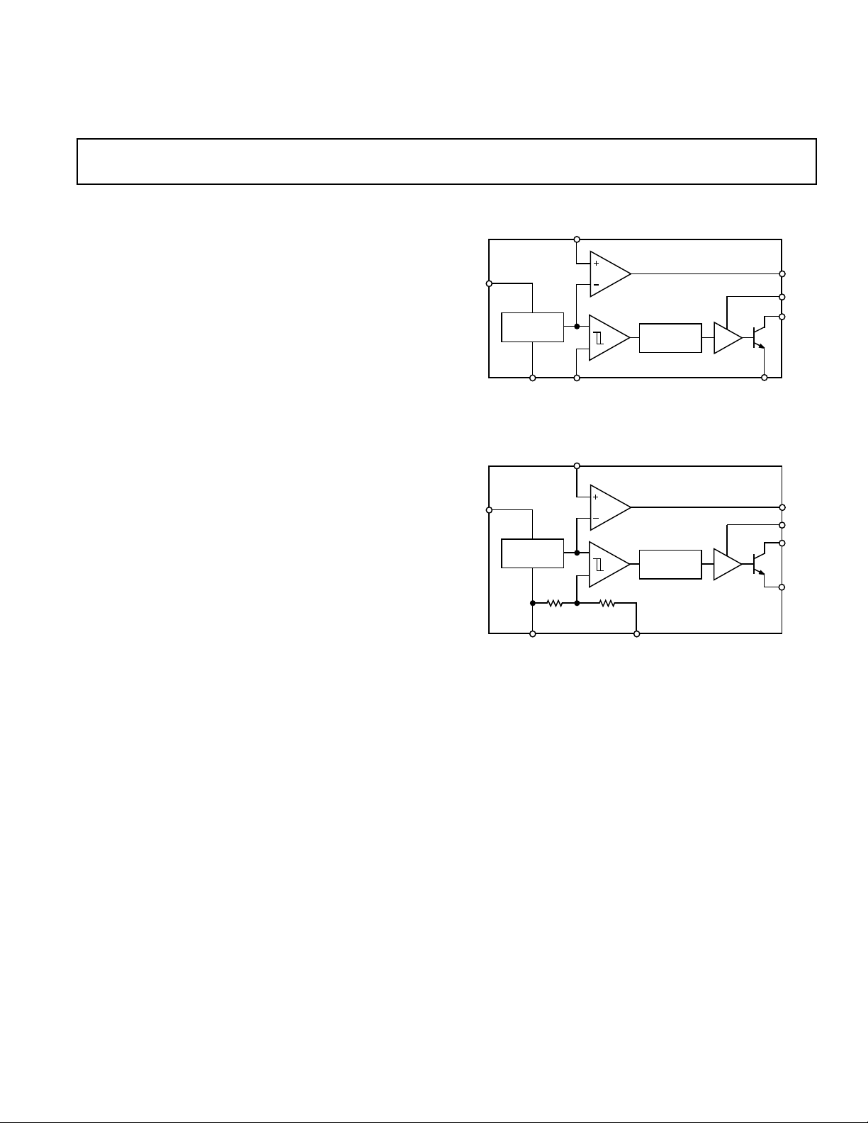
SET
V
IN
GAIN BLOCK/
ERROR AMP
COMPARATOR
SW2
FBGND
SW1
AO
I
LIM
OSCILLATOR
DRIVER
A1
A2
1.245V
REFERENCE
ADP1173
SET
V
IN
GAIN BLOCK/
ERROR AMP
COMPARATOR
SW2
SENSEGND
SW1
AO
I
LIM
OSCILLATOR
DRIVER
A1
A2
1.245V
REFERENCE
ADP1173-3.3
ADP1173-5
ADP1173-12
R2
753kΩ
R1
ADP1173-3.3: R1 = 456kΩ
ADP1173-5: R1 = 250kΩ
ADP1173-12: R1 = 87.4kΩ
a
FEATURES
Operates From 2.0 V to 30 V Input Voltages
Only 110 mA Supply Current (Typical)
Step-Up or Step-Down Mode Operation
Very Few External Components Required
Low Battery Detector On-Chip
User-Adjustable Current Limit
Internal 1 A Power Switch
Fixed or Adjustable Output Voltage Versions
8-Pin DIP or SO-8 Package
APPLICATIONS
Notebook and Palmtop Computers
Cellular Telephones
Flash Memory V
3 V to 5 V, 5 V to 12 V Converters
9 V to 5 V, 12 V to 5 V Converters
Portable Instruments
LCD Bias Generators
GENERAL DESCRIPTION
The ADP1173 is part of a family of step-up/step-down switching
regulators that operates from an input supply voltage of as little as
2 V to 12 V in step-up mode and to 30 V in step-down mode.
The ADP1173 consumes as little as 110 µA in standby mode,
making it ideal for applications that need low quiescent current.
An auxiliary gain amplifier can serve as a low battery detector,
linear regulator (under voltage lockout) or error amplifier.
The ADP1173 can deliver 80 mA at 5 V from a 3 V input in
step-up configuration or 100 mA at 5 V from a 12 V input in
step-down configuration. For input voltages of less than 2 V use
the ADP1073.
Generators
pp
DC-DC Converter
ADP1173
FUNCTIONAL BLOCK DIAGRAMS
REV. 0
Information furnished by Analog Devices is believed to be accurate and
reliable. However, no responsibility is assumed by Analog Devices for its
use, nor for any infringements of patents or other rights of third parties
which may result from its use. No license is granted by implication or
otherwise under any patent or patent rights of Analog Devices.
One Technology Way, P.O. Box 9106, Norwood, MA 02062-9106, U.S.A.
Tel: 617/329-4700 World Wide Web Site: http://www.analog.com
Fax: 617/326-8703 © Analog Devices, Inc., 1997
Page 2

ADP1173–SPECIFICATIONS
(@ TA = 08C to +708C, VIN = 3 V unless otherwise noted)
Model Symbol Conditions Min Typ Max Units
QUIESCENT CURRENT I
QUIESCENT CURRENT, BOOST MODE I
Q
Q
Switch Off 110 150 µA
No Load, T
= +25°C
A
CONFIGURATION ADP1173-3.3 135 µA
ADP1173-5 135 µA
ADP1173-12 250 µA
INPUT VOLTAGE V
IN
Step-Up Mode 2.0 12.6 V
Step-Down Mode 30 V
COMPARATOR TRIP POINT VOLTAGE ADP1173
OUTPUT SENSE VOLTAGE V
OUT
ADP1173-3.3
ADP1173-5
ADP1173-12
1
2
2
2
1.20 1.245 1.30 V
3.14 3.30 3.46 V
4.75 5.00 5.25 V
11.4 12.0 12.6 V
COMPARATOR HYSTERESIS ADP1173 5 12 mV
OUTPUT HYSTERESIS ADP1173-3.3 13 35 mV
ADP1173-5 20 55 mV
ADP1173-12 50 100 mV
OSCILLATOR FREQUENCY f
OSC
16 24 32 kHz
DUTY CYCLE Full Load 43 55 63 %
SWITCH ON TIME t
ON
FEEDBACK PIN BIAS CURRENT ADP1173, V
SET PIN BIAS CURRENT V
GAIN BLOCK OUTPUT LOW V
OL
REFERENCE LINE REGULATION 2.0 V ≤ V
SW
VOLTAGE, STEP-UP MODE V
SAT
SW
VOLTAGE, STEP-DOWN MODE V
SAT
GAIN BLOCK GAIN A
SAT
SAT
V
CURRENT LIMIT 220 Ω from I
I
Tied to V
LIM
= V
SET
I
= 100 µA, V
SINK
5 V ≤ V
V
= 3.0 V, ISW = 650 mA 0.5 0.85 V
IN
V
= 5.0 V, I
IN
T
= +25°C 0.8 1.0 V
A
V
= 5.0 V, ISW = 1 A 1.4 V
IN
V
= 12 V, T
IN
I
= 650 mA 1.1 1.5 V
SW
V
= 12 V, ISW = 650 mA 1.7 V
IN
R
= 100 kΩ
L
T
= +25°C
A
IN
= 0 V 60 290 nA
FB
REF
= 1.00 V 0.15 0.4 V
SET
≤ 5 V 0.2 0.4 %/V
IN
≤ 30 V 0.02 0.075 %/V
IN
= 1 A,
SW
= +25°C,
A
3
to V
LIM
IN
15 23 32 µs
70 150 nA
400 1000 V/V
400 mA
CURRENT LIMIT TEMPERATURE
COEFFICIENT –0.3 %/°C
SWITCH-OFF LEAKAGE CURRENT Measured at SW1 Pin 1 10 µA
T
= +25°C
A
MAXIMUM EXCURSION BELOW GND V
NOTES
1
This specification guarantees that both the high and low trip points of the comparator fall within the 1.20 V to 1.30 V range.
2
The output voltage waveform will exhibit a sawtooth shape due to the comparator hysteresis. The output voltage on the fixed output versions will always be within
the specified range.
3
100 kΩ resistor connected between a 5 V source and the AO pin.
Specifications subject to change without notice.
SW2
I
≤ 10 µA, Switch Off –400 –350 mV
SW1
T
= +25°C
A
–2–
REV. 0
Page 3
ADP1173
WARNING!
ESD SENSITIVE DEVICE
AO
I
LIM
SW1
GND
V
IN
SW2
*FIXED VERSIONS
1
2
3
4
8
7
6
5
ADP1173
TOP VIEW
(Not to Scale)
FB (SENSE)*
SET
AO
I
LIM
SW1
GND
V
IN
SW2
*FIXED VERSIONS
1
2
3
4
8
7
6
5
ADP1173
TOP VIEW
(Not to Scale)
FB (SENSE)*
SET
ABSOLUTE MAXIMUM RATINGS*
Supply Voltage (VIN) . . . . . . . . . . . . . . . . . . . . . . . . . . . . 36 V
SW1 Pin Voltage (V
SW2 Pin Voltage (V
) . . . . . . . . . . . . . . . . . . . . . . . . . 50 V
SW1
) . . . . . . . . . . . . . . . . . . –0.5 V to V
SW2
IN
Feedback Pin Voltage (ADP1173) . . . . . . . . . . . . . . . . . . . 5 V
Sense Pin Voltage (ADP1173, –3.3, –5, –12) . . . . . . . . . 36 V
Maximum Power Dissipation . . . . . . . . . . . . . . . . . . 500 mW
Maximum Switch Current . . . . . . . . . . . . . . . . . . . . . . . .1.5 A
Operating Temperature Range . . . . . . . . . . . . . 0°C to +70°C
Storage Temperature Range . . . . . . . . . . . . . –65°C to 150°C
Lead Temperature, (Soldering, 10 sec) . . . . . . . . . . . .+300°C
*Stresses above those listed under Absolute Maximum Ratings may cause perma-
nent damage to the device. This is a stress rating only; functional operation of the
device at these or any other conditions above those listed in the operational
sections of this specification is not implied. Exposure to absolute maximum
ratings for extended periods of time may affect device reliability.
ORDERING GUIDE
Output Package
Model Voltage Options*
ADP1173AN ADJ N-8
ADP1173AR ADJ SO-8
ADP1173AN-3.3 3.3 V N-8
ADP1173AR-3.3 3.3 V SO-8
ADP1173AN-5 5 V N-8
ADP1173AR-5 5 V SO-8
ADP1173AN-12 12 V N-8
ADP1173AR-12 12 V SO-8
*N = Plastic DIP, SO = Small Outline Package.
L1*
+
4X NICAD
OR
ALKALINE
CELLS
*L1 = COILTRONICS CTX100-4
470µF
7
56Ω
1
I
LIMVIN
ADP1173
SET
5
100µH
2
3
SW1
6
AO
FB
8
SW2GND
4
+
470µF
IRF7203
470kΩ
240Ω
24kΩ
75kΩ
+5V
OUTPUT
AT 100mA
+
470µF
PIN CONFIGURATIONS
N-8 SO-8
8-Lead Plastic DIP 8-Lead Plastic SO
PIN FUNCTION DESCRIPTIONS
Mnemonic Function
I
LIM
For normal conditions this pin is connected to
V
. When lower current is required, a resistor
IN
should be connected between I
LIM
and V
IN.
Limiting the switch current to 400 mA is
achieved by connecting a 220 Ω resistor.
V
IN
Input Voltage.
SW1 Collector Node of Power Transistor.
For step-down configuration, connect to V
;
IN
for step-up configuration, connect to an
inductor/diode.
SW2 Emitter Node of Power Transistor. For step-
down configuration, connect to inductor/
diode; for step-up configuration, connect to
ground. Do not allow this pin to drop more
than a diode drop below ground.
GND Ground.
AO Auxiliary Gain (GB) Output. The open
collector can sink 100 µA.
SET Gain Amplifier Input. The amplifier has
positive input connected to the SET pin and
negative input is connected to 1.245 V
reference.
FB/SENSE On the ADP1173 (adjustable) version this pin
is connected to the comparator input. On the
ADP1173-3.3, ADP1173-5 and ADP1173-12,
the pin goes directly to the internal application
resistor that sets the output voltage.
Figure 1. Step-Up or Step-Down Converter
CAUTION
ESD (electrostatic discharge) sensitive device. Electrostatic charges as high as 4000 V readily
accumulate on the human body and test equipment and can discharge without detection.
Although the ADP1173 features proprietary ESD protection circuitry, permanent damage may
occur on devices subjected to high energy electrostatic discharges. Therefore, proper ESD
precautions are recommended to avoid performance degradation or loss of functionality.
REV. 0
–3–
Page 4
ADP1173
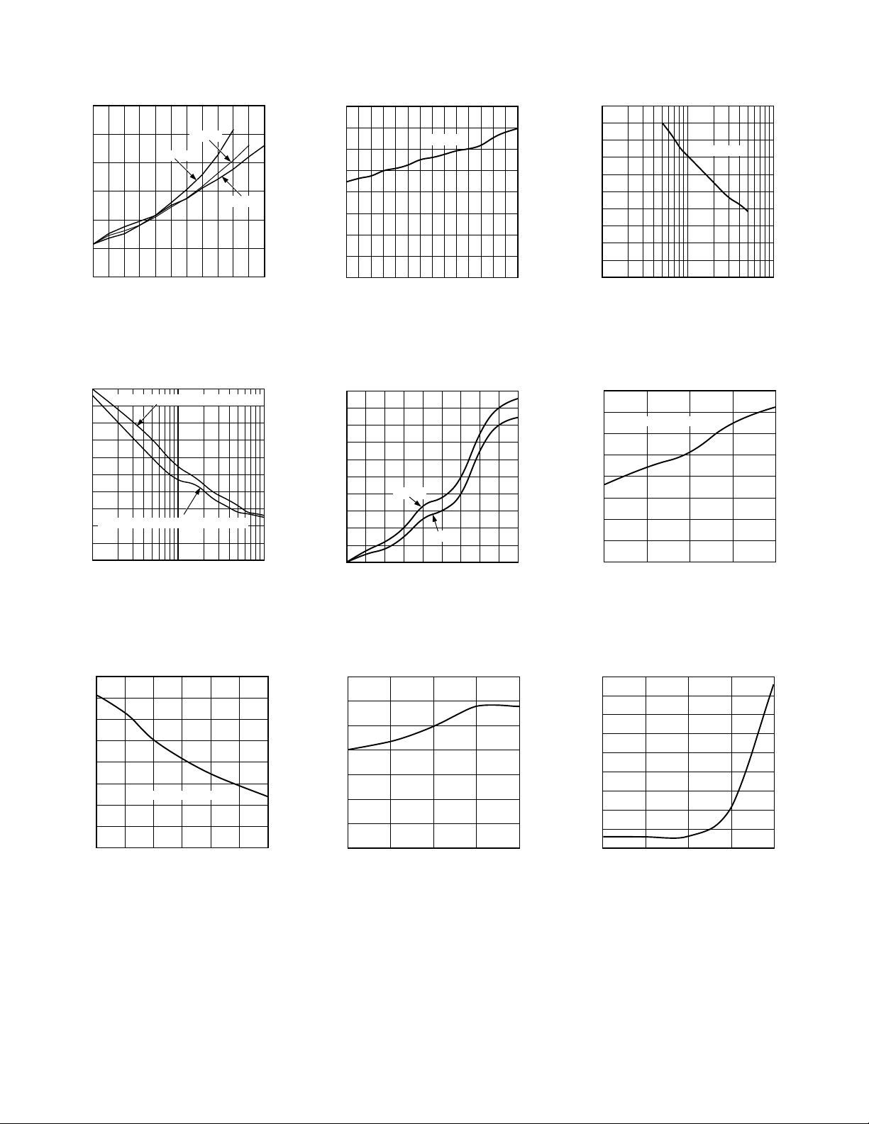
TEMPERATURE – °C
120
110
40
–40 0 8525 70
80
70
60
50
100
90
QUIESCENT CURRENT – µA
QUIESCENT CURRENT
–Typical Performance Characteristics
1.2
1.0
0.8
0.6
(SAT) – V
CE
V
0.4
0.2
0
0.2 1.20.4 0.6 0.8 1.0
SWITCH CURRENT – A
VIN = 3V
VIN = 2V
VIN = 5V
Figure 2. Saturation Voltage vs.
Switch Current in Step-Up Mode
1000
VIN =24V WITH L = 500µH @ V
900
800
700
600
500
400
300
SWITCH CURRENT – mA
VIN =12V WITH L = 250µH @ V
200
100
0
100 1000
R
– Ω
LIM
OUT
OUT
= 5V
= 5V
1.6
1.4
1.2
1.0
0.8
0.6
0.4
SWITCH ON VOLTAGE – V
0.2
0.0
0.15 0.25 0.35 0.45 0.55 0.65
0.05
V
CE(SAT)
SWITCH CURRENT – A
0.75
Figure 3. Switch ON Voltage vs.
Switch Current in Step-Down Mode
100
90
80
70
60
50
40
30
SUPPLY CURRENT – mA
20
10
0
0 100 900
VIN = 5V
VIN = 2V
200 300 400 600 700 800500
SWITCH CURRENT – mA
1100
1000
900
800
700
600
500
400
SWITCH CURRENT – mA
300
200
100
10 100 1000
2V < VIN < 5V
R
– Ω
LIM
Figure 4. Maximum Switch Current
vs. R
in Step-Up Mode
LIM
Figure 5. Maximum Switch Current
vs. R
in Step-Down Mode
LIM
25.5
25
24.5
24
23.5
23
22.5
OSCILLATOR FREQUENCY – kHz
22
21.5
OSCILLATOR FREQUENCY
35 30
10 15
INPUT VOLTAGE – Volts
Figure 8. Oscillator Frequency vs.
Input Voltage
20 25
Figure 6. Supply Current vs.
Switch Current
80
70
60
50
40
30
SET PIN BIAS CURRENT – nA
20
10
–40 0 85
TEMPERATURE – °C
V
= 3V
IN
25 70
Figure 9. Set Pin Bias Current vs.
Temperature
–4–
Figure 7. Quiescent Current vs.
Temperature
450
400
350
300
250
200
150
100
50
FEEDBACK PIN BIAS CURRENT – nA
0
–40 0 85
TEMPERATURE – °C
= 3V
V
IN
25 70
Figure 10. Feedback Pin Bias Current
vs. Temperature
REV. 0
Page 5

ADP1173
APPLICATIONS
Theory of Operation
The ADP1173 is a flexible, low power switch mode power
supply (SMPS) controller. The regulated output voltage can be
greater than the input voltage (boost or step-up mode) or less
than the input (buck or step-down mode). This device uses a
gated-oscillator technique to provide very high performance
with low quiescent current.
A functional block diagram of the ADP1173 is shown on the
front page. The internal 1.245 V reference is connected to one
input of the comparator, while the other input is externally
connected (via the FB pin) to a feedback network connected to
the regulated output. When the voltage at the FB pin falls below
1.245 V, the 24 kHz oscillator turns on. A driver amplifier provides base drive to the internal power switch, and the switching
action raises the output voltage. When the voltage at the FB pin
exceeds 1.245 V, the oscillator is shut off. While the oscillator is
off, the ADP1173 quiescent current is only 110 µA. The com-
parator includes a small amount of hysteresis, which ensures
loop stability without requiring external components for frequency compensation.
The maximum current in the internal power switch can be set
by connecting a resistor between V
and the I
IN
pin. When the
LIM
maximum current is exceeded, the switch is turned OFF. The
current limit circuitry has a time delay of about 2 µs. If an
external resistor is not used, connect I
information on I
is included in the Limiting the Switch
LIM
to VIN. Further
LIM
Current section of this data sheet.
The ADP1173 internal oscillator provides 23 µs ON and 19 µs
OFF times, which is ideal for applications where the ratio
between V
and V
IN
is roughly a factor of two (such as
OUT
converting +3 V to + 5 V). However, wider range conversions
(such as generating +12 V from a +5 V supply) can easily be
accomplished.
An uncommitted gain block on the ADP1173 can be connected
as a low battery detector. The inverting input of the gain block
is internally connected to the 1.245 V reference. The noninverting input is available at the SET pin. A resistor divider, connected between V
and GND with the junction connected to
IN
the SET pin, causes the AO output to go LOW when the low
battery set point is exceeded. The AO output is an open
collector NPN transistor which can sink 100 µA.
The ADP1173 provides external connections for both the
collector and emitter of its internal power switch, which permits
both step-up and step-down modes of operation. For the stepup mode, the emitter (pin SW2) is connected to GND and the
collector (pin SW1) drives the inductor. For step-down mode,
the emitter drives the inductor while the collector is connected
to V
.
IN
The output voltage of the ADP1173 is set with two external
resistors. Three fixed-voltage models are also available:
ADP1173-3.3 (+3.3 V), ADP1173-5 (+5 V) and ADP1173-12
(+12 V). The fixed-voltage models are identical to the ADP1173,
except that laser-trimmed voltage-setting resistors are included
on the chip. On the fixed-voltage models of the ADP1173,
simply connect the feedback pin (Pin 8) directly to the output
voltage.
COMPONENT SELECTION
General Notes on Inductor Selection
When the ADP1173 internal power switch turns on, current
begins to flow in the inductor. Energy is stored in the inductor
core while the switch is on, and this stored energy is then
transferred to the load when the switch turns off. Both the
collector and the emitter of the switch transistor are accessible
on the ADP1173, so the output voltage can be higher, lower or
of opposite polarity than the input voltage.
To specify an inductor for the ADP1173, the proper values of
inductance, saturation current and dc resistance must be
determined. This process is not difficult, and specific equations
for each circuit configuration are provided in this data sheet. In
general terms, however, the inductance value must be low
enough to store the required amount of energy (when both
input voltage and switch ON time are at a minimum) but high
enough that the inductor will not saturate when both V
IN
and
switch ON time are at their maximum values. The inductor
must also store enough energy to supply the load without
saturating. Finally, the dc resistance of the inductor should be
low, so that excessive power will not be wasted by heating the
windings. For most ADP1173 applications, an inductor of
47 µH to 470 µH, with a saturation current rating of 300 mA to
1 A and dc resistance <1 Ω is suitable. Ferrite core inductors
which meet these specifications are available in small, surfacemount packages.
To minimize Electro-Magnetic Interference (EMI), a toroid or
pot core type inductor is recommended. Rod core inductors are
a lower cost alternative if EMI is not a problem.
CALCULATING THE INDUCTOR VALUE
Selecting the proper inductor value is a simple three-step
process:
1. Define the operating parameters: minimum input voltage,
maximum input voltage, output voltage and output current.
2. Select the appropriate conversion topology (step-up, step-
down, or inverting).
3. Calculate the inductor value, using the equations in the
following sections.
Inductor Selection—Step-Up Converter
In a step-up, or boost, converter (Figure 14), the inductor must
store enough power to make up the difference between the
input voltage and the output voltage. The power that must be
stored is calculated from the equation:
P
where V
= V
()
L
OUT+VD–VIN(MIN )
is the diode forward voltage (≈ 0.5 V for a 1N5818
D
×I
()
OUT
(1)
Schottky). Energy is only stored in the inductor while the
ADP1173 switch is ON, so the energy stored in the inductor on
each switching cycle must be must be equal to or greater than:
P
L
f
OSC
(2)
in order for the ADP1173 to regulate the output voltage.
REV. 0
–5–
Page 6

ADP1173
When the internal power switch turns ON, current flow in the
inductor increases at the rate of:
IL(t)=
V
IN
R′
1–e
L
(3)
–R′t
where L is in henrys and R' is the sum of the switch equivalent
resistance (typically 0.8 Ω at +25°C) and the dc resistance of
the inductor. In most applications, where the voltage drop across
the switch is small compared to V
, a simpler equation can be
IN
used:
V
IL(t)=
IN
t
L
(4)
Replacing “t” in the above equation with the ON time of the
ADP1173 (23 µs, typical) will define the peak current for a
given inductor value and input voltage. At this point, the
inductor energy can be calculated as follows:
1
EL=
As previously mentioned, E
2
LI
PEAK
2
must be greater than PL/f
L
OSC
(5)
so the
ADP1173 can deliver the necessary power to the load. For best
efficiency, peak current should be limited to 1 A or less. Higher
switch currents will reduce efficiency, because of increased
saturation voltage in the switch. High peak current also increases
output ripple. As a general rule, keep peak current as low as possible to minimize losses in the switch, inductor and diode.
In practice, the inductor value is easily selected using the equations above. For example, consider a supply that will generate
9 V at 50 mA from a 3 V source. The inductor power required
is, from Equation 1:
PL=(9V +0.5V –3V)×(50 mA)=325mW
On each switching cycle, the inductor must supply:
P
325 mW
L
=
f
24 kHz
OSC
=13.5µJ
The required inductor power is fairly low in this example, so the
peak current can also be low. Assuming a peak current of 500 mA
as a starting point, Equation 4 can be rearranged to recommend
an inductor value:
L =
V
I
L(MAX )
IN
t =
500 mA
3V
23 µs =138 µH
Substituting a standard inductor value of 100 µH, with 0.2 Ω dc
resistance, will produce a peak switch current of:
–1.0Ω×23 µs
I
PEAK
=
3V
1. 0 Ω
1–e
100 µH
=616 mA
Once the peak current is known, the inductor energy can be
calculated from Equation 5:
1
EL=
(100 µH )×(616 mA)2=19 µJ
2
The inductor energy of 19 µJ is greater than the P
L/fOSC
re-
quirement of 13.5 µJ, so the 100 µH inductor will work in this
application. By substituting other inductor values into the same
equations, the optimum inductor value can be selected.
When selecting an inductor, the peak current must not exceed
the maximum switch current of 1.5 A. If the equations shown
above result in peak currents > 1.5 A, the ADP1073 should be
considered. This device has a 72% duty cycle, so more energy is
stored in the inductor on each cycle. This results in greater
output power.
The peak current must be evaluated for both minimum and
maximum values of input voltage. If the switch current is high
when V
ceeded at the maximum value of V
is at its minimum, then the 1.5 A limit may be ex-
IN
. In this case, the ADP1173’s
IN
current limit feature can be used to limit switch current. Simply
select a resistor (using Figure 4) that will limit the maximum
switch current to the I
value of V
stant I
. This will improve efficiency by producing a con-
IN
as VIN increases. See the Limiting the Switch Current
PEAK
value calculated for the minimum
PEAK
section of this data sheet for more information.
Note that the switch current limit feature does not protect the
circuit if the output is shorted to ground. In this case, current is
only limited by the dc resistance of the inductor and the forward
voltage of the diode.
Inductor Selection—Step-Down Converter
The step-down mode of operation is shown in Figure 15. Unlike
the step-up mode, the ADP1173’s power switch does not
saturate when operating in the step-down mode. Therefore,
switch current should be limited to 650 mA in this mode. If the
input voltage will vary over a wide range, the I
pin can be
LIM
used to limit the maximum switch current. If higher output
current is required, the ADP1111 should be considered.
The first step in selecting the step-down inductor is to calculate
the peak switch current as follows:
I
PEAK
OUT
VIN–VSW+V
V
OUT+VD
2I
=
DC
D
(6)
where DC = duty cycle (0.55 for the ADP1173)
V
= voltage drop across the switch
SW
V
= diode drop (0.5 V for a 1N5818)
D
I
= output current
OUT
V
= the output voltage
OUT
V
= the minimum input voltage
IN
As previously mentioned, the switch voltage is higher in stepdown mode than step-up mode. V
current and is therefore a function of V
For most applications, a V
value of 1.5 V is recommended.
SW
is a function of switch
SW
, L, time and V
IN
OUT
.
The inductor value can now be calculated:
V
IN(MIN )–VSW–VOUT
where t
L =
ON
I
PEAK
= switch ON time (23 µs)
×t
ON
(7)
If the input voltage will vary (such as an application that must
operate from a 12 V to 24 V source) an R
selected from Figure 5. The R
resistor will keep switch cur-
LIM
resistor should be
LIM
rent constant as the input voltage rises. Note that there are separate
R
values for step-up and step-down modes of operation.
LIM
–6–
REV. 0
Page 7

ADP1173
For example, assume that +5 V at 300 mA is required from a
12 V to +24 V input. Deriving the peak current from Equation 6
yields:
I
PEAK
2×300 mA
=
0.55
5 +0.5
12 –1.5+0.5
=545mA
The peak current can then be inserted into Equation 7 to calculate the inductor value:
12 –1.5– 5
L =
545 mA
×23 µs =232 µH
Since 232 µH is not a standard value, the next lower standard
value of 220 µH would be specified.
To avoid exceeding the maximum switch current when the
input voltage is at +24 V, an R
resistor should be specified.
LIM
Using the step-down curve of Figure 5, a value of 180 Ω will
limit the switch current to 600 mA.
Inductor Selection—Positive-to-Negative Converter
The configuration for a positive-to-negative converter using the
ADP1173 is shown in Figure 17. As with the step-up converter,
all of the output power for the inverting circuit must be supplied
by the inductor. The required inductor power is derived from
the formula:
PL= |V
|+V
()
OUT
×I
()
D
OUT
(8)
The ADP1173 power switch does not saturate in positive-tonegative mode. The voltage drop across the switch can be
modeled as a 0.75 V base-emitter diode in series with a 0.65 Ω
resistor. When the switch turns on, inductor current will rise at
a rate determined by:
_R't
1–e
L
L(DC)
(9)
V
IL(t)=
L
R'
where R' = 0.65 Ω + R
where VL = VIN – 0.75 V
For example, assume that a –5 V output at 50 mA is to be
generated from a +4.5 V to +5.5 V source. The power in the
inductor is calculated from Equation 8:
PL= |−5V|+0.5V
()
×(50 mA)= 275 mW
During each switching cycle, the inductor must supply the
following energy:
P
275 mW
L
=
f
24 kHz
OSC
=11.5µJ
Using a standard inductor value of 220 µH, with 0.2 Ω dc
resistance, will produce a peak switch current of:
–0.85 Ω×23 µs
I
PEAK
4.5V –0.75V
=
0.65 Ω+0.2 Ω
1–e
220 µH
=375mA
Once the peak current is known, the inductor energy can be
calculated from Equation 5:
1
EL=
(220 µH) ×(375 mA)2=15.5µJ
2
The inductor energy of 15.5 µJ is greater than the P
L/fOSC
requirement of 11.5 µJ, so the 220 µH inductor will work in
this application.
The input voltage only varies between 4.5 V and 5.5 V in this
example. Therefore, the peak current will not change enough to
require an R
directly to V
resistor and the I
LIM
. Care should be taken to ensure that the peak
IN
pin can be connected
LIM
current does not exceed 650 mA.
CAPACITOR SELECTION
For optimum performance, the ADP1173’s output capacitor
must be carefully selected. Choosing an inappropriate capacitor
can result in low efficiency and/or high output ripple.
Ordinary aluminum electrolytic capacitors are inexpensive, but
often have poor Equivalent Series Resistance (ESR) and
Equivalent Series Inductance (ESL). Low ESR aluminum capacitors, specifically designed for switch mode converter applications, are also available, and these are a better choice than
general purpose devices. Even better performance can be
achieved with tantalum capacitors, although their cost is higher.
Very low values of ESR can be achieved by using OS-CON*
capacitors (Sanyo Corporation, San Diego, CA). These devices
are fairly small, available with tape-and-reel packaging, and have
very low ESR.
The effects of capacitor selection on output ripple are demonstrated in Figures 11, 12, and 13. These figures show the output
of the same ADP1173 converter, which was evaluated with
three different output capacitors. In each case, the peak switch
current is 500 mA and the capacitor value is 100 µF. Figure 11
shows a Panasonic HF-series* radial aluminum electrolytic.
When the switch turns off, the output voltage jumps by about
90 mV and then decays as the inductor discharges into the
capacitor. The rise in voltage indicates an ESR of about
0.18 Ω. In Figure 12, the aluminum electrolytic has been
replaced by a Sprague 593D-series* tantalum device. In this
case the output jumps about 35 mV, which indicates an ESR of
0.07 Ω. Figure 13 shows an OS-CON SA series capacitor in the
same circuit, and ESR is only 0.02 Ω.
REV. 0
*All trademarks are properties of their respective holders.
–7–
Page 8

ADP1173
Figure 11. Aluminum Electrolytic
Figure 12. Tantalum Electrolytic
DIODE SELECTION
In specifying a diode, consideration must be given to speed,
forward voltage drop and reverse leakage current. When the
ADP1173 switch turns off, the diode must turn on rapidly if
high efficiency is to be maintained. Schottky rectifiers, as well as
fast signal diodes such as the 1N4148, are appropriate. The
forward voltage of the diode represents power that is not delivered to the load, so V
must also be minimized. Again, Schottky
F
diodes are recommended. Leakage current is especially important in low current applications, where the leakage can be a
significant percentage of the total quiescent current.
For most circuits, the 1N5818 is a suitable companion to the
ADP1173. This diode has a V
of 0.5 V at 1 A, 4 µA to 10 µA
F
leakage, and fast turn-on and turn-off times. A surface mount
version, the MBRS130T3, is also available. For applications
where the ADP1173 is “off” most of the time, such as when the
load is intermittent, a silicon diode may provide higher overall
efficiency due to lower leakage. For example, the 1N4933 has a
1 A capability, but with a leakage current of less than 1 µA. The
higher forward voltage of the 1N4933 reduces efficiency when
the ADP1173 delivers power, but the lower leakage may outweigh
the reduction in efficiency.
For switch currents of 100 mA or less, a Schottky diode such as
the BAT85 provides a V
of 0.8 V at 100 mA and leakage less
F
than 1 µA. A similar device, the BAT54, is available in a SOT23
package. Even lower leakage, in the 1 nA to 5 nA range, can be
obtained with a 1N4148 signal diode.
General purpose rectifiers, such as the 1N4001, are not suitable
for ADP1173 circuits. These devices, which have turn-on times
of 10 µs or more, are too slow for switching power supply
applications. Using such a diode “just to get started” will result
in wasted time and effort. Even if an ADP1173 circuit appears
to function with a 1N4001, the resulting performance will not
be indicative of the circuit performance when the correct diode
is used.
Figure 13. OS-CON Capacitor
If low output ripple is important, the user should consider the
ADP3000. This device switches at 400 kHz, and the higher
switching frequency simplifies the design of the output filter.
Consult the ADP3000 data sheet for additional details.
All potential current paths must be considered when analyzing
very low power applications, and this includes capacitor leakage
current. OS-CON capacitors have leakage in the 5 µA to 10 µA
range, which will reduce efficiency when the load is also in the
microampere range. Tantalum capacitors, with typical leakage
in the 1 µA to 5 µA range, are recommended for very low power
applications.
–8–
CIRCUIT OPERATION, STEP-UP (BOOST) MODE
In boost mode, the ADP1173 produces an output voltage that
is higher than the input voltage. For example, +12 V can be
generated from a +5 V logic power supply or +5 V can be
derived from two alkaline cells (+3 V).
Figure 16 shows an ADP1173 configured for step-up operation.
The collector of the internal power switch is connected to the
output side of the inductor, while the emitter is connected to
GND. When the switch turns on, pin SW1 is pulled near ground.
This action forces a voltage across L1 equal to V
IN–VCE(SAT),
and current begins to flow through L1. This current reaches a
final value (ignoring second-order effects) of:
V
I
PEAK
IN–VCE(SAT )
≅
L
×23 µs
where 23 µs is the ADP1173 switch’s “on” time.
REV. 0
Page 9

ADP1173
V
IN
I
* = OPTIONAL
R3*
2
1
LIMVIN
ADP1173
SW2GND
5
4
L1 D1
3
SW1
FB
8
R1
R2
V
OUT
+
C1
Figure 14. Step-Up Mode Operation
When the switch turns off, the magnetic field collapses. The
polarity across the inductor changes, current begins to flow
through D1 into the load and the output voltage is driven above
the input voltage.
The output voltage is fed back to the ADP1173 via resistors R1
and R2. When the voltage at pin FB falls below 1.245 V, SW1
turns “on” again and the cycle repeats. The output voltage is
therefore set by the formula:
V
=1.245 V × 1+
OUT
R1
R2
The circuit of Figure 14 shows a direct current path from VIN to
V
, via the inductor and D1. Therefore, the boost converter
OUT
is not protected if the output is short circuited to ground.
When the switch turns off, the magnetic field collapses. The
polarity across the inductor changes and the switch side of the
inductor is driven below ground. Schottky diode D1 then turns
on and current flows into the load. Notice that the Absolute
Maximum Rating for the ADP1173’s SW2 pin is 0.5 V below
ground. To avoid exceeding this limit, D1 must be a Schottky
diode. Using a silicon diode in this application will generate
forward voltages above 0.5 V, which will cause potentially
damaging power dissipation within the ADP1173.
The output voltage of the buck regulator is fed back to the
ADP1173’s FB pin by resistors R1 and R2. When the voltage at
pin FB falls below 1.245 V, the internal power switch turns
“on” again and the cycle repeats. The output voltage is set by
the formula:
V
OUT
=1.245 V × 1+
R1
R2
When operating the ADP1173 in step-down mode, the output
voltage is impressed across the internal power switch’s emitterbase junction when the switch is off. To protect the switch, the
output voltage should be limited to 6.2 V or less. If a higher
output voltage is required, a Schottky diode should be placed in
series with SW2, as shown in Figure 16.
If high output current is required in a step-down converter, the
ADP1111 or ADP3000 should be considered. These devices
offer higher frequency operation, which reduces inductor size,
and an external pass transistor can be added to reduce R
ON
of
the switch.
CIRCUIT OPERATION, STEP-DOWN (BUCK) MODE
The ADP1173’s step-down mode is used to produce an output
voltage lower than the input voltage. For example, the output of
four NiCd cells (+4.8 V) can be converted to a +3.3 V logic
supply.
A typical configuration for step-down operation of the ADP1173
is shown in Figure 15. In this case, the collector of the internal
power switch is connected to V
and the emitter drives the
IN
inductor. When the switch turns on, SW2 is pulled up toward
V
. This forces a voltage across L1 equal to (VIN–VCE) – V
IN
OUT
,
and causes current to flow in L1. This current reaches a final
value of:
V
I
PEAK
IN–VCE–VOUT
≅
L
×23 µs
where 23 µs is the ADP1173 switch’s “on” time.
V
IN
R3
100Ω
+
C2
1
I
LIMVIN
ADP1173
2
GND
3
SW1
8
FB
SW2
5
L1
4
+
D1
1N5818
C1
V
OUT
R1
R2
Figure 15. Step-Down Mode Operation
V
IN
R
LIM
100Ω
+
C2
1
I
LIMVIN
ADP1173
2
GND
3
SW1
8
FB
1N5818
SW2
4
5
L1
D1
1N5818
Figure 16. Step-Down Mode, V
+
OUT
C1
> 6.2 V
V
OUT
R1
R2
If the input voltage to the ADP1173 varies over a wide range, a
current limiting resistor at Pin 1 may be required. If a particular
circuit requires high peak inductor current with minimum input
supply voltage, the peak current may exceed the switch maximum rating and/or saturate the inductor when the supply
voltage is at the maximum value. See the Limiting the Switch
Current section of this data sheet for specific recommendations.
POSITIVE-TO-NEGATIVE CONVERSION
The ADP1173 can convert a positive input voltage to a negative
output voltage, as shown in Figure 17. This circuit is essentially
identical to the step-down application of Figure 15, except that
the “output” side of the inductor is connected to power ground.
When the ADP1173’s internal power switch turns off, current
flowing in the inductor forces the output (–V
) to a negative
OUT
potential. The ADP1173 will continue to turn the switch on
REV. 0
–9–
Page 10

ADP1173
until its FB pin is 1.245 V above its GND pin, so the output
voltage is determined by the formula:
+V
IN
C2
–V
OUT
+
=1.245 V × 1+
R3
2
1
I
LIMVIN
ADP1173
GND
5
SW1
R1
R2
3
8
FB
SW2
L1
4
D1
1N5818
+
R1
C1
R2
–V
OUT
Figure 17. A Positive-to-Negative Converter
The design criteria for the step-down application also apply to
the positive-to-negative converter. The output voltage should be
limited to |6.2 V|, unless a diode is inserted in series with the
SW2 Pin (see Figure 16). Also, D1 must again be a Schottky
diode to prevent excessive power dissipation in the ADP1173.
NEGATIVE-TO-POSITIVE CONVERSION
The circuit of Figure 18 converts a negative input voltage to a
positive output voltage. Operation of this circuit configuration is
similar to the step-up topology of Figure 14, except that the current
through feedback resistor R1 is level-shifted below ground by a
PNP transistor. The voltage across R1 is (V
OUT–VBEQ1
). However, diode D2 level-shifts the base of Q1 about 0.6 V below
ground, thereby cancelling the V
of Q1. The addition of D2
BE
also reduces the circuit’s output voltage sensitivity to temperature, which otherwise would be dominated by the –2 mV/°C V
BE
contribution of Q1. The output voltage for this circuit is determined by the formula:
V
OUT
=1.245 V ×
R1
R2
Unlike the positive step-up converter, the negative-to-positive
converter’s output voltage can be either higher or lower than the
input voltage.
LIMITING THE SWITCH CURRENT
The ADP1173’s R
pin permits the switch current to be lim-
LIM
ited with a single resistor. This current limiting action occurs on
a pulse by pulse basis. This feature allows the input voltage to
vary over a wide range, without saturating the inductor or exceeding the maximum switch rating. For example, a particular
design may require peak switch current of 800 mA with a 2.0 V
input. If V
rises to 4 V, however, the switch current will exceed
IN
1.6 A. The ADP1173 limits switch current to 1.5 A and thereby
protects the switch, but increases the output ripple. Selecting
the proper resistor will limit the switch current to 800 mA, even
if V
increases. The relationship between R
IN
and maximum
LIM
switch current is shown in Figures 4 and 5.
The I
feature is also valuable for controlling inductor current
LIM
when the ADP1173 goes into continuous-conduction mode. This
occurs in the step-up mode when the following condition is met:
V
OUT+VDIODE
VIN–V
SW
<
1– DC
1
where DC is the ADP1173’s duty cycle. When this relationship
exists, the inductor current does not go all the way to zero during the time the switch is OFF. When the switch turns on for
the next cycle, the inductor current begins to ramp up from the
residual level. If the switch ON time remains constant, the inductor current will increase to a high level (see Figure 19). This
increases output ripple, and can require a larger inductor and
capacitor. By controlling switch current with the I
resistor,
LIM
output ripple current can be maintained at the design values.
Figure 20 illustrates the action of the I
LIM
circuit.
1N5818
L1
D1
R
NEGATIVE
INPUT
LIM
2
1
+
I
C2
LIMVIN
ADP1173
SET
AO
6
7
NC NC
SW1
FB
SW2GND
4
5
R1
Q1
2N3906
3
8
R2
Figure 18. A Negative-to-Positive Converter
1N4148
D2
10kΩ
POSITIVE
OUTPUT
+
C
L
Figure 19. (I
Figure 20. (I
–10–
Operation, R
LIM
Operation, R
LIM
= 0 Ω)
LIM
= 240 Ω)
LIM
REV. 0
Page 11

ADP1173
2
V
IN
+5V
GND
ADP1173
R1
AO
SET
5
R2
100kΩ
TO
PROCESSOR
6
1.245V
REF
7
V
BAT
VLB –1.245V
12.5µA
VLB = BATTERY TRIP POINT
R2 = 100kΩ
R1 =
2
V
IN
5V
GND
ADP1173
R1
AO
SET
5
R2
47kΩ
TO
PROCESSOR
6
1.245mV
REF
7
V
BAT
R3
1.6MΩ
The internal structure of the I
circuit is shown in Figure 21.
LIM
Q1 is the ADP1173’s internal power switch, which is paralleled
by sense transistor Q2. The relative sizes of Q1 and Q2 are
scaled so that I
internal 80 Ω resistor and through the R
is 0.5% of IQ1. Current flows to Q2 through an
Q2
resistor. These two
LIM
resistors parallel the base-emitter junction of the oscillatordisable transistor, Q3. When the voltage across R1 and R
LIM
exceeds 0.6 V, Q3 turns on and terminates the output pulse. If
only the 80 Ω internal resistor is used (i.e., the I
nected directly to V
1.5 A. Figures 4 and 5 gives R
), the maximum switch current will be
IN
values for lower current-limit
LIM
pin is con-
LIM
values.
I
DRIVER
LIM
R1
80Ω
(INTERNAL)
Q2
SW1
Q1
SW2
V
IN
Q3
OSCILLATOR
R
LIM
(EXTERNAL)
Figure 21. Current Limit Operation
The delay through the current limiting circuit is approximately
2 µs. If the switch ON time is reduced to less than 4 µs, accu-
racy of the current trip-point is reduced. Attempting to program
a switch ON time of 2 µs or less will produce spurious responses
in the switch ON time. However, the ADP1173 will still provide
a properly regulated output voltage.
Figure 22. Setting the Low Battery Detector Trip Point
Figure 22 shows the gain block configured as a low battery
monitor. Resistors R1 and R2 should be set to high values to
reduce quiescent current, but not so high that bias current in the
SET input causes large errors. A value of 100 kΩ for R2 is a
good compromise. The value for R1 is then calculated from the
formula:
LOBATT
1.245 V
−1.245 V
R2
where V
V
R1=
is the desired low battery trip point. Since the
LOBATT
gain block output is an open-collector NPN, a pull-up resistor
should be connected to the positive logic power supply.
PROGRAMMING THE GAIN BLOCK
The gain block of the ADP1173 can be used as a low-battery
detector, error amplifier or linear post regulator. The gain block
consists of an op amp with PNP inputs and an open-collector
NPN output. The inverting input is internally connected to the
Figure 23. Adding Hysteresis to the Low Battery Detector
ADP1173’s 1.245 V reference, while the noninverting input is
available at the SET pin. The NPN output transistor will sink
about 100 µA.
REV. 0
–11–
Page 12

ADP1173
Typical Circuit Applications
L1*
68µH
R1
100Ω
2
1
I
2 x 1.5V
CELLS
*L1 = GOWANDA GA10-682K
COILTRONICS CTX68-4
FOR 5V INPUT CHANGE R1 TO 47Ω
CONVERTER WILL DELIVER –22V AT 40mA
LIMVIN
ADP1173
SW2GND
4
5
SW1
FB
1N5818
Figure 24. 3 V–22 V LCD Bias Generator
2
1
I
2 x 1.5V
CELLS
LIMVIN
ADP1173-5
SW2GND
4
5
3
8
L1*
82µH
SW1
SENSE
1N4148
4.7µF
3
8
2.21MΩ
1N5818
+
1%
1N5818
100µF
0.1µF
118kΩ
1%
220kΩ22µF
5V OUTPUT
150mA AT 3V INPUT
60mA AT 2V INPUT
–22V OUTPUT
7mA AT 2.0V INPUT
70% EFFICIENCY
BATTERY
100Ω
2
1
I
9V
LIMVIN
ADP1173-5
SW2GND
5
*L1 = GOWANDA GA10-472K
COILTRONICS CTX50-1
FOR HIGHER OUTPUT CURRENTS SEE ADP1073 DATASHEET
SENSE
4
SW1
1N5818
3
8
L1*
47µH
100µF
+
5V OUTPUT
150mA AT 9V INPUT
50mA AT 6.5V INPUT
Figure 27. 9 V to 5 V Converter
+V
IN
12V-28V
100Ω
2
1
I
LIMVIN
ADP1173-5
SW2GND
4
5
SW1
SENSE
1N5818
3
8
L1*
220µH
100µF
+
5V OUTPUT
300mA
*L1 = GOWANDA GA10-822K
Figure 25. 3 V to 5 V Step-Up Converter
+V
IN
5V INPUT
+
22µF
100Ω
2
1
I
LIMVIN
SW1
3
ADP1173-5
8
SENSE
GND
SW2
4
5
1N5818
*L1 = GOWANDA GA10-103K
COILTRONICS CTX100-1
L1*
100µH
Figure 26. +5 V to –5 V Converter
*L1 = GOWANDA GA10-223K
Figure 28. +20 V to 5 V Step-Down Converter
+
100µF
–5V OUTPUT
75mA
–12–
REV. 0
Page 13

ADP1173
48V DC
*L1 = CTX110077
I
4 x NICAD
ALKALINE
CELLS
44mH
44mH
= 120µA
Q
OR
~
~
470µF
L1*
100Ω
1
LIMVIN
ADP1173
SW2GND
5
500µH
1N4148
2
SW1
FB
4
+
+
47µF
100V
–
1N965B
10nF
3.6MΩ
10kΩ
15V
VN2222L
+
10µF
16V
12V
I
MUR110
+
220µF
10V
IRF530
3
8
390kΩ
2N5400
110kΩ
+5V
100mA
Figure 29. Telecom Supply
L1*
100µH 1N5818
56Ω
+
7
SET
2
1
I
LIMVIN
ADP1173
SW2GND
4
5
SW1
AO
3
6
FB
8
+
470µF
470kΩ
SI9405DY
240Ω
75k
V
= 5V AT 100mA
OUT
= 2.6V
AT V
IN
+
470µF
24kΩ
*L1 = GOWANDA GA20-103K
COILTRONICS CTX100-4
V
= 2.6V TO 7.2V
IN
Figure 30. 5 V to 5 V Step-Up or Step-Down Converter
470µF
+
2 x NICAD
47kΩ
100kΩ
2N3906
2.2MΩ
100kΩ
*L1 = COILTRONICS CTX-20-5-52
†
1% METAL FILM
100kΩ
6
7
1
I
LIMVIN
AO
ADP1173
SET
5
SW2GND
2
4
20µH, 5A
SW1
FB
L1*
3
8
100kΩ
220Ω
100Ω
†
301kΩ
2N4403
†
47Ω
1N5820
5Ω
MJE200
Figure 31. 2 V to 5 V at 200 mA Step-Up Converter with Undervoltage Lockout
+
+5V OUTPUT
200mA
LOCKOUT AT
1.85V INPUT
470µF
REV. 0
–13–
Page 14

ADP1173
L1*
51Ω
39kΩ
≤ 150µA
Q
25µH, 2A
1N5820
V
7V-24V
IN
0.22Ω
1
I
LIMVIN
ADP1173
GND
5
SW2
4
2
1N5818
SW1
FB
MTM20P08
18V
2kΩ
1W
3
100Ω
1/2W
8
V
IN
1N4148
2N3904
200kΩ
OP196
*L1 = GOWANDA GT10-100
EFFICIENCY ≥ 80% FOR 10mA ≤ I
STANDBY I
Figure 32. Voltage Controlled Positive-to-Negative Converter
L1*
V
7V-24V
0.22Ω
IN
1N5818
2
1
I
LIMVIN
SW1
ADP1173
SW2GND
4
5
18V
2kΩ
1W
3
100Ω
1/2W
FB
8
1N4148
MTM20P08
2N3904
40.2kΩ
25µH, 2A
1N5820
51Ω
121kΩ
+
470µF
= –5.13*V
–V
+
LOAD
470µF
OUT
VC (0V TO +5V)
≤ 500mA
5V
500mA
C
*L1 = GOWANDA GT10-100
OPERATE STANDBY
EFFICIENCY ≥ 80% FOR 10mA ≤ I
STANDBY I
≤ 150µA
Q
LOAD
≤ 500mA
Figure 33. High Power, Low Quiescent Current Step-Down Converter
–14–
REV. 0
Page 15

0.210 (5.33)
MAX
0.160 (4.06)
0.115 (2.93)
0.022 (0.558)
0.014 (0.356)
OUTLINE DIMENSIONS
Dimensions shown in inches and (mm).
8-Lead Plastic DIP
(N-8)
0.430 (10.92)
0.348 (8.84)
8
14
PIN 1
0.100
(2.54)
BSC
5
0.280 (7.11)
0.240 (6.10)
0.060 (1.52)
0.015 (0.38)
0.070 (1.77)
0.045 (1.15)
0.130
(3.30)
MIN
SEATING
PLANE
0.325 (8.25)
0.300 (7.62)
0.015 (0.381)
0.008 (0.204)
8-Lead Small Outline Package
(SO-8)
0.1968 (5.00)
0.1890 (4.80)
ADP1173
0.195 (4.95)
0.115 (2.93)
0.1574 (4.00)
0.1497 (3.80)
PIN 1
0.0098 (0.25)
0.0040 (0.10)
SEATING
PLANE
8
0.0500
(1.27)
BSC
5
0.2440 (6.20)
41
0.2284 (5.80)
0.0688 (1.75)
0.0532 (1.35)
0.0192 (0.49)
0.0138 (0.35)
0.0098 (0.25)
0.0075 (0.19)
0.0196 (0.50)
0.0099 (0.25)
8°
0°
0.0500 (1.27)
0.0160 (0.41)
x 45°
REV. 0
–15–
Page 16

C2965–12–1/97
–16–
PRINTED IN U.S.A.
 Loading...