

Page 1
High Efficiency Step-Down
a
FEATURES
Greater Than 95% Efficiency
Current Mode Switching Architecture Provides
Superior Load and Line Transient Response
Wide Input Voltage Range 3.5 V* to 16 V
User Defined Current Limit
Short Circuit Protection
Shutdown Pin
Low Dropout Voltage
Low Standby Current 160 mA typ
Low Cost
Available in 8-Lead PDIP or 8-Lead SOIC
APPLICATIONS
Portable Computers
Modems
Cellular Telephones
Portable Equipment
GPS Systems
Handheld Instruments
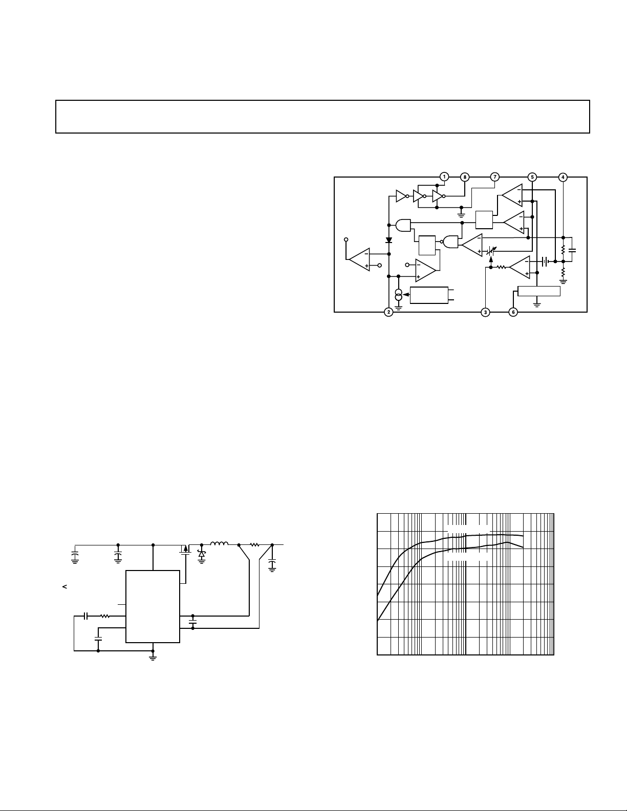
GENERAL DESCRIPTION
The ADP1147 is part of a family of High Efficiency Step-Down
Switching Regulators. These regulators offer superior load and
line transient response, a user defined current limit and an
automatic power savings mode. The automatic power savings
mode is used to maintain efficiency at lower output currents.
The ADP1147 incorporates a constant off-time, current mode
switching architecture to drive an external P-channel MOSFET
at frequencies up to 250 kHz. Constant off-time switching generates a constant ripple current in the external inductor. This
results in a wider input voltage operating range of 3.5 V* to
16 V, and a less complex circuit design.
*3.5 volt operation is for the ADP1147-3.3.
L
D1
30BQ040
1000pF
50mH
*
(5.2V TO 12V)
V
IN
+
1mF
0V = NORMAL
1.5V = SHUTDOWN
C
R
C
C
3300pF
1kV
C
T
470pF
+
C
IN
100mF
ADP1147
SHUTDOWN
I
TH
C
T
SHUTDOWN
V
IN
P-DRIVE
SENSE(+)
SENSE(–)
GND
P-CHANNEL
IRF7204
*COILTRONICS CTX 50–2MP
**KRL SL-1-C1-0R050J
Figure 1. High Efficiency Step-Down Converter
(Typical Application)
R
SENSE
0.05V
**
V
OUT
5V/2A
+
C
OUT
390mF
Switching Regulator Controllers
ADP1147-3.3/ADP1147-5
FUNCTIONAL BLOCK DIAGRAM
V
P-DRIVE GROUND
IN
ADP1147
2
C
V
IN
SENSE(–)
Q
10mV to 150mV
ITHSHUTDOWN
SLEEP
1
Q R
S
V
V
S
TH2
TH1
T
OFF-TIME
CONTROL
C
T
A very low dropout voltage with excellent output regulation can
be obtained by minimizing the dc resistance of the Inductor, the
R
resistor, and the R
SENSE
of the P-MOSFET. The power
DS(ON)
savings mode conserves power by reducing switching losses at
lower output currents. When the output load current falls below
the minimum required for the continuous mode the ADP1147
will automatically switch to the power savings mode. It will remain
in this mode until the inductor requires additional current or the
sleep mode is entered. In sleep mode with no load the standby
power consumption of the device is reduced to 2.0 mW typical
at V
= 10 V.
IN
For designs requiring even greater efficiencies refer to the
ADP1148 data sheet.
100
95
90
85
80
75
EFFICIENCY – %
70
65
60
1 10k10 100 1k
VIN = 6 VOLTS
VIN = 10 VOLTS
LOAD CURRENT – mA
Figure 2. ADP1147-5 Typical Efficiency, Figure 1 Circuit
SENSE(+)
V
R
B
S
13kV
V
OS
G
1.25V
REFERENCE
SENSE(–)
5pF
100kV
REV. 0
Information furnished by Analog Devices is believed to be accurate and
reliable. However, no responsibility is assumed by Analog Devices for its
use, nor for any infringements of patents or other rights of third parties
which may result from its use. No license is granted by implication or
otherwise under any patent or patent rights of Analog Devices.
One Technology Way, P.O. Box 9106, Norwood, MA 02062-9106, U.S.A.
Tel: 781/329-4700 World Wide Web Site: http://www.analog.com
Fax: 781/326-8703 © Analog Devices, Inc., 1998
Page 2

ADP1147-3.3/ADP1147-5–SPECIFICA TIONS
ELECTRICAL CHARACTERISTICS
(08C ≤ TA ≤ +708C1, VIN = 10 V, V
= 0 V unless otherwise noted)
SHUTDOWN
ADP1147
Parameter Conditions V
REGULATED OUTPUT VOLTAGE V
ADP1147-3-3 I
ADP1147-5 I
OUTPUT VOLTAGE LINE REGULATION T
= 9 V V
IN
= 700 mA 3.23 3.33 3.43 V
LOAD
= 700 mA 4.90 5.05 5.20 V
LOAD
= +25°C ∆V
A
S
OUT
OUT
Min Typ Max Units
VIN = 7 V to 12 V,
I
= 50 mA –40 0 +40 mV
LOAD
OUTPUT VOLTAGE LOAD REGULATION
ADP1147-3.3 5 mA < I
ADP1147-5 5 mA < I
Sleep Mode Output Ripple TA = +25°C, I
INPUT DC SUPPLY CURRENT
2
TA = +25°C
< 2 A ∆V
LOAD
< 2 A 60 100 mV
LOAD
= 0 A 50 mV p-p
LOAD
Normal Mode 4 V < VIN < 16 V I
OUT
Q
40 65 mV
1.6 2.3 mA
Sleep Mode (ADP1147-3.3) 4 V < VIN < 16 V 160 250 µA
Sleep Mode (ADP1147-5) 4 V < VIN < 16 V 160 250 µA
Shutdown V
CURRENT SENSE THRESHOLD VOLTAGE
ADP1147-3.3 V
SHUTDOWN
SENSE
TA = +25°C10mV
V
SENSE
= 2.1 V, 4 V < V
(–) = V
(–) = V
+
100 mV (
OUT
–
100 mV (
OUT
< 16 V 10 22 µA
IN
Forced
)
Forced
)V5–V
120 150 170 mV
4
ADP1147-5 V
SENSE
(–) = V
TA = +25°C10mV
V
(–) = V
SENSE
SHUTDOWN PIN THRESHOLD TA = +25°CV
SHUTDOWN PIN INPUT CURRENT 0 V < V
SHUTDOWN
+
100 mV (
OUT
–
100 mV (
OUT
Forced
Forced
< 8 V, VIN = 16 V I
)
) 120 150 170 mV
6
6
0.6 0.8 2 V
1.2 5 µA
TA = +25°C
PIN DISCHARGE CURRENT TA = +25°C, V
C
T
V
SENSE
(–) = V
OFF-TIME CT = 390 pF, I
DRIVER OUTPUT TRANSITION TIMES
TA = +25°C
in Regulation, 50 70 90 µA
OUT
OUT, VOUT
LOAD
= 0 V I
= 700 mA t
2
OFF
210µA
456 µs
CL = 3000 pF (Pin 8) VIN = 6 V tr, tf 100 200 ns
NOTES
1
All limits at temperature extremes are guaranteed via correlation using standard Statistical Quality Control (SQC) methods.
2
Dynamic supply current is higher due to the gate charge being delivered at the switching frequency.
Specifications subject to change without notice.
ABSOLUTE MAXIMUM RATINGS
Input Supply Voltage (Pin 1) . . . . . . . . . . . . . . 16 V to –0.3 V
Continuous Output Current (Pin 8) . . . . . . . . . . . . . . 50 mA
Sense Voltages (Pins 4, 5) . . . . . . . . . . . . . . . . 10 V to –0.3 V
Operating Ambient Temperature Range . . . . . 0°C to +70°C
Extended Commercial Temperature Range . . –40°C to +85°C
Junction Temperature* . . . . . . . . . . . . . . . . . . . . . . . +150°C
Storage Temperature Range . . . . . . . . . . . . –65°C to +150°C
Lead Temperature (Soldering, 10 sec) . . . . . . . . . . . +300°C
*TJ is calculated from the ambient temperature, TA, and power dissipation, PD,
according to the following formulas: ADP1147AN-3.3, ADP1147AN-5: TJ = TA +
(PD × 110°C/W). ADP1147AR-3.3, ADP1147AR-5: TJ = TA+(PD × 150°C/W).
Model Voltage Description Option
ADP1147AN-3.3 3.3 V Plastic DIP N-8
ADP1147AR-3.3 3.3 V SOIC SO-8
ADP1147AN-5 5 V Plastic DIP N-8
ADP1147AR-5 5 V SOIC SO-8
ORDERING GUIDE
Output Package Package
–2–
REV. 0
Page 3
ADP1147-3.3/ADP1147-5
ELECTRICAL CHARACTERISTICS
(–408C ≤ T A ≤ +858C1, VIN = 10 V, unless otherwise noted)
ADP1147
Parameter Conditions V
REGULATED OUTPUT VOLTAGE V
ADP1147-3.3 I
ADP1147-5 I
= 9 V
IN
= 700 mA V
LOAD
= 700 mA 4.85 5.05 5.2 V
LOAD
S
OUT
Min Typ Max Units
3.17 3.33 3.4 V
INPUT DC SUPPLY CURRENT
Normal Mode 4 V < V
< 16 V I
IN
Q
1.6 2.6 mA
Sleep Mode (ADP1147-3.3) 4 V < VIN < 16 V 160 280 µA
Sleep Mode (ADP1147-5) 5 V < VIN < 16 V 160 280 µA
Shutdown V
SHUTDOWN
CURRENT SENSE THRESHOLD VOLTAGE
ADP1147-3.3 V
SENSE
TA = +25°C25mV
V
ADP1147-5 V
SENSE
SENSE
TA = +25°C25mV
V
SENSE
SHUTDOWN PIN THRESHOLD V
OFF-TIME CT = 390 pF, I
NOTES
1
All limits at temperature extremes are guaranteed via correlation using standard Statistical Quality Control (SQC) methods.
Specifications subject to change without notice.
= 2.1 V, 4 V < V
(–) = V
(–) = V
(–) = V
(–) = V
+
100 mV (Forced) V5–V
OUT
–
100 mV (
OUT
+
100 mV (
OUT
–
100 mV (
OUT
LOAD
< 16 V 10 28 µ A
IN
Forced
) 120 150 175 mV
Forced
)
Forced
) 120 150 175 mV
= 700 mA t
6
OFF
4
0.55 0.8 2 V
3.8 5 6 µs
PIN FUNCTION DESCRIPTIONS
Pin
No. Mnemonic Function
1V
2C
IN
T
Input Voltage.
External Capacitor Connection. This capacitor sets the operating frequency of the device. The frequency is
also dependent on the input voltage level.
3I
TH
Error Amplifier Decoupling Pin. Pin 3 voltage level causes the comparator current threshold to increase.
4 SENSE(–) This connects to internal resistive divider, which senses the output voltage. Pin 4 is also the (–) input for the
current comparator.
5 SENSE(+) This provides the + input to the current comparator. The offset between Pins 4 and 5 together with R
SENSE
establish the current trip threshold.
6 SHUTDOWN When this pin is pulled high, it keeps the MOSFET turned off. When the pin is pulled to ground, the
ADP1147 functions normally. This pin cannot be left floating.
7 GND Independent ground lines must be connected separately to (a) the negative pin of C
of the Schottky diode and the negative terminal of C
.
IN
and (b) the cathode
OUT
8 P-DRIVE Provides high current drive for the MOSFET. Voltage swing is from VIN to ground at this pin.
PIN CONFIGURATIONS
8-Lead Plastic DIP (N-8)
V
I
SENSE–
T
1
IN
ADP1147
C
2
T
TOP VIEW
3
TH
(Not to Scale)
4
= 1258C, uJA = 1108C/W
JMAX
P-DRIVE
8
GND
7
6
SHUTDOWN
SENSE+
5
8-Lead SOIC (SO-8)
V
1
IN
ADP1147
C
2
T
TOP VIEW
(Not to Scale)
I
3
TH
SENSE–
4
T
= 1258C, uJA = 1508C/W
JMAX
P-DRIVE
8
GND
7
6
SHUTDOWN
5
SENSE+
CAUTION
ESD (electrostatic discharge) sensitive device. Electrostatic charges as high as 4000 V readily
accumulate on the human body and test equipment and can discharge without detection.
Although the ADP1147 features proprietary ESD protection circuitry, permanent damage may
occur on devices subjected to high energy electrostatic discharges. Therefore, proper ESD
precautions are recommended to avoid performance degradation or loss of functionality.
–3–REV. 0
WARNING!
ESD SENSITIVE DEVICE
Page 4
ADP1147-3.3/ADP1147-5
–Performance Characteristics
200
150
100
– mV
SENSE
R
50
0
051234
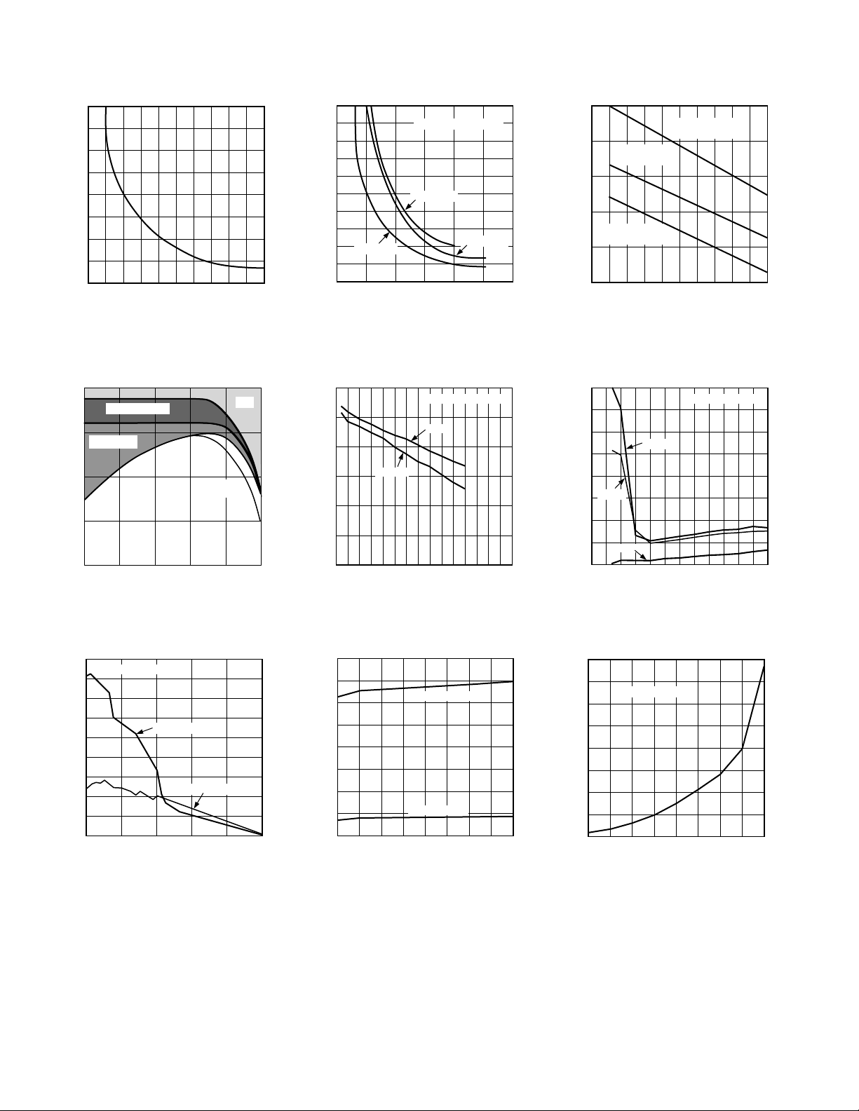
MAXIMUM OUTPUT CURRENT – Amps
Figure 3. Selecting R
SENSE
vs.
Maximum Output Current
100
GATE CHARGE
95
ADP1147 I
Q
90
EFFICIENCY – %
85
80
10m 30m 30.1 0.3 1
I
OUT
– Amps
SCHOTTKY
DIODE
I2R
Figure 6. Typical Efficiency Losses
1000
V
= V
= +5V
OUT
VIN = +10V
800
600
VIN = +12V
400
CAPACITANCE – pF
200
VIN = +7V
0
0 300100 200
FREQUENCY – kHz
SENSE
Figure 4. Operating Frequency vs.
Timing Capacitor
100
95
90
85
80
EFFICIENCY – %
75
70
0.1 AMP
58 2011 14 17
INPUT VOLTAGE – Volts
FIGURE 1 CIRCUIT
1 AMP
Figure 7. Efficiency vs. Input Voltage
1000
L = 50mH
R
= 0.02V
= 0.02V
= 0.05V
) VOLTAGE – Volts
OUT
SENSE
800
L = 25mH
R
SENSE
600
– mF
OUT
400
C
L = 50mH
R
SENSE
200
0
051 234
(VIN – V
Figure 5. Selecting Minimum Output
– V
Capacitor vs. (V
5.11
5.10
5.09
5.08
5.07
300mA
5.06
OUTPUT VOLTAGE – V
5.05
5.04
1 AMP
5.03
48 1612
IN
100mA
INPUT VOLTAGE – V
) and Inductor
OUT
FIGURE 1 CIRCUIT
Figure 8. ADP1147-5 Output Voltage
vs. Input Voltage
5.11
FIGURE 1 CIRCUIT
5.10
5.09
5.08
5.07
5.06
5.05
OUTPUT VOLTAGE – V
5.04
5.03
5.02
0 400 2000800 1200 1600
VIN = 6 VOLTS
VIN = 12 VOLTS
LOAD CURRENT – mA
Figure 9. Load Regulation
1.6
1.4
1.2
1.0
0.8
0.6
0.4
SUPPLY CURRENT – mA
0.2
0
46 208 1012141618
ACTIVE MODE
SLEEP MODE
INPUT VOLTAGE – Volts
Figure 10. DC Supply Current
40
35
V
30
25
20
15
10
SUPPLY CURRENT – mA
5
0
46 208 1012141618
= +2V
SHUTDOWN
INPUT VOLTAGE – Volts
Figure 11. Supply Current in
Shutdown
–4–
REV. 0
Page 5

ADP1147-3.3/ADP1147-5
INPUT VOLTAGE – Volts
OUTPUT VOLTAGE – V
3.35
3.34
3.27
48 1612
3.31
3.30
3.28
3.29
3.33
3.32
300mA
100mA
1 AMP
1.8
1.6
1.4
1.2
1.0
0.8
0.6
0.4
NORMALIZED FREQUENCY
0.2
0
12 1246810
(VIN – V
+70°C
OUT
0°C
+25°C
) – Volts
Figure 12. Operating Frequency vs.
(V
155
150
145
140
SENSE VOLTAGE – mV
135
IN–VOUT
)
MAXIMUM THRESHOLD
30
25
20
15
10
GATE CHARGE CURRENT – mA
QN + QP = 100nC
5
0
20 50 26080 110 140 170 200 230
QN + QP = 50nC
OPERATING FREQUENCY – kHz
Figure 13. Gate Charge Supply
Current
95
90
1 AMP
85
0.1 AMP
80
EFFICIENCY – %
75
80
70
60
50
+5V
40
30
OFF-TIME – ms
20
+3.3V
10
0
0.3 0.5 51 1.5 2 2.5 3 3.3 3.5 4 4.5
OUTPUT VOLTAGE – Volts
Figure 14. Off-Time vs. V
OUT
130
Figure 15. Current Sense Threshold
Voltage
3.36
3.34
3.32
3.30
3.28
3.26
3.24
OUTPUT VOLTAGE – V
3.22
3.20
3.18
Figure 18. Load Regulation (VO = 3.3 V);
Figure 1 Circuit with ADP1147-3.3
0 25 10070 85
0 400 2000800 1200 1600
TEMPERATURE – 8C
VIN = 6 VOLTS
VIN = 12 VOLTS
LOAD CURRENT – mA
70
58 2011 14 17
INPUT VOLTAGE – Volts
Figure 16. Efficiency vs. Input
Voltage at V
= 3.3 V; Figure 1
O
Circuit with ADP1147-3.3
–5–REV. 0
Figure 17. Output Voltage vs. Input
Voltage (V
= 3.3 V); Figure 1 Circuit
O
with ADP1147-3.3
Page 6

ADP1147-3.3/ADP1147-5
3.3V
0V
(a) Continuous Mode Operation
3.3V
0V
(b) Power Saving Mode
Figure 19. CT Waveforms
R
V
IN
C
390pF
T
3300pF
1kV
C
IN
ADP1147-3.3
V
IN
C
T
I
TH
P-CHANNEL
1mF
P-DRIVE
GROUND
SHUTDOWN
SENSE(+)SENSE(–)
1000pF
D1
SHUTDOWN
L
SENSE
V
OUT
C
OUT
GROUND
PLANE
Figure 20. Circuit Diagram Indicating the Recommended
Ground Plane Scheme for PCB Layout
V
IN
6V TO 14V
D1
1N4148
Q1
470pF
R7
2N3906
Q2
2N2222
D3
VN2222LL
Q3
R3
100V
R4
100V
220V
IRF7403
0.02V
R5
20kV
R6
470V
U1
P-DRV
2.2nF
GND
SHD
SNS+
C7
1N4148
8
7
6
5
C1
1mF
+
ADP1147-5
V
1
IN
2
C
C5
R1
1kV
C6
3.3nF
3
4
T
I
TH
SNS–
Q4
R2
C8
1mF
220mF/16V
OS-CON
D2
30BQ040
L1
50mH
C9–C11
220mF 3 10V
+
OS-CON
C2-C4
V
OUT
+
5V/3A
Figure 21. 5 V/3 A Regulator Using N-Channel Device
V
4V–14V
50mH
SENSE**
50mV
L*
IRF7204
D1
30BQ040
C
OUT
220mF
6.3V
X2
V
3.3V/2A
620pF
R
1kV
C
C
T
3300pF
ADP1147-3.3
V
IN
C
T
I
TH
SHUTDOWN
*COILTRONICS
CTX50-4
1mF
P-DRIVE
GND
SENSE(+)SENSE(–)
**KRL SL-1-C1-0R050J
SHUTDOWN
1nF
R
Figure 22. 3.3 V/2 A Regulator
100
95
90
85
80
75
EFFICIENCY – %
70
65
60
1 10K10
VIN = 6 VOLTS
VIN = 10 VOLTS
100 1K
LOAD CURRENT – mA
Figure 23. Efficiency vs. Load Current at VO = 3.3 V;
Figure 22 Circuit
IN
C
100mF
25V
OUT
IN
–6–
REV. 0
Page 7

ADP1147-3.3/ADP1147-5
APPLICATIONS
The ADP1147 family of regulators incorporate a current mode,
constant off-time architecture to switch an external P-channel
MOSFET. The external MOSFET can be switched at frequencies up to 250 kHz. The switching frequency of the device is
determined by the value selected for capacitor C
.
T
A regulated output voltage is maintained by the feedback voltage at the SENSE(–) pin. The SENSE(–) pin is connected to an
internal voltage divider. The voltage from this internal divider is
fed to comparator V, and gain block G. It is then compared to
an internal 1.25 volt reference.
The ADP1147 is capable of maintaining high levels of efficiency
by automatically switching between the power saving and continuous modes. The internal R-S flip-flop #2 controls the device
in the power saving mode, and gain block G assumes control
when the device is in the continuous mode of operation.
During the P-MOSFET on time, the voltage developed across
R
is monitored by the SENSE(–) and SENSE(+) pins of
SENSE
the device. When this voltage reaches the threshold level of
comparator C the output trips, switching the P drive to V
turns the external P-MOSFET off. At this point capacitor C
IN
, and
T
begins to discharge at a rate that is determined by the off-time
controller. The C
discharge current is proportional to the
T
voltage measured at the SENSE(–) pin. When the voltage on
cap C
decays to the threshold voltage (V
T
), comparator T
TH1
switches and sets R-S flip-flop #1. This forces the P-drive output low, and turns on the P-MOSFET. The sequence is then
repeated. As the load current is increased, the output voltage
starts to drop. This causes the gain circuit to raise the threshold
of the current comparator, and the load current is now tracked.
When load currents are low, comparator B sets the R-S flip-flop
#2 and asserts the power savings mode of operation. Comparator B monitors the voltage developed across R
. As the load
SENSE
current decreases to 50% of the designed inductor ripple current, the voltage reverses polarity. This reversal causes comparator B to trip, setting the Q-bar output of R-S flip-flop #2 to a
logic zero, and interrupts the cycle by cycle operation of the
output. The output storage capacitors are then slowly discharged
by the load. When the output cap voltage decays to the V
OS
level
of comparator V, it resets flip-flop #2, and the normal cycle by
cycle mode of operation resumes. If load currents are extremely
small, the time it takes for flip-flop #2 to reset increases. During
the extended wait for reset period, capacitor C
below the value of V
causing comparator S to trip. This
TH2
will discharge
T
forces the internal sleep bar low and the device enters the sleep
mode. A significant amount of the IC is disabled during the
sleep mode, reducing the ground current from 1.6 mA to
160 µA, typical. In sleep mode the P-MOSFET is turned off
until additional inductor current is required. The sleep mode is
terminated when flip-flop #2 is reset.
Due to the constant off-time architecture, the input voltage has
an effect on the device switching frequency. To limit the effects
of this variation in frequency the discharge current is increased
as the device approaches the dropout voltage of V
+1.5 V. In
IN
the dropout mode the P-MOSFET is constantly turned on.
Determining the Output Current and the Value for R
The value selected for R
is determined by the required
SENSE
SENSE
output current. The current comparator C has a threshold voltage range of 10 mV/R
to 150 mV/R
SENSE
maximum. This
SENSE
threshold sets the peak current in the external inductor and
yields a maximum output current of:
I
= I
MAX
The resistance values for R
–
PEAK
can range from 20 mΩ to
SENSE
200 mΩ. A graph for selecting R
I
SENSE
p−p
RIPPLE
2
vs. the maximum out-
put current is shown in Figure 3.
The value of R
can be determined by using the following
SENSE
equation:
R
(in mΩ) = 100/I
SENSE
MAX
This equation allows for a design margin due to component
variations.
The following equations are used to approximate the trip point
for the power savings mode and the peak short circuit current.
I
POWER SAVINGS
The ADP1147 automatically increases the t
I
SC(PK)
~ 5 mV/R
SENSE
= 150 mV/R
+ VO t
SENSE
/2L
OFF
time when a
OFF
short circuit condition is encountered. This allows sufficient
time for the inductor to decay between switching cycles. Due to
the resulting inductor ripple current the average short circuit
current I
is reduced to approximately I
SC(AVG)
MAX
.
Determining the Operating Frequency and Selecting Values
for C
and L
T
The ADP1147 incorporates a constant off-time architecture to
switch an external P-MOSFET. The off-time (t
mined by the value of the external timing cap C
P-MOSFET is turned on the voltage across C
) is deter-
OFF
. When the
T
is charged to
T
approximately 3.3 volts. During the switch off-time the voltage
on C
is discharged by a current that is proportional to the
T
voltage level of V
. The voltage across CT is representative of
OUT
the current in the inductor, which decays at a rate that is proportional to V
inductor must track the value selected for C
. Due to this relationship the value of the
OUT
.
T
The following equation is used to determine the desired continuous mode operating frequency:
V
OUT+VD
1−
CT=
VIN+V
1.3 × 10⁴× f
D
VD = the voltage drop across the Schottky diode.
The graph in Figure 4 can be used to help determine the capacitance value of C
vs. the operating frequency and input voltage.
T
The P-MOSFET gate charge losses increase with the operating
frequency and results in lower efficiency (see the Efficiency
section).
–7–REV. 0
Page 8

ADP1147-3.3/ADP1147-5
The formula used to calculate the continuous operating frequency is:
V
OUT+VD
1−
VIN+V
f =
t
=1.3 × 10⁴×CT×
OFF
V
is the value of the desired output voltage. V
REG
t
OFF
D
V
REG
V
OUT
is the ac-
OUT
tual measured value of the output voltage. When in regulation
V
REG/VOUT
is equal to 1. The switching frequency of the ADP1147
decreases as the input voltage decreases. The ADP1147 will
reduce the t
pacitor C
time by increasing the discharge current in ca-
OFF
if the input to output voltage differential falls below
T
1.5 volts. This is to eliminate the possible occurrence of audible
switching prior to dropout.
Now that the operating frequency has been determined and the
value selected for C
, the required inductance for inductor L
T
can be computed. The inductor L should be chosen so it will
generate no more than 25 mV/R
of peak-to-peak inductor
SENSE
ripple current.
The following equation is used to determine the required value
for inductor L:
25mV
R
SENSE
L
MIN
Substituting for t
(V
OUT+VD
=
(V
OUT+VD
=
above gives the minimum required induc-
OFF
L
MIN
25mV
)×t
)×t
OFF
or
OFF×RSENSE
tor value of:
L
= 5.1 × 10⁵× R
MIN
SENSE
× CT × V
REG
The ESR requirements for the output storage capacitor can be
relaxed by increasing the inductor value, but efficiency due to
copper losses will be reduced. Conversely, the use of too low an
inductance may allow the inductor current to become discontinuous, causing the device to enter the power savings mode
prematurely. As a result of this the power savings threshold is
lowered and the efficiency at lower current levels is severely
reduced.
Inductor Core Considerations
Now that the minimum inductance value for L has been determined, the inductor core selection can be made. High efficiency
converters generally cannot afford the core losses found in low
cost powdered iron cores. This forces the use of a more expensive ferrite, molypermalloy, or Kool Mu
®
cores. The typical
efficiency in Figure 1 reflects the use of a molypermalloy core.
The cost of the inductor can be cut in half by Using a Kool Mu
core type CTX 50-4 by Coiltronics, but the efficiency will be
approximately 1%–2% less. The actual core losses are not dependent on the size of the core, but on the amount of inductance. An increase in inductance will yield a decrease in the
amount of core loss. Although this appears to be desirable, more
inductance requires more turns of wire with added resistance
and greater copper losses.
Kool Mu is a registered trademark of Magnetics, Inc.
Using a ferrite cores in a design can produce very low core
losses, allowing the designer to focus on minimizing copper loss
and core saturation problems. Ferrite cores exhibit a condition
known as “Hard Saturation,” which results in an abrupt collapse
of the inductance when the peak design current is exceeded.
This causes the inductor ripple current to rise sharply, the output ripple voltage to increase and the power savings mode of
operation to be erroneously activated. To prevent this from
occurring the core should never be allowed to saturate.
Molypermalloy (from Magnetics, Inc.) is a very good, low loss
core material for a toroids, but is more expensive than a ferrite
core. A reasonable compromise between price and performance,
from the same manufacturer is Kool Mu. Toroidal cores are
extremely desirable where efficient use of available space and
several layers of wire are required. They are available in various
surface mount configurations from Coiltronics Inc. and other
companies.
Power MOSFET Selection and Considerations
The ADP1147 requires the use of an external P-channel
MOSFET. The major parameters to be considered when selecting the power MOSFET are the threshold voltage V
the on resistance of the device R
DS(ON)
.
GS(TH)
and
The minimum input voltage determines if the design requires a
logic level or a standard threshold MOSFET. In applications
where the input voltage is > 8 volts, a standard threshold
MOSFET with a V
where V
is < 8 volts, a logic level MOSFET with a V
IN
of < 4 volts can be used. In designs
GS(TH)
GS(TH)
of
< 2.5 volts is recommended. Note: If a logic level MOSFET
is selected, the supply voltage to the ADP1147 must not
exceed the absolute maximum for the V
of the MOSFET
GS
(e.g., < ± 8 volts for IRF7304).
The R
determined by the maximum output current (I
requirement for the selected power MOSFET is
DS(ON)
MAX
). An assumption is made that when the ADP1147 is operating in the
continuous mode, either the Schottky Diode or the MOSFET
are always conducting the average load current. The following
formulas are used to determine the duty cycle of each of the
components.
V
P−Channel MOSFET DutyCycle=
Schottky Diode Duty Cycle =
Once the Duty Cycle is known, the R
V
VIN+V
DS(ON)
IN–VD
OUT+VD
VIN+V
D
D
requirement for the
Power MOSFET can be determined by:
IN+VD
)×I
)×P
MAX
P
2
×(1+δP)
R
DS
(ON)
=
(V
OUT+VD
(V
where PP is the max allowable power dissipation and where δP is
the temperature dependency of R
ciency and thermal requirements will determine the value of P
for the MOSFET. Effi-
DS(ON)
,
P
(refer to Efficiency section). MOSFETS usually specify the 1+ δ
as a normalized R
vs. temperature trace, and δ can be
DS(ON )
approximated to 0.007/°C for most low voltage MOSFETs.
Output Diode Considerations
When selecting the output diode careful consideration should be
given to peak current and average power dissipation so the
maximum specifications for the diode are not exceeded.
–8–
REV. 0
Page 9

ADP1147-3.3/ADP1147-5
The Schottky diode is in conduction during the MOSFET offtime. A short circuit of V
= 0 is the most demanding situa-
OUT
tion on for the diode. During this time it must be capable of
delivering I
for duty cycles approaching 100%. The equa-
SC(PK)
tion below is used to calculate the average current conducted by
the diode under normal load conditions.
V
IN–VOUT
ID1=
VIN+V
×I
LOAD
D
To guard against increased power dissipation due to undesired
ringing, it is extremely important to adhere to the following:
1. Use proper grounding techniques.
2. Keep all track lengths as short as possible, especially connections made to the diode (refer to PCB Layout Considerations
section).
The allowable forward voltage drop of the diode is determined
by the maximum short circuit current and power dissipation.
The equation below is used to calculate V
= PD/I
V
F
SC(PK)
:
F
where PD is the maximum allowable power dissipation and is
determined by the system efficiency and thermal requirements
(refer to Efficiency Section).
C
Considerations
IN
During the continuous mode of operation the current drawn
from the source is a square wave with a duty cycle equal to
V
OUT/VIN
. To reduce or prevent large voltage transients an input
capacitor with a low ESR value and capable of handling the
maximum rms current should be selected. The formula below
is used to determine the required maximum rms capacitor
current:
C
IN IRMS = [VOUT
(VIN–V
The maximum for this formula is reached when VIN = 2 V
where I
RMS
= I
/2. It is best to use this worst case scenario for
OUT
OUT
0.5
)]
× I
MAX/VIN
,
OUT
design margin. Manufacturers of capacitors typically base the
current ratings of their caps on a 2000-hour life. This requires a
prudent designer to use capacitors that are derated or rated at a
higher temperature. The use of multiple capacitors in parallel
may also be used to meet design requirements. The capacitor
manufacturer should be consulted for questions regarding specific capacitor selection.
In addition, for high frequency decoupling a 0.1 µF to 1.0 µF
ceramic capacitor should be placed and connected as close to
the V
C
pin as possible.
IN
Considerations
OUT
The minimum required ESR value is the primary consideration
when selecting C
value of C
R
SENSE
OUT
(see equation below):
C
When selecting a capacitor for C
. For proper circuit operation the ESR
OUT
must be less than two times the value selected for
Minimum Required ESR < 2 R
OUT
, the minimum required
OUT
SENSE
ESR is the primary concern. Proper circuit operation mandates
that the ESR value of C
value of R
SENSE
.
A capacitor with an ESR value equal to R
best overall efficiency. If the ESR value of C
two times R
a 1% decrease in efficiency results. United
SENSE
must be less than two times the
OUT
will provide the
SENSE
increases to
OUT
Chemicon, Nichicon and Sprague are three manufacturers of
high grade capacitors. Sprague offers a capacitor that uses an
OS-CON semiconductor dielectric. This style capacitor provides the lowest amount of ESR for its size, but at a higher cost.
Most capacitors that meet the ESR requirements for I
ripple
P-P
will usually meet or exceed the rms current requirements. The
specifications for the selected capacitor should be consulted.
Surface mount applications may require the use of multiple
capacitors in parallel to meet the ESR or rms current requirements. If dry tantalum capacitors are used it is critical that they
be surge tested and recommended by the manufacturer for use
in switching power supplies such as Type 593D from Sprague.
AVX offers the TPS series of capacitors with various heights
from 2 mm to 4 mm. The manufacturer should be consulted
for the latest information, specifications and recommendations
concerning specific capacitors. When operating with low supply
voltages, a minimum output capacitance will be required to
prevent the device from operating in a low frequency mode (see
Figure 5). The output ripple also increases at low frequencies if
C
is too small.
OUT
Transient Response
The response of the regulator loop can be verified by monitoring
the transient load response. Several cycles may be required for a
switching regulator circuit to respond to a step change in the dc
load current (resistive load). When a step in the load current
takes place a change in V
in V
of I
C
is equal to the delta of I
OUT
charges or discharges the output voltage on capacitor
LOAD
. This continues until the regulator loop responds to the
OUT
change in load and is able to restore V
V
should be monitored during the step change in load for
OUT
occurs. The amount of the change
OUT
× ESR of C
LOAD
OUT
. The delta
OUT
to its original value.
overshoot, undershoot or ringing, which may indicate a stability
problem. The circuit shown in Figure 1 contains external components that should provide sufficient compensation for most
applications. The most demanding form of a transient that can
be placed on a switching regulator is the hot switching in of
loads that contain bypass or other sources of capacitance greater
than 1 µF. When a discharged capacitor is placed on the load it
is effectively placed in parallel with the output cap C
results in a rapid drop in the output voltage V
OUT
, and
OUT
. Switching
regulators are not capable of supplying enough instantaneous
current to prevent this from occurring. Therefore, the inrush
current to the load capacitors should be held below the current
limit of the design.
Efficiency
Efficiency is one of the most important reasons for choosing a
switching regulator. The percentile efficiency of a regulator can
be determined by dividing the output power of the device by the
input power and then multiplying the results by 100. Efficiency
losses can occur at any point in a circuit and it is important to
analyze the individual losses to determine changes that would
yield the most improvement. The efficiency of a circuit can be
expressed as:
% efficiency = 100% – (% L1 + % L2 + % L3... etc.)
L1, L2, L3, etc., are the individual losses as a percentage of the
input power. In high efficiency circuits small errors result when
expressing losses as a percentage of the output power.
–9–REV. 0
Page 10

ADP1147-3.3/ADP1147-5
Losses are encountered in all elements of the circuit, but the
four major sources for the circuit shown in Figure 1 are:
1. The ADP1147 dc bias current.
2. The MOSFET gate charge current.
2
3. The I
4. The voltage drop of the Schottky diode.
1. The ADP1147’s dc bias current is the amount of current that
2. The MOSFET gate charge current is due to the switching of
3. I
4. At high current loads the Schottky diode can be a substantial
× R losses.
flows into VIN of the device minus the gate charge current.
With V
= 10 volts, the dc supply current to the device is
IN
typically 160 µA for a no load condition, and increases pro-
portionally with load to a constant of 1.6 mA in the continuous mode of operation. Losses due to dc bias currents increase
as the input voltage V
is increased. At VIN = 10 volts the dc
IN
bias losses are usually less than 1% with a load current
greater than 30 mA. When very low load currents are
encountered the dc bias current becomes the primary point
of loss.
the power MOSFET’s gate capacitance. As the MOSFET’s
gate is switched from a low to a high and back to a low again,
charge impulses dQ travel from V
out of V
is equal to dQ/dt and is usually much greater than
IN
to ground. The current
IN
the dc supply current. When the device is operating in the
continuous mode the I gate charge is = f (Q
P-channel power MOSFET with an R
). Typically a
P
on of 135 mΩ will
DS
have a gate charge of 40 nC. With a 100 kHz, switching
frequency in the continuous mode, the I gate charge would
equate to 4 mA or about a 2%–3% loss with a V
of 10 volts.
IN
It should be noted that gate charge losses increase with
switching frequency or input voltage. A design requiring the
highest efficiency can be obtained by using more moderate
switching frequencies.
2
× R loss is a result of the combined dc circuit resistance
and the output load current. The primary contributors to
circuit dc resistance are the MOSFET, the Inductor and
R
. In the continuous mode of operation the average
SENSE
output current is switched between the MOSFET and the
Schottky diode and a continuous current flows through the
inductor and R
. Therefore the R
SENSE
of the MOSFET
DS(ON)
is multiplied by the on portion of the duty cycle. The result is
then combined with the resistance of the Inductor and
R
. The following equations and example show how to
SENSE
approximate the I
R
DS(ON)
With the duty cycle = 0.5, R
and I
= 0.5 A. The result would be a 3% I2R loss. The
LOAD
effects of I
2
× R losses of a circuit.
× (Duty Cycle) + R
I
LOAD
V
OUT
P
LOSS/POUT
2
R losses causes the efficiency to fall off at higher
× 100 = % I2 × R
2
× R = P
× I
LOAD
INDUCTOR
INDUCTOR
= P
LOSS
OUT
= 0.15, R
+ R
LOSS
SENSE
.
SENSE
= R
= 0.05
output currents.
point of power loss. The diode efficiency is further reduced
by the use of high input voltages. To calculate the diode loss,
the load current should be multiplied by the duty cycle of the
diode times the forward voltage drop of the diode.
I
× % duty cycle × V
LOAD
= Diode Loss
DROP
Figure 6 indicates the distribution of losses versus load current in a typical ADP1147 switching regulator circuit. With
medium current loads the gate charge current is responsible
for a substantial amount of efficiency loss. At lower loads the
gate charge losses become large in comparison to the load,
and result in unacceptable efficiency levels. When low load
currents are encountered the ADP1147 employs a power
savings mode to reduce the effects of the gate loss. In the
power savings mode of operation the dc supply current is the
major source of loss and becomes a greater percentage as the
output current decreases.
Losses at higher loads are primarily due to I
2
R and the
Schottky diode. All other variables such as capacitor ESR
dissipation, MOSFET switching, and inductor core losses
typically contribute less than 2% additional loss.
Circuit Design Example
In using the design example below assumptions are as follows:
= 5 Volts
V
IN
V
= 3.3 Volts
OUT
V
drop (VD) = 0.4 Volts
DIODE
I
MAX OUT
= 1 Amp
Max switching frequency (f) = 100 kHz.
The values for R
, CT and L can be calculated based on the
SENSE
above assumptions.
R
= 100 mV/1 Amp = 100 mΩ.
SENSE
t
time = (1/100 kHz) × [1 – (3.7/5.4)] = 3.15 µs.
OFF
C
= 3.15 µs /(1.3 × 10 4) = 242 pF.
T
L = 5.1 × 10
5
× 0.1 Ω × 242 pF × 3.3 V = 41 µH.
If we further assume:
1. The data is specified at +25°C.
2. MOSFET max power dissipation (P
) is limited to 250 mW.
P
3. MOSFET thermal resistance is 50°C/W.
4. The normalized R
vs. temperature approximation (δP)
DS(ON)
is 0.007/°C.
This results in 250 mW × 50°C per watt = 12.5°C of MOSFET
heat rise. If the ambient temperature T
temperature of 12.5°C +50°C, T
is 50°C, a junction
A
= 62.5°C. δP = 0.007 ×
A
(62.5°C –25°C) = 0.2625
We can now determine the required R
= 5(0.25)/3.3 (1)2 (1.2625) = 300 mΩ
R
DS(ON)
for the MOSFET:
DS(ON)
The above requirements can be met with the use of a P-channel
IRF7204 or an Si9430.
When V
is short circuited the power dissipation of the
OUT
Schottky diode is at worst case and the dissipation can rise
greatly. The following equation can be used to determine the
power dissipation:
P
A 100 mΩ R
= I
D
resistor will yield an I
SENSE
SC(AVG)
× V
DIODE
Drop
of 1 A. With a
SC(AVG)
forward diode drop of 0.4 volts a 400 milliwatt diode power
dissipation results.
The rms current rating needed for C
will be at least 0.5 A over
IN
the temperature range.
–10–
REV. 0
Page 11

ADP1147-3.3/ADP1147-5
To obtain optimum efficiency the required ESR value of C
OUT
is 100 mΩ or less.
The circuit should also be evaluated with the minimum input
voltage. This is done to assure that the power dissipation and
junction temperature of the P-channel MOSFET are not exceeded. At lower input voltages the operating frequency of the
ADP1147 decreases. This causes the P-channel MOSFET to
remain in conduction for longer periods of time, resulting in
more power dissipation in the MOSFET.
The effects of V
can be evaluated if we assume the
IN(MIN)
following:
V
V
V
f
Troubleshooting Hints
= 4.5 V
IN(MIN)
= 3.3 V
OUT
= 0.4 V
D
= (1/3.15 µs) × (1– (3.7/4.9)) = 78 kHz.
MIN
2
3.3(0.125Ω)(1 A)
PD=
(1.2625)
4.5
=116 mW
Efficiency is the primary reason for choosing the ADP1147 for
use in an application, and it is critical to determine that all portions of the circuit are functioning properly in all modes. After
the design is complete the voltage waveforms on the timing
capacitor, C
, at Pin 2 of the device, should be compared to the
T
waveforms in Figures 19a and 19b.
In the continuous mode of operation the dc voltage level of the
waveform on C
should never fall below the 2 V level and it
T
should have a 0.9 V peak-to-peak sawtooth on it (see Figure
19a).
In the Power Savings Mode the sawtooth waveform on C
will
T
decay to ground for extended periods of time (see Figure 19b).
During the time that the capacitor voltage is at ground the
ADP1147 is in the power savings or sleep mode and the quiescent current is reduced to 160 µA typical.
The ripple current in the inductor should also be monitored to
determine that it is approximately the same in both modes of
operation. With a higher output currents the voltage level on C
T
should never decay to ground as this would indicate poor
grounding and or decoupling.
Printed Wire Board Layout Considerations
The PWB layout is extremely critical for proper circuit operation and the items listed below should be carefully considered
(see Figure 20)
1. The signal and power grounds should be separate from each
other. They should be tied together only at ground Pin 7 of
the ADP1147. The power ground should be tied to the anode of the Schottky diode, and the (–) side of the C
capaci-
IN
tor. The connections should be made with traces that are as
wide and as short as possible. The signal ground should be
connected to the (–) side of capacitor C
using the same
OUT
type of runs as above.
2. The sense(–) run to Pin 4 of the ADP1147 should be connected directly to the junction point of R
of C
OUT
.
and the + side
SENSE
3. The sense(–) and sense(+) traces should be routed together
with minimum track spacing and run lengths. The 1000 pF
filter capacitor across Pins 4 and 5 of the ADP1147 should
be located as close to the device as possible.
4. In order to supply sufficient ac current the (+) side of capacitor C
should be connected with wide short traces and must
IN
be located as close to the source of the P-MOSFET as possible.
5. In order to supply high frequency peak currents the input
decoupling capacitors should range from 0.1 µF to 1.0 µF
and must be located as close to the V
pin and the ground
IN
Pin 7 as possible.
6. The shutdown Pin (6) is a high impedance input and it must
not be allowed to float. The normal mode of operation of the
device requires that this pin be pulled low.
–11–REV. 0
Page 12

ADP1147-3.3/ADP1147-5
0.210 (5.33)
MAX
0.160 (4.06)
0.115 (2.93)
0.022 (0.558)
0.014 (0.356)
OUTLINE DIMENSIONS
Dimensions shown in inches and (mm).
8-Lead Plastic DIP
(N-8)
0.430 (10.92)
0.348 (8.84)
8
14
PIN 1
0.100
(2.54)
BSC
5
0.280 (7.11)
0.240 (6.10)
0.060 (1.52)
0.015 (0.38)
0.070 (1.77)
0.045 (1.15)
0.130
(3.30)
MIN
SEATING
PLANE
0.325 (8.25)
0.300 (7.62)
0.015 (0.381)
0.008 (0.204)
8-Lead SOIC
(SO-8)
0.1968 (5.00)
0.1890 (4.80)
C3148–8–2/98
0.195 (4.95)
0.115 (2.93)
0.1574 (4.00)
0.1497 (3.80)
PIN 1
0.0098 (0.25)
0.0040 (0.10)
SEATING
PLANE
8
0.0500
(1.27)
BSC
5
0.2440 (6.20)
41
0.2284 (5.80)
0.0688 (1.75)
0.0532 (1.35)
0.0192 (0.49)
0.0138 (0.35)
0.0098 (0.25)
0.0075 (0.19)
0.0196 (0.50)
0.0099 (0.25)
8°
0°
0.0500 (1.27)
0.0160 (0.41)
x 45°
–12–
PRINTED IN U.S.A.
REV. 0
 Loading...