

Page 1

Digital Power Factor Correction Controller
Preliminary Technical Data
FEATURES
Flexible, single phase, digital power factor correction (PFC)
controller
True rms ac power metering
Enhanced dynamic response
Optimized light load efficiency performance
Output voltage adjustment
Frequency reduction
Inrush control
Switching frequency spread spectrum for improved EMI
External frequency synchronization
PMBus compliant
Programmable ac line fault detection and protection
Programmable output fault detection and protection
Extensive fault protection for high reliability systems
Frequency range from 30 kHz to 400 kHz
8 kB EEPROM
Programming via easy-to-use graphical user interface (GUI)
APPLICATIONS
AC/DC power supplies for applications including
Computing server and storage
Network and communication infrastructure
Industrial and medical
GENERAL DESCRIPTION
The ADP1047 is a digital power factor correction controller
providing accurate input power metering capability and inrush
control targeting ac/dc systems.
The digital PFC function is based on a conventional boost PFC
with multiplication of the output voltage feedback combined
with the input current and voltage to provide optimum harmonic
correction and power factor for ac/dc systems. All signals are
converted into the digital domain to provide maximum
With Accurate AC Power Metering
ADP1047
flexibility—all key parameters can be reported and adjusted via
the PMBus interface. This allows users to optimize system performance, maximize efficiency across the load range, and reduce
design time to market.
The ADP1047 provides accurate, rms measurement of input
voltage, current and power. This information can be reported
to the secondary of the power supply via the PMBus interface.
The combination of a flexible, digitally controlled PFC engine
and accurate input power metering facilitate the adoption of
intelligent power management systems capable of making decisions
to improve end user system efficiency. The device targets further
efficiency improvements through programmable frequency
reduction at light load and the capability to reduce the output
voltage at low loads.
The ADP1047 provides enhanced integrated features and
functions; the Inrush and soft start control functions provide
significant component count reduction with easy design
optimization.
The device targets high reliability, redundant power supply
applications and has extensive and robust protection circuitry:
independent overvoltage protection, overcurrent (ILIM), ground
continuity metering, and ac sensing. Internal overtemperature
is provided and external temperature can be recorded via an
external sensing device.
The internal 8 kB EEPROM stores all the programmed values
and allows standalone control without a microcontroller. All
parametric reporting and adjustments are programmed via an
easy-to-use GUI—no complex programming is required.
The ADP1047 operates from a single 3.3 V supply. The device is
available in a 24-lead QSOP package specified over ambient
temperature range −40°C to +85°C.
Rev. PrA
Information furnished by Analog Devices is believed to be accurate and reliable. However, no
responsibility is assumed by Anal og Devices for its use, nor for any infringements of patents or ot her
rights of third parties that may result from its use. Specifications subject to change without notice. No
license is granted by implication or otherwise under any patent or patent rights of Analog Devices.
Trademarks and registered trademarks are the property of their respective owners.
One Technology Way, P.O. Box 9106, Norwood, MA 02062-9106, U.S.A.
Tel: 781.329.4700 www.analog.com
Fax: 781.461.3113 ©2011 Analog Devices, Inc. All rights reserved.
Page 2

ADP1047 Preliminary Technical Data
TABLE OF CONTENTS
Features.............................................................................................. 1
Applications....................................................................................... 1
General Description ......................................................................... 1
Functional Block Diagram .............................................................. 3
Specifications..................................................................................... 4
Absolute Maximum Ratings ............................................................7
ESD Caution...................................................................................7
Pin Configuration And Function Descriptions ............................8
Theory of Operation .........................................................................9
Outline Dimensions....................................................................... 10
Rev. PrA | Page 2 of 12
Page 3
Preliminary Technical Data ADP1047
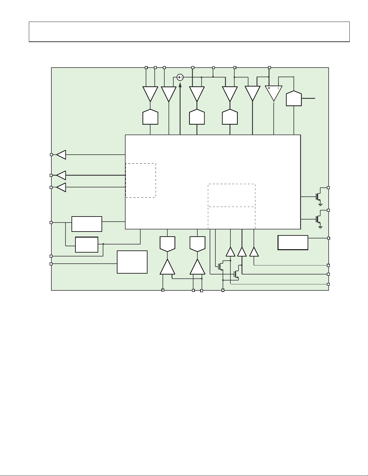
FUNCTIONAL BLOCK DIAGRAM
OVP
PGND
DAC
ADP1047
CS- CS+
ILIM
VAC PGND
VFB
INRUSH
PWM
PWM2
VDD
VCORE
RES
UVLO
LDO
PWM
ENGINE
VREF
ADC
CS
OCP
ADC
ADC
VAC
DIGITALCORE
8kb EEPROM
I2C
INTERFACE
ADC
ADC
VFB
OLP OVP
OSC
PGOOD
AC_OK
SYNC
PSON
SCL
SDA
ADD
RTD
Figure 1.
AGND
DGND
Rev. PrA | Page 3 of 12
Page 4

ADP1047 Preliminary Technical Data
SPECIFICATIONS
VDD = 3.3 V TA = -40°C to +85°C, unless otherwise noted.
Table 1.
Parameter Symbol Test Conditions/Comments Min Typ Max Units
POWER SUPPLY
Operating Supply Voltage VDD 3.0 3.3 3.6 V
Supply Current IDD Normal operation (PSON high) 17 mA
Peak Supply Current I
POWER-ON RESET
POWER ON RESET VDD rising 1.8 2.95 V
UVLO VDD falling 2.80 2.85 2.90 V
OVLO 3.7 3.9 4.1 V
VAC PIN LEAKAGE CURRENT μA
OVLO Debouncing (VDD and V
) Programmable 2 500 μs
CORE
VCORE
Output Voltage Temperature = 25°C 2.3 2.5 2.7 V
PWM OUTPUT
Output Voltage
Low V
High V
Rise Time C
Fall Time C
DUTY CYCLE
Minimum Off Time Programmable 40 1200 ns
Minimum On Time Programmable 0 1200 ns
VOLTAGE SENSE INPUT RANGE
VAC
Input Voltage 0 1.6 V
VFB
Input Voltage 0 1.6 V
RTD
Input Voltage 0 1.6 V
SWITCHING FREQUENCY
Frequency Range Programmable (see Table TBD) 30 400 kHz
Accuracy −3% +3%
OSCILLATOR, CLOCK AND PLL
Oscillator Frequency 1.51 1.56 1.61 MHz
Digital Clock Frequency 200 MHz
PLL Frequency 200 MHz
RES
Output Voltage Temperature = 25°C – RES = 50 kΩ 0.98 1.0 1.02 V
Temperature Stability 320 ppm/°C
CURRENT SENSE ADC
Input Voltage Range Low Line Programmable 750 mV
Input Voltage Range High Line Programmable 500 mV
Current Source High Line 10 kΩ level shift resistor, V
Current Source Low Line 10 kΩ level shift resistor, V
Current Source Accuracy ±0.03 %
PWM
Output Low Level 0.8 V
Output High Level 2.0 V
During EEPROM programming (10 ms) 27 37 mA
DD_PK
Sink current = 10 mA 0.4 V
PWMOL
Source current = 10 mA
PWMOH
= 50 pF 3.5 ns
LOAD
= 50 pF 1.5 ns
LOAD
CS+
CS+
VDD − 0.4 V
− V
= 0 V 75 μA
CS−
− V
= 0 V 62.5 μA
CS−
V
Rev. PrA | Page 4 of 12
Page 5

Preliminary Technical Data ADP1047
Parameter Symbol Test Conditions/Comments Min Typ Max Units
PGOOD/AC_OK
Output Low Level 0.8 V
Output High Level 2.0 V
Debounce (High to Low and Low to
High)
FAST OVERCURRENT PROTECTION
Fast OCP Threshold
Positive Signal 1470 1500 1530 mV
Negative Signal 490 500 510 mV
Current Source
Positive Signal Programmable in four steps 20 80 A
Negative Signal Programmable in four steps 60 120 A
Current Source Accuracy ±3.2 %
Propagation Delay From threshold trip to PWM disabled 160 ns
Blanking Time Programmable in eight steps 40 800 ns
Debouncing Time Programmable in four steps 40 240 ns
RMS OVERCURRENT PROTECTION
RMS OCP Threshold Fully Programmable (0x5B)
RMS Accuracy −2 +2 %
Propagation Delay AC line frequency is 50 Hz 12 ms
FAST OVERVOLTAGE PROTECTION
OVP Threshold
Rising
Falling
Minimum Step 3.9 mV
Accuracy 4 %
Propagation Delay (Latency) Does not include blanking/debouncing 160 ns
Debouncing Time Programmable in four steps 120 680 ns
Blanking Time
ACCURATE OVERVOLTAGE PROTECTION
OVP Threshold Fully programmable (0x5B)
Accuracy −2 +2 %
Propagation Delay AC line frequency is 50 Hz 10 ms
OPEN-LOOP PROTECTION
VFB Error Threshold
Propagation Delay 200 ns
Debouncing Time Programmable( shared with fast OVP) 120 680 ns
Common Mode −0.2 +1.6 V
SDA/SCL VDD = 3.3 V
Input Voltage
Low 0.8 V
High 2.2 V
Output Voltage Low 0.4 V
Pull-Up Current 100 350 µA
Leakage Current −5 +5 µA
SERIAL BUS TIMING
Clock Frequency 400 kHz
Glitch Immunity tSW 50 ns
Bus Free Time t
Start Setup Time t
Start Hold Time t
Programmable 0 600 ms
Fully programmable between 1 V and
1 1.5 V
1.5 V (0xFE2F) with seven bits
Fully Programmable between 1 V and
1 1.5 V
1.5 V (0xFE30) with seven bits
Blanking after threshold
10 s
reprogramming
VFB
4.7 µs
BUF
SU;STA
HD;STA
±80 ±100 ±120 mV
4.7 µs
4 µs
Rev. PrA | Page 5 of 12
Page 6

ADP1047 Preliminary Technical Data
Parameter Symbol Test Conditions/Comments Min Typ Max Units
SCL Low Time t
SCL High Time t
SCL, SDA Rise Time tR 1000 ns
SCL, SDA Fall Time tF 300 ns
Data Setup Time t
Data Hold Time t
EEPROM RELIABILITY
Endurance 10 k cycles
Data Retention Temperature = 85°C 10 Years
4.7 μs
LOW
4 μs
HIGH
250 ns
SU;DAT
300 ns
HD;DAT
Rev. PrA | Page 6 of 12
Page 7

Preliminary Technical Data ADP1047
ABSOLUTE MAXIMUM RATINGS
Table 2.
Parameter Rating
Supply Voltage (Continuous) VDD 3.8 V
Digital core supply voltage VCORE 2.7 V
Digital Pins −0.3 V to (VDD + 0.3 V)
Analog Pins
AGND to DGND −0.3 V to +0.3 V
Operating Temperature Range −40°C to +85°C
Storage Temperature Range −65°C to +150°C
Maximum Junction Temperature 150°C
Peak Solder Reflow Temperature
SnPb Assemblies (10 sec to 30 sec) 240°C
RoHS Compliant Assemblies
(20 sec to 40 sec)
260°C
Stresses above those listed under Absolute Maximum Ratings
may cause permanent damage to the device. This is a stress
rating only; functional operation of the device at these or any
other conditions above those indicated in the operational
section of this specification is not implied. Exposure to absolute
maximum rating conditions for extended periods may affect
device reliability.
ESD CAUTION
Rev. PrA | Page 7 of 12
Page 8

ADP1047 Preliminary Technical Data
V
PIN CONFIGURATION AND FUNCTION DESCRIPTIONS
AGND
1
VAC
2
3
VFB
4
OVP
PGND
5
ADP1047
6
ILIM
NC
CS-
CS+
DGND
PSON
CORE
7
(Not to Scal e)
8
9
10
11
12
TOP VIEW
Figure 2. Pin Configuration
Table 3. Pin Function Descriptions
Pin No. Name Description
1 AGND Analog Ground. Connect this pin directly to DGND. This is an analog voltage input to the ADC.
2 VAC Input Line Voltage Sense. This signal is referred to PGND.
3 VFB
Feedback Voltage Sense. This signal is referred to PGND. This is the feedback signal for PFC power circuit regulation.
This pin is used as the analog voltage input to the ADC.
4 OVP Overvoltage Protection. This signal is referred to PGND. This signal is used as redundant OVP protection.
5 PGND
Power Ground. This is the connection for the ground line of the power rail. Place a low impedance path between this
pin and AGND.
6 ILIM Current Limiting. Peak current limiting. This signal is referred to PGND.
7 NC No Connect. Do not connect to this pin.
8 CS− Differential Current Sense Negative Input. This signal is used for current measurement, metering, and protection.
9 CS+ Differential Current Sense Positive Input. This signal is used for current measurement, metering, and protection.
10 DGND Digital Ground. Ensure a low ohmic contact between this pin and AGND.
11 PSON Power Supply Enable Signal. This signal is used to enable/disable the PFC controller. This signal is referred to DGND.
12 VCORE Output of 2.5 V Regulator. Connect a 100 nF capacitor from this point to DGND.
13 PWM Pulse-Width Modulation Output for PFC Regulation. This signal is referred to DGND.
14 PWM2 Auxiliary PWM (ADP1047) or Interleaved PWM Output (ADP1048). This signal is referred to DGND.
15 AC_OK Open Drain Output. User configurable signal from a combination of flags. This signal is referred to DGND.
16 PGOOD Open Drain Output. User configurable signal from a combination of flags. This signal is referred to DGND.
17 INRUSH Inrush Control Signal. This is the inrush control signal to an external inrush driver; open drain referenced to DGND.
18 SYNC
Controller Synchronization. This pin allows paralleled PFC controllers to synchronize to reduce interference. This signal
is referred to DGND.
19 SCL I2C Serial Clock Input. This signal is referred to DGND.
20 SDA I2C Serial Data Input and Output (Open Drain). This signal is referred to DGND.
21 ADD Address Select Input. Connect a resistor from this pin to AGND.
22 RTD Thermistor Input. A thermistor is placed from this pin to AGND. This signal is referred to AGND.
23 RES Internal Voltage Reference. Connect a 50 kΩ resistor from RES to AGND.
24 VDD Positive Supply Input for the IC. Range from 3.0 V to 3.6 V. This signal is referred to AGND.
24
23
22
21
20
19
18
17
16
15
14
13
VDD
RES
RTD
ADD
SDA
SCL
SYNC
INRUSH
PGOOD
AC_OK
PWM2
PWM
Rev. PrA | Page 8 of 12
Page 9

Preliminary Technical Data ADP1047
THEORY OF OPERATION
ADP1047 is a PFC controller with AC power metering. In
addition to the more conventional features like voltage sense
and current sense, the part generates a programmable PWM
output for control.
An extensive set of protection is offered that includes overvoltage protection (OVP), overcurrent protection (OCP),
undervoltage protection (UVP), ground continuity metering,
and ac sensing.
All these features are programmable through the I
2
C bus interface. This bus interface is also used to calibrate the power supply.
Other information, such as input voltage, input current, input
power, and fault flags are also available through the digital bus
interface.
The control loop is implemented in the digital domain allowing
easy programming of filter characteristics, which is of great
value in customizing and debugging designs.
The built-in EEPROM is used to store programmed values and
instructions. Reliability is improved through a built-in checksum
and redundancy of critical circuits. In the event of a system fault,
the EEPROM can be configured to capture the first instance of
failure. This feature can be used to improve overall system reliability and reduce failure mode analysis time.
ADP1047 comes with a free downloadable software GUI, which
provides all the necessary software to program it.
The ADP1047 operates from a single 3.3 V supply and is
specified from −40°C to +85°C.
Vout
Bulk
Cap
AC
Input
VRec
1
2
3
4
5
6
7
8
9
10
11
12
Relay
AGND
VAC
VFB
OVP
PGND
ILIM
NC
CSCS+
DGND
PSON
VCORE
SYNC
INRUSH
PGOOD
AC_OK
PWM2
PWM
ADP1047
VDD
RES
RTD
ADD
SDA
SCL
3.3V
24
23
22
21
20
PMBus
19
18
17
16
15
14
13
Figure 3. Typical Application Circuit
Rev. PrA | Page 9 of 12
Page 10

ADP1047 Preliminary Technical Data
OUTLINE DIMENSIONS
0.345 (8.76)
0.341 (8.66)
0.337 (8.55)
0.065 (1.65)
0.049 (1.25)
0.010 (0.25)
0.004 (0.10)
COPLANARITY
0.004 (0.10)
24
1
0.025 (0.64)
BSC
CONTROLLING DIMENSIONSARE IN INCHES; MILLIMETERDIMENSIONS
(IN PARENTHESES) AREROUNDED-OFF INCH EQUIVALENTS FOR
REFERENCE ONLY AND ARE NOTAPPROPRIATE FOR USE IN DESIGN.
0.012 (0.30)
0.008 (0.20)
COMPLIANT TO JEDEC STANDARDS MO-137-AE
13
12
0.158 (4.01)
0.154 (3.91)
0.150 (3.81)
0.069 (1.75)
0.053 (1.35)
SEATING
PLANE
0.244 (6.20)
0.236 (5.99)
0.228 (5.79)
8°
0°
0.010 (0.25)
0.006 (0.15)
0.050 (1.27)
0.016 (0.41)
0.020 (0.51)
0.010 (0.25)
0.041 (1.04)
REF
01-03-2008-A
Figure 4. 24-Lead Shrink Small Outline Package [QSOP]
(RQ-24)
Dimensions shown in inches
Rev. PrA | Page 10 of 12
Page 11

Preliminary Technical Data ADP1047
NOTES
Rev. PrA | Page 11 of 12
Page 12

ADP1047 Preliminary Technical Data
NOTES
I2C refers to a communications protocol originally developed by Philips Semiconductors (now NXP Semiconductors).
©2011 Analog Devices, Inc. All rights reserved. Trademarks and
registered trademarks are the property of their respective owners.
PR09696-0-2/11(PrA)
Rev. PrA | Page 12 of 12
 Loading...