

Page 1
3.3 V 4.25 Gb/s
Preliminary Technical Data
FEATURES
SFP reference design available
Input sensitivity: 3 mV p-p
65 ps rise/fall times
BW Select to support Multi-Rate 1x/2x/4x FC modules
Optional LOS Output Inversion to support SFF
CML outputs: 700 mV p-p differential
Programmable LOS detector: 3 mV to 45 mV
Rx signal strength indicator (RSSI):
SFF-8472 compliant average power measurement
Single supply operation: 3.3 V
Low power dissipation: 160 mW
Available in space-saving 3 × 3 mm 16-lead LFCSP
Increased Temperature Range: -40
APPLICATIONS
SFP/SFF/GBIC optical transceivers
1x/2x/4x Multi-rate Fibre Channel receivers
LX4
WDM transponders
PRODUCT OVERVIEW
o
C to 95oC
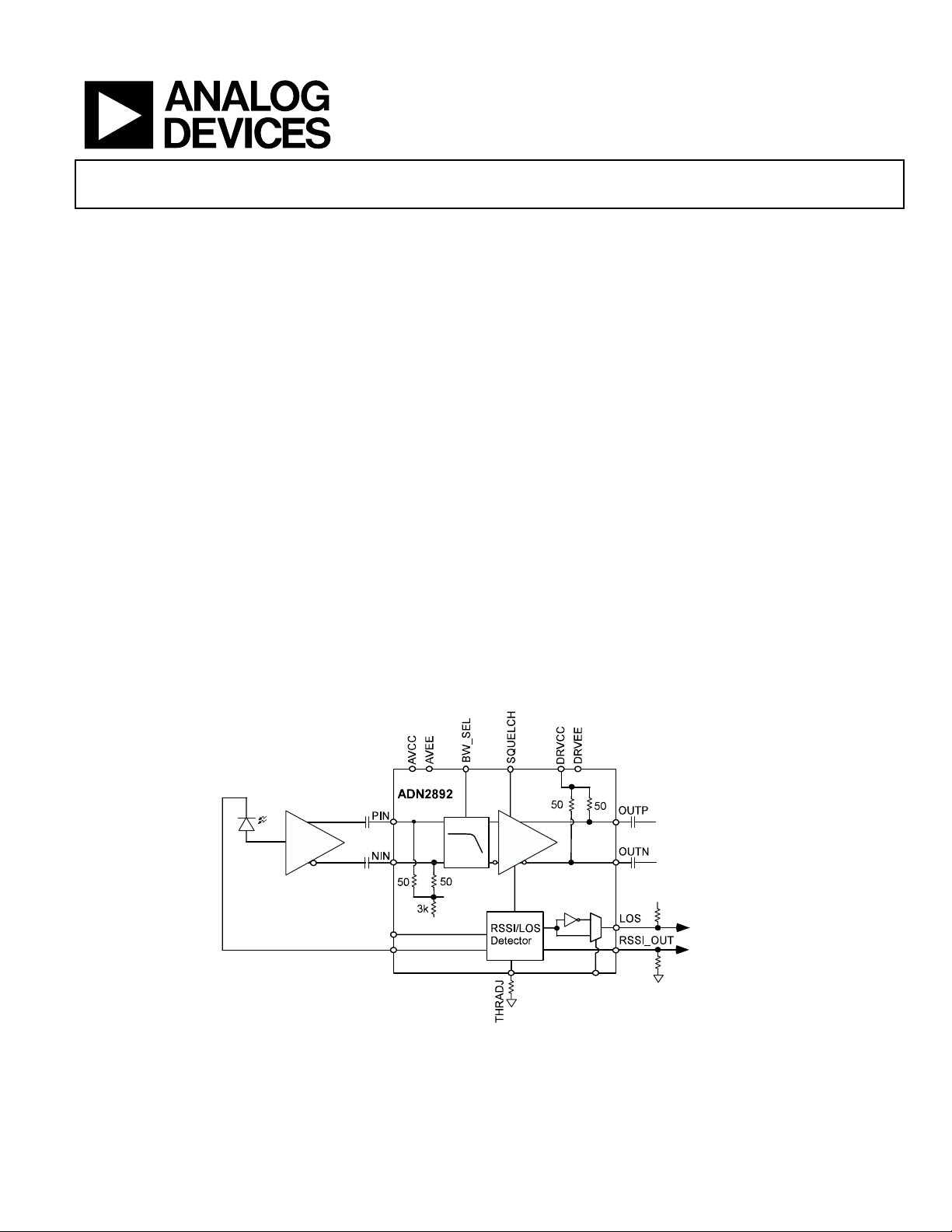
FUNCTIONAL BLOCK DIAGRAM
Limiting Amplifier
ADN2892
The ADN2892 is a high gain, limiting amplifier optimized for
use in Fibre Channel and GbE optical receivers. The ADN2892
accepts input levels of up to 2.0 V p-p differential and has 3 mV
p-p differential input sensitivity. The ADN2892 provides the
receiver functions of quantization and loss of signal (LOS)
detection.
The ADN2892 has an on-chip selectable filter to reduce the BW
of the limamp to 1.5GHz in order to filter out the relaxation
oscillation of legacy 1Gb/s Fiber Channel transmitters with CD
lasers. The reduced BW will also allow for more optical Rx
sensitivity margin at the lower data rates such as 1xFC and
1GbE in multi-rate modules.
The limiting amplifier also measures average received power
based on a direct measurement of the photodiode current with
better than 1 dB of accuracy over the entire input range of the
receiver. This eliminates the need for external average Rx power
detection circuitry in SFF-8472 compliant optical transceivers.
The ADN2892 limiting amplifier operates from a single 3.3 V
supply, has low power dissipation, and is available in a spacesaving 3 × 3 mm 16-lead lead frame chip scale package
(LFCSP).
ADN2882
V
PD_VCC
PD_CATHODE
REF
Rev. PrA.
Information furnished by Analog Devices is believed to be accurate and reliable.
However, no responsibility is assumed by Analog Devices for its use, nor for any
infringements of patents or other rights of third parties that may result from its use.
Specifications subject to change without notice. No license is granted by implication
or otherwise under any patent or patent rights of Analog Devices. Trademarks and
registered trademarks are the property of their respective owners.
Figure 1.
+V
10kΩ
ADuC7020
V
N
I
_
S
O
L
One Technology Way, P.O. Box 9106, Norwood, MA 02062-9106, U.S.A.
Tel: 781.329.4700 www.analog.com
Fax: 781.326.8703 © 2004 Analog Devices, Inc. All rights reserved.
Page 2

ADN2892 Preliminary Technical Data
TABLE OF CONTENTS
Specifications..................................................................................... 3
Loss of Signal (LOS) Detector .....................................................8
Absolute Maximum Ratings............................................................ 5
Thermal Resistance ...................................................................... 5
ESD Caution.................................................................................. 5
Pin Configuration and Function Descriptions............................. 6
Typical Performance Characteristics ............................................. 7
Theory of Operation ........................................................................ 8
LIMAMP ....................................................................................... 8
REVISION HISTORY
Revision A: Initial Version
Received Signal Strength Indicator (RSSI) ................................8
Squelch Mode ................................................................................8
Applications Information.................................................................9
PCB Design Guidelines ................................................................9
Outline Dimensions....................................................................... 11
Ordering Guide .......................................................................... 11
Rev. PrA| Page 2 of 12
Page 3

Preliminary Technical Data ADN2892
SPECIFICATIONS
VCC = V
Table 1.
Parameter Min Typ Max Unit Test Conditions/Comments
QUANTIZER DC CHARACTERISTICS
Input Voltage Range 1.8 2.8 V p-p @ PIN or NIN, dc-coupled
Input Common Mode 2.1 2.7 V DC-coupled
Peak-to-Peak Differential Input Range 2.0 V p-p PIN − NIN, ac-coupled
Input Sensitivity 3 mV p-p
Input Offet Voltage 100 µV
Input RMS Noise 205 µV rms
Input Resistance 50 Ω Single-ended
Input Capacitance 0.65 pF
QUANTIZER AC CHARACTERISTICS
Input Data Rate 1.0
Small Signal Gain 51 dB Differential
S11 -15 dB Differential, f < 4.25 GHz
S22 -15 dB Differential, f < 4.25 GHz
Random Jitter 5 ps rms Input > 10 mV p-p, 4.25Gb/s, PRBS 27 − 1
Deterministic Jitter 10 ps p-p Input > 10 mV p-p, 4.25 Gb/s, PRBS 27 − 1
Low Frequency Cutoff 30 kHz
Power Supply Noise Rejection 45 dB f < 10 MHz
LOSS OF SIGNAL DETECTOR (LOS)
LOS Assert Level TBD 3.0 TBD mV p-p R
TBD 45.0 TBD mV p-p R
LOS Hysteresis 3 TBD dB 4.25Gb/s, PRBS 27 − 1, R
TBD 3 dB 4.25Gb/s, PRBS 27 − 1, R
LOS Assert Time 600 ns DC-coupled
LOS De-Assert Time 100 ns DC-coupled
RSSI
Input Current Range 5 1000 µA
RSSI Output Accuracy 15 %
10 % IIN > 20 µA
Gain 1.0 mA/mA I
Offset 50 nA
Compliance Voltage VCC − 0.9 VCC − 0.3 V @ PD_CATHODE
POWER SUPPLIES
VCC 3.0 3.3 3.6 V
ICC 50 mA
OPERATING TEMPERATURE RANGE −40 +25 +95 °C T
CML OUTPUT CHARACTERISTICS
Output Impedance 50 Ω Single-ended
Output Voltage Swing 600 700 800 V p-p Differential
Output Rise and Fall Time 65 ps 20% to 80%
LOGIC INPUTS
VIH, Input High Voltage 2.0 V
VIL, Input Low Voltage 0.8 V
Input Current −100 nA I
100 nA I
MIN
to V
, VEE = 0 V, TA = T
MAX
MIN
to T
, BW_SEL = 1, unless otherwise noted.
MAX
4.25
1.0
2.125
Gb/s
Gb/s
PIN − NIN, BER ≤ 1 × 10
BW_SEL = 1
BW_SEL = 0
= 100 kΩ
THRADJ
= 0 Ω
THRADJ
I
≤ 20 µA
IN
RSSI/IPD
to T
MAX
MIN
, VIN = 2.4 V
INH
, VIN = 0.4 V
INL
−10
THRADJ
THRADJ
= 0 Ω
= 100 kΩ
Rev. PrA | Page 3 of 12
Page 4

ADN2892 Preliminary Technical Data
Parameter Min Typ Max Unit Test Conditions/Comments
LOGIC OUTPUTS (LOS)
VOH, Output High Voltage 2.4 V
VOL, Output Low Voltage 0.4 V
Open drain output, 4.7 kΩ − 10 kΩ
pull-up resistor to V
Open drain output, 4.7 kΩ − 10 kΩ
pull-up resistor to VCC
CC
Rev. PrA| Page 4 of 12
Page 5

Preliminary Technical Data ADN2892
ABSOLUTE MAXIMUM RATINGS
Table 2.
Parameter Rating
Supply Voltage 4.2 V
Minimum Input Voltage (All Inputs) VEE − 0.4 V
Maximum Input Voltage (All Inputs) VCC + 0.4 V
Storage Temperature −65°C to +155°C
Operating Temperature Range −40°C to +95°C
Lead Temperature Range (Soldering 10 s) 300°C
Junction Temperature 125°C
ESD CAUTION
ESD (electrostatic discharge) sensitive device. Electrostatic charges as high as 4000 V readily accumulate on
the human body and test equipment and can discharge without detection. Although this product features
proprietary ESD protection circuitry, permanent damage may occur on devices subjected to high energy
electrostatic discharges. Therefore, proper ESD precautions are recommended to avoid performance
degradation or loss of functionality.
Stresses above those listed under Absolute Maximum Ratings
may cause permanent damage to the device. This is a stress
rating only and functional operation of the device at these or
any other conditions above those indicated in the operational
section of this specification is not implied. Exposure to absolute
maximum rating conditions for extended periods may affect
device reliability.
THERMAL RESISTANCE
θJA is specified for 4-layer PCB with exposed paddle soldered
to GND.
Table 3.
Package Type
16-lead 3 × 3 mm LFCSP 28 °C/W
θ
JA
Unit
Rev. PrA | Page 5 of 12
Page 6

ADN2892 Preliminary Technical Data
PIN CONFIGURATION AND FUNCTION DESCRIPTIONS
PD_CATHODE
PD_VCC
RSSI_OUT
SQUELCH
161514
13
12
1
AVCC
AVEE
ADN2892A
2
PIN
Top View
3
NIN
4
567
BW_SEL
THRADJ
Figure 2. Pin Configuration
Note: There is an exposed pad on the bottom of the package that must be connected to the GND plane with filled vias.
Table 4. Pin Function Descriptions
Pin No. Mnemonic I/O Description
1 AVCC Power Analog Power
2 PIN Input Differential Data Input
3 NIN Input Differential Data Input
4 AVEE Power Analog Ground
5 THRADJ Input LOS Threshold Adjust Resistor
6 BW_SEL Input Rate Select: BW_SEL = 0 for 1x/2xFC, BW_SEL = 1 for 4xFC
7 LOS_INV Input LOS_INV=1 inverts the LOS output to be active low (for SFF).
8 LOS Output LOS Detector Output
9 DRVEE Power Output Buffer Ground
10 OUTN Output Differential Data Output
11 OUTP Output Differential Data Output
12 DRVCC Power Output Buffer Power
13 SQUELCH Input Disable Outputs
14 RSSI_OUT Output Average Current Output
15 PD_VCC Power Power Input for RSSI Measurement
16 PD_CATHODE Output Photodiode Bias Voltage
Exposed Pad Pad Power Connect to Ground
DRVCC
11
OUTP
10
OUTN
9
DRVEE
8
LOS
LOS_INV
Rev. PrA| Page 6 of 12
Page 7

Preliminary Technical Data ADN2892
TYPICAL PERFORMANCE CHARACTERISTICS
0.96
0.88
0.80
0.72
0.64
0.56
0.48
0.40
RSSI_OUT (mA)
0.32
0.24
0.16
0.08
0
0 0.1 0.2 0.3 0.4 0.5
RSSI_IN (mA)
0.6 0.7 0.8 0.9 1.0
Figure 3. RSSI Output vs. Average PIN Photodiode Current
LOS Trip Point -vs- RTHRADJ
50
40
30
mV
20
10
0
10 100 1000 10000 100000
ohms
Figure 4. LOS Trip Point vs. Threshold Adjust Resistor
70
04509-0-002
Figure 6. S11 Plot—TBD
Figure 7.S22 Plot—TBD
60
50
40
30
20
SUPPLY-NOISE REJECTION (dB)
10
0
100k 1M
SUPPLY-NOISE FREQUENCY (Hz)
10M
04509-0-010
Figure 5. Typical PSRR vs. Supply-Noise Frequency
Rev. PrA | Page 7 of 12
Page 8

ADN2892 Preliminary Technical Data
THEORY OF OPERATION
LIMAMP
Input Buffer
The limiting amplifier has differential inputs (PIN/NIN), with
an internal 50 Ω termination. The ROSA (receive optical subassembly) is typically ac-coupled to the ADN2892 inputs
(although dc coupling is possible).
There is an on-chip, input offset compensation loop with a
30kHz low-frequency cutoff.
CML Output Buffer
The ADN2892 provides CML outputs, OUTP/OUTN. The
outputs are internally terminated with 50 Ω to V
The outputs can be kept at a static voltage by driving the
SQUELCH pin to a logic high. The SQUELCH pin can be
driven directly by the LOS pin, which automatically disables the
LIMAMP outputs in situations with no data input.
.
CC
BANDWIDTH SELECT
The ADN2892 has an on-chip selectable 4th order BesselThomson filter in order to support 1x/2x/4x Fiber Channel
transceivers utilizing rate select. Setting the BW_SEL pin to
logic 0 selects the on-chip filter which reduces the BW of the
limamp to ~1.5GHz. This is sufficient to filter out the relaxation
oscillation from legacy 1Gb/s Fiber Channel transmitters using
CD lasers while still providing enough BW to be backwards
compatible with 1x/2x FC multi-rate SFP modules that don't
use the rate select function.
Setting the BW_SEL pin to a logic 1 sets the bandwidth of the
ADN2892 to the full BW of ~4.25GHz. This rate select protocol
is compliant with SFF-8079 Rev 1.0
LOSS OF SIGNAL (LOS) DETECTOR
The receiver front-end LOS detector circuit indicates when the
input signal level has fallen below a user-adjustable threshold.
The threshold is set by a resistor connected between the
THRADJ pin and V
threshold, the LOS output will assert to a logic 1. There is
hysteresis built into the LOS circuit to prevent chattering at the
LOS output. The LOS hysteresis is typically 5dB.
The LOS output is an open-drain output that needs to be
externally pulled up with a 4.7kΩ-10kΩ resistor. The LOS
output active high by default which is compliant with the SFP
and GBIC MSAs. There is an LOS_INV input which, when set
to a logic 1, inverts the LOS output so that it is active low. This
is in order to support the SFF MSA.
. When the input level drops below this
EE
RECEIVED SIGNAL STRENGTH INDICATOR (RSSI)
The ADN2892 has an on-chip RSSI circuit that automatically
detects the average received power, based on a direct measurement of the PIN photodiode’s current. The photodiode bias is
supplied by the ADN2892, which allows a very accurate, onchip, average power measurement based on the amount of
current supplied to the photodiode. The output of the RSSI is a
current that is directly proportional to the average amount of
PIN photodiode current. Placing a resistor between the
RSSI_OUT pin and GND converts the current to a GND
referenced voltage. This function eliminates the need for
external RSSI circuitry in SFF-8472 compliant optical receivers.
SQUELCH MODE
Driving the SQUELCH input to a logic high disables the
limiting amplifier outputs. The SQUELCH input can be
connected to the LOS output to keep the limiting amplifier
outputs at a static voltage level anytime the input level to the
limiting amplifier drops below the programmed LOS threshold.
Rev. PrA| Page 8 of 12
Page 9

Preliminary Technical Data ADN2892
APPLICATIONS INFORMATION
PCB DESIGN GUIDELINES
Proper RF PCB design techniques must be used for optimal
performance.
Power Supply Connections and Ground Planes
Use of one low impedance ground plane is recommended. The
VEE pins should be soldered directly to the ground plane to
reduce series inductance. If the ground plane is an internal
plane and connections to the ground plane are made through
vias, multiple vias can be used in parallel to reduce the series
inductance, especially on Pin 9, which is the ground return for
the output buffers. The exposed pad should be connected to the
GND plane using filled vias so that solder does not leak through
the vias during reflow. Using filled vias under the package
VCC
C9
E
D
O
T
C
C
V
_
D
P
6
1
connect
exposed
pad to
GND
5
L
E
S
_
W
B
H
U
C
L
O
_
E
I
S
U
S
Q
R
S
4
3
5
1
1
1
12
11
10
9
6
7
8
S
V
O
N
I
L
_
S
O
R3
L
H
T
A
C
_
D
P
1
PIN
2
3
4
J
D
A
R
H
T
R2
Figure 8. Typical ADN2892 Applications Circuit
0.1µF
ADN2882
VCC
VCC
C5 C6
C1
C2
AVC C
NIN
AV EE
C12
DRVCC
OUTP
OUTN
DRVEE
VCC
greatly enhances the reliability of the connectivity of the
exposed pad to the GND plane during reflow.
Use of a 10 µF electrolytic capacitor between VCC and VEE is
recommended at the location where the 3.3 V supply enters the
PCB. When using 0.1 µF and 1 nF ceramic chip capacitors, they
should be placed between the IC power supply VCC and VEE,
as close as possible to the ADN2892 VCC pins.
If connections to the supply and ground are made through vias,
the use of multiple vias in parallel helps to reduce series
inductance, especially on Pin 12, which supplies power to the
high speed OUTP/ OUTN output buffers. Refer to the
schematic in Figure 8 for recommended connections.
RSSI measurement
to ADC
C10R1
VCC
C7 C8
C3
To H os t B o a r d
4.7k - 10k
on host board
C4
C1-C4, C11: 0.01µF X5R/X7R dielectric, 0201 case
C5,C7,C9,C10,C12: 0.1µF X5R/X7R dielectric, 0402 case
C6, C8: 1nF X5R/X7R dielectric, 0201 case
to ADuC7020
Rev. PrA | Page 9 of 12
Page 10

ADN2892 Preliminary Technical Data
PCB Layout
Figure 9 shows a recommended PC board layout. Use of 50 Ω
transmission lines is required for all high frequency input and
output signals to minimize reflections: PIN, NIN, OUTP and
OUTN. It is also necessary for the PIN/NIN input traces to be
matched in length, and OUTP/OUTN output traces to be
matched in length to avoid skew between the differential traces.
C1, C2, C3, and C4 are ac coupling capacitors in series with the
high speed I/O. It is recommended that components be used
such that the pad for the capacitor is the same width as the
transmission line to minimize the mismatch in the 50 Ω
transmission line at the capacitor's pads. It is recommended that
the transmission lines not change layers through vias, if
possible. For supply decoupling, the 1nF decoupling capacitor
should be placed on the same layer as the ADN2892 as close as
possible to the VCC pin. The 0.1uF capacitor can be placed on
the bottom of the PCB directly underneath the 1nF decoupling
capacitor. All high speed CML outputs are back-terminated on
TO ROSA
place C5 on
bottom of board
underneath C6
C6
C1
PIN
NIN
C2
1
~4mm
chip with 50 Ω resistors connected between the output pin and
VCC. The high speed inputs, PIN and NIN, are internally
terminated with 50 Ω to an internal reference voltage.
As with any high speed mixed-signal design, take care to keep
all high speed digital traces away from sensitive analog nodes.
Soldering Guidelines for Chip Scale Package
The lands on the 16 LFCSP are rectangular. The printed circuit
board pad for these should be 0.1 mm longer than the package
land length and 0.05 mm wider than the package land width.
The land should be centered on the pad. This ensures that the
solder joint size is maximized. The bottom of the chip scale
package has a central exposed pad. The pad on the printed
circuit board should be at least as large as this exposed pad. The
user must connect the exposed pad to VEE using filled vias so
that solder does not leak through the vias during reflow. This
ensures a solid connection from the exposed pad to VEE.
R1,C9,C10 on bottom
double-vias to reduce
inductance to supply
and GND
place C7 on
bottom of board
exposed pad
filled
vias to GND
double-via to GND
to reduce inductance
C8
underneath C8
C3
C4
transmission lines same
width as AC coupling
caps to reduce reflections
OUTP
OUTN
Via to C12, R2
on bottom
Vias to bottom
Figure 9. Recommended ADN2892 PCB Layout
Rev. PrA| Page 10 of 12
Page 11

Preliminary Technical Data ADN2892
OUTLINE DIMENSIONS
0.50
0.40
PIN 1
INDICATOR
1.00
0.85
0.80
SEATING
PLANE
12° MAX
3.00
BSC SQ
VIEW
0.30
0.23
0.18
TOP
2.75
BSC SQ
0.80 MAX
0.65 TYP
0.05 MAX
0.02 NOM
0.20 REF
*COMPLIANT TO JEDEC STANDARDS MO-220-VEED-2
EXCEPT FOR EXPOSED PAD DIMENSION
0.45
0.50
BSC
1.50 REF
0.60 MAX
13
12
9
Figure 10. 16-Lead Lead Frame Chip Scale Package [LFCSP]
3 × 3 mm Body
(CP-16-2)
Dimensions shown in millimeters
8
BOTTOM
VIEW
0.30
16
1
4
5
PIN 1
INDICATOR
1.45
1.30 SQ*
1.15
0.25 MIN
ORDERING GUIDE
Model Temperature Range Package Description Package Option
ADN2892ACP-RL –40°C to +95°C 16-LFCSP CP-16-2
ADN2892ACP-RL7 –40°C to +95°C 16-LFCSP CP-16-2
Rev. PrA | Page 11 of 12
Page 12

ADN2892 Preliminary Technical Data
NOTES
© 2004 Analog Devices, Inc. All rights reserved. Trademarks and
registered trademarks are the property of their respective owners.
PR04986-0-6/04(PrA)
Rev. PrA| Page 12 of 12
 Loading...