

Page 1
Ω
3.2 Gbps 3.3 V Low Noise
Preliminary Technical Data
FEATURES
Technology: high performance SiGe
Bandwidth: 2.1GHz minimum
Input noise current density: 8 pA√Hz
Optical sensitivity: −24 dBm
Differential transimpedance: 5000 V/A
Power dissipation: 75 mW
Differential output swing: 250 mV p-p
Input current overload: +3.25 dBm
Output resistance: 50 Ω/side
Low-freq cutoff: 20 kHz
On-chip PD filter: R
RSSI voltage and current ratio: 0.8V/mA
Die size: 0.7 mm × 1.2 mm
APPLICATIONS
3.2 Gbps optical modules
SFF-8472 compliant receivers
PIN/APD-TIA receive optical subassembly
SONET/GbE/FC optical receivers, transceivers, transponders
PRODUCT DESCRIPTION
= 200 Ω CF = 20 pF
F
3.3V
FILTER
IN
VCC_FI L TER
200Ω
20pF
0.85V
GND
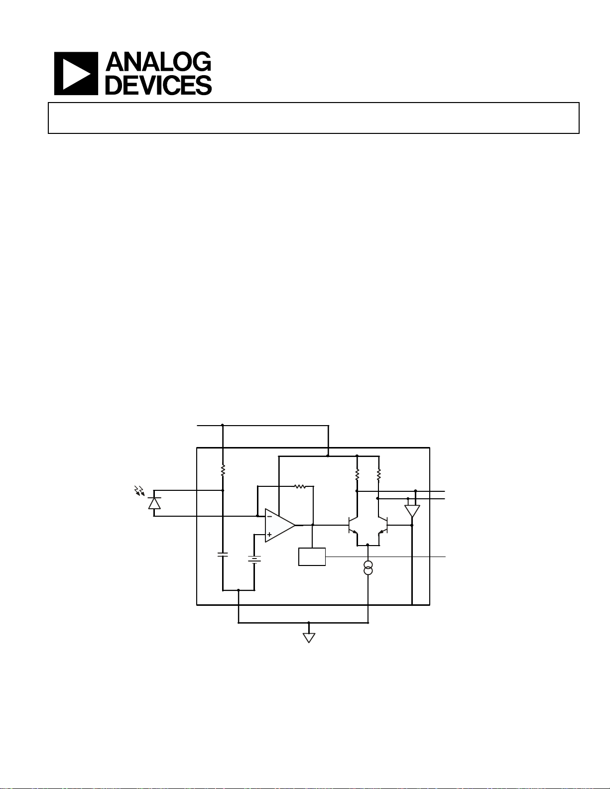
Figure 1. ADN2880 Block Diagram
1400
1100Ω
Transimpedance Amplifier
ADN2880
The ADN2880 is a compact, high performance 3.3 V power
supply SiGe transimpedance amplifier (TIA) optimized for
small-form-factor pluggable (SFP) optical receivers, up to
3.2 Gbps SFF/SPF optical receivers, and meets OC48 SR/IR
sensitivity requirements. The ADN2880 is a single-chip
solution for detecting photodiode current with a differential
output voltage. The ADN2880 features low input referred
noise current of 400 nA enabling −24 dBm sensitivity; 2.1
GHz minimum BW enables up to 3.2 Gbps operation; +3.25
dBm nominal operation at 10 dB extinction ratio. RSSI
output signal proportional to average input current is
available for monitoring and alarm generation. To facilitate
assembly in small form factor packages such as a TO-46 or
TO-56 header, the ADN2880 integrates the photodiode filter
network on chip and features 20 kHz low frequency cutoff
without any external components. The ADN2880 chip area
is less than 1 mm
available in die form.
VCC
GND
2
, operates with a 3.3 V power supply and is
50Ω50Ω
OU T
OU TB
RSSI
5mA
CAP
Rev. PrC
Information furnished by Analog Devices is believed to be accurate and reliable.
However, no responsibility is assumed by Analog Devices for its use, nor for any
infringements of patents or other rights of third parties that may result from its use.
Specifications subject to change without notice. No license is granted by implication
or otherwise under any patent or patent rights of Analog Devices. Trademarks and
registered trademarks are the property of their respective owners.
One Technology Way, P.O. Box 9106, Norwood, MA 02062-9106, U.S.A.
Tel: 781.329.4700 www.analog.com
Fax: 781.326.8703 © 2004 Analog Devices, Inc. All rights reserved.
Page 2

ADN2880 Preliminary Technical Data
TABLE OF CONTENTS
Electrical Specifications ...................................................................3
Pad Layout..........................................................................................6
Absolute Maximum Ratings............................................................ 4
ESD Caution.................................................................................. 4
Pad Descriptions............................................................................... 5
REVISION HISTORY
07/04—Revision PrB
11/04 – Revision C – RSSI added.
Pad Coordinates ............................................................................6
Die Information.............................................................................6
Assembly Recommendations...........................................................7
Rev. PrC | Page 2 of 9
Page 3

Preliminary Technical Data ADN2880
ELECTRICAL SPECIFICATIONS
Table 1.
Parameter Conditions1 Min Typ Max Unit
DYNAMIC PERFORMANCE
Bandwidth (BW)2 −3 dB 2.1 2.3 GHz
Total Input RMS Noise (I
Small Signal Transimpedance (ZT) 100 MHz 4000 5000 6000 V/A
Low Frequency Cutoff CAP = Open
Output Return Loss2 DC to 3.2 GHz, differential −20 −12 dB
Input Overload Current3 Pavg TBD 3.25 dBm
Maximum Output Swing pk-pk diff, I
Output Data Transition Time 20% to 80% rise/fall time I
PSRR < 10 MHz −35 dB
Group Delay Variation 50 MHz to 3.2 GHz TBD ps
Transimpedance Ripple 50 MHz to 3.2 GHz TBD dB
Total Jitter2 10 µA < I
100 µA < I
Deterministic Jitter2 10 µA < I
100 µA < I
DC PERFORMANCE
Power Dissipation I
Input Voltage 0.85 V
Output Common-Mode Voltage DC terminated to Vcc Vcc – 0.12 V
Output Impedance Single-ended 50 Ω
PD FILTER Resistance RF 200 Ω
PD FILTER Capacitance CF 20 pF
)2 DC to 3.2 GHz 375 400 nA
RMS
20 2 kHz
CAP = 1nF
= 2.0 mA 180 250 350 mV
IN,PK- PK
= 2.5 mA 55 ps
IN,PK- PK
≤ 100 µA TBD TBD ps
IN,PK- PK
≤ 2.0 µA TBD TBD ps
IN,PK- PK
≤ 100 µA 4 ps
IN,PK- PK
≤ 2.0 µA 8 ps
IN,PK- PK
= 0 mA 50 75 120 mW
IN,AVE
kHz
RSSI Sensitivity I
RSSI Offset I
= 0 uA to 1 mA 0.8 V/mA
IN, AVE
= 0 uA TBD mV
IN, AVE
1
Min/Max Vcc = +3.3V ± 0.3V, T
2
Photodiode capacitance CD = 0.7 pF ± 0.15 pF, photodiode resistance = 5 Ω input wire bond inductance LIN = 0.3nH ± 0.1nH, Output bond wire inductance L
0.8nH ± 0.1nH Load impedance = 50 Ω (each output, ac-coupled)
3
-10
10
BER, 10dB ER, 0.85 A/W PIN responsivity
= −40 °C to +95°C; Typ Vcc=3.3V, T
ambient
ambient
= +25C
OUT,OUTB
=
Rev. PrC | Page 3 of 9
Page 4

ADN2880 Preliminary Technical Data
ABSOLUTE MAXIMUM RATINGS
Table 2.
Parameters Ratings
Supply Voltage (Vcc to GND) 5 V
Internal Power Dissipation
Output Short Circuit Duration TBD
Maximum Input Current 10 mA
Storage Temperature Range −65°C to +125°C
Operating Ambient Temperature Range −40°C to +95°C
Maximum Junction Temperature 165°C
Die Attach Temperature (<60 seconds) 450°C
ESD CAUTION
ESD (electrostatic discharge) sensitive device. Electrostatic charges as high as 4000 V readily accumulate on the
human body and test equipment and can discharge without detection. Although this product features
proprietary ESD protection circuitry, permanent damage may occur on devices subjected to high energy
electrostatic discharges. Therefore, proper ESD precautions are recommended to avoid performance
degradation or loss of functionality.
Stresses above those listed under ‘Absolute Maximum Rating’
may cause permanent damage to the device. This is a stress
rating only and functional operation of the device at these or
any other conditions above those indicated in the operational
section of this specification is not implied. Exposure to absolute
maximum rating conditions for extended periods may affect
device reliability.
Rev. PrC | Page 4 of 9
Page 5

Preliminary Technical Data ADN2880
PAD DESCRIPTIONS
FILTER
Table 3.
PAD # PAD FUNCTION
1 GND Ground (input return).
2 IN Current Input. Bond directly to PD anode.
3 TEST Test Probe Pad. Leave Floating.
4 FILTER Filter Output.
5 FILTER Filter Output
6 GND Ground.
7 RSSI Voltage Output (provides average input current reading)
8 CAP Low Frequency Setpoint. Connect with 1 nF capacitance to GND for < 30 kHz.
9 GND Ground.
10 GND Ground (output return).
11 OUTB Negative Output. Drives 50 ohm termination (ac or dc termination).
12 OUT Positive Output. Drives 50 ohm termination (ac or dc termination).
13 GND Ground (output return).
14 GND Ground
15 VCCFILTER Filter Supply. Connect to Vcc to enable on-chip 200 Ω*20 pf filter.
16 VCC 3.3 V Positive Supply. Recommended bypass to GND is 100 pF RF capacitor.
17 VCC 3.3 V Positive Supply. Recommended bypass to GND is 100 pF RF capacitor.
B
Rev. PrC | Page 5 of 9
Page 6

ADN2880 Preliminary Technical Data
PAD LAYOUT
FILTER
Figure 2.. Pad Layout
B
PAD COORDINATES
Table 4.
PAD # PAD X (um) Y (um)
1 GND −500 260
2 IN −500 130
3 TEST −500 10
4 FILTER −500 −120
5 FILTER −500 −260
6 GND −350 −260
7 RSSI −200 −260
8 CAP −50 −260
9 GND 130 −260
10 GND 500 −260
11 OUTB 350 −60
12 OUT 350 60
13 GND 500 260
14 GND 130 260
15 VCCFILTER −50 260
16 VCC −200 260
17 VCC −350 260
DIE INFORMATION
Die Size
0.7mm × 1.2mm
(edge-edge including 1mil scribe)
Die Thickness
10mils = 0.25mm
Passivation Openings
0.075 mm × 0.075 mm
(pads 1-8, 9, 10, 13, 15, 16, 17)
0.144mm × 0.075mm
(pads 9, 11, 12, 14)
Passivation Composition
5000Å Si3N4 (top)
+5000 Å SiO
Pad Composition
Al/1%Cu
Backside Contact
(bot)
2
Rev. PrC | Page 6 of 9
Page 7

Preliminary Technical Data ADN2880
ASSEMBLY RECOMMENDATIONS
VPD
560pF
1000pF
OUTB
Figure 3. 5-Pin TO-46 with External Photodiode Supply V
VCC
200pF
OUT
Connected through FILTER Pin
PD
1× Vendor Specific (0.3 mm × 0.3 mm) 2.5 Gbps Photo Diode
1× ADN2880 (0.7mm × 1.2 mm) Analog Devices SiGe 3.2 Gbps Transimpedance Amplifier
1× 200 pF RF Single-Layer Capacitor
1× 560 pF RF Single Layer Capacitor
1x 1000pF Ceramic Capacitor
Notes
Minimize all GND bond wire lengths
Minimize IN, OUT and OUTB bond wire lengths
Maintain symmetry in length and orientation between OUT and OUTB bond wires
Maintain symmetry between IN and OUT/OUTB bond wires
Rev. PrC | Page 7 of 9
Page 8

ADN2880 Preliminary Technical Data
VCC
200pF
OUTB
Figure 4. Recommended Layout of 4-Pin TO-46
Ceramic
Standoff
OUT
1× Vendor Specific (0.3 mm × 0.3 mm) 2.5 Gbps Photo Diode
1× ADN2880 (0.7mm × 1.2 mm) Analog Devices SiGe 3.2 Gbps Transimpedance Amplifier
1× 200 pF RF Single-Layer Capacitor
1× Ceramic Standoff
1x 1000pF Ceramic Capacitor
Notes
Minimize all GND bond wire lengths
Minimize IN, OUT and OUTB bond wire lengths
Maintain symmetry in length and orientation between OUT and OUTB bond wires
Maintain symmetry between IN and OUT/OUTB bond wires
Rev. PrC | Page 8 of 9
Page 9

Preliminary Technical Data ADN2880
ORDERING GUIDE
Model Temperature Package Description Package Option
ADN2880XCHIPS-WP -40oC to 95oC NA Tested Die
© 2004 Analog Devices, Inc. All rights reserved. Trademarks and
registered trademarks are the property of their respective companies.
PR04945–0–11/04(PrC)
Rev. PrC | Page 9 of 9
 Loading...