

Datasheet ADN2850ACP25-RL7, ADN2850ARU25-REEL7, ADN2850ARU25, ADN2850ACP250-RL7, ADN2850ACP250 Datasheet (Analog Devices)
Page 1

PRELIMINARY TECHNICAL DATA
Nonvolatile Memory, Dual 1024
a
Position Programmable Resistors
Preliminary Technical Data ADN2850
FEATURES
Dual, 1024 Position Resolution
25K, 250K Ohm Full Scale Resistance
Low Temperature Coefficient -- 35ppm/°C
Nonvolatile Memory
1
Preset Maintains Wiper Settings
Wiper Settings Read Back
Linear Increment/Decrement
Log taper Increment/Decrement
SPI Compatible Serial Interface
+3V to +5V Single Supply or ±2.5V Dual Supply
26 bytes User Nonvolatile Memory for Constant Storage with
Current Monitoring Configurable Function
APPLICATIONS
SONET, SDH, ATM, Gigabit Ethernet, DWDM Laser Diode
Driver Optical Supervisory Systems
GENERAL DESCRIPTION
The ADN2850 provides dual channel, digitally controlled
programmable resistors
devices perform the same electronic adjustment function as a
mechanical rheostat. The ADN2850’s versatile programming via a
standard serial interface allows sixteen mode of operations and
adjustment including scratch pad programming, memory storing
and retrieving, increment/decrement, log taper adjustment, wiper
setting readback, and extra user defined EEMEM.
In the scratch pad programming mode, a specific setting can be
programmed directly to the RDAC
resistance between terminals W-and-B. The RDAC register can
also be loaded with a value previously stored in the EEMEM
register. The value in the EEMEM can be changed or protected.
When changes are made to the RDAC register, t he value of the new
setting can be saved into the EEMEM. Thereafter, such value will
be transferred automatically to the RDAC register during system
power ON. It is enabled by the internal preset strobe. EEME M can
also be retrieved through direct programming and external preset
pin control.
Other key mode of operations include linear step increment and
decrement commands such that the setting in the RDAC register
can be moved UP or DOWN, on e st ep at a time. For logarithmic
changes in wiper setting, a left/right bit shift command adjusts the
level in ±6dB steps.
The ADN2850 is available in the 5mm x 5mm LFCSP-16 Lead
Frame Chip Scale and thin TSSOP-16 packages. All p arts are
guaranteed to operate over the extended industrial temperature
range of -40°C to +85°C.
2
with resolution of 1024 positions. These
2
register, which sets the
1
FUNCTIONAL BLOCK DIAGRAM
CS
CLK
SDI
SDO
RDY
V
V
GND
PR
WP
DD
SS
ADDRESS
DECODE
SERIAL
INPUT
REGISTER
PWR ON
PRESET
EEMEM
CONTROL
26 BYTES
USER EEMEM
100%
75%
50%
25%
RW B(D) [% of Full Scale RW B]
0%
0 256 512 768
Figure 1. RWB(D) vs Decimal Code
Notes:
1. The term nonvo latile memory and EEMEM a re used interchangebly
2. The term programmable resistor and RDAC are used interchangebly
RDAC1
REGISTER
EEMEM1
RDAC2
REGISTER
EEMEM2
D - C o d e in De c im al
RDAC1
RDAC1
CURRENT
MONITOR
I
1
I
2
1023
W1
W2
B1
B2
V
1
V
2
REV PrH, 13, AUG 2001
Information furnished by Analog Devices is believ ed to be accurate and reli able. However, no
responsibility is assumed by Analog Devices for its use; nor for any infringements of patents or
other rights of third parties which may result fr om its us e. No lic ense is granted by im plic ation
or otherwise under any patent or patent rights of Analog Devices.
One Technology Way, P.O. Box 9106,
Tel: 617/329-4700 Fax:617/326-8703
Norwood, MA 02062-9106 U.S.A.
Page 2

PRELIMINARY TECHNICAL DATA
Nonvolatile Memory Programmable Resistors
ELECTRICAL CHARACTERISTICS 25K , 250K OHM VERSIONS
-40°C < T
Parameter Symbol Conditions Min Typ
< +85°C unless otherwise noted12.)
A
(VDD = +3V to +5.5V and,
ADN2850
1
Max Units
DC CHARACTERISTICS RHEOSTAT MODE Specifications apply to all VRs
Resistor Differential Nonlinearity
Resistor Integral Nonlinearity
2
2
R-DNL R
R-INL R
WB
WB
-2 +2 LSB
-4 +4 LSB
Resistance Temperature Coefficent ∆RWB/∆T 35 ppm/°C
Wiper Resistance R
W
Channel Resistance Matching ∆RWB/R
Nominal Resistor t olerance ∆R
WB
VDD = +5V, IW = 1V/R
VDD = +3V, IW = 1V/R
Ch 1 and 2 RWB, Dx = 3FF
WB
Dx = 3FF
WB
WB
H
H
-30 30 %
50 100 Ω
200 Ω
0.2 %
RESISTOR TERMINALS
Terminal Voltage Range
Capacitance4 Bx C
Capacitance4 Wx C
Common-mode Leakage Current
3
5
V
W, B
B
W
I
CM
f = 1 MHz, measured to GND, Code = Half-scale 8 pF
f = 1 MHz, measured to GND, Code = Half-scale 80 pF
VW = VB = VDD/2 0.01 1 µA
V
SS
V
DD
DIGITAL INPUTS & OUTPUTS
Input Logic High V
Input Logic Low V
Input Logic High V
Input Logic Low V
Input Logic High V
Input Logic Low V
Output Logic High (SDO, RDY) V
Output Logic Low V
Input Current I
Input Capacitance
4
IH
IL
IH
IL
IH
IL
OH
OL
IL
C
IL
with respect to GND, VDD = 5V 2.4 V
with respect to GND, VDD = 5V 0.8 V
with respect to GND, VDD = 3V 2.1 V
with respect to GND, VDD = 3V 0.6 V
with respect to GND, VDD = +2.5V, VSS=-2.5V 2.0 V
with respect to GND, VDD = 5V, VSS=-2.5V 0.5 V
R
= 2.2KΩ to +5V 4.9 V
PULL-UP
IOL = 1.6mA, V
VIN = 0V or V
= +5V 0.4 V
LOGIC
DD
±1 µA
5pF
POWER SUPPLIES
Single-Supply Power Range V
DD
Dual-Supply Power Range VDD/V
Positive Supply Current I
Programming Mode Current I
Read Mode Current I
Negative Supply Current I
Power Dissipation
6
DD
DD(PG)
DD(READ)
SS
P
DISS
VSS = 0V 3.0 5.5 V
SS
±2.25 ±2.75 V
VIH = VDD or VIL = GND 2 20 µA
VIH = VDD or VIL = GND 35 mA
VIH = VDD or VIL = GND 3 mA
VIH = VDD or VIL = GND, V
= 2.5V, V
DD
= -2.5V 2 20 µA
SS
VIH = VDD or VIL = GND 6 110 µW
Power Supply Sensitivity PSS ∆VDD = +5V ±10% 0.002 0.01 %/%
CURRENT MONITOR Terminals
Current Sink at V
Current Sink at V
DYNAMIC CHARACTERISTICS
Resistor Noise Spectral Density e
7
1
2
4, 8
I
1
I
2
N_WB
0.0001 10 mA
10 mA
R
= 25KΩ / 250KΩ, TA = 25oC 20 / 64 nV√Hz
WB_FS
Analog Crosstalk (CW1/CW2)CTVB1 = VB2 = 0V, Measured VW1 with
V
= 100 mV p-p @ f = 100 kHz, Code
W2
1,2
= 200
H
-65 dB
NOTES: See bottom of table next page.
V
REV PrH, 13, AUG 2001 2
Page 3

PRELIMINARY TECHNICAL DATA
Nonvolatile Memory Programmable Resistors
ELECTRICAL CHARACTERISTICS 25K , 250K OHM VERSIONS
-40°C < T
Parameter Symbol Conditions Min Typ
< +85°C unless otherwise noted12.)
A
(VDD = +3V to +5.5V and,
ADN2850
1
Max Units
INTERFACE TIMING CHARACTERISTICS applies to all parts(Notes 4, 9)
Clock Cycle Time (t
CS Setup Time t
CLK Shutdown Time to CS rise t
)t
CYC
1
2
3
20 ns
10 ns
1t
CYC
Input Clock Pulse Width t 4 , t 5Clock level high or low 10 ns
Data Setup Time t
Data Hold Time t
CS to SDO - SPI line acquire t
CS to SDO - SPI line release t
CLK to SDO Propagation Delay
10
CLK to SDO Data Hold Time t
CS High Pulse Width t
CS High to CS High t
RDY Rise to CS Fall t
CS Rise to RDY fall time t
Read/Store to Nonvolatile EEMEM
11
CS Rise to Clock Edge Setup t
Preset Pulse Width (Asynchronous) t
Preset Response Time to RDY High t
FLASH/EE MEMORY RELIABILITY
13
6
7
8
9
t
10
11
12
13
14
15
t
16
17
PRW
PRESP
From Positive CLK transition 5 ns
From Positive CLK transition 5 ns
640 ns
34 100 ns
RP = 2.2KΩ, CL < 20pF 34 100 ns
RP = 2.2KΩ, CL < 20pF 0 ns
10 ns
4t
CYC
01 µs
0.11 ms
Applies to Command 2H, 3H, 9
H
25 ms
10 ns
Not shown in timing diagram 50 ns
PR pulsed low to refreshed wiper positions 70 us
Endurance 100,000 Cycles
Data Retention
14
100 Years
NOTES:
1. Typicals represent average readings at +25°C and VDD = +5V.
2. Resistor position nonlinearity error R-INL is the deviation from an ideal value measured between the maximum resistance and the minimum resistance wiper positions. R-DNL measures the
relative step change from ideal between successive tap positions. I
3. Resistor terminals W,B have no limitations on polarity with respect to each other.
4. Guaranteed by design and not subject to production test.
5. Common mode leakage current is a measure of the DC leakage from any terminal B and W to a common mode bias level of V
6. P
7. Applies to Photo Diode of Optical Receiver.
8. All dynamic characteristics use V
9. See timing diagram for location of measured values. All input control voltages are specified with t
10. Propagation delay depends on value of V
11. RDY pin low only for commands 2, 3, 8, 9, 10, and PR hardware pulse: CMD_8 ~ 1ms; CMD_9,10 ~0.1ms; CMD_2,3 ~20ms. Device operation at T
12. Parts can be operated at +2.7V single supply, except from 0
13. The ADN2850 contains 16,000 transistors. Die size: 100 mil x 150 mil, 10,500 sq. mil.
14. Retention lifetime equivalent at junction temperature (T
Specifications Subject to Change without Notice
is calculated from (IDD x VDD) + (ISS x VSS)
DISS
= +5V and V
DD
are measured using both V
to 35ms.
temperature as shown in Figure xxx in the Flash/EE Memory description sect ion of this data sheet.
= +3V and +5V.
DD
= 0V
SS
, R
, and CL see applications text.
DD
PULL_UP
) = 55°C as per JEDEC Std. 22, Method A117. Retention lifetime based on an activation energy of 0.6eV will derate with junction
J
~ 50uA for VDD= +2.7V and IW ~ 400uA for VDD=+5V. See test circuit f igure xxxx
W
/ 2.
DD
=2.5ns(10% to 90% of 3V) and timed from a voltage level of 1.5V. Switching characteristics
R=tF
o
C to –40oC where minimum +3V is needed
=-40oC & VDD<+3V extends the save time
A
REV PrH, 13, AUG 2001 3
Page 4
PRELIMINARY TECHNICAL DATA
Nonvolatile Memory Programmable Resistors
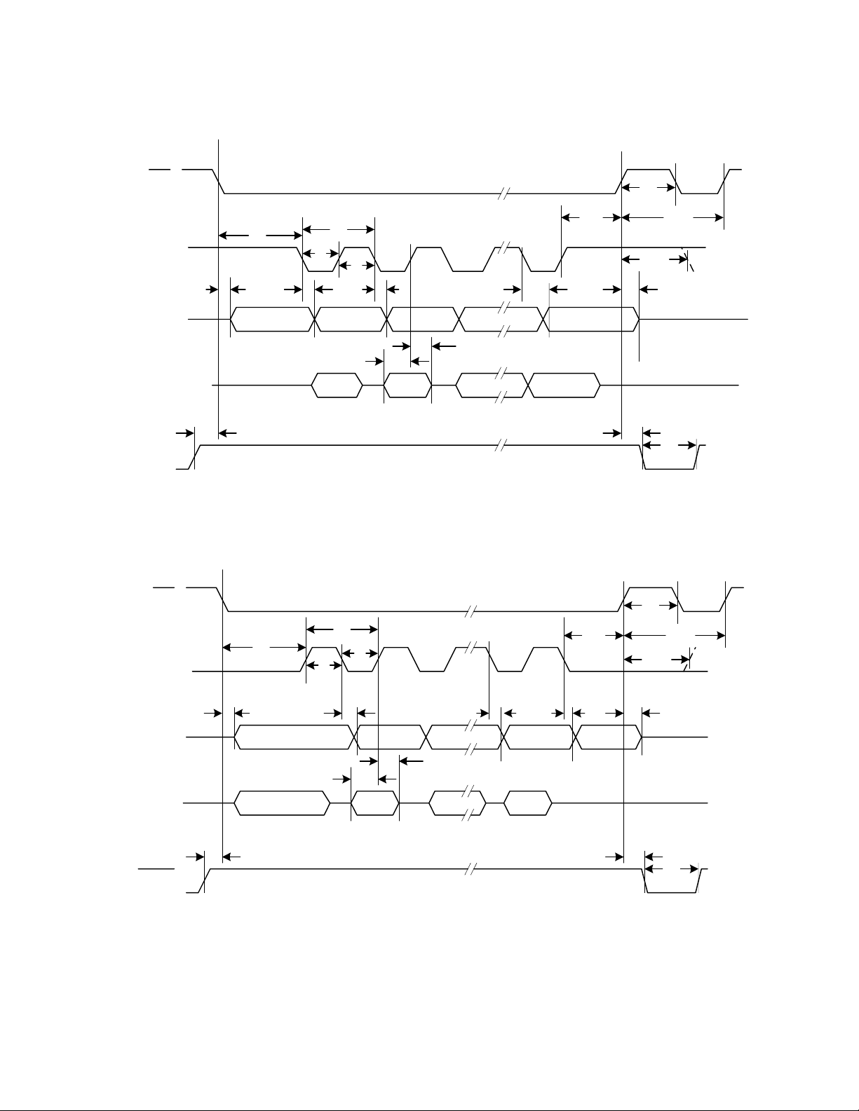
Timing Diagram
CPHA = 1
CS
t
t
1
t
5
t
4
t
10
MSB LSB OUT
t
7
t
6
MSB LSB
CLK
CPOL=1
SDO
SDI
t
2
t
t
8
10
*
t
14
RDY
Note: Not d efined, but normally LS B of character prev iously transmitted
*
* Note: Not defined, but normally LSB of character previously transmitted. The CPOL=1 micro
To be fully compliant the CPHA=1, CPOL=1 mode should be used when shifting more
controller command aligns the incoming data to the positive edge of the clock.
than 8-bits to gether as the
of a serial command will not take place until
controller command aligns the incoming data to the positive edge of the clock .
line can remain low (useful for daisy chaining). Processing
CS
returns high. The CPOL = 0 micro
CS
Figure 2A. CPHA=1 Timing Diagram
CPHA = 0
CS
t
1
t
5
t
4
CLK
CPOL=0
t
2
t
11
3
t
9
t
15
t
3
ADN2850
t
12
t
13
t
17
t
16
t
12
t
13
t
17
SDO
SDI
t
8
MSB OUT LSB
MSB IN LSB
t
14
t
10
t
7
t
6
RDY
Note: Not defined, but normally MSB of character just received
*
* Note: Not defined, but normally MSB of character just received. The CPOL=0 micro controller
can remain low for the CPHA=0, CPOL=0 mode between multiple bytes;
CS
command aligns the incoming data to the positive edge of the clock.
however this is not strictly SPI compliant. The CPOL = 0 micro controller
command aligns t he incoming data to the pos itive edge of the clock .
Figure 2B. CPHA=0 Timing Diagram
REV PrH, 13, AUG 2001 4
t
11
t
11
t
9
*
t
15
t
16
Page 5

PRELIMINARY TECHNICAL DATA
Nonvolatile Memory Programmable Resistors
Absolute Maximum Rating1 (
TA = +25°C, unless
otherwise noted)
to GND............................................................-0.3V, +7V
V
DD
to GND ............................................................+0.3V, -7V
V
SS
to VSS.........................................................................+7V
V
DD
V
, VW to GND..................................... VSS-0.3V, VDD+0.3V
B
– WX.......................................................................±20mA
B
X
Intermittent2..................................................±20mA
Continuous...................................................±1.3mA
Digital Inputs & Output Voltage to GND.....-0.3V, V
Operating Temperature Range
Maximum Junction Temperature (T
Storage Temperature......................................-65°C to +150°C
Lead Temperature, Soldering
3
........................-40°C to +85°C
)...................+150°C
MAX
J
4
DD
+0.3V
Vapor Phase (60 sec).......................................+215 °C
Infrared (15 sec)...............................................+220 °C
Thermal Resistance Junction-to-Ambient
θ
JA,
LFCSP-16........................................................35°C/W
TSSOP-16 ..................................................... 150°C/W
Thermal Resistance Junction-to-Case
LFCSP-16............................................................. TBD
TSSOP-16 ....................................................... 28°C/W
Package Power Dissipation = (TJMAX - TA) / θ
NOTES
1. Stresses above those listed under Absolute Maximum Ratings may
cause permanent damage to the device. This is a stress rating; functional
operation of t he device at these or any other conditions above those
listed in the operational sections of this specification is not implied.
Exposure to absolute maximum rating conditions for extended periods
may affect device reliability.
2. Maximum terminal current is bounded by the maximum current
handling of the switches, maximum power dissipation of the package,
and maximum applied voltage across any two of the B, and W termi nals
at a given resistance.
3. Includes programming of Nonvolatile memory
4. Applicable to TSSOP-16 only. For LFCSP-16, please consult factory
for detail
ADN2850
θ
JC,
JA
Ordering Guide
Model R
ADN2850ACP25 25 ±2 ±4 -40/+85°C LFCSP-16 CP-16 ACP25
ADN2850ACP25-RL7 25 ±2 ±4 -40/+85°C LFCSP-16
ADN2850ACP250 250 ±2 ±4 -40/+85°C LFCSP-16 CP-16 ACP250
ADN2850ACP250-RL7 250 ±2 ±4 -40/+85°C LFCSP-16
ADN2850ARU25 25 ±2 ±4 -40/+85°C TSSOP-16 RU-16 ARU25
ADN2850ARU25-REEL7 25 ±2 ±4 -40/+85°C TSSOP-16
* Line 1 contains ADI logo symbol and date code YYWW, line 2 contains product number ADN2850, line 3 branding containing differentiating detail by part type, line
4 contains lot number.
WB
(k Ohm)
RDNL
(LSB)
RINL
(LSB)
Temp
Range
Package
Description
1500 Pieces
7” Reel
1500 Pieces
7” Reel
1000 Pieces
7” Reel
Package
Option
CP-16 ACP25
CP-16 ACP250
RU-16 ARU25
Top Mark*
CAUTION
ESD (electrostatic discharge) sensitive device. Electrostatic charges as high as 4000 V readily
accumulate on the human body and test equipment and can discharge without detection. Although the
ADN2850 features proprietary ESD protection circuitry, permanent damage may occur on devices
subjected to high-energy electrostatic discharges. Therefore, p r oper ESD precaution s are recommended
to avoid performance degradation or loss of functionality.
REV PrH, 13, AUG 2001 5
Page 6

PRELIMINARY TECHNICAL DATA
Nonvolatile Memory Programmable Resistors
ADN2850ACP PIN CONFIGURATION
CS
PR
12
WP
11
V
DD
10
V
2
9
SDO
GND
V
V
SS
1
SDI CLK RDY
16 15 14 13
1
2
3
4
5678
W1 B1 B2 W2
ADN2850ACP PIN DESCRIPTION
#Name Description
1 SDO Serial Data Output Pin. Open Drain Output requires
2 GND Ground pin, logic ground reference
3V
4V
SS
1
5 W1 Wiper terminal of RDAC1 . ADDR(RDAC1) = 0
6 B1 B terminal of RDAC1
7 B2 B terminal of RDAC2.
8 W2 Wiper terminal of RDAC2 . ADDR(RDAC2) = 1
9V
10 V
2
DD
11 WP Write Protect Pin. When active low, WP prevents
12 PR Hardware over ride preset pin. Refreshes the scratch
13 CS Serial Register chip select active low. Serial register
14 RDY Ready. Active-high open drain output. Identifies
15 CLK Serial Input Register clock pin. Shifts in one bit at a
16 SDI Serial Data Input Pin. Shifts in one bit at a time on
external pull-up resistor. Commands 9 and 10
activate the SDO output. See Instr uction operation
Truth Table. Table 2. Other commands shift out the
previously loaded SDI bit pattern delayed by 24
clock pulses. This allows daisy-chain operation of
multiple packages.
Negative Supply. Connect to zero volts for single
supply applications.
Log Output Voltage 1 generated from internal diode
configured transistor
H
H
Log Output Voltage 2 generated from internal diode
configured transistor
Positive Power Supply Pin.
any changes to the pres ent register contents, except
PR and cmd 1 and 8 will refresh the RDAC register
from EEMEM.
pad register with current contents of the EEMEM
register. Factory default loads midscale 512
10
until
EEMEM loaded with a new value by the user (PR is
activated at the logic high transition).
operation takes place when CS returns to logic h igh.
completion of commands 2, 3, 8, 9, 10, and PR.
time on positive clock edges.
positive clock CLK edges. MSB loaded firs t.
ADN2850ARU PIN DESCRIPTION
#Name Description
1 CLK Serial Input Register clock pin. Shifts in one bit at a
2 SDI Serial Data Input Pin. Shifts in one bit at a time on
3 SDO Serial Data Output Pin. Open Drain Output requires
4 GND Ground pin, logic ground reference
.
.
5V
6V
7 W1 Wiper terminal of RDAC1. ADDR(RDAC1) = 0
8 B1 B terminal of RDAC1
9 B2 B terminal of RDAC2.
10 W2 Wiper terminal of RDAC2. ADDR(RDAC2) = 1
11 V
12 V
13 WP Write Protect Pin. When active low, WP prevents
14 PR Hardware over ride preset pin. Refreshes the sc ratch
15 CS Serial Register chip select active low. Serial register
16 RDY Ready. Active-high open drain output. Identifies
ADN2850ARU PIN CONFIGURATION
1
CLK
2
SDI
SDO
3
4
GND
V
5
SS
V
6
1
7
W1
B1
8
time on positive clock edges.
positive clock CLK edges. MSB loaded first.
external pull-up resistor. Commands 9 and 10
activate the SDO output. See Instr uction operation
Truth Table. Table 2. Other commands shift out the
previously loaded SDI bit pattern delayed by 24
clock pulses. This allows daisy-chain operation of
multiple packages
SS
1
2
DD
Negative Supply. Connect to zero volts for single
supply applications.
Log Output Voltage 1 generated from internal diode
configured transistor
Log Output Voltage 2 generated from internal diode
configured transistor
Positive Power Supply Pin.
any chan ges to the pres ent contents except PR and
cmd 1 and 8 will refresh the RDAC register from
E2MEM.
pad register with current contents of the EEMEM
register. Factory default loads midscale 512
EEMEM loaded with a new value by the user (PR is
activated at the logic high transition).
operation takes place when CS returns to logic h igh.
completion of commands 2, 3, 8, 9, 10, and PR.
ADN2850
16
RDY
CS
CS
CSCS
15
PR
PR
PRPR
14
WP
WP
WPWP
13
V
12
DD
V
11
2
W2
10
B2
9
until
10
.
H
.
H
REV PrH, 13, AUG 2001 6
Page 7

PRELIMINARY TECHNICAL DATA
Nonvolatile Memory Programmable Resistors
ADN2850
Table 1. ADN2850 24-bit Serial Data Word
MSB LSB
RDAC
EEMEM
Command bits are C0 to C3. Address bits are A3-A0. Data bits D0 to D9 are applicable to RDAC whereas D0 to D15 are applicable to EEMEM. Command
instruction codes are defined in table 2.
Table 2. ADN2850 Instruction/Operation Truth Table
Inst
No.
0 0 0 0 0 X X X X X ••• X X X ••• X
1 0 0 0 1 0 0 0 A0 X ••• X X X ••• X
2 0 0 1 0 0 0 0 A0 X ••• X X X ••• X
3
4
5
6
7
8 1 0 0 0 0 0 0 0 X ••• X X X ••• X
9 1 0 0 1 << ADDR >> X ••• X X X ••• X
10 1 0 1 0 0 0 0 A0 X ••• X X X ••• X
11 1 0 1 1 0 0 0 A0 X ••• D9 D8 D7 ••• D0
12c1 1 0 0 0 0 0 A0 X ••• X X X ••• X
13c1 1 0 1 X X X X X ••• X X X ••• X
14c1 1 1 0 0 0 0 A0 X ••• X X X ••• X
15c1 1 1 1 X X X X X ••• X X X ••• X
NOTES:
a) The SDO output shifts-out the last 24-bits of data clocked into the serial register for daisy chain operation. Exception, following Instruction #9 or #10
b) The RDAC register is a volatile scratch pad register that is refreshed at power ON from the corresponding non-volatile EEMEM register.
c) The increment, decrement and shift commands ignore the contents of the shift register Data Bytes 0 and 1.
d) Execution of the above Operations takes place when the CS strob e returns to logic high.
e) Instruction #3 write two data bytes to EEMEM. But in the cases of addresses 0 and 1, only the last 10 bits are valid for wiper position setting.
REV PrH, 13, AUG 2001 7
C3C2C1C0000A0XXXXXXD9D8D7D6D5D4D3D2D1D0
C3 C2 C1 C0 A3 A2 A1 A0 D15D14D13D12D11D10D9 D8 D7 D6 D5 D4 D3 D2 D1 D0
a,b,d
Instruction Byte 0
B23 ••••••••••••••• B16
C3 C2 C1 C0 A3 A2 A1 A0 X ••• D9 D8 D7 ••• D0
e
0 0 1 1 << ADDR >> D15 ••• D8 D7 ••• D0
c
0 1 0 0 0 0 0 A0 X ••• X X X ••• X
c
0 1 0 1 X X X X X ••• X X X ••• X
c
0 1 1 0 0 0 0 A0 X ••• X X X ••• X
c
0 1 1 1 X X X X X ••• X X X ••• X
the selected internal register data will be present in data byte 0 & 1. Instructions following #9 & #10 must be a full 24-bit data word to completely
clock out the contents of the serial register.
Data Byte 1
B15 •••• B8
Data Byte 0
B7 ••• B0
Operation
NOP: Do nothing
Write contents of EEMEM(A0) to RDAC(A0)
Register). This command leaves device in the Read
Program power state. To return part to the idle
state, perform NOP instruction #0
SAVE WIPER SETTING: Write contents of
RDAC(A0) to EEMEM(A0)
Write contents of Serial Register Data Bytes 0 & 1
to EEMEM(ADDR)
Decrement 6dB: Right Shift contents of RDAC(A0),
steops at all “Zeros”.
Decrement All 6dB: Right Shift contents of all
RDAC Registers, stops at all “Zeros”.
Decrement contents of RDAC(A0) by “One”, stops
at all “Zero”.
Decrement contents of all RDAC Register by “One”,
stops at all “Zero”.
RESET: Load all RDACs with their corresponding
EEMEM previously-saved values
Write contents of EEMEM(ADDR) to Serial Register
Data Bytes 0 & 1. SDO activated. See Figure xxxx
Write contents of RDAC(A0) to Serial Register Data
Bytes 0 & 1. SDO activated. See Figure xxxx
Write contents of Serial Register Data Bytes 0 &1
to RDAC(A0)
Increment 6dB: Left Shift contents of RDAC(A0),
stops at all “Ones”.
Increment All 6dB: Left Shift contents of all RDAC
Registers, stops at all “Ones”.
Increment contents of RDAC(A0) by “One”, stops at
all “Ones”.
Increment contents of all RDAC Register by “One”,
stops at all “Ones”.
Page 8

PRELIMINARY TECHNICAL DATA
Nonvolatile Memory Programmable Resistors
OPERATIONAL OVERVIEW
The ADN2850 programmable resistor is designed to operate as a
true variable resistor. The resistor wiper position is determined
by the RDAC register contents. The RDAC register acts as a
scratch pad register which allows unlimited changes of
resistance settings. The scratch pad register can be programmed
with any position setting using the standard SPI serial interface
by loading the 24-bit data word. The format of the data word is
that the first 4 bits are instructions, the following 4 bits are
Addresses, and the last 1 6 bits are data. Once a specific value is
set, this value can be saved into a corresponding EEMEM
register. During subsequent power up, the wiper setting will
automatically be loaded at that value. Saving data to the
EEMEM takes about 25ms, and consumes approximately 20mA.
During this time the shift register is locked preventing any
changes from taking place. The RDY pin indicates the
completion of this EE MEM saving process. There are also 13, 2
bytes each of user defined data th at can be stored in EEM EM.
OPERATION DETAIL
There are sixteen instructions which faciliates users’
programming needs. Refer to Table 2, the instructions are:
0. Do Nothing
1. Restore EEMEM setting to RDAC
2. Save RDAC setting to EEMEM
3. Save RDAC setting or user data to EEMEM
4. Decrement 6dB
5. Decrement all 6dB
6. Decrement one step
7. Decrement all one step
8. Reset EEMEM setting to RDAC
9. Read EEMEM to SDO
10. Read Wiper Setting to SDO
11. Write data to RDAC
12. Increment 6dB
13. Increment all 6dB
14. Increment one step
15. Increment all one step
Scratch Pad and EEMEM Programming
The basic mode of setting the programmable resistor wiper
position (programming the scratch pad register) is accomplished
by loading the serial data input register with the instruction #11,
the correponding address, and the data. When the desired wiper
position is determined, the user can load the serial data input
register with the instruction #2, which stores the setting into the
corresponding EEMEM register. After 25ms the wiper position
will be stored in the corresponding EEMEM location. If desired,
this value can be changed by users in the future or users can set
the write-protect to permanently protect the data. Figure 3
provides a programming example listing the sequence of serial
data input (SDI) words and the corresponding serial data output
(SDO) in hexadecimal format.
REV PrH, 13, AUG 2001 8
SDI SDO Action
B00100HXXXXXXHLoads data 100H into RDAC1 register, Wiper
20xxxxHB00100HSaves copy of RDAC1 register contents into
B10200H20xxxxHLoads 200H data into RDAC2 register, Wiper
21xxxxHB10200HSaves copy of RDAC2 register contents into
Figure 3. Set and Save two channels of programmable resistors
At system power ON, the scratch pad register is refreshed with
the value previously saved in the corresponding EEMEM
register. The factory preset EEMEM value is midscale. The
scratch pad register can also be loaded with the contents of the
EEMEM register in three different ways. Executing instruction
#1 retrieves the corresponding EEMEM value, executing
instruction #8 resets both channels EEMEM values, and pulsing
the PR pin also refreshs both EEMEM settings. Operate the PR
function however requires a complete pulse signal. When PR
goes low, the internal logic sets the wiper at midscale. The
EEMEM value will not be loaded until PR returns to high
E2MEM Protection
The write-protect (WP) pin provides a hardware EEMEM
protection feature which disables any changes of the current
content in the scratch pad register at all except commands 1, 8,
and PR . Executing these three event s cause the EEMEM values
restored to the scratch pad registers.
Linear Increment and Decrement Commands
The increment and decrement commands (#14, #15, #6, #7) are
useful for linear step adju st ment applications. These commands
simplify micro controller software coding by allowing the
controller to just send an increment or decrement command to
the device. The adjustment can be individual or ganged
arrangement. For increment command, executing instruction
#14 will automatically move the wiper to the next resistance
segment position. The master increment instruction #15 will
move all resistor wipers up by one position.
Logarithmic Taper Mode Adjustment (±6dB/step)
Four programming instructions produce logarithmic taper
increment and decrement wiper position control by either
individual or ganged arrangement. These settings are activated
by the 6dB increment and 6dB decrement instructions #12 &
#13 and #4 & #5 respectively. For example, starting at zero
scale, executing eleven times of th e increment instruction #12
will move the wiper in +6B per step from the 0% of the full
scale R
doubles the value of the RDAC register contents each time the
command is executed. When the wiper position is near the
maximum setting, the last +6dB increment instruction will cause
the wiper to go to the full-scale 1023 code position. Further
+6dB per increment instruction will no longer change the wiper
position beyond its full scale.
to the full scale RWB. The +6dB increment instruct ion
WB
W1 moves to 1/4 full-scale position
corresponding EEMEM1 register.
W2 moves to 1/2 full-scale position
corresponding EEMEM2 register.
with independent datas.
ADN2850
.
Page 9

PRELIMINARY TECHNICAL DATA
Nonvolatile Memory Programmable Resistors
6dB step increment and decrement are achieved by shifting the
bit internally to the left and right respectively. The following
information explains the nonideal ±6dB step adjustment at
certain conditions. Table 3 illustrates the operation of the
shifting function on the individual RDAC register data bits.
Each line going d own the table represents a successive shift
operation. Note that the left shift #12 & #13 commands were
modified such that if the data in the RDAC register is equal to
zero, and the data is left shifted, the RDAC register is then set to
code 1. Similary, if the data in the RDAC register is greater than
or equal to mid-scale, and the data is left shifted, then the data in
the RDAC register is automatically set to full-scale. This makes
the left shift function as ideal logarithmic adjustment as is
possible.
The right shift #4 & #5 commands will be ideal only if the LSB
is zero (i.e. ideal logarithmic - no error). If the LSB is a one then
the right shift function generates a linear half LSB error, which
translates to a numbers of bits dependent logarithmic error as
shown in Figure 4. The plot shows the error of the odd numbers
of bits for ADN2850.
Left Shift Right Shift
00 0000 0000 11 1111 1111
00 0000 0001 01 1111 1111
00 0000 0010 00 1111 1111
00 0000 0100 00 0111 1111
Left
Shift
(+6dB/step)
00 0000 1000 00 0011 1111
00 0001 0000 00 0001 1111
00 0010 0000 00 0000 1111
(-6dB/step)
00 0100 0000 00 0000 0111
00 1000 0000 00 0000 0011
01 0000 0000 00 0000 0001
10 0000 0000 00 0000 0000
11 1111 1111 00 0000 0000
11 1111 1111 00 0000 0000
Table 3. Detail Left and Right Shift functions for 6dB step increment
and decrement.
Actual conformance to a logarit hmic curve between the data
contents in the RDAC register an d the wiper position for each
Right Shift #4 & #5 command execution contains an error only
for odd numbers of bits. Even numbers of bits are ideal. The
graph in Figure 4 shows plots of Log_Error [i.e. 20*log
10
(error/code)] ADN2850. For example, code 3
Log_Error=20*log
(0.5/3)=-15.56dB, which is the worst case.
10
The plot of Log_Error is more significant at the lower codes.
Right
Shift
Using Additional internal Nonvolatile EEMEM
The ADN2850 contains additional internal user storage registers
(EEMEM) for saving constants and other 16-bit data. Table 4
provides an address map of th e internal storage registers sho wn
in the functional block diagram as EEMEM1, EEMEM2, and 26
bytes of USER EEMEM.
Address EEMEM For
0000 RDAC1
0001 RDAC2
0010 USER1
0011 USER2
::
1110 USER13
1111 Factory Reserved
Table 4: EEMEM Address Map
NOTES:
a) RDAC data stored in EEMEM locations are transferred to their
corresponding RDAC REGISTER at Power ON, or when instructions Inst#1,
#8, and PR are executed.
b) USER <data> are internal nonvolatile EEMEM registers available to store
and retrieve constants and other 16-bit information using Inst#3 and Inst#9
respectively.
c)
Execution of instruction #1 leaves the device in the Read Mode power
consumption state. After the last Instruction #1 is executed, the user should
perform a NOP, Instruction #0 to return the device to the low power idling
state.
Daisy Chain Operation
The serial data output pin (SDO) can be used to readout the
content of the wiper settings or EEMEM values under
instructions 10 and 9 respectively. If these instructions are not
used, SDO can be used for daisy chaining multiple devices for
simultaneous operations, see Figure 5. SDO pin contains an
open drain N-Ch FET and requires a pull-up resistor if SDO
function is used. Users need to tie the SDO pin of one package
to the SDI pin o f the next package. Users may need to increase
the clock period because the pull-up resistor and the capacitive
loading at the SDO-SDI interface may induce time delay to the
subsequent devices, see Figure 5. If two ADN2850 are daisy
chained, this requires total 48 bits of data. The first 24 bits
(formatted 4-bit instruction, 4-bit address, and 16-bit data) goes
to U2 and the second 24 bits with the same format goes to U1.
The CS should be kept low until all 48 bits are clocked into their
respective serial registers. The CS is then pulled high to
complete the operation.
ADN2850
a,c
b
Figure 4. Plot of Log_Error Conform ance for Odd Numbers of Bits Only
REV PrH, 13, AUG 2001 9
(Even Number s of Bits are ideal)
Page 10

PRELIMINARY TECHNICAL DATA
µ
Nonvolatile Memory Programmable Resistors
V
V
DD
SCLK
ADN2850
U1 U2
MOSI
C
SS
SDI SDO
CS CLK
R
2.2k
ADN2850
p
Ω
SDI SDO
CS CLK
Figure 5. Daisy Chain Configuration
DIGITAL INPUT/OUTPUT CONFIGURATION
All digital inputs are ESD protected. Digital inputs are high
impedance and can be driven directly from most digital sources.
For PR and WP, which are active at logic low, should be biased
to VDD if they are not used. There are no in ternal pull-up
resistors on any digital input pin. As a result, pull-up resistors
are needed if these functions are used.
For SDO and RDY pins, they are open drain digital outputs.
Similarly, pull-up resistors are needed if these functions are
used. To optimize the speed and power trade off, use 2.2kΩ
pull-up resistors.
WP
PR
VALID
COMMAND
COUNTER
CLK
COMMAND
PROCESSOR
& ADDRESS
DECODE
SERIAL
REGISTER
+5V
R
PULLUP
SDO
CS
GND
SDI
Figure 6. Equivalent Digital Input-Output Logic
The equivalent serial data input and output logic is shown in
figure 6. The open drain output SDO is disabled whenever chip
select CS is logic high. The SPI interface can be used in two
slave modes CPHA=1, CPOL=1 and CPHA=0, CPOL=0..
ESD protection of the digital inputs is shown in figures 7A &
7B.
V
DD
INPUTS
300
LOGIC
PINS
Ω
GND
Figure 7A. Equivalent ESD Digital Input Protection
REV PrH, 13, AUG 2001 10
INPUT
300
Ω
WP
Figure 7B. Equivalent WP Input Protection
SERIAL DATA INTERFACE
The ADN2850 contains a four-wire SPI compatible digital
interface (SDI, SDO, CS, and CLK). The 24-bit serial word
must be loaded with MSB first, and the format of the word is
shown in Table 1. The Command Bits (C0 to C3) control the
operation of the pr ogrammable resistor according to the
instruction shown in Table 2. A0 to A3 are assigned for address
bits. A0 is used to address RDAC 1 or RDAC2. Addresses 2 to
14 are accessable by users. Address 15 i s reserved for factory
usage. Table 4 provides an address map of the EEMEM
locations. The Data Bits (D0 to D15) are the values that are
loaded into the RDAC register.
The last instruction prior to a period of no programming activity
should be applied with the No Operation (NOP), instruction 0. It
is recommended to do so to ensure minimum power
consumption in the internal logic circuitry
TERMINAL VOLTAGE OPERATING RANGE
The ADN2850 positive V
DD
defines the boundary conditions for proper 2-terminal
programmable resistance operation. Supply signals present on
terminals W and B that exceed V
the internal forward biased d iodes, see Figure 8.
Figure 8. Maximum Terminal Voltages Set by VDD & V
The ground pin of the ADN2850 device is primarily used as a
digital ground reference, which needs to be tied to the PCB's
common ground. The digital input contol signals to the
ADN2850 must be referenced to the device ground pin (GND),
and satisfy the logic level defined in the specification table of
this data sheet. An internal level shift circuit insures that the
common mode voltage range of the 2-terminals extends from
V
to V
SS
irrespective of the digital input level.
DD
DD
GND
and negative VSS power supply
or VSS will be clamped by
DD
ADN2850
V
DD
W
B
V
SS
SS
Page 11

PRELIMINARY TECHNICAL DATA
Nonvolatile Memory Programmable Resistors
The 10-bit data word in the RDAC latch is decoded to select one
RDAC STRUCTURE
The RDAC contains a string of equal resistor segments, with an
array of analog switches, that act as the wiper con nection. The
number of positions is the resolution of the device. The
ADN2850 has 1024 connection points allowing it to provide
better than 0.1% set-ability resolution. Figure 8 shows an
equivalent structure of the connections between the two
terminals that make up one channel of the RDAC. The SW
always be ON, while one of the switches SW(0) to SW(2
will
B
N
-1)
will be ON one at a time depending on the resistance position
decoded from the Data Bits. Since the switch is not ideal, there
is a 50Ω wiper resistance, R
. Wiper resistance is a function of
W
supply voltage and temperature. The lower the supply voltage,
the higher the wiper resistan ce. Similarly, the higher the
temperature, the higher the wiper resistance. R
the resistance of SW(D)
+ SWB from Wiper-to-B terminals
is the sum of
W
Users should be aware of the contribution of the wiper
resistance when accurate predict i on of the output resistance is
needed.
RDAC
WIPER
REGISTER
&
DECODER
R
R
SW(2N-1)
S
SW(2N-2)
S
SW(1 )
W
of the 1024 possible settings. The following discussion
describes the calculatio n of resistance RWB(D) at different codes
of a 25KΩ part. The wiper first connection starts at the B
terminal for data 000H. RWB is 50Ω because of the wiper
resistance and it is independent to th e full-scale resistance. The
second connection is the first tap point where R
24.4Ω+50=74.4Ω for data 01H. The third connection is the next
tap point representing R
(2)=48.8+50=98.8Ω for data 02H and
WB
so on. Each LSB data value increase moves the wiper up the
resistor ladder until the last tap point is reached at
(1023)=25026Ω. See Figure 9 for a simplified diagram of
R
WB
the equivalent RDAC circuit.
25
R
= 25K
WB_FS
20
15
10
RW B(D) - K
5
0
0 256 512 768
Ω
D - C o d e in De c im al
Figure 10. RWB(D) vs Code
ADN2850
(1) becomes
WB
1023
R
RS=R
DIGITAL
CIRCUITRY
OMITTED FOR
CLARITY
WB_FS
/2
S
N
SW(0 )
SWB
B
Figure 9. Equivalent RDAC structure
Table 5. Nominal individual segment resistor values
Device
Resolution
10-Bit
25 KΩ
Version
250 KΩ
Version
24.4 Ω 244 Ω
CALCULATIING THE PROGRAMMABLE RESISTANCE
The nominal full scale resistance o f th e RDAC b et ween
terminals W-and-B, R
, are available with 25KΩ and 250KΩ
WB_FS
with 1024 positions (10-bit resolution). The final digits of the
part number determine the nominal resistance value, e.g., 25 KΩ
= 25; 250KΩ = 250.
The general equation, which determines the programmed output
resistance between Wx and Bx, is:
R +⋅=
WB
Where D is the decimal equivalent of the data contained in the
RDAC register, 2
R
N
2
N
is the number of steps, R
R
_
FSWB
W
is the full
WB_FS
D
)((1)
D
scale resistance between terminals W-and-B, and RW is the wiper
resistance.
For example, the following output resistance values will be set
for the following RDAC latch codes (applies to R
WB_FS
=25KΩ
programmable resistors):
DR
WB
(D)
Output State
(DEC) (Ω)
1023 25026 Full-Scale
512 12550 Mid-Scale
1 74.4 1 LSB
0 50 Zero-Scale (Wiper contact resistance)
REV PrH, 13, AUG 2001 11
Page 12

PRELIMINARY TECHNICAL DATA
Nonvolatile Memory Programmable Resistors
Note that in the zero- scale condition a finite wiper resistance of
50Ω is present. Care should be taken to limit the current flow
between W and B in this state to no more than 20mA to avoid
degradation or possible destruction of the internal switches.
The typical distribution of full scale R
channel matches to ±0.2% within the same package. Device to
device matching is process lot dependent with the worst case of
±30% variation. On the other hand, the change in RWB with
temperature has a 35ppm/°C temperature coefficient.
TEST CIRCUITS
Figures 10 to 12 show some of the test conditions used in the
product specification table.
Figure 10. Resistor Position Nonlinearity Error (Rheostat Operation; R-
INL, R-DNL
from channel-to-
WB
)
ADN2850
Figure 11. Incremental ON Resistance Test Circuit
Figure 12. Common Mode Leakage current test circuit
REV PrH, 13, AUG 2001 12
Page 13

PRELIMINARY TECHNICAL DATA
Nonvolatile Memory Programmable Resistors
PROGRAMMING EXAMPLES
The following programming examples illustrate typical sequence
of events for various features of the ADN2850. Users should
refer to Table 2 for the instructions and data word format. The
Instruction numbers, addresses, and data appearing at SDI and
SDO pins are based in hexadecimal in the following examples.
SDI SDO Action
B00100HXXXXXXHLoads data 100H into RDAC1 register, Wiper
B10200HB00100HLoads data 200H into RDAC2 register, Wiper 2
Example 1. Set two programmable resistors to independent data
SDI SDO
B00100HXXXXXXHLoads data 100H into RDAC1 register, Wiper
E0XXXXHB00100HIncrements RDAC 1 register by one to 101
E0XXXXHE0XXXXHIncrements RDAC 1 register by one to 102
Continue until desired wiper position reached
20XXXXHXXXXXXHSaves RDAC1 register data into EEMEM1
Optionally tie WP to GND to protect EEMEM values
Example 2. Incrementing one programmable resistor followed by
W1 moves to 1/4 full-scale position
moves to 1/2 full-scale position
Action
W1 moves to 1/4 full-scale position
H
H
storing the wiper setting to EEMEM
SDI SDO
32AAAAHXXXXXXHStores data AAAAH into spare EEMEM
335555
SDI SDO
92XXXXHXXXXXXHPrepares data read from USER1 location
00XXXXH92AAAAHNOP instruction #0 sends 24-bit word out of
SDI SDO
B00200HXXXXXXHSets RDAC1 to mid-scale
C0XXXXHB00200HDoubles RDAC1 from mid-scale to full
A0XXXXHC0XXXXHPrepares reading wiper setting from RDAC 1
XXXXXXHA003FFHReadback full scale value from RDAC1
32AAAAHStores data 5555H into spare EEMEM
H
Example 5. Storing additional user data in EEMEM
Example 6. Reading back data from various memory locations
Action
location USER1 (Allowable to address in 13
locations with maximum 16-bits of Data)
location USER2. (Allowable to address 13
locations with maximum 16-bits of Data)
Action
SDO where the last 16 bits contain the
contents
command insures device returns to idle
power dissipation state
Action
scale
register
register.
of USER1 location. NOP
ADN2850
EEMEM values for RDACs can be restored by
Power On or
Strobing PR pin or
Programming shown below
SDI SDO Action
10XXXXHXXXXXXHRestores EEMEM1 value to RDAC1
00XXXXH10XXXXXHNOP. Recommended step to minimize
8XXXXXH00XXXXHRestores EEMEM1 and EEMEM2 values to
Example 3. R es toring EEMEM values to RDAC regi sters
SDI SDO
C0XXXXHXXXXXXHMoves wiper #1 to double the present data
C1XXXXHC0XXXXHMoves wiper #2 to double the present data
Example 4. U sing Left shif t by one to increment +6dB steps
register
power consumption
RDAC1 and RDAC2 registers respectively
Action
contained in RDAC1 register
contained in RDAC2 register.
Example 7. Reading back wiper setting
Analog Devices offers a user friendly ADN2850EVAL
evaluation kit and it can be controlled by a personal computer
through the printer port.
REV PrH, 13, AUG 2001 13
Page 14

PRELIMINARY TECHNICAL DATA
Nonvolatile Memory Programmable Resistors
R
FB
APPLICATIONS
Optical Transmitter Calibration with ADN2841
Together with the multi-rate 2.7Gbps Laser Diode Driver
TIA
LPF
0.75 Bit Rate
Post
Amp
ADN2841, the ADN2850 forms an optical supervisory system
where the dual programmable resistors can be used to set the
laser average optical power and ext inction ratio, see F i gure 13.
ADN2850 is particularly ideal for the optical parameter settings
because of its high resolution and superior temperature
coefficient characteristics.
The ADN2841 is a 2.7 Gbps laser diode driver that utilizes a
unique control algorithm to manage both the laser average
power and extinction ratio after the laser initial factory
V
Q
1
I
REF
I
PD
V
1
2
Q
2
R
G
(1+100k/RG)*(V2-V1)
AD623
In Am p
calibration. It stabilizes the laser data transmission by
continuously monitoring its optical power, and correcting the
variations caused by temperature and the laser degradation over
time. In ADN2841, the I
monitors the laser diode current.
MPD
Through its dual loop Power and Extinction Ratio control,
calibrated by ADN2850, the internal driver controls the bias
current I
regulates the modulation current, I
and consequent l y the average power. It also
BIAS
by changing the
MODP
modulation current linearly with slope efficiency. Any changes
in the laser threshold current or slope efficiency are therefore
compensated. As a result, this optical supervisory system
Figure 14. Conceptual Incoming Optical Power Monitoring
Circuit.
I
1
C
ln
V
VV ==
VV ==
BE
BE
T
11
22
I
1
S
I
2
C
ln
V
T
I
2
S
minimizes the laser characterization efforts and t herefore
enables designers to ap ply comparable lasers provided from
multiple sources.
SDI
CS
CLK
ADN2850
L
O
E2MEM
R
T
N
O
C
E2MEM
RDAC1
RDAC2
V
CC
IMPD
ADN2841
W1
B1
PSET
W2
B2
ERSET
IMODP
BIAS
E
N
Q
O
N
N
T
I
I
D
D
D
I
V
CC
Note I
= α1*IPD, I
C1
therefore α1 equals α2 and I
and 3 yields
V-VV = (4)
21
T
Where IS1 and IS2 are saturation current
V
are VBE, base-emitted voltages of the diode-connector transis tors
1, V2
V
is the thermal voltage which is equal to k*T/q. VT=26mV at 25oC
T
k = Boltzmann’s constant = 1.38E-23 joules/kelvin
q = electron charge = 1.6E-19 coulomb
T = temperature in kelvin
I
= photo diode current
PD
I
= reference current
REF
With the final logarithmic amplification, the output voltage
represents the average incomin g optical power. The output
I
I
REF
C2
PD
= α2*I
. Since Q1 and Q2 are matched,
REF
equals IS2. Combining equations 2
S1
)ln(
voltage of the log stage does not have to be accurate from device
DIN
DINQ
IDTONE
Figure 13. Optical Supervisory System
to device as the responsivity of the photo diode will change.
However, temperature compensation and the aging stability of
the photo diode may be required. The user may also calibrate the
log amp using two values of input optical power to give an
offset and gradient values. Th is negates the need for a true l og
Incoming Optical Power Monitoring
base 10 conversion.
ADN2850
CDR
Log Amp
Log ( Average Power)
(2)
(3)
Data
Clock
ADN2850 comes with a pair of matched diode-connected PNPs,
Q1 and Q2, which can be used to configure an incoming optical
power monitoring function. Figure 14 shows such conceptual
circuit. With a reference current source, an instrumentation
amplifier, and a logarithmic amplifier, this feature can be used to
monitor the optical power by knowing the DC average photo
diode current from the following properties:
REV PrH, 13, AUG 2001 14
Resistance Scaling
ADN2850 offers either 25KΩ or 250KΩ full scale resistance.
For users who need lower resistance and still maintain the
numbers of step adjustment, they can parallel multiple devices.
Figure 15 shows a simple scheme of paralleling both channel of
the RDACs. In order to adjust half of the resistance linearly per
step, users need to program the RDACs coherently with the
same settings and tie the terminals as shown. Much lower
Page 15

PRELIMINARY TECHNICAL DATA
Nonvolatile Memory Programmable Resistors
resistance can also be achieved by paralleling a discrete resistor
as shown in Figure 16. The equivalent resistance at a given
setting is approximated as
RD
+⋅
51200
FSWB
R
=
eq
Figure 15. Reduce Resistance by half with linear adjustment
characteristics
_
RRD
⋅++⋅
FSWB
_
102451200
(5)
Listing I. Macro Model Net List for RDAC
.PARAM D=1024, RDAC=25E3
*
.SUBCKT RDAC (W,B)
*
RWB W B {D/1024*RDAC+50}
CW W 0 80E-12
CB B 0 8E-12
*
.ENDS RDAC
ADN2850
Figure 16. Resistor Scaling with log adjustment characteristics
In this approach, the adjustment is not linear but logarithmic.
Users should also be aware the need for tolerance matching as
well as temperature coefficient matching of the components.
BASIC RDAC SPICE MODEL
RDAC
25k
Ω
CW=80pF
Figure 17. RDAC Circuit Simulation Model for RDAC = 25 kΩ
=8pF
The internal parasitic capacitances and the external capacitive
loads dominate the ac ch aract eristics of the RDACs. A general
parasitic simulation model is shown in Figure 7. Listing I
provides a macro model netlist for the 25 kΩ RDAC:
REV PrH, 13, AUG 2001 15
Page 16

PRELIMINARY TECHNICAL DATA
Nonvolatile Memory Programmable Resistors
ADN2850 – Typical Performance Characteristics
I
DD
1mA/DIV
V
SDI
5V/DIV
TPC 1 – Supply Current When Writing
Data to RDAC
ADN2850
TPC 2 – Supply Current in Storing Data
TPC 3 – Supply Current in Retreiving
Data from E2MEM
to E
2
MEM
V
SDI
5V/DIV
REV PrH, 13, AUG 2001 16
Page 17

PRELIMINARY TECHNICAL DATA
Nonvolatile Memory Programmable Resistors
OUTLINE DIMENSIONS
Dimensions shown in inches and (mm)
ADN2850
REV PrH, 13, AUG 2001 17
Page 18

PRELIMINARY TECHNICAL DATA
Nonvolatile Memory Programmable Resistors
16-Lead LFCSP 5mm x 5mm (CP-16)
ADN2850
Note:
ADN2850 has 16 pins.
Drawing above illustrates a
generic LFCSP package
outline only. Please see table
for details
REV PrH, 13, AUG 2001 18
 Loading...