

Page 1
10.7 Gbps, 3.3 V, Low Noise,
FEATURES
Technology: high performance SiGe
Bandwidth: 9 GHz
Input noise current density: 1.0 µA
Optical sensitivity: –19.3 dBm
Differential transimpedance: 5000 V/A
Power dissipation: 200 mW
Input current overload: 2.8 mA p-p
Linear input range: 0.15 mA p-p
Output resistance: 50 Ω/side
Output offset adjustment range: 240 mV
Average input power monitor: 1 V/mA
Die size: 0.87 mm × 1.06 mm
APPLICATIONS
10.7 Gbps optical modules
SONET/SDH OC-192/STM-64 and 10 GbE
receivers, transceivers, and transponders
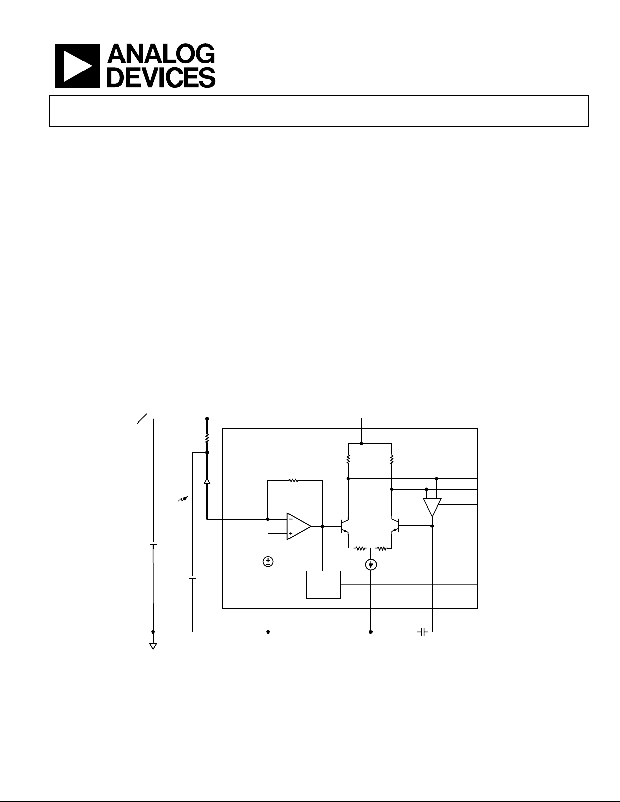
3.3V
R
F
TIA with Average Power Monitor
FUNCTIONAL BLOCK DIAGRAM
ADN2820
PRODUCT DESCRIPTION
The ADN2820 is a compact, high performance, 3.3 V power
supply SiGe transimpedance amplifier (TIA) optimized for
10 Gbps Metro-Access and Ethernet systems. It is a single chip
solution for detecting photodiode current with a differential
output voltage. The ADN2820 features low input referred noise
current and high output transimpedance gain, capable of
driving a typical CDR or transceiver directly. A POWMON
output is provided for input average power monitoring and
alarm generation. Low nominal output offset enables dc output
coupling to 3.3 V circuits. The OFFSET control input enables
output slice level adjustment for asymmetric input signals. The
ADN2820 operates with a 3.3 V power supply and is available in
die form.
VCC (1,2,3)
RF = 500Ω
hυ
IN (13)'
C
B
0.85V
C
F
GND (10, 11)
Figure 1. Functional Block Diagram/Typical Operating Circuit
Rev. 0
Information furnished by Analog Devices is believed to be accurate and reliable.
However, no responsibility is assumed by Analog Devices for its use, nor for any
infringements of patents or other rights of third parties that may result from its use.
Specifications subject to change without notice. No license is granted by implication
or otherwise under any patent or patent rights of Analog Devices. Trademarks and
registered trademarks are the property of their respective owners.
50Ω
One Technology Way, P.O. Box 9106, Norwood, MA 02062-9106, U.S.A.
Tel: 781.329.4700
Fax: 781.326.8703 © 2003 Analog Devices, Inc. All rights reserved.
A
V
50Ω
= 20dB
GND (4,7)
OUT (5)
OUTB (6)
OFFSET (14)
20mA
POWMON (8)
CLF (9)
CLF
www.analog.com
03194-0-001
Page 2

ADN2820
TABLE OF CONTENTS
Specifications..................................................................................... 3
Absolute Maximum Ratings............................................................ 4
ESD Caution.................................................................................. 4
Pad Layout and Functional Descriptions ......................................5
Pad Layout..................................................................................... 5
Die Information............................................................................ 5
Pad Descriptions........................................................................... 5
Pad Coordinates ........................................................................... 5
Typical Performance Characteristics .............................................6
REVISION HISTORY
Revision 0: Initial Version
Applications........................................................................................8
Optical Sensitivity .........................................................................8
Optical Power Monitor.................................................................8
Output Offset Adjust Input..........................................................9
Low Frequency Transimpedance Cutoff Capacitor Selection.9
Bandwidth versus Input Bond Wire Inductance.................... 10
Bandwidth versus Output Bond Wire Inductance................. 10
Butterfly Package Assembly...................................................... 11
Outline Dimensions....................................................................... 12
Ordering Guide .......................................................................... 12
Rev. 0 | Page 2 of 12
Page 3

ADN2820
SPECIFICATIONS
Table 1. Electrical Specifications
Parameter Conditions
DYNAMIC PERFORMANCE
Bandwidth
Total Input RMS Noise
1, 2
1, 2
–3 dB 7.5 9 GHz
DC to 10 GHz 1.0 µA
Small Signal Transimpedance 100 MHz 4000 5000 6000 V/A
Transimpedance Ripple2 100 MHz to 3 GHz ±0.5 dB
Group Delay Variation2 100 MHz to 3 GHz ±10 ps
100 MHz to 9 GHz ±30 ps
Total Peak-to-Peak Jitter
2, 3
I
IN,P-P
Low Frequency Cutoff CLF = 0.1 µF 12 kHz
S22 DC – 10 GHz, differential –10 dB
Linear Input Range Peak-to-peak, <1 dB compression 0.15 mA
Input Overload Current
1, 2
ER = 10 dB 1.4 2.8 mA p-p
ER = 4 dB 1.0 1.9 mA p-p
Maximum Output Swing Differential, I
DC PERFORMANCE
Power Dissipation 147 200 264 mW
Input Voltage 0.75 0.85 0.93 V
Output Common-Mode Voltage DC terminated to VCC VCC – 0.3 V
Output Offset I
IN, AVE
Offset Adjust Sensitivity See Figure 3 120 mV/V
Offset Adjust Range See Figure 3 240 mV
POWMON Sensitivity I
POWMON Offset I
IN, AVE
IN, AVE
1
Min/Max VCC = 3.3 V ± 0.3 V, T
2
Photodiode capacitance CD = 0.22 pF ± 0.04 pF; photodiode resistance = 20 Ω; CB = CF = 100 pF; RF = 100 Ω; input wire bond inductance LIN = 0.5 nH ± 0.15 nH; output
bond wire inductance L
–12
3
10
BER, 8 dB extinction ratio, 0.85 A/W PIN responsivity.
OUT, OUTB
= –15°C to +85°C; Typ VCC = 3.3 V, T
AMBIENT
= 0.85 nH ± 0.15 nH; load impedance = 50 Ω (each output, dc- or ac-coupled).
1
Min Typ Max Unit
= 2.5 mA 17 ps
= 2.0 mA 0.88 1.1 V p-p
IN P-P
< 0.1 mA –20 ±3 +20 mV
= 10 µA to 1 mA 0.76 1 1.2 V/mA
= 0 µA 20 mV
= 25°C.
AMBIENT
Rev. 0 | Page 3 of 12
Page 4

ADN2820
ABSOLUTE MAXIMUM RATINGS
Table 2. ADN2820 Absolute Maximum Ratings
Parameter Rating
Supply Voltage (VCC to GND) 5.2 V
Internal Power Dissipation
Output Short Circuit Duration Indefinite
Maximum Input Current 5 mA
Storage Temperature Range –65°C to +125°C
Operating Ambient Temperature Range –15°C to +85°C
Maximum Junction Temperature 165°C
Die Attach Temperature (<60 seconds) 450°C
ESD CAUTION
ESD (electrostatic discharge) sensitive device. Electrostatic charges as high as 4000 V readily
accumulate on the human body and test equipment and can discharge without detection. Although
this product features proprietary ESD protection circuitry, permanent damage may occur on devices
subjected to high energy electrostatic discharges. Therefore, proper ESD precautions are
recommended to avoid performance degradation or loss of functionality.
Stresses above those listed under Absolute Maximum Ratings
may cause permanent damage to the device. This is a stress
rating only; functional operation of the device at these or any
other conditions above those indicated in the operational
section of this specification is not implied. Exposure to absolute
maximum rating conditions for extended periods may affect
device reliability.
Rev. 0 | Page 4 of 12
Page 5

ADN2820
PAD LAYOUT AND FUNCTIONAL DESCRIPTIONS
PAD LAYOUT DIE INFORMATION
1
VCC VCC VCC
14
OFFSET
13
IN
23
GND
0,0'
OUT
4
5
Die Size
0.875 mm × 1.060 mm
Die Thickness
12 mils = 0.3 mm
Passivation Openings
0.08 mm × 0.08 mm
12
TEST
OUTB
6
0.12 mm × 0.08 mm
0.08 mm × 0.12 mm
11
GND
GND
10
Figure 2. ADN2820 Pad Layout
CLF
9
GND
POWMON
8
7
03194-0-002
Passivation Composition
5000 Å Si3N4 (Top)
+5000 Å SiO
(Bottom)
2
Pad Composition
Al/1% Cu
Backside Contact
P-Type Handle (Oxide Isolated from Active Circuitry)
PAD DESCRIPTIONS
Table 3. Pad Descriptions
Pin No. Pad Function
1–3 VCC Positive Supply. Bypass to GND with a 100 pF or greater single-layer capacitor.
4, 7, 10, 11 GND Ground.
5 OUT Positive Output. Drives 50 Ω termination (ac or dc termination).
6 OUTB Negative Output. Drives 50 Ω termination (ac or dc termination).
8 POWMON
Input Average Power Monitor. Analog signal proportional to average optical input power. Leave open if
unused.
9 CLF Low Frequency Cutoff Setpoint. Connect with a 0.1 μF capacitor to GND for 20 kHz.
12 TEST Test Pad. Leave Floating.
13 IN
Current Input. Bond directly to reverse biased PIN or APD anode. Filter PIN or APD anode with 100 pF × 100 Ω
or greater.
14 OFFSET
Output Offset Adjust Input. Leave open if not being used and the input slice threshold will automatically be set
to the eye center.
PAD COORDINATES
Table 4. Pad Coordinates
Pin
No. PAD X (mm) Y (mm)
1 VCC –0.20 0.45
2 VCC 0.00 0.45
3 VCC 0.20 0.45
4 GND 0.35 0.30
5 OUT 0.35 0.10
6 OUTB 0.35 –0.10
7 GND 0.35 –0.30
Pin
No. PAD X (mm) Y (mm)
8 POWMON 0.20 –0.45
9 CLF 0.00 –0.45
10 GND –0.20 –0.45
11 GND –0.35 –0.30
12 TEST –0.35 –0.10
13 IN –0.35 0.10
14 OFFSET –0.35 0.30
Rev. 0 | Page 5 of 12
Page 6

ADN2820
TYPICAL PERFORMANCE CHARACTERISTICS
0.25
0.20
0.15
0.10
0.05
0
–0.05
DIFFERENTIAL (V)
–0.10
OUT
V
–0.15
–0.20
–0.25
0 0.3 0.6 0.9 1.2 1.5 1.8 2.1 2.4 2.7 3.0 3.3
OFFSET CONTROL INPUT (V)
Figure 3. V
Differential vs. OFFSET Adjust
OUT
10
03194-0-008
–10
–15
–20
–25
–30
|s22| (dB)
–35
–40
–45
–50
0.01 0.1 1
FREQUENCY (GHz)
Figure 6. Differential S22 vs. Frequency
1200
1000
03194-0-011
1
(V)
POWMON
V
0.1
0.001
101 100 1k 10k
I
(µA)
IN
Figure 4. V
POWMON
vs. I
IN
CH1 S21 LOG 5dB/REF 0dB 2:11.571dB 8.156 326 057GHz
CH1 MARKERS
1:14.563 dB
100.000 MHz
1
2
03194-0-009
800
600
400
200
DIFFERENTIAL OUTPUT VOLTAGE (mV p-p)
0
1.0 1.50 0.5 2.0 2.5 3.0
INPUT CURRENT (mA p-p)
Figure 7. Output Voltage vs. Input Current
80
75
70
65
GAIN (dB Ω)
Z
T
60
55
03194-0-012
START .050 000 000GHz STOP 20.000 000 000GHz
Figure 5. ADN2820 S21
03194-0-010
Rev. 0 | Page 6 of 12
50
1.0 1.50 0.5 2.0 2.5 3.0
INPUT CURRENT (mA p-p)
Figure 8. Transimpedance Gain vs. Input Current
03194-0-013
Page 7

ADN2820
40
35
30
25
20
15
TOTAL JITTER p-p (ps)
10
5
0
1.0 1.50 0.5 2.0 2.5 3.0
AVERAGE CURRENT (mA)
Figure 9. Total Jitter Peak-to-Peak vs. Average Input Current (I
60
50
40
30
20
TOTAL JITTER p-p (ps)
10
0
1.0 1.50 0.5 2.0 2.5 3.0
INPUT AMPLITUDE p-p (mA)
Figure 10. Total Jitter Peak-to-Peak vs. Input Amplitude (ER = 10 dB)
= 2 mA p-p)
IN
03194-0-014
03194-0-015
Figure 11. Electrical Eye Diagram at 10 Gbps, PRBS 2
Figure 12. Electrical Eye Diagram at 10 Gbps, PRBS 2
31
with IIN = 100 µA p-p
31
with IIN = 2.5 mA p-p
03194-0-016
03194-0-017
Rev. 0 | Page 7 of 12
Page 8

ADN2820
APPLICATIONS
OPTICAL SENSITIVITY
10
log10)(
=
dBmySensitivit
TSRMS
where:
ρ = photodiode responsivity (A/W), 0.85 A/W typical
= TIA input referred noise (A), typically 1.05 µA for the
I
RMS
ADN2820
α = BER factor, α = 14.1 for 10–12 BER
ER = extinction ratio, 8 dB typical
= PA/CDR input sensitivity (V), 5 mV to 100 mV
V
S
= TIA transimpedance (V/A), 5 kΩ for ADN2820
Z
T
Table 5. Optical Sensitivity
Transimpedance (ZT)
Optical Input Sensitivity (dBm)
PA/CDR
Input
Sensitivity (V
)
S
100 mV –13.1 –15.7 –19.3
50 mV
25 mV
10 mV
5 mV
2 kΩ 5 kΩ Infinite
–15.1 –17.1 –19.3
–16.7 –18.1 –19.3
–18.1 –18.8 –19.3
–18.7 –19.0 –19.3
OPTICAL POWER MONITOR
Average optical power monitor (OPM) measurement is a
recommended diagnostic feature in module multisource
specification agreements (MSAs) such as the 300-pin 10 Gb
transponder (MSA300) and 10 Gb form factor pluggable
module (XFP) specifications.
The ADN2820 enables the simple calculation of OPM using the
POWMON output, which is linearly proportional to the average
input current. When monitoring the POWMON output,
connect to a high impedance input; typical POWMON output
impedance is 1 kΩ. To disable the POWMON feature, leave the
pad floating (not bonded).
ER
×+×+α×
)1(2
−ρ
From a POWMON measurement, the average input power can
be estimated by calculating the optical power monitor (OPM):
)/1000()1()/(
WmWERZVI
OPM (W) = (POWMON (V) – POWMON
× POWMON
GAIN
(V/A))
(V))/(ρ (A/W)
OFFSET
OPM calculation from typical ADN2820 POWMON versus
I
measurement data:
IN,AVE
(POWMON
0
–5
–10
–15
OPM (dBm)
–20
–25
–30
1.0
0.6
0.2
–0.2
= 20 mV, POWMON
OFFSET
–20 –15–30 –25 –10 –5 0
AVERAGE INPUT POWER (dBm)
Figure 13. POWMON Transfer Function
= 1 V/mA, ρ =1 A/W)
GAIN
03194-0-001
Assuming linear diode responsivity ρ, average input current is
linearly proportional to average input power:
(A) = ρ (A/W) × P
I
IN,AVE
IN,AVE
(W)
Ideally,
POWMON (V) = ρ (A/W) × P
POWMON
(V/A) + POWMON
GAIN
IN,AVE
(W) ×
OFFSET
(V)
Rev. 0 | Page 8 of 12
–0.6
OPM MEASUREMENT ERROR (dB)
–1.0
–20 –15–30 –25 –10 –5 0
AVERAGE INPUT POWER (dBm)
Figure 14. POWMON Accuracy
03194-0-002
Page 9

ADN2820
OUTPUT OFFSET ADJUST INPUT
Long reach optical links may suffer from unbalanced 1 and 0
signal shaping due to dispersion and/or optical or avalanche
amplification noise. The ADN2820 enables the user to adjust
the input-referred slice level by adjusting the output offset with
the ADN2820’s outputs dc-coupled.
With the OFFSET pad open (not bonded), the average output
voltage offset [OUT – OUTB] is internally balanced to be less
than ±5 mV. When externally driven by a voltage source, the
ADN2820 average output voltage offset [OUT – OUTB] is
linearly proportional to an applied OFFSET input voltage:
Applied Offset (V) = (OFFSET (V) – ~1.6 V) × OFFSET
where:
OFFSET = voltage applied to the OFFSET pad
GAIN
(mV/V)
LOW FREQUENCY TRANSIMPEDANCE CUTOFF CAPACITOR SELECTION
Digital encoding methods may generate long strings of 1s or 0s,
requiring the transimpedance amplifier pass band to extend to
1 MHz or below. To accommodate this requirement, the
ADN2820 has –3 dB low frequency transimpedance cutoff set
by external capacitor C
the typical –3 dB low frequency transimpedance cutoff can be
estimated by the equation
Because C
is not part of the 10 Gbps signal chain, it is not
LF
required to be a high frequency capacitor type. A ceramic
capacitor is recommended.
100M
. For CLF, values greater than 1000 pF,
LF
f
~ 2 kHz × (1 µF/CLF)
–3dB
OFFSET
With transimpedance, T
= 120 mV/V
GAIN
, the input referred slice adjust can be
Z
calculated from the following equation:
Input Slice Adjust = 1/TZ × (OFFSET (V) – ~1.6 V) × OFFSET
50
40
30
20
10
0
–10
–20
–30
INPUT REFERRED SLICE ADJUST (µA)
–40
–50
0 0.3 0.6 0.9 1.2 1.5 1.8 2.1 2.4 2.7 3.0
OFFSET CONTROL INPUT (V)
Figure 15. Input Slice Adjust vs. OFFSET Calculation Using Typical
[OUT,OUTB] vs. OFFSET Measurement Data
GAIN
(mV/V))
03194-0-003
10M
1M
100k
10k
–3dB LOW FREQUENCY CUTOFF (Hz)
Z
T
1k
Figure 16. Low Frequency Transimpedance Cutoff vs. C
0.1nF 1nF1pF 10pF 10nF 0.1µF1µF
EXTERNAL CLF CAPACITANCE VALUE
Capacitance Using
LF
Typical Data with a 0.1 µF Ceramic Capacitor and Simulation Results with
1 pF to 1 µF Capacitance
03194-0-004
Rev. 0 | Page 9 of 12
Page 10

ADN2820
BANDWIDTH VERSUS INPUT BOND WIRE INDUCTANCE
The ADN2820’s –3 dB bandwidth (BW) is a strong function of
input (IN) bond wire inductance (L
peaks near and falls rapidly after the resonant frequency of the
input bond wire inductance and photodiode capacitance
) ~ 1/(2π × √(LIN × CD)).
(C
D
Table 6. Simulated ADN2820 –3 dB BW vs. L
LIN (nH) –3 dB Bandwidth (GHz)
0 7.4
1 9.0
2 7.8
3 7.0
76
75
74
73
72
71
70
69
TRANSIMPEDANCE (dB Ω)
SIMULATED DIFFERENTIAL
68
67
66
Figure 17. Simulated Differential Transimpedance (dB) vs. Frequency (Hz)
with 0 nH, 1 nH, 2 nH, and 3 nH L
Note: L
OUT
, L
OUTB
Recommendation: L
3nH
0nH
10.1 10 100
FREQUENCY (GHz)
= 1 nH, CD = 0.22 pF.
× CD = 1 nH × 0.22 pF.
IN
). The maximum BW
IN
IN
2nH
1nH
Inductance
IN
03194-0-005
BANDWIDTH VERSUS OUTPUT BOND WIRE INDUCTANCE
The ADN2820 –3 dB bandwidth (BW) depends strongly on the
output (OUT, OUTB) inductance values (L
output inductance greater than 2 nH, the BW is dominated by
, L
the output L
= RL = 50 Ω are the nominal single-ended output resistance
R
O
OUT
/(RO + RL) settling time constant, where
OUTB
and load impedance.
Table 7. Simulated ADN2820 –3 dB BW vs L
L
, L
OUT
(nH) –3 dB Bandwidth (GHz)
OUTB
0 9.1
1 9.0
2 7.5
3 5.9
TRANSIMPEDANCE (dB Ω)
SIMULATED DIFFERENTIAL
76
75
74
73
72
71
70
69
68
67
66
3nH
10.1 10 100
1nH
2nH
FREQUENCY (GHz)
Figure 18. Simulated Differential Transimpedance (dB) vs. Frequency (Hz)
with 0 nH, 1 nH, 2 nH, and 3 nH L
OUT
Note: LIN = 1 nH, CD = 0.22 pF.
, L
Recommendation: L
OUT
OUTB
≤ 1 nH
0nH
, L
OUTB
, L
OUT
OUTB
OUT
inductance
, L
). With
OUTB
03194-0-006
Rev. 0 | Page 10 of 12
Page 11

ADN2820
BUTTERFLY PACKAGE ASSEMBLY
OFFSET
Rf
Cf
PD
V
CC
7.5mm
Cb
OUT
OUTB
C
lf
POWMON
5mm
2.5mm
0mm
03194-0-007
Figure 19. Butterfly Package
Table 8. Bill of Materials
Qty. Description Source
PD 1 VENDOR SPECIFIC (0.5 mm × 0.5 mm) 10 Gbps Photodiode
TIA 1 ADN2820 (0.87 mm × 1.06 mm) Analog Devices SiGe 10 Gbps Transimpedance Amplifier
C
2 GM250X7R10216 (0.5 mm × 0.5 mm) Murata 1000 pF Ceramic Single Layer Capacitor
B
C
1 GM260Y5V104Z10 (0.8 mm × 0.8 mm) Murata 0.1 µF Ceramic Single Layer Capacitor
LF
C
1 D20BV201J5PX (0.5 mm × 0.5 mm) DiLabs 100 pF RF Single Layer Capacitor
F
RF 1 WMIF0021000AJ (0.4 mm × 0.5 mm) Vishay 100 Ω Thin Film Microwave Resistor
Rev. 0 | Page 11 of 12
Page 12

ADN2820
OUTLINE DIMENSIONS
1
14
13
SINGLE PAD SIZE: 0.080 mm x 0.080 mm
(pads 1, 2, 3, 5, 6, 8, 9, 12, 13, 14)
12
DOUBLE PAD SIZE: 0.120 mm x 0.080 mm
(pads 4, 7, 10, 11)
11
10
23
ADN2820
9
0.875 mm
8
4
5
6
7
0.30 mm
1.060 mm
Figure 20. 14-Pad Bare Die
Dimensions shown in millimeters
ORDERING GUIDE
Model Temperature Range Package Description
ADN2820ACHIPS –25°C to +85°C Die Form
© 2003 Analog Devices, Inc. All rights reserved. Trademarks and
registered trademarks are the property of their respective owners.
C03194–0–10/03(0)
Rev. 0 | Page 12 of 12
 Loading...