

Page 1
Information furnished by Analog Devices is believed to be accurate and
Analog Devices for its
use; nor for any infringements of patents or other rights of third parties which
may result from its use. No license is granted by implication or otherwise
Multi -
Rate to 2.7Gb p s Clock and Data
Recovery IC with Limi tin g Amp li fi er
CF
Loss of lock
a
Pr eli m i n ary Tech ni c al Data ADN2809
FEATURES
Meets SONET Requ i r ement s for Jitt er Transf er /
Generatio n / Tolerance
Quantizer Sensitiv i ty: 6 mV typi cal
• Adju st able Slice Level: +/- 100 mV
• 1.9GHz minimum Bandwi dt h
Loss of Sign al Detect Range: 4mV to 17mV
Single Reference Clock Frequenc y fo r all rates
Inc l udin g 15/14 (7%) Wrapp er Rate
• Cho ice of 19.44, 38.88, 77.76 or
155.52MHz
LVPECL / LVDS / LVCMOS / LVTTL compati ble
inp u t s (LVPECL / L VDS only at 155.52 MHz)
19.44MHz Cryst al Osci ll ato r fo r Mod u le apps
Loss of Lock indicator
Loop b ack mo d e for High Speed Test Data
Output Squelch & Cloc k Recovery Func tio n s
Single Suppl y Operatio n: 3.3 Volts (+
Low Power: 780 mW Typical
Patented Clock Recovery Archit ectu re
7 x 7 mm 48 pin L FCSP
APPLICATIONS
SONET OC-3/12/48, SDH STM-1/4/16, and all
asso c i ated FEC rates
WDM transpon ders
SONET/SDH regenerato rs and test equi p m ent
Backplane application s
10%)
PRODUCT DESCRIP TI O N
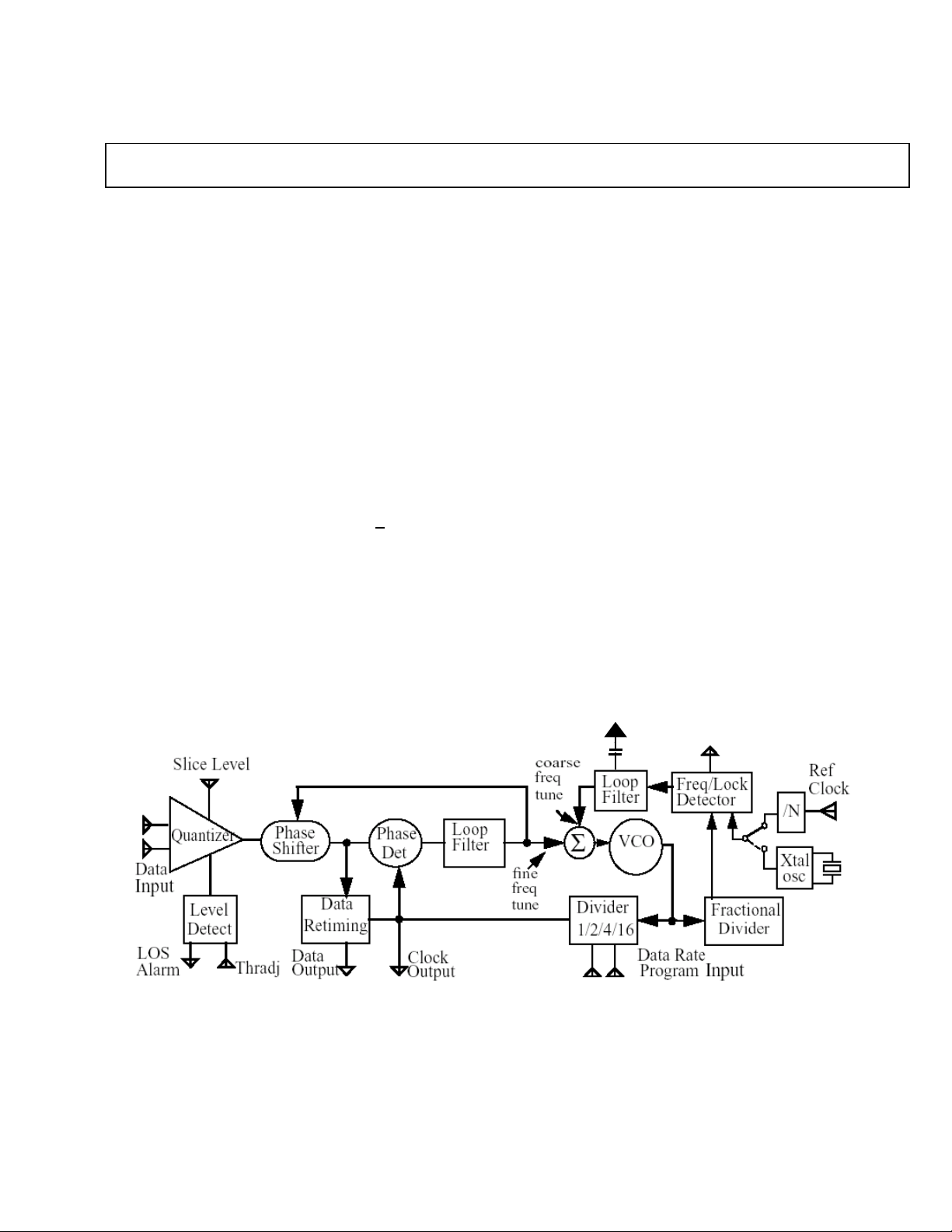
The ADN2809 provides the receiver functions of Quantization,
Signal Level Detect and Clock and Data Recovery at rates of
OC-3, OC-12, Gigabit Ethernet, OC-48 and all FEC rates. All
SONET jitter requirements are met, including: Jitter Transfer;
Jitter Generation; and Jitter Tolerance. All specifications are
quoted for -40 to 85C ambient temperature unless otherwise
noted.
The device is intended for WDM system applications and can be
used with either an external reference clock or an on-chip
oscillator crystal. Both native rates and 15/14 rate digital
‘wrappers’ rates are supported by the ADN2809, without any
change of reference clock required.
This device together with a PIN diode and a TIA preamplifier
can implement a highly integrated, low cost, low power fiber
optic receiver.
The receiver front end Signal Detect circuit indicates when the
input signal level has fallen below a user adjustable threshold.
The ADN2809 is available in a compact 48 pin chip scale
package.
REV. PrB Sept 2001
reliable. However, no responsibility is assumed by
under any patent or patent rights of Analog Devices.
Fun ctional Block Diagram
One Technolog y Way, P.O. Box 9106,
Tel: 781/329-4700 www.analog.com
Fax: 781/326-8703 ©Analog Devi c es, Inc., 2001
Norwo o d, MA 02062-9106 U.S.A.
Page 2

ADN2809
Para meter
JITTER TOLERANCE TRACKING BANDWIDTH
ADN2809 ELECTRICAL CHARACTERISTICS at T
QUANTIZE R–DC CHARACTERI STICS
Input Voltage Range
Input Common Mode Voltage
Input Peak-to-Peak Differential Voltage
Input Sensitivity, V
Input Overdrive, V
(Peak-to-Peak Differential)
SENSE
OD
Input Maximum Offset Voltage
Input Current
Input RMS Noise
QUANTIZE R-AC CHARACTERI STICS
Upper –3 dB Bandwidth
Small Signal Gain
S11 Maximum @ 2.5GHz, Figure 7
Input Resistance
Input Capacitance
Pulse Width Distortion
QUANTIZ E R SLIC E ADJUSTMENT
Gain (Threshold/Vin)
Control Voltage Range
Control Voltage Range
Slice Threshold Offset
LEVEL DETECT
Level Detect Range (See Figure 4)
Response Time
Hysterises (Electrical), AC Coupled Signal
SDOUT output Logic High
SDOUT output Logic Low
Level Detect Output is a logic “1” LVCMOS
Compatible with no signal present.
POWER SUPPLY VOLTAGE POWER SUPPLY CURRENT PHASE-LOCKED LOOP CHARACTERISTICS
JITTER TRANSFER BANDWIDTH
(See Figure 5 and Table 1)
(See Figure 5 and Table 1)
JITTER TOLERANCE (OC-48)
to T
, VCC=V
to V
A=TMIN
MAX
, VEE=0V, CF=4.7µF, 20 ohm ESR for xo unless otherwise noted
MIN
MAX
Conditions Min Typ Max Units
Single Ended, DC Coupled @ PINor N
“
PINor N
@
AC Coupled I/P
IN
PIN- NIN, Figure 2, BER= <1 x 10
Figure 3, BER = <1 X 10
1
-10
-10
SliceP, SliceN = VCC
-10
1 X 10
BER = <
Differential
Single-Ended
Vin = SliceP-SliceN
SliceP-SliceN
SliceP or SliceN
Full input range
= 0Ω
R
THRESH
R
= 10kΩ
THRESH
R
= 200kΩ
THRESH
DC Coupled
= 0Ω
R
THRESH
R
= 10kΩ
THRESH
R
= 200kΩ
THRESH
Load = +2mA (
Load = -2mA (
to V
V
MIN
to V
V
MIN
NOTE: SONET SPECS APPEAR IN
BOLD
ADN2812 Sources I)
ADN2812 Sinks I)
MAX
MAX
OC-48
Gigabit Ethernet
OC-12
OC-3
OC-48
Gigabit Ethernet
OC-12
OC-3
600 Hz
6 KHz
100 MHz
1 MHz
IN
0
0.4
1.2
1.2
2.4
10
5
6
3
0.5
10
244
µVrms
1.9
54
-15
50
0.65
10
0.131
-0.8
1.3
-1.0
2
6
15
0.1
2.7
3
8.8
17
3
5
5
5
3
0.2
0.134
0.8
VCC
1.0
4
12
21
5
7
7
7
0.4
3.0 3.6 V
140 236 380 mA
1.0
0.5
0.25
0.065
370
185
93
23
4.8
4.8
4.8
4.8
80
>20
5.5
>0.6
2
2
2000
1000
500
130
MHz
MHz
MHz
MHz
UIp-p
UIp-p
UIp-p
UIp-p
V
V
V
mV
mV
mV
µA
GHz
dB
dB
Ω
pF
ps
V/V
V
V
mV
mV
mV
mV
µs
dB
dB
dB
V
V
KHz
KHz
KHz
KHz
JITTER GENERATION
(12kHz to 20MHz)
(12kHz to 10MHz)
(12kHz to 5MHz)
(12kHz to 1.3MHz)
OC-48
Gigabit Ethernet
OC-12
OC-3
REV. PrB Oct. .2001 - 2 -
0.003
0.03
0.003
0.03
0.003
0.03
0.003
0.03
0.01
0.1
0.01
0.1
0.01
0.1
0.01
0.1
UI rms
UIp-p
UI rms
UIp-p
UI rms
UIp-p
UI rms
UIp-p
Page 3
Para meter
JITTER PEAKING MAXIMUM
ADN2809 ELECTRICAL CHARACTERISTICS at T
CML OUTPUT FORMAT
Single-Ended Output Voltage Swing V
Differential Output Voltage Swing V
Rise Time (t
Fall Time (t
)
R
)
F
DIFF
ADN2809
to T
, VCC=V
to V
A=TMIN
MAX
Conditions Min Typ Max Units
OC-48
Gigabit Ethernet
OC-12
OC-3
SE
See Figure 2 and Figure 6
See Figure 2 and Figure 6
20% - 80%
80% - 20%
, VEE=0V, CF=4.7µF, 20 ohm ESR for xo unless otherwise noted
MIN
MAX
0.1
0.1
0.1
0.1
300
600
430
860
550
1100
150
150
dB
dB
dB
dB
mV
mV
pS
pS
Output High Voltage V
Output Low Voltage V
OH
OL
Data Setup Time T
(Figure 1)
S
Data Hold Time T
(Figure 1)
H
TEST DATA DC CHARACTERI STI CS
Input Voltage Swing V
(Figure 2)
SE
Input Voltage Range
LVTTL DC CHARACTERISTICS
Output High Voltage
V
OH
Output Low Voltage
V
OL
Input High Voltage
V
IH
Input Low Voltage
V
IL
Input High Current
I
IH
Input Low Current
I
IL
REFCL K DC CHARACTE RISTICS
Input Voltage Swing V
(Figure 2)
SE
Input Voltage Range
Note: (1) Recommended for Optimum Sensitivity.
Note: (2) Equipment Limitation.
Figure 6
Figure 6
OC48
Gigabit Ethernet
OC12
OC3
OC48
Gigabit Ethernet
OC12
OC3
Single-Ended
Single-Ended
= -100uA (ADN2809 Sources I)
I
OH
= 1.0mA (ADN2809 Sinks I)
I
OL
Vin = +2.4 V @ +25C
Vin = +0.5 V @ +25C
Single-Ended
Single-Ended
VCC-0.55
150
350
750
3150
150
350
750
3150
0.06
2.3
2.4
2.0
-500
0.032
0
VCC
VCC-0.32
0.8
VCC+0.4
0.5
0.8
50
VCC
VCC
V
V
pS
pS
pS
pS
pS
pS
pS
pS
V
V
V
V
V
V
µA
µA
V
V
ABSOL UTE M AXIMUM RATINGS
Supply Voltage.............................................................. ...+8 V
Input Voltage (pin x or pin xto Vcc).... ........................... .TBD
Maximum Junction Temperature..............................165 deg C
Storage Temperature Range.............. -65 deg C to +150 deg C
Lead Temperature (Soldering 10 sec).. ....................300 deg C
ESD Rating (human body model)....... ........................... ..TBD
Stress above those listed under "Absolute Maximum Ratings" may cause permanent damage
to the device. This is a stress rating only and functional operation of the device at these or any
other conditions above those i ndicated in the operational sections of this s pecification is not
implied. Exposure to absolute maximum rating conditions for extended periods may affect
device reliability.
REV. PrB Oct. .2001 - 3 -
ORDERI NG GUIDE
MODEL TEMP
RANGE
ADN2809XCP -40/+85oC LFCSP-16 CP-16
ADN2809XCP-RL -40/+85oC
Package
Descript-ion
LFCSP-16
2500 Pieces
Option
CP-16
Page 4
ADN2809
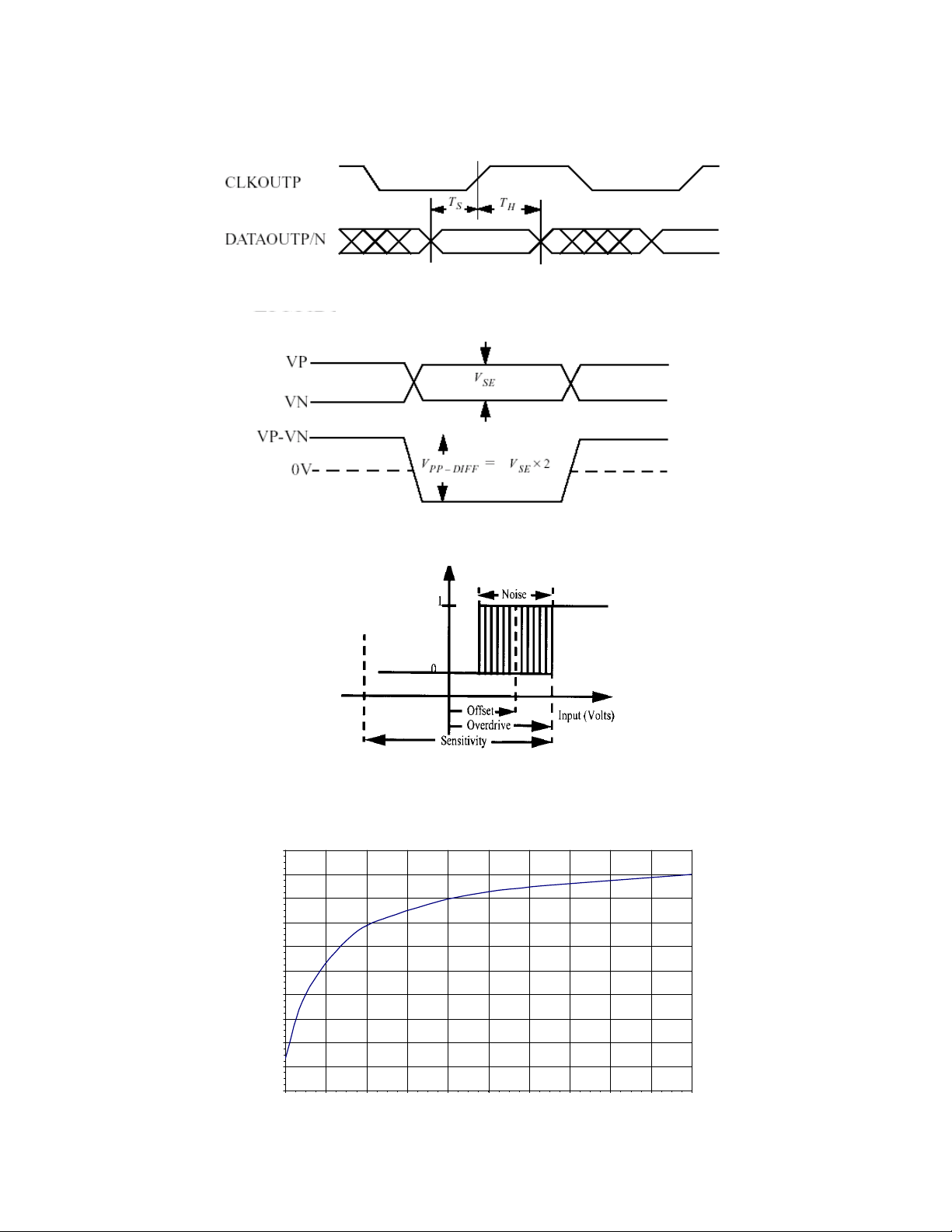
Figure 2. Signal Level Definition
OC-48 2^ 23 LOS Curv e
RThresh
LOS Trip Voltag e (mV)
Figure 1. Output Timing definitions
REV. PrB Oct. .2001 - 4 -
Figure 3. Quantizer Signal Definitions
20.0
18.0
16.0
14.0
12.0
10.0
8.0
6.0
4.0
2.0
0.0
0 20000 40000 60000 80000 100000 120000 140000 160000 180000 2 00 000
Figure 4. LOS Comparator Trip Point Programming
Page 5

OC3_jit_tolerance
OC12_jit_tolerance
GBE_jit_tolerance
OC48_jit_tolerance
OC3_jit_transfer
OC12_jit_transfer
GBE_jit_transfer
OC48_jit_transfer
-1.5
ADN2809
Jitter Tra nsfer Jitter ToleranceRate
SONET
Spec
OC48 2MHz 370kHz 5.4 1MHz 4.77MHz 4.8
GbE 1MHz 185kHz 5.4 500kHz 4.77MHz 9.6
OC12 500kHz 93kHz 5.4 250kHz 4.77MHz 19.2
OC3 130kHz 23kHz 5.6 65kHz 4.77MHz 73.4
Table I. Typical Jitter Transfer a nd Jitter Tolerance Performance
0
-.5
-1
ADN2809 Margin SONET
spec
ADN2809 Margin
dB
-2
-2.5
-3
-3.5
-4
-4.5
-5
-5.5
-6
-6.5
-7
-7.5
-8
-8.5
-9
REV. PrB Oct. .2001 - 5 -
-9.5
-10
freq, Hertz
1e3 1e4 1e5 1e6 1e7 1e8
Figure 5. Tracking Bandwidth and Jitter Filter ing
Page 6

ADN2809
Figure 6. Recommended AC Output Termination
Figure 7. ADN2809 S11 vs. Frequency
REV. PrB Oct. .2001 - 6 -
Page 7

ADN2809
THEORY OF OPERATION
The ADN2809 is a delay- and phase-locked loop circuit for
clock recovery and data retiming from an NRZ encoded data
stream. The phase of the input data signal is tracked by two
separate feedback loops which share a common control voltage.
A high speed delay- locked loop path uses a voltage controlled
phase shifter to track the high frequency components of input
jitter. A separate phase control loop, comprised of the vco,
tracks the low frequency components of input jitter. The initial
frequency of the vco is set by yet a third loop which compares
the vco frequency with the reference frequency and sets the
coarse tuning voltage. The jitter tracking phase-locked loop
controls the vco by the fine tuning control.
The delay- and phase- loops together track the phase of the input
data signal. For example, when the clock lags input data, the
phase detector drives the vco to higher frequency, and also,
increases the delay through the phase shifter: these actions both
serve to reduce the phase error between the clock and data. The
faster clock picks up phase while the delayed data loses phase.
Since the loop filter is an integrator, the static phase error will be
driven to zero.
Another view of the circuit is that the phase shifter implements
the zero required for frequency compensation of a second order
phase-locked loop, and this zero is placed in the feedback path
and thus, does not appear in the closed-loop transfer function.
Jitter peaking in a conventional second order phase-locked loop
is caused by the presence of this zero in the closed-loop transfer
function. Since this circuit has no zero in the closed-loop
transfer, jitter peaking is minimized.
The delay- and phase- loops together simultaneously provide
wide-band jitter accommodation and narrow-band jitter filtering.
The linearized block diagram in Figure 8 shows the jitter
transfer function , Z(s)/X(s), is a second order low pass
providing excellent filtering. Note the jitter transfer has no zero,
unlike an ordinary second order phase-locked loop. This means
that the main PLL loop has low jitter peaking, see Figure 9. This
makes this circuit ideal for signal regenerator applications where
jitter peaking in a cascade of regenerators can contribute to
hazardous jitter accumulation.
The error transfer, e(s)/X(s), has the same high pass form as an
ordinary phase-locked loop. This transfer function is free to be
optimized to give excellent wide-band jitter accommodation
since the jitter transfer function, Z(s)/X(s), provides the narrowband jitter filtering. See Figure 5 for a table of error transfer
bandwidths and jitter transfer bandwidths at the various data
rates.
The delay- and phase- loops contribute to overall jitter
accommodation. At low frequencies of input jitter on the data
signal, the integrator in the loop filter provides high gain to track
large jitter amplitudes with small phase error. In this case the
vco is frequency modulated and jitter is tracked as in an ordinary
phase-locked loop. The amount of low frequency jitter that can
be tracked is a function of the vco tuning range. A wider tuning
range gives larger accommodation of low frequency jitter. The
internal loop control voltage remains small for small phase
errors, so the phase shifter remains close to the center of its
range and thus contributes little to the low frequency jitter
accommodation.
At medium jitter frequencies, the gain and tuning range of the
vco are not large enough to track input jitter. In this case the vco
control voltage becomes large and saturates and the vco
frequency dwells at one or the other extreme of its tuning range.
The size of the vco tuning range, therefore has only a small
effect on the jitter accommodation. The delay-locked loop
control voltage is now larger, and so the phase shifter takes on
the burden of tracking the input jitter. The phase shifter range, in
UI, can be seen as a broad plateau on the jitter tolerance curve .
The phase shifter has a minimum range of 2UI at all data rates.
The gain of the loop integrator is small for high jitter
frequencies, so that larger phase differences are needed to make
the loop control voltage big enough to tune the range of the
phase shifter. Large phase errors at high jitter frequencies cannot
be tolerated. In this region the gain of the integrator determines
the jitter accommodation. Since the gain of the loop integrator
declines linearly with frequency, jitter accommodation is lower
with higher jitter frequency. At the highest frequencies, the loop
gain is very small, and little tuning of the phase shifter can be
expected. In this case, jitter accommodation is determined by the
eye opening of the input data, the static phase error, and the
residual loop jitter generation. The jitter accommodation is
roughly 0.5UI in this region. The corner frequency between the
declining slope and the flat region is the closed loop bandwidth
of the delay-locked loop, which is roughly 3MHz for all data
rates.
REV. PrB Oct. .2001 - 7 -
Page 8

ADN2809
Figure 8. ADN2809 Architecture
Figure 9. ADN2809 Jitter Response vs. Conventional PLL
REV. PrB Oct. .2001 - 8 -
ADN2809
Page 9

ADN2809
FUNCTIONAL DESCRIPT I O N
Limiting Amplifier / Bypass & Loopba ck
The limiting amplifier has differential inputs (PIN/NIN), which
are normally AC coupled to the internal 50 ohm termination
(although DC coupling is possible). Input offset is factory
trimmed to achieve better than 6mV typical sensitivity with
minimal drift. The Quantizer Slicing level can be offset by +/100mV to mitigate the effect of ASE (amplified spontaneous
emission) noise by a differential voltage input of +/-0.8V
applied to ‘SLICEP/N’ inputs. If no adjustment
of the slice level is needed, SLICEP/N should be tied to VCC.
When the ‘Bypass’ input is driven to a TTL high state, the
Quantizer output is connected directly to the buffers driving the
Data Out pins, thus bypassing the clock recovery circuit (Figure
10). This feature can help the system to deal with non standard
bit rates. The loopback mode can be invoked by driving the
‘LOOPEN’ pin to a TTL high state, which facilitates system
diagnostic testing. This will connect the Test inputs (TDINP/N)
to the clock and data recovery circuit (per Figure 10). The Test
inputs can be left floating, when not in use. They accept AC or
DC coupled signal levels, or AC coupled LVDS.
Loss of Signal (LOS) Detector
The receiver front end Signal Detect circuit indicates when the
input signal level has fallen below a user adjustable threshold.
The threshold is set with a single external resistor, as illustrated
in figure 4, which assumes that the slice inputs are inactive.
If the LOS detector is used the Quantizer Slice Adjust pins must
both be tied to VCC, to avoid interaction with the LOS threshold
level. Note that it is not expected to use both LOS and Slice
Adjust at the same time: systems with optical amplifiers need
the slice adjust to evade ASE, but a loss of signal causes the
optical amplifier output to be full scale noise, thus the LOS
would not detect the failure. In this case the Loss of Lock signal
will indicate the failure.
Reference Clock
The ADN2809 can accept any of the following reference clock
frequencies: 19.44 MHz, 38.88MHz, 77.76MHz at
LVTTL/LVCMOS/LVPECL/LVDS levels or 155.52MHz at
LVPECL/LVDS levels via the REFCLKN/P inputs, independent
of data rate (including gigabit ethernet). The input buffer accepts
any differential signal with a peak to peak differential
amplitude of greater than 64mV (e.g. LVPECL or LVDS) or a
standard single ended low voltage TTL input, providing
maximum system flexibility. The appropriate division ratio can
be selected using the REFSEL0/1 pins, according to Table 3.
Phase noise and duty cycle of the Reference Clock are not
critical and 100ppm accuracy is sufficient.
A crystal oscillator is also provided, as an alternative to using
the REFCLKN/P input. Details of the recommended crystal are
given in Table 3.
REFSEL must be tied to VCC when the REFCLKN/P inputs are
active, or tied to VEE when the oscillator is used. No connection
between the XO pin and REFCLK input is necessary (see figure
11). Please note that the crystal should operate in series resonant
mode, which renders it insensitive to external parasitics. No
trimming capacitors are required.
Lock Detector Oper a tion
The lock detector monitors the frequency difference between the
VCO and the reference clock, and de-asserts the ‘Loss of Lock’
signal when the VCO is within 500ppm of center frequency.
This enables the phase loop which then maintains phase lock,
unless the frequency error exceeds 0.1%. Should this occur, the
‘Loss of Lock’ signal is re-asserted and control returns to the
frequency loop which will re-acquire, and maintain a stable
clock signal at the output. The frequency loop requires a single
external capacitor between CF1 and CF2. The capacitor
specification is given in Table 5.
Squelch Mode
REV. PrB Oct. .2001 - 9 -
When the ‘Squelch’ input is driven to a TTL high state, both the
clock and data outputs are set to the zero state, to suppress
downstream processing. If desired, this pin can be directly
driven by the LOS (Loss-Of-Signal) or LOL (Loss-Of-Lock)
detector outputs. If the Squelch function is not required, the pin
should be tied to VEE.
Page 10

ADN2809
Figure 11. Reference Sources
Figure 12. Data Input Terminations
Identical Digits (CID) and amount of
2809
2809
Figure 10. Test Modes
ADN
ADN
Note:
The value of Cin required depends
on the data rate, # Consecutive
Patter Dependent Jitter (PDJ) which
can be tolerated. e.g. for 1000 CID
and <0.01UI pk-pk PDJ, 100nF is
needed at OC48 and 1.6uF at OC3.
REV. PrB Oct. .2001 - 10 -
Page 11

ADN2809
Para meter
TABLE 2. Data R a t e Selection
SEL2 SEL0 SEL1 Rate Fr equency
0 0 0 OC48 2.48832 GHz
0 0 1 Gigabit Ethernet 1.25 GHz
0 1 0 OC12 622.08 MHz
0 1 1 OC3 155.52 MHz
1 0 0 OC48 * 15/14 2.666 GHz
1 0 1 Gigabit Ethernet * 15/14 1.339 GHz
1 1 0 OC12 * 15/14 666.51 MHz
1 1 1 OC3 * 15/14 166.63 MHz
TABLE 3. Reference Frequency Selection
REFSEL1 REFSEL0 Applied Reference Fr equen cy
0 0 19.44 MHz
0 1 38.88 MHz
1 0 77.76 MHz
1 1 155.52 MHz
TABLE 4. Crysta l Specification - see note (3)
Para meter Value
Mode Series Resonant
Frequency / Overall Stability 19.44 MHz / +/- 50 ppm
Frequency Accuracy
Temp. Stability
Ageing
ESR 20 ohms max
(3) No additional external components are required
+/- 50 ppm / total Temp. Stability
TABLE 5. Recommend ed C a p a citor Specificat ion
Value
Capacitance (-40C to 85C) >3.0uF
Leakage (-40C to 85C) <80nA
Rating >6.3V
REV. PrB Oct. .2001 - 11 -
Page 12

ADN2809
ADN2809 PIN DESCRI P T IO N
Pin No. Name I/O Level Descrip t ion
2,26,28, Exposed Pad VCC P 3.3V Analog Power
3,9,27,29, 42 VEE G 0V Analog ground
20,35,36,47 VCC P 3.3V Digital supply
1 THRADJ I/O Analog I/O LOS threshold setting resistor
4 VREGF I/O Analog I/O Reference capacitor
5 PIN I Analog current Differential data signal input
6 NIN I Analog current Differential data signal input
7 SLICEP I Analog voltage Slice level
8 SLICEN I Analog voltage Slice level
10 LOL O LVTTL / LVCMOS High level indicates loss of lock
11 XO O Analog output Crystal oscillator
12 XO O Analog output Crystal oscillator
13 REFCLKN I Any Differential reference clock
14 REFCLKP I Any Differential reference clock
15 REFSEL I LVTTL / LVCMOS Reference source select
17 TDINP I CML Differential test data input
18 TDINN I CML Differential test data input
21 CF1 I/O Analog I/O Frequency loop capacitor
23 REFSEL1 I LVTTL / LVCMOS Reference rate select
24 REFSEL0 I LVTTL / LVCMOS Reference rate select
25 CF2 I/O Analog I/O Frequency loop capacitor
30 SEL2 I LVTTL / LVCMOS Data rate select
31 SEL1 I LVTTL / LVCMOS Data rate select
32 SEL0 I LVTTL / LVCMOS Data rate select
37 DATAOUTN O CML Differential recovered data
38 DATAOUTP O CML Differential recovered data
39 SQUELCH I LVTTL / LVCMOS Disable clock and data outputs
40 CLKOUTN O CML Differential retimed clock
41 CLKOUTP O CML Differential retimed clock
44 BYPASS I LVTTL / LVCMOS Disable clock and data recovery
45 SDOUT O LVTTL / LVCMOS High level indicates loss of signal
48 LOOPEN I LVTTL / LVCMOS Enable high speed test data inputs
ADN2809 PIN CO NFI G UR ATI O N
REV. PrB Oct. .2001 - 12 -
Page 13

ADN2809
Mechanical Out line Dimen sions
Dimensions shown in millimeters and (inches).
REV. PrB Oct. .2001 - 13 -
 Loading...