

Page 1
Mobile TV One-chip Receiver
Preliminary Technical Data
FEATURES
RF Tuner and Demodulator SoC for T-DMB/DAB/FM
Supports Triple-band: Band III, L-Band and FM
Wide Dynamic Range: −102dBm to +5dBm in 50Ω
Low Power Consumption
CSP_BGA Package: 75mW@TDMB_Video_544kbps
CSP Package: 65mW@TDMB_Video_544kbps
Reference Clock
CSP_BGA Package: 16.384/19.2MHz
CSP Package: 16.384MHz
1.2V Supply Voltage for Core and 1.8/2.8V Dual Supply
Voltage selectable for I/O
Supports JTAG I/O Boundary Scan
Fully Compliant to T-DMB Standards in Korea and ETSI
300 401 Physical Layer Definition
Satisfied TTAS.KO-07.0024 Specification of the data
Services for VHF Digital Multimedia Broadcasting
Supports ETSI EN 300 744 (204,188) Outer Coder
144-Ball
Chip Scale Package Ball Grid Array (CSP_BGA) and
92-Ball Chip Scale Package (CSP)
for T-DMB/DAB/FM
ADMTV315
CSP_BGA Package 7mm × 7mm × 1.0mm, 0.5mm pitch
CSP Package 5mm × 5mm × 0.75mm, 0.45mm pitch
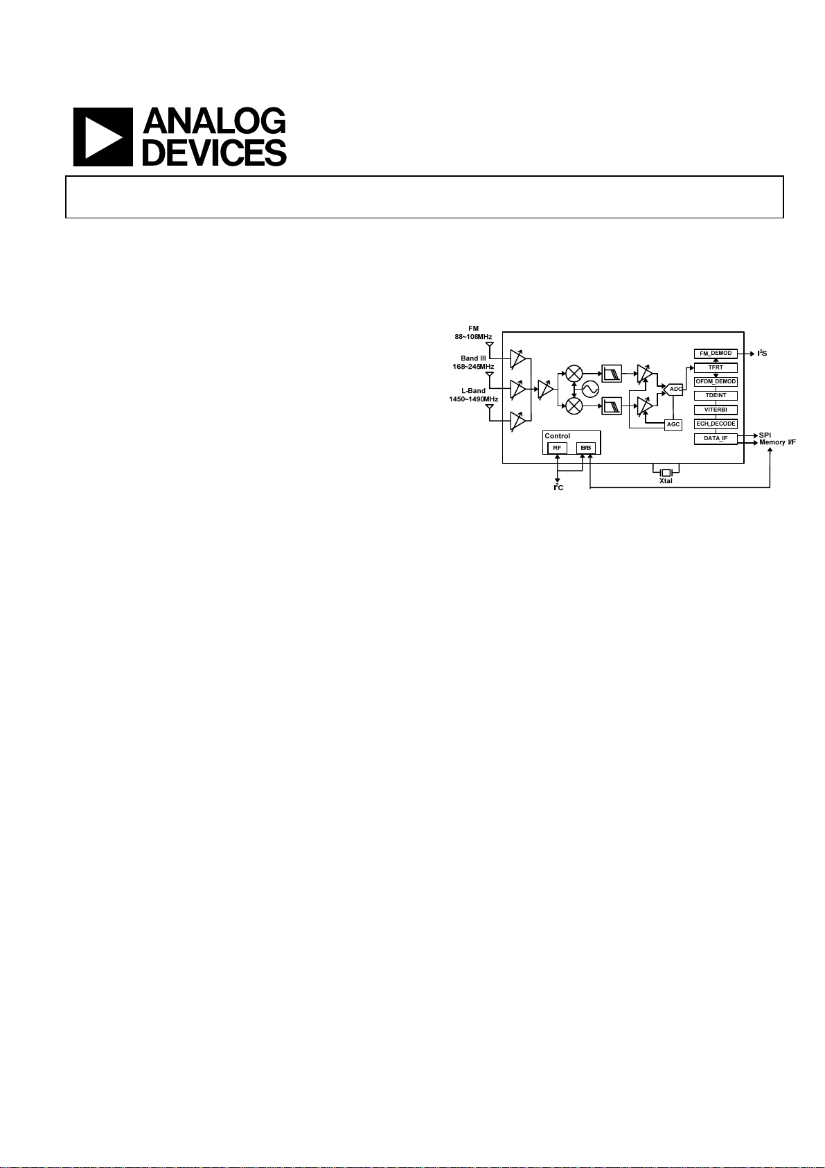
FUNCTIONAL BLOCK DIAGRAM
Figure 1. ADMTV315 Block diagram
GENERAL DESCRIPTION
ADMTV315 is a highly integrated SoC (System-on-Chip) TDMB/DAB receiver, which supports triple bands (Band III, LBand and FM). This device is composed of high performance
RF front-end tuner and OFDM (Orthogonal Frequency
Division Multiplex) demodulator in a small-size single package.
The zero-IF down-conversion RF front-end includes LNA, RF
PGA, mixer, high-resolution fractional-N PLL, on-chip low
phase noise VCO, BB PGA, and automatic cutoff frequencytuning LPF. The baseband of ADMTV315 includes 10bit ADC,
OFDM demodulator and FEC/audio/data decoders. This device
supports various serial interfaces such as I2C, I2S, and SPI to
make interface with external devices more flexible. With good
sensitivity and wide dynamic range, ADMTV315 is the best
solution for T-DMB/DAB application. It is designed to comply
with TTAS.KO-07.0024 specification of the data services for
VHF Digital Multimedia Broadcasting (T-DMB) and ETSI EN
300 401 (European DAB).
The additional features of ADMTV315 are as follows:
z Supports transmission mode 1, 2, 3 and 4
z Supports digital frequency control and timing control
z Supports simultaneous channel reception
- Maximum 64 sub-channels
- 4 enhanced channels (TDMB/ESM/EPM)
z Supports various AP (HOST) interfaces
- SRAM Base parallel interface (control + data)
2
- Serial interface (control: I
C, data: SPI)
- Single SPI interface at PIP mode
z Supports TII reception
z Supports FM reception
z Supports automatic setting with Multiplex Configuration
Information decoder
- CIF counter synchronization
- Multiplex configuration & reconfiguration
- Enhanced channel (TDMB/EPM)
z Supports full capacity channel decoding
z Minimized external components
- No external system memory
- Bit de-interleaver memory included
Rev. PrA
Information furnished by Analog Devices is believed to be accurate and reliable. However, no
responsibility is assumed by Analog Devices for its use, nor for any infringements of patents or other
rights of third parties that may result from its use. Specifications subject to change without notice. No
license is granted by implication or otherwise under any patent or patent rights o f Analog Devices.
Trademarks and registered trademarks are the property of their respective owners.
One Technology Way, P.O. Box 9106, Norwood, MA 02062-9106, U.S.A.
Tel: 781.329.4700
Fax: 781.461.3113 ©2008 Analog Devices, Inc. All rights reserved.
www.analog.com
Page 2

ADMTV315 Preliminary Technical Data
TABLE OF CONTENTS
FEATURES........................................................................................ 1
GENERAL DESCRIPTION ............................................................ 1
REVISION HISTORY ..................................................................... 2
Specifications..................................................................................... 3
Operating Conditions.................................................................. 3
Electrical Charateristics............................................................... 3
Digital Timing Characteristics ................................................... 5
Electrostatic Charateristics.......................................................... 5
Absolute Maximum Ratings............................................................ 6
ESD Caution.................................................................................. 6
Pin Configuration and Function Descriptions............................. 7
Pin Map (BGA Package Type).................................................... 7
Pin Map (ADMTV315ACBZRL WLCSP Package Type)..... 12
Register map of RF part................................................................. 16
Theory of Operation ...................................................................... 23
RF Low Noise Amplifier (LNA), RF Programmable Gain
Amplifier (PGA) and Down-Converter.................................. 23
Local Oscillator (LO) .................................................................23
Phase Locked Loop (PLL) ......................................................... 23
Baseband Low-Pass FIlter (LPF) and Variable Gain Amplifier
(VGA) .......................................................................................... 24
Automatic Gain Control (AGC)............................................... 24
Power-Down Control ................................................................ 24
System Interface.............................................................................. 26
DATA Interface........................................................................... 26
APB Sub-System............................................................................. 43
System Architecture................................................................... 43
Address Map............................................................................... 43
APB Sub-System Components ................................................. 45
Applications..................................................................................... 50
BGA Package Type..................................................................... 50
WLCSP Package Type................................................................ 52
Outline Dimensions....................................................................... 54
BGA Package Type..................................................................... 54
WLCSP Package Type................................................................ 55
REVISION HISTORY
Rev.PrA | Page 2 of 57
Page 3

Preliminary Technical Data ADMTV315
SPECIFICATIONS
OPERATING CONDITIONS
Table 1. Recommended Operating Conditions
Parameter Symbol Min Typ Max Unit
DC Supply Voltage
VDD (1.2 V)
VDD (1.8 V) 1.65 1.95 V
(2.8 V) 2.5 3.3 V
V
DD
V
IN/VOUT
Operating Ambient Temperature T
−40 85 °C
opr
ELECTRICAL CHARATERISTICS
TA = 25°C, all 1.8 V supplies = 1.65 V to 1.95 V, unless otherwise noted.
Table 2. 1.8 V DC Electrical Characteristics
Parameter Condition Symbol Min Typ Max Unit
Input High Current
Input Low Current
Input High Voltage CMOS
Input High Voltage SCMOS
Input Low Voltage CMOS
Input Low Voltage SCMOS
Output High Voltage
Output Low Voltage
Tri-state Output Leakage Current
Normal
V
= VDD
IN
Down Pull - Down
Normal
V
= VSS
IN
Up Pull - Up
= Drive Current VOH
I
OH
= Drive Current VOL
I
OL
= VDD of VSS I
V
OUT
1.1 1.3 V
1.65 1.95 V Input/Output Voltage
2.5 3.3 V
l
IH
−5 5 µA
1 30 µA
l
IL
−5 5 µA
−30 −1 µA
V
IH
V
T+
V
IL
V
T−
0.65×V
0.7×V
0.35×V
0.3×V
V
V
DD
V
DD
DD
V
DD
− 0.45 V
DD
0.45 V
OZ
−10 10 µA
V
T
= 25°C, all 2.8 V supplies = 2.5 V to 3.1 V, unless otherwise noted.
A
Table 3. 2.8 V DC Electrical Characteristics
Parameter Condition Symbol Min Typ Max Unit
Input High Current
VIN = VDD
Pull - Down Down
Input Low Current
VIN = VSS
Pull - Up Up
Input High Voltage CMOS
Input High Voltage SCMOS
Input Low Voltage CMOS
Input Low Voltage SCMOS
Output High Voltage
Output Low Voltage
Tri-state Output Leakage Current
= Drive Current VOH
I
OH
= Drive Current VOL
I
OL
= VDD of VSS I
V
OUT
Normal −5 5 µA
l
IH
5 60 µA
Normal −5 5 µA
l
IL
−60 −5 µA
V
IH
V
T+
V
IL
V
T−
0.65×V
0.7×V
0.35×V
0.3×V
V
V
DD
V
DD
V
DD
V
DD
− 0.45 V
DD
0.45 V
OZ
−10 10 µA
Rev.PrA | Page 3 of 57
Page 4

ADMTV315 Preliminary Technical Data
TA = 25°C, all 1.2 V supplies = 1.1 V to 1.3 V, 2.8 V supplies = 2.7 V to 2.9 V, unless otherwise noted.
Table 4. FM AC Electrical Characteristics
Parameter Symbol Min Typ Max Unit
FM RF frequency range f
FM
RF input impedance ZIN 50
Input VSWR VSWR 2:1 3:1
Sensitivity P
7 dBV
MIN
T
= 25°C, all 1.2 V supplies = 1.1 V to 1.3 V, 2.8 V supplies = 2.7 V to 2.9 V, unless otherwise noted.
A
Table 5. Band III AC Electrical Characteristics
Parameter Symbol Min Typ Max Unit
Band-III RF frequency range f
Band-III
RF input impedance ZIN 50
Input VSWR VSWR 2:1 3:1
Sensitivity @ BER P
Max Input Power @ BER P
Digital Adjacent Chanel Rejection (n+1) ACR
Digital Adjacent Chanel Rejection (n−1) ACR
Far-off (+5 MHz) FO
Far-off (−5 MHz) FO
−102 −97 dBm
MIN
+5 dBm
MAX
33 38 dBc
DN+1
33 38 dBc
DN−1
42 47 dBc
+5MHz
−5MHz
88 108 MHz
Ω
168 245 MHz
Ω
42 47 dBc
= 25°C, all 1.2 V supplies = 1.1 V to 1.3 V, 2.8 V supplies = 2.7 V to 2.9 V, unless otherwise noted.
T
A
Table 6. L-Band AC Electrical Characteristics
Parameter Symbol Min Typ Max Unit
L-Band RF frequency range f
L-Ba nd
RF input impedance ZIN 50
1450 1492 MHz
Ω
Input VSWR VSWR 2:1 3:1
Sensitivity P
Max Input Power P
Digital Adjacent Chanel Rejection (n+1) ACR
Digital Adjacent Chanel Rejection (n−1) ACR
Far-off (+5 MHz) FO
Far-off (−5 MHz) FO
−101 −97 dBm
MIN
0 dBm
MAX
30 33 dBc
DN+1
30 33 dBc
DN−1
40 47 dBc
+5MHz
−5MHz
40 47 dBc
Rev.PrA | Page 4 of 57
Page 5
Preliminary Technical Data ADMTV315
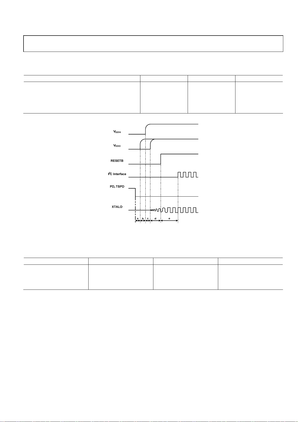
DIGITAL TIMING CHARACTERISTICS
Table 7.
Characteristic Symbol Min Unit
PD Set-up Margin a Don’t Care µs
Power up Set-up Margin for V
Power up Set-up Margin for V
RESETB Set-up Time for RESETB d 100 µs
Set-up Time for I2C Interface e 100 µs
b Don’t Care µs
DD18
c Don’t Care µs
DDIO
Figure 2. Digital Timing Diagram
ELECTROSTATIC CHARATERISTICS
Table 8.
Characteristic HBM MM Remarks
VDD positive > 1000 [V] >100 [V]
VDD negative > 1000 [V] >100 [V]
Vss positive > 1000 [V] >100 [V]
Vss negative > 1000 [V ] >100 [V ]
Rev.PrA | Page 5 of 57
Page 6
ADMTV315 Preliminary Technical Data
ABSOLUTE MAXIMUM RATINGS
TA = 25°C, unless otherwise noted.
Table 9.
Parameter Symbol Rating
DC Supply Voltage
Input/Output Voltage
DC Input Current
Storage Temperature Tstg –65°C to +150°C
VDD (1.2V) 1.7 V
VDD (1.8V) 2.3 V
V
(2.8V) 3.3 V
DD
VIN/V
VIN/V
V
IN/VOUT
L
IN
OUT
OUT
(1.2V)
(1.8V)
(2.8V)
1.7 V
2.3 V
3.3 V
±200mA
Stresses above those listed under Absolute Maximum Ratings may
cause permanent damage to the device. This is a stress rating
only; functional operation of the device at these or any other
conditions above those indicated in the operational section of this
specification is not implied. Exposure to absolute maximum
rating conditions for extended periods may affect device
reliability.
Only one absolute maximum rating may be applied at any one
time.
ESD CAUTION
Rev.PrA | Page 6 of 57
Page 7
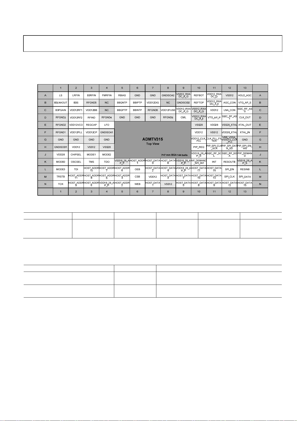
Preliminary Technical Data ADMTV315
PIN CONFIGURATION AND FUNCTION DESCRIPTIONS
PIN MAP (BGA PACKAGE TYPE)
Figure 3. BGA Package Pin Map (Top View)
Table 10. Operation Mode
Operation Mode MODE3 MODE2 MODE1 MODE0 CHIPSEL
NORMAL 1 1 1 1 1 1
NORMAL 2 1 1 1 0 1
CHIP_DISABLE X X X X 0
Normal 1: Host Memory interface (Parallel I/F) used for DMB BB register access
2
Normal 2: I
Table 11. Dual Voltage Selection
Voltage Selection Pin Value Voltage Selection
Voltage source and IO list influenced by VTG_AP_P (Parallel I/F IO)
- Voltage source: VDD 18_28_AP_P
- IO: CSB, OEB, WEB, HOST_ VDD R (11:1), HOST_DATA (15:0)
Voltage source and IO list influenced by VTG_AP_S (Serial I/F IO and IO connected to AP)
- Voltage source: VDD 18_28_AP_S
- IO: INT, RESINB, RESOUTB, SI2C_RF_SCL, SI2C_RF_SDA, SPI_CLK, SPI_DATA, SPI_EN,
AP_DEMAND_SPI_INT, PIP_SPI_CLK_SCK, PIP_SPI_DATA_SD, PIP_SPI_EN_WS, PIP_DEMAND, PIP_REQ
C interface (Serial I/F) used for DMB BB register access (I2C is used for RF register access in normal 1 and 2.)
1 2.8 V (2.5 ~ 3.1 V) Interface Pin for Parallel Interface with AP VTG_AP_P
0 1.8 V (1.65 ~ 1.95 V) Interface Pin for Parallel Interface with AP
1 2.8 V (2.5 ~ 3.1 V) Interface Pin for Serial Interface with AP VTG_AP_S
0 1.8 V (1.65 ~ 1.95 V) Interface Pin for Serial Interface with AP
Rev.PrA | Page 7 of 57
Page 8

ADMTV315 Preliminary Technical Data
Table 12. Pin Function Descriptions (BGA Package Type)
Mnemonic Ball Dir1 Voltage (V) Pad Type Drive (mA) Function
Clock, Reset, Mode, VTG, CHIPSEL (13 Pin)
MODE0 K1 I 2.8 IS-PU MODE selection 0
MODE1 J3 I 2.8 IS-PU MODE selection 1
MODE2 J4 I 2.8 IS-PU MODE selection 2
MODE3 L1 I 2.8 IS-PU MODE selection 3
XTAL_IN F13 I 2.8 IXA XTAL clock input
XTAL_OUT E13 O 2.8 OXA XTAL clock output
CLK_OUT D13 O 2.8 Z5 5 Clock output
OSCSEL K2 I 2.8 IS-PD Oscillator selection
0: 16.384 MHz
1: 19.2 MHz
RESINB L13 I 1.8/2.8 ISL Chip reset & AP I/F Hi-Z control
( when chip off, maintain RESINB=L )
RESOUTB K12 O 1.8/2.8 Z5 5 Reset output
VTG_AP_P D11 I 2.8 IS-PU AP IO voltage selection for parallel interface
VTG_AP_S B13 I 2.8 IS-PU AP IO voltage selection for serial interface
CHIPSEL J2 I 2.8 IS-PD Test chip selection in PiP test
RF Interface (3 Pin)
AGC_CON B12 O 2.8 Z5-PD 5 Automatic gain control signal
LNA_CON C12 O 2.8 Z5-PD 5 LNA step control signal
HOLD_AGC A13 O 2.8 Z5-PD 5 AGC hold control for null period
Application Processor Interface (31 Pin)
HOST_ADDR1 K6 I 1.8/2.8 IS-PD AP parallel interface address 1
HOST_ADDR2 N5 I 1.8/2.8 IS-PD AP parallel interface address 2
HOST_ADDR3 M5 I 1.8/2.8 IS-PD AP parallel interface address 3
HOST_ADDR4 L5 I 1.8/2.8 IS-PD AP parallel interface address 4
HOST_ADDR5 M4 I 1.8/2.8 IS-PD AP parallel interface address 5
HOST_ADDR6 N3 I 1.8/2.8 IS-PD AP parallel interface address 6
HOST_ADDR7 L4 I 1.8/2.8 IS-PD AP parallel interface address 7
HOST_ADDR8 M3 I 1.8/2.8 IS-PD AP parallel interface address 8
HOST_ADDR9 N2 I 1.8/2.8 IS-PD AP parallel interface address 9
HOST_ADDR10 L3 I 1.8/2.8 IS-PD AP parallel interface address 10
HOST_ADDR11 M2 I 1.8/2.8 IS-PD AP parallel interface address 11
CSB M6 I 1.8/2.8 ISL-PU Chip select
WEB N6 I 1.8/2.8 ISL-PU Write Enable
INT K11 O 1.8/2.8 O3 3 Interrupt
OEB L6 I 1.8/2.8 ISL-PU Out Enable
HOST_DATA0 K7 B 1.8/2.8 BX3-KP 3 AP parallel interface data 0
HOST_DATA1 N7 B 1.8/2.8 BX3-KP 3 AP parallel interface data 1
HOST_DATA2 L7 B 1.8/2.8 BX3-KP 3 AP parallel interface data 2
HOST_DATA3 M8 B 1.8/2.8 BX3-KP 3 AP parallel interface data 3
HOST_DATA4 L8 B 1.8/2.8 BX3-KP 3 AP parallel interface data 4
HOST_DATA5 N9 B 1.8/2.8 BX3-KP 3 AP parallel interface data 5
HOST_DATA6 K8 B 1.8/2.8 BX3-KP 3 AP parallel interface data 6
HOST_DATA7 M9 B 1.8/2.8 BX3-KP 3 AP parallel interface data 7
HOST_DATA8 N10 B 1.8/2.8 BX3-KP 3 AP parallel interface data 8
HOST_DATA9 N11 B 1.8/2.8 BX3-KP 3 AP parallel interface data 9
HOST_DATA10 M10 B 1.8/2.8 BX3-KP 3 AP parallel interface data 10
Rev.PrA | Page 8 of 57
Page 9

Preliminary Technical Data ADMTV315
Mnemonic Ball Dir1 Voltage (V) Pad Type Drive (mA) Function
HOST_DATA11 L10 B 1.8/2.8 BX3-KP 3 AP parallel interface data 11
HOST_DATA12 N12 B 1.8/2.8 BX3-KP 3 AP parallel interface data 12
HOST_DATA13 M11 B 1.8/2.8 BX3-KP 3 AP parallel interface data 13
HOST_DATA14 L11 B 1.8/2.8 BX3-KP 3 AP parallel interface data 14
HOST_DATA15 N13 B 1.8/2.8 BX3-KP 3 AP parallel interface data 15
SPI Interface (4 Pin)
SPI_CLK M12 B 1.8/2.8 BS3-PD 3 SPI interface clock signal
SPI_EN L12 B 1.8/2.8 BS3-PU 3 SPI interface enable signal
SPI_DATA M13 B 1.8/2.8 BS3-PD 3 SPI interface data signal
AP_DEMAND_SPI_INT K10 B 1.8/2.8 BS3-PU 3 SPI interface demand/interrupt
I2S Interface (3 Pin) / PiP Interface (5 Pin)
PIP_DEMAND J13 I 1.8/2.8 IS-PD PIP demand
PIP_REQ H10 O 1.8/2.8 O3 3 PIP request
PIP_SPI_CLK_SCK H11 B 1.8/2.8 BS3-PD 3 I2S Serial Clock/PIP SPI clock
PIP_SPI_EN_WS H13 B 1.8/2.8 BS3-PU 3 I2S Word Select/PIP SPI enable
PIP_SPI_DATA_SD H12 B 1.8/2.8 BS3-PD 3 I2S Serial Data/PIP SPI data
I2C Interface (4 Pin)
SI2C_RF_SCL J11 B 2.8
SI2C_RF_SDA J12 B 2.8
SI2C_RF_AS0 C13 I 2.8
SI2C_RF_AS1 D12 I 2.8
TCK N1 I 2.8 IS-PU JTAG port for clock
TDO K4 O 2.8 Z3 3 JTAG port for data output
TDI L2 I 2.8 IS-PU JTAG port for data input
TRSTB M1 I 2.8 ISL-PU JTAG port for reset
TMS K3 I 2.8 IS-PU JTAG port for mode select
CLK_PLL_FILTER G11 O AO Clock PLL Filter
REFTOP B10 O AO ADC reference top
REFBOT A10 O AO ADC reference bottom
CML D9 O AO ADC common mode level
VDD12_RXADC_A_I B11 1.2 P
VSS12_RXADC_A_I D10 1.2 G
VDD12_RXADC_A_Q C9 1.2 P
VSS12_RXADC_A_Q A9 1.2 G
VDD12_RXADC_D A11 1.2 P
VSS12_RXADC_D C10 1.2 G
VDD12 H2 1.2 P
VDD12 M7 1.2 P
VDD12 F10 1.2 P
VDD 12 C11 1.2 P
VSS12 H3 1.2 G
VSS12 N8 1.2 G
BS3-ODPUC
BS3-ODPUC
IS-PD
IS-PD
I2C interface serial clock
I2C interface serial data
I2C interface slave address 0
I2C interface slave address 1
JTAG Interface (5 Pin)
CLK64_PLL (1 Pin)
RX-ADC (3 Pin)
1.2 Analog RX-ADC Power/Ground (6 Pin)
1.2 V Digital Core Power/Ground (8 Pin)
Rev.PrA | Page 9 of 57
Page 10

ADMTV315 Preliminary Technical Data
Mnemonic Ball Dir1 Voltage (V) Pad Type Drive (mA) Function
VSS12 F11 1.2 G
VSS12 A12 1.2 G
2.8 V XTAL I/O Power/Ground (2 Pin)
VDD 28_XTAL F12 2.8 P
VSS28_XTAL E12 2.8 G
2.8 V Digital I/O Power/Ground (4 Pin)
VDD 28 J1 2.8 P
VDD 28 E11 2.8 P
VSS28 H4 2.8 G
VSS28 E10 2.8 G
1.8/2.8 V Digital I/O Power/Ground (Dual Mode for Application Processor Interface) (6 Pin)
VDD 18_28_AP_P N4 1.8/2.8 P
VDD 18_28_AP_P L9 1.8/2.8 P
VSS18_28_AP_P K5 1.8/2.8 G
VSS18_28_AP_P K9 1.8/2.8 G
VDD 18_28_AP_S J10 1.8/2.8 P
VSS18_28_AP_S K13 1.8/2.8 G
1.2 V Analog CLK_PLL Power/Ground (3 Pin)
VDD 12_CLK_PLL G10 1.2 P
VBB_VSSA_VSSD12
_CLK_PLL
GND G13 1.2 G
LS A1 IO 1.2 PRF L-band LNA source
LRFIN A2 I 1.2 PRF L-band RF input
B3RFIN A3 I 1.2 PRF Band-III RF input
FMRFIN A4 I 1.2 PRF FM RF input
RBIAS A5 IO 1.2 PA Bias resistor
GND A6 G 1.2 G Ground
GND A7 G 1.2 G Ground
GNDIOA2 A8 G 1.2 G Ground
B3LNAOUT B1 O 1.2 PRF Band-III LNA output
B3S B2 IO 1.2 PRF Band-III LNA source
RFGND5 B3 G 1.2 G Ground
RFRSSI B4 O 1.2 PA RFRSSI test point
BBQNTP B5 IO 1.2 PA Baseband QN test point
BBIPTP B6 IO 1.2 PA Baseband IP test point
VDD 12DIG B7 P 1.2 PA Power supply for digital
NC B8 No connection
GNDISOD2 B9 G 1.2 G Ground
B3PGAIN C1 I 1.2 PRF Band-III PGA input
VDD 12RF1 C2 P 1.2 P Power supply for RF
VDD 12BB C3 P 1.2 P Power supply for analog baseband
BBAGC C4 I 1.2 PA Baseband AGC input (DC voltage)
BBQPTP C5 IO 1.2 PA Baseband QP test point
BBINTP C6 IO 1.2 PA Baseband IN test point
RFGND6 C7 G 1.2 G Ground
VDD 12FUSE C8 P 1.2 P Power supply for fuse
RFGND3 D1 G 1.2 G Ground
G12 1.2 G
RF Block (46 Pin)
Rev.PrA | Page 10 of 57
Page 11

Preliminary Technical Data ADMTV315
Mnemonic Ball Dir1 Voltage (V) Pad Type Drive (mA) Function
VDD 12RF2 D2 P 1.2 P Power supply for RF
RFIND D3 IO 1.2 PRF RF inductor
RFGND4 D4 G 1.2 G Ground
GND D5 G 1.2 G Ground
GND D6 G 1.2 G Ground
GND D7 G 1.2 G Ground
RFGND6 D8 G 1.2 G Ground
RFGND2 E1 G 1.2 G Ground
VDD 12VCO E2 P 1.2 P Power supply for VCO
RFGCAP E3 IO 1.2 PA Regulator bypass capacitor
LFO E4 IO 1.2 PA Loop filter
RFGND1 F1 G 1.2 G Ground
VDD 12PLL F2 P 1.2 P Power supply for PLL
VDD 12CP F3 P 1.2 P Power supply for charge pump
GNDISOA1 F4 G 1.2 G Ground
GND G1 G 1.2 G Ground
GND G2 G 1.2 G Ground
GND G3 G 1.2 G Ground
GND G4 G 1.2 G Ground
GNDISOD1 H1 G 1.2 G Ground
1
P = power, G = ground, I = input, O = output, B = bi-direction, D = dual voltage, ZO = tri-state output, AI = analog input, AO = analog output, PU = pull-up, PD = pull-
down, S = Schmitt trigger, FS = fail safe IO, OD = open drain, KP = contains busholder, SI = TCXO input, XA = Xtal.
Rev.PrA | Page 11 of 57
Page 12

ADMTV315 Preliminary Technical Data
PIN MAP (ADMTV315ACBZRL WLCSP PACKAGE TYPE)
1
A
B
C
D
E
F
G
H
J
K K
NA
B3RFIN
RBIAS GND
BBIPTP BBQPTP
VDD12FUSE VDD12DIG
GND
VDD12_RX
ADC_A_Q
VDD12_RX
ADC_A_I
VDD12
VTG_AP_S
1 2 3 4 5 6 7
2 3
B3PGAIN
B3LNAOUT VDD12RF2 VDD12SYN LFO
GND
VDD12_RX
ADC_D
VTG_AP_P
SI2C_RF_
AS1
SI2C_RF_
AS0
RFIND
VDD12RF1
_BB
GND
GND
NC
GND
VDD28_
XTAL
VDD28
4 5 6 7
NC
GND
NC
NC
NC
GND GNDGND GND
VDD12
XTAL_OUT
XTAL_IN
VDD12CP
GND
VDD18_28
_AP_S
VDD12_
CLK_PLL
CLK_PLL
_FILTER
8 9
6
1
CSB
5
8
11
INT
8 9
HOST_ADDR
HOST_ADDR
HOST_ADDR
HOST_DATA
HO
HOST_DATA
HOST_DATA
HOST_DATA
SPI_DATA
GND
GND
MODE
NC
NC
NC
GND
GND
VDD12
HOST_DATA
15
SI2C_RF
_SCL
SI2C_RF_
SDA
VDD12
VDD28
VDD18_28_
AP_P
OEB
WEB
HOST_DATA
2
VDD18_28_A
P_P
HOST_DATA
14
AP_DEMAND_
SPI_INT
RESINB
CHIPSEL
HOST_ADDR9HOST_ADDR
HOST_ADDR
HOST_ADDR
HOST_DATA
HOST_DATA
HOST_DATA
SPI_EN
Figure 4.ADMTV315ACBZRL WLCSP Package Pin Map (Top View)
Table 13. Operation Mode
Operation Mode[Pin No.] MODE[C6] CHIPSEL[A8]
NORMAL 1 0 1
NORMAL2 1 1
CHIP_DISABLE X 0
Normal 1: I2C interface (Serial I/F) used for DMB Base-Band register and RF register access.
Normal 2: Host Memory interface (Parallel I/F) used for DMB Base-Band register access.
11
8
5
3
1
ST_DATA
4
7
10
13
10
HOST_ADDR
10
HOST_ADDR
7
HOST_ADDR
4
HOST_ADDR
2
HOST_DATA
0
HOST_DATA
3
HOST_DATA
6
HOST_DATA
9
HOST_DATA
12
SPI_CLK
10
A
B
C
D
E
F
G
H
J
Table 14. Dual Voltage Selection
Voltage Selection Pin [Pin No.] Value Voltage Selection
1 2.8 V (2.5 ~ 3.1 V) Interface Pin for Serial & Parallel Interface with AP VTG_AP_P[H2]
0 1.8 V (1.65 ~ 1.95 V) Interface Pin for Serial & Parallel Interface with AP
1 2.8 V (2.5 ~ 3.1 V) Interface Pin for Serial Interface with AP VTG_AP_S[K1]
0 1.8 V (1.65 ~ 1.95 V) Interface Pin for Serial Interface with AP
Voltage source and IO list influenced by VTG_AP_P (Parallel I/F IO)
- Voltage source: VDD 18_28_AP_P
- IO: CSB, OEB, WEB, HOST_ VDD R (11:1), HOST_DATA (15:0)
Voltage source and IO list influenced by VTG_AP_S (Serial I/F IO and IO connected to AP)
- Voltage source: VDD 18_28_AP_S
- IO: INT, RESINB, RESOUTB, SI2C_RF_SCL, SI2C_RF_SDA, SPI_CLK, SPI_DATA, SPI_EN,
AP_DEMAND_SPI_INT, PIP_SPI_CLK_SCK, PIP_SPI_DATA_SD, PIP_SPI_EN_WS, PIP_DEMAND, PIP_REQ
Rev.PrA | Page 12 of 57
Page 13

Preliminary Technical Data ADMTV315
Table 15. Pin Function Descriptions (WLCSP Package Type)
Mnemonic Ball Dir1 Voltage (V) Pad Type Drive (mA) Function
Clock, Reset, Mode, VTG, CHIPSEL (7 Pin)
MODE C6 I 2.8 IS-PU MODE selection
XTAL_IN K4 I 2.8 IXA XTAL clock input
XTAL_OUT J4 O 2.8 OXA XTAL clock output
RESINB K7 I 1.8/2.8 ISL Chip reset & AP I/F Hi-Z control
( when chip off, maintain RESINB=L )
VTG_AP_P H2 I 2.8 IS-PU AP IO voltage selection for parallel interface
VTG_AP_S K1 I 2.8 IS-PU AP IO voltage selection for serial interface
CHIPSEL A8 I 2.8 IS-PD Test chip selection in PiP test
Application Processor Interface (31 Pin)
HOST_ADDR1 D8 I 1.8/2.8 IS-PD AP parallel interface address 1
HOST_ADDR2 D10 I 1.8/2.8 IS-PD AP parallel interface address 2
HOST_ADDR3 D9 I 1.8/2.8 IS-PD AP parallel interface address 3
HOST_ADDR4 C10 I 1.8/2.8 IS-PD AP parallel interface address 4
HOST_ADDR5 C9 I 1.8/2.8 IS-PD AP parallel interface address 5
HOST_ADDR6 C8 I 1.8/2.8 IS-PD AP parallel interface address 6
HOST_ADDR7 B10 I 1.8/2.8 IS-PD AP parallel interface address 7
HOST_ADDR8 B9 I 1.8/2.8 IS-PD AP parallel interface address 8
HOST_ADDR9 B8 I 1.8/2.8 IS-PD AP parallel interface address 9
HOST_ADDR10 A10 I 1.8/2.8 IS-PD AP parallel interface address 10
HOST_ADDR11 A9 I 1.8/2.8 IS-PD AP parallel interface address 11
CSB E8 I 1.8/2.8 ISL-PU Chip select
WEB E7 I 1.8/2.8 ISL-PU Write Enable
INT K8 O 1.8/2.8 O3 3 Interrupt
OEB D7 I 1.8/2.8 ISL-PU Out Enable
HOST_DATA0 E10 B 1.8/2.8 BX3-KP 3 AP parallel interface data 0
HOST_DATA1 E9 B 1.8/2.8 BX3-KP 3 AP parallel interface data 1
HOST_DATA2 F7 B 1.8/2.8 BX3-KP 3 AP parallel interface data 2
HOST_DATA3 F10 B 1.8/2.8 BX3-KP 3 AP parallel interface data 3
HOST_DATA4 F9 B 1.8/2.8 BX3-KP 3 AP parallel interface data 4
HOST_DATA5 F8 B 1.8/2.8 BX3-KP 3 AP parallel interface data 5
HOST_DATA6 G10 B 1.8/2.8 BX3-KP 3 AP parallel interface data 6
HOST_DATA7 G9 B 1.8/2.8 BX3-KP 3 AP parallel interface data 7
HOST_DATA8 G8 B 1.8/2.8 BX3-KP 3 AP parallel interface data 8
HOST_DATA9 H10 B 1.8/2.8 BX3-KP 3 AP parallel interface data 9
HOST_DATA10 H9 B 1.8/2.8 BX3-KP 3 AP parallel interface data 10
HOST_DATA11 H8 B 1.8/2.8 BX3-KP 3 AP parallel interface data 11
HOST_DATA12 J10 B 1.8/2.8 BX3-KP 3 AP parallel interface data 12
HOST_DATA13 J9 B 1.8/2.8 BX3-KP 3 AP parallel interface data 13
HOST_DATA14 H7 B 1.8/2.8 BX3-KP 3 AP parallel interface data 14
HOST_DATA15 H6 B 1.8/2.8 BX3-KP 3 AP parallel interface data 15
SPI Interface (4 Pin)
SPI_CLK K10 B 1.8/2.8 BS3-PD 3 SPI interface clock signal
SPI_EN J8 B 1.8/2.8 BS3-PU 3 SPI interface enable signal
SPI_DATA K9 B 1.8/2.8 BS3-PD 3 SPI interface data signal
AP_DEMAND_SPI_INT J7 B 1.8/2.8 BS3-PU 3 SPI interface demand/interrupt
I2C Interface (4 Pin)
SI2C_RF_SCL J6 B 2.8
BS3-OD-
I
Rev.PrA | Page 13 of 57
2
C interface serial clock
Page 14

ADMTV315 Preliminary Technical Data
Mnemonic Ball Dir1Voltage (V) Pad Type Drive (mA) Function
PUC
SI2C_RF_SDA K6 B 2.8
SI2C_RF_AS0 K2 I 2.8
SI2C_RF_AS1 J2 I 2.8
CLK_PLL_FILTER K5 O AO Clock PLL Filter
VDD12_RXADC_A_I H1 1.2 P
VDD12_RXADC_A_Q G1 1.2 P
VDD12_RXADC_D G2 1.2 P
VDD12 A7 1.2 P
VDD12 F6 1.2 P
VDD12 H4 1.2 P
VDD 12 J1 1.2 P
VDD 28_XTAL J3 2.8 P
VDD28 B7 2.8 P
VDD28 K3 2.8 P
1.8/2.8 V Digital I/O Power/Ground (Dual Mode for Application Processor Interface) (3 Pin)
VDD18_28_AP_P C7 1.8/2.8 P
VDD18_28_AP_P G7 1.8/2.8 P
VDD18_28_AP_S H5 1.8/2.8 P
VDD12_CLK_PLL J5 1.2 P
GND A6 1.2 G
GND B6 1.2 G
GND D6 1.2 G
GND E6 1.2 G
GND F1 1.2 G
GND F2 1.2 G
GND G3 1.2 G
GND G4 1.2 G
GND G5 1.2 G
GND G6 1.2 G
GND H3 1.2 G
NA A1 Not assign
B3PGAIN A2 I 1.2 PRF Band-III PGA input
RFIND A3 IO 1.2 PRF RF inductor
VDD12CP A5 P 1.2 P Power supply for charge pump
B3RFIN B1 I 1.2 PRF Band-III RF input
B3LNAOUT B2 O 1.2 PRF Band-III LNA output
VDD12RF2 B3 P 1.2 P Power supply for RF
VDD12SYN B4 P 1.2 P Power supply for VCO, PLL, CP and REGCAP
LFO B5 IO 1.2 PA Loop filter
BS3-ODPUC
IS-PD
IS-PD
1.2 Analog RX-ADC Power(3 Pin)
1.2 V Digital Core Power (4 Pin)
2.8 V XTAL I/O Power (1 Pin)
2.8 V Digital I/O Power (2 Pin)
1.2 V Analog CLK_PLL Power (1 Pin)
BASE BAND Ground (11 Pin)
I
I
I
CLK64_PLL (1 Pin)
RF Block (20 Pin)
Rev.PrA | Page 14 of 57
2
C interface serial data
2
C interface slave address 0
2
C interface slave address 1
Page 15

Preliminary Technical Data ADMTV315
Mnemonic Ball Dir1 Voltage (V) Pad Type Drive (mA) Function
RBIAS C1 IO 1.2 PA Bias resistor
GND C2 G 1.2 G Ground
VDD12RF1_BB C3 P 1.2 P Power supply for RF, analog baseband
GND C4 G 1.2 G Ground
GND C5 G 1.2 G Ground
BBIPTP D1 IO 1.2 PA Baseband IP test point
BBQPTP D2 IO 1.2 PA Baseband QP test point
GND D3 G 1.2 G Ground
VDD12FUSE E1 P 1.2 P Power supply for fuse
VDD 12DIG E2 P 1.2 P Power supply for digital
GND E3 G 1.2 G Ground
1
P = power, G = ground, I = input, O = output, B = bi-direction, D = dual voltage, ZO = tri-state output, AI = analog input, AO = analog output, PU = pull-up, PD = pull-
down, S = Schmitt trigger, FS = fail safe IO, OD = open drain, KP = contains busholder, SI = TCXO input, XA = Xtal.
Rev.PrA | Page 15 of 57
Page 16

ADMTV315 Preliminary Technical Data
REGISTER MAP OF RF PART
Table 16. Read only Register table
Register
Name
RD00 R CHIPID1<7:0>
RD01 R CHIPID0<7:0>
RD02 R SPLITID<7:0>
RD03 R Blank Blank Blank Blank Blank
RD04 R Blank Blank
RD05 R GVBB<7:0>
RD06 R GVBBI<7:0>
RD07 R GVBBQ<7:0>
RD08 R Blank Blank
RD09 R Blank Blank
RD0A R Blank Blank
RD0B R IOFSCON<7:0>
RD0C R Blank Blank
RD0D R QOFSCON<7:0>
RD0E R Blank Blank
RD0F R Blank Blank
RD10 R Blank Blank
RD11 R Blank Blank
RD12 R Blank Blank
RD13 R Blank Blank
RD14 R READEFUSE<15:8>
RD15 R READEFUSE<7:0>
RD16 R BBAGCBBD<7:0>
RD17 R RFRSSID<7:0>
RD18 R ADJRSSID<7:0>
RD19 R RFPWRDETD<7:0>
RD1A R BBRSSID<7:0>
RD1B R BBAGCEXTD<7:0>
RD1C R TMPSNSD<7:0>
RD1D R VTUNED<7:0>
RD1E R Reserved
RD1F R Reserved
NOTES
Typ e
Reset values can be changeable without notice. Email Mobile_TV_support@analog.com to check the latest values.
MSB Address LSB
bit7 bit6 bit5 bit4 bit3 bit2 bit1 bit0
Table 17. Read/Write Register table
Register
Name
WR20 0×6b R/W BAND<1:0> LPFBW ADJ<1:0> TOP<2:0>
WR21 0×72 R/W OB_EN EXT_EN INT_EN PDAAC CLKSEL<2:0> READEN
WR22 0×20 R/W DIVSEL<1:0> ICP<5:0>
Initial Type
MSB Address LSB
bit7 bit6 bit5 bit4 bit3 bit2 bit1 bit0
Rev.PrA | Page 16 of 57
Page 17
Preliminary Technical Data ADMTV315
Register
Name
WR23 0×b0 R/W
WR24 0×80 R/W ICP_OFS<4:0> ICP_EXT PC4 DTHEN
WR25 0×40 R/W BBPWR<1:0> N<13:8>
WR26 0×0b R/W N<7:0>
WR27 0×00 R/W Blank EXTGVBB<1:0> F<19:16>
WR28 0×00 R/W F<15:8>
WR29 0×00 R/W F<7:0>
WR2A 0×00 R/W
WR2B 0×00 R/W
WR2C 0×3f R/W
WR2D 0×ff R/W
WR2E 0×f5 R/W
WR2F 0×42 R/W Reserved
WR30 0×40 R/W Reserved
WR31 0×22 R/W Reserved
WR32 0×22 R/W Reserved
WR33 0×a4 R/W Reserved
WR34 0×64 R/W Reserved
WR35 0×8b R/W Reserved
WR36 0×40 R/W Reserved
WR37 0×3c R/W Reserved
WR38 0×bc R/W Reserved
WR39 0×6f R/W Reserved
WR3A 0×30 R/W Reserved
WR3B 0×d8 R/W Reserved
WR3C 0×00 R/W Reserved
WR3D 0×bb R/W Reserved CONBAND<4:1>
WR3E 0×7c R/W Blank CONBAND Reserved
WR3F 0×10 R/W Reserved
WR40 0×f0 R/W Reserved
WR41 0×33 R/W Reserved
WR42 0×04 R/W Reserved
WR43 0×f6 R/W Reserved
WR44 0×76 R/W Reserved
WR45 0×36 R/W Reserved
WR46 0×80 R/W Reserved
WR47 0×40 R/W Reserved
WR48 0×b0 R/W Reserved
WR49 0×40 R/W Reserved
WR4A 0×c0 R/W Reserved
WR4B 0×93 R/W Reserved
WR4C 0×40 R/W Reserved
Initial Type
MSB Address LSB
bit7 bit6 bit5 bit4 bit3 bit2 bit1 bit0
CTUNE_
ON
SWPD
LNA
SWPD
PLL
SWPD
LDO
TSPD
OUTBUF
TSPD
RTUNE
RTUNE_
ON
SWPD
RFPGA
SWPD
PWDET
SWPD
BGR
TSPD
VCO
TSPD
ADC
AAC_RN RN_PLL CAL_ON
SWPD
MIXER
SWPD
ADJRSSI
TSPD
LNA
TSPD
PLL
TSPD
LDO
SWPD
LPF
SWPD
RFRSSI
TSPD
RFPGA
TSPD
PWDET
TSPD
BGR
SWPD
CTUNE
SWPD
BBRSSI
TSPD
MIXER
TSPD
ADJRSSI
PCAL_
ON
SWPD
BBPGA
SWPD
TMPSNS
TSPD
LPF
TSPD
RFRSSI
Reserved
AAC_
EN
SWPD
OUTBUF
SWPD
RTUNE
TSPD
CTUNE
TSPD
BBRSSI
VCO
BIASSW
SWPD
VCO
SWPD
ADC
TSPD
BBPGA
TSPD
TMPSNS
Rev.PrA | Page 17 of 57
Page 18

ADMTV315 Preliminary Technical Data
Register
Name
WR4D 0×8d R/W Reserved
WR4E 0×72 R/W Reserved
WR4F 0×d7 R/W Reserved
WR50 0×0a R/W Blank Reserved
WR51 0×7a R/W Blank Reserved
WR52 0×12 R/W Blank Reserved
WR53 0×72 R/W Blank Reserved
WR54 0×1a R/W Blank Reserved
WR55 0×56 R/W Blank Reserved
WR56 0×02 R/W Blank Reserved
WR57 0×3e R/W Blank Reserved
WR58 0×3c R/W Blank Reserved
WR59 0×2e R/W Blank Reserved
WR5A 0×4e R/W Blank Reserved
WR5B 0×36 R/W Blank Reserved
WR5C 0×32 R/W Blank Reserved
WR5D 0×3e R/W Blank Reserved
WR5E 0×1a R/W Blank Reserved
WR5F 0×3e R/W Blank Reserved
WR60 0×7f R/W Blank Reserved
WR61 0×00 R/W Blank Reserved
WR62 0×7f R/W Blank Reserved
WR63 0×8d R/W Reserved
WR64 0×72 R/W Reserved
WR65 0×c3 R/W Reserved
WR66 0×00 R/W Reserved
WR67 0×c3 R/W Reserved
WR68 0×d3 R/W Reserved
WR69 0×1a R/W Reserved
WR6A 0×2c R/W Reserved
WR6B 0×35 R/W Reserved
WR6C 0×00 R/W Reserved
WR6D 0×50 R/W Reserved
WR6E 0×00 R/W Reserved
WR6F 0×90 R/W Reserved
WR70 0×00 R/W Reserved
WR71 0×3e R/W Reserved
WR72 0×ff R/W Reserved
WR73 0×00 R/W Reserved
WR74 0×00 R/W Reserved
WR75 0×00 R/W Reserved
NOTES
Initial Type
Initial values can be changeable without notice. Email Mobile_TV_support@analog.com to check the latest values.
MSB Address LSB
bit7 bit6 bit5 bit4 bit3 bit2 bit1 bit0
Rev.PrA | Page 18 of 57
Page 19

Preliminary Technical Data ADMTV315
.
:
.
.
Table 18. Register description
Address [Bits] Type Name Description
LNA
0x20[7:6] R/W
BAND<1:0>
LNA Band Selection,
( 0:FM, 1:BAND3, 2:BAND3, 3:LBAND )
Default
Value
0x03[1] R
0x20[5] R/W
0x08[4:0] R
0x23[7] R/W
0x21[3:1] R/W
0x09[4:0] R
0x21[7] R/W
0x21[6] R/W
0x21[5] R/W
0x21[4] R/W
0x23[5] R/W
0x23[1] R/W
0x22[7:6] R/W
0x23[0] R/W
0x3D[3:0]
0x3E[6]
0x0E[5:0] R
0x0F[5:0] R
R/W
BIASSHORT
LPFBW<0>
CTUNE<4:0>
CTUNE_ON<0>
CLKSEL<2:0>
CV
OB_EN<0>
EXT_EN<0>
INT_EN<0>
PDAAC<0>
AAC_RN<0>
AAC_EN<0>
DIVSEL<1:0>
VCOBIASSW<0>
CONBAND <4:1>
CONBAND<0 >
VCORG<5:0>
VCOCON<5:0>
Mode Change SW
(0: Steady state, 1: mode control moment [for 50usec])
LPF DIGITAL BLOCK
LPF mode selection, 0 : FM, 1 : T-DMB
Cap bank tuning value from digital block
CTUNE DIGITAL BLOCK
Main clock and CTUNE_ON make TUNEEN signals. TUNEEN
signal toggles at falling edge of main clock
CTUNE en/disable, 0 : disable, 1 : enable
CTUNE CLK selection, 1 : 16.384MHz, 2 : 19.2MHz, 4
24.576MHz (Do not use)
Cap bank value by tuning
OCA & BBPGA & OUTBUF
OUTBUF output node switch control. 0 : Off, 1 : On
Internal switch control. 0 : Off, 1 : On
External switch control. 0 : Off, 1 : On
VCO & LOOP FILTER
power down of automatic amplitude control circuit
( 0: Power on ACC, 1: Power off AAC, Default=0)
Reset of AAC
0 : AAC hold, 1 : AAC Enable
Band
“00” : L-band, “01” : Band-III, “11”: FM
Enable when AAC_EN is “1”
Load resistor control words
<0>: Band_2DIV, <1>: Band_3DIV, <2>: Band_4DIV,
<4>: Band_BUF.
<3>: Band_DIVIII, : L-band=“ 0”, Band-III & FM=“1”
Externally supplied words for tank MIM capacitance
in the VCO core.
write mode : VCORGSPI ( VCORGSPI register operate when
EXTVCORG is “1”.)
000000 : min., 111111:max.
AAC bias value
election
0x1D[7:0] R
0x22[5:0] R/W
0x23[3] R/W
0x23[2] R/W
VTUNED<7:0>
ICP<5:0>
CAL_ON<0>
PCAL_ON<0>
ADC output of VTUNE
PLLA
Charge pump current setting value.
0 : Hold, 1 : Charge pump calibration enable.
0 : Hold, 1 : Charge pump initial calibration enable.
Rev.PrA | Page 19 of 57
Page 20

ADMTV315 Preliminary Technical Data
t
,
,
,
.
.
Address [Bits] Type Name Description
0x24[7:3] R/W
0x24[2] R/W
0x23[4] R/W
0x10[4:0] R
0x11[4:0] R
ICP_OFS<4:0>
ICP_EXT<0>
RN_PLL<0>
EICP_CALI<4:0>
MICP_CALO<4:0>
EICP_CALI<4:0> setting offset value.
See EICP_CALI<4:0> description.
Manual EICP_CALI<4:0> setting enable.
See EICP_CALI<4:0> description.
PLL reset. 1 : operation, 0 : PLL reset.
Charge pump UP/DN current calibration code.
1) If ICP_EXT = 0 & ICP_OFS<4) = 0
EICP_CALI<4:0> = MICP_CALO<4:0> + ICP_OFS<3:0>
2) If ICP_EXT = 0 & ICP_OFS<4) = 1
EICP_CALI<4:0> = MICP_CALO<4:0> - ICP_OFS<3:0>
3) If ICP_EXT = 1
EICP_CALI<4:0> = ICP_OFS<4:0>
Charge pump UP/DN current calibration result code withou
offset. See EICP_CALI<4:0> description.
PLLD
Default
Value
0x24[1] R/W
0x25[5:0]
0x26[7:0]
0x27[3:0]
0x28[7:0]
0x29[7:0]
0x24[0] R/W
0x03[0] R
0x20[4:3] R/W
0x20[2:0] R/W
0x25[7:6] R/W
0x23[6] R/W
0x12[5:0] R
0x13[5:0] R
R/W
R/W
PC4<0>
N<13:8>
N<7:0>
F<19:16>
F<15:8>
F<7:0>
DTHEN<0>
LOCK<0>
ADJ<1:0>
TOP<2:0>
BBPWR<1:0>
RTUNE_ON<0>
RTUNE<5:0>
RV<5:0>
Pre-scaler divide ratio setting. 0 : 8/9, 1 : 4/5
PLL feedback divider integer value.
PLL feedback divider fractional value.
Sigma-degta modulator dithering control. 0 : Off, 1 : On
PLL Lock status indicator. 0 : Un-lock, 1 : Lock
ADJRSSI
RSSI attenuator gain control,(00~11 : 6dB step, Min=0dB
Max=-18dB,default=01)
RFRSSI
RSSI attenuator gain control,(000~110 : 6dB step, Min=0dB
Max=-36dB,default=011)
BBRSSI
RSSI attenuator gain control,(00~11 : 6dB step, Min=0dB
Max=-18dB,default=01)
RTUNE
Main clock and RTUNE_ON make RTUNE_EN signals
RTUNE_EN signal toggles at falling edge of main clock
CTUNE en/disable, 0 : disable, 1 : enable
RTUNE value
1) If RTUNE_EXT = 0 & RTUNEOFS<5> = 0
RTUNE<5:0> = RV<5:0> + RTUNEOFS<4:0>
2) If RTUNE_EXT = 0 & RTUNEOFS<5> = 1
RTUNE<5:0> = RV<5:0> - RTUNEOFS<4:0>
3) If RTUNE_EXT = 1
RTUNE<5:0> = RTUNEOFS<5:0>
Internal RTUNE setting value without offset
EFUSE
Rev.PrA | Page 20 of 57
Page 21

Preliminary Technical Data ADMTV315
Address [Bits] Type Name Description
0x21[0] R/W
0x14[15:8]
0x15[7:0]
R
READEN<0>
READEFUSE<15:0>
RFAGC DIGITAL BLOCK
After chip reset, READEN should go to high (>10us) and then
fall to low to make READEFUSE data valid
Read Fuse programming data in READ mode
Default
Value
0x17[7:0] R
0x18[7:0] R
0x19[7:0] R
0x03[5:4] R
0x03[3:2] R
0x04[6:0] R
0x27[5:4] R/W
0x1A[7:0] R
0X1B[7:0] R
0X16[7:0] R
0X05[7:0] R
0X06[7:0] R
0X07[7:0] R
0X0A[12:8]
0X0B[7:0]
0X0C[12:8]
0X0D[7:0]
R
R
RFRSSID<7:0>
ADJRSSID<7:0>
RFPWRDETD<7:0>
LNAGAIN<1:0>
GVLPF<1:0>
RFAGC<6:0>
EXTGVBB<1:0>
BBRSSID<7:0>
BBAGCEXTD<7:0>
BBAGCBBD<7:0>
GVBB<7:0>
GVBBI<7:0>
GVBBQ<7:0>
IOFSCON<12:0>
QOFSCON<12:0>
RFRSSI detection value after ADC
ADJRSSI detection value after ADC
RF power detector detection value after ADC
LNA gain state value
0 : low gain, 1,2 : mid gain, 3 : high gain
LPF gain state value
0 : low gain (-2.4 dB), 1 : mid gain (3.3 dB),
2 : high gain (8.7 dB), 3 : DO NOT USE
RFAGC gain state value.
0x00 : lowest gain, 0x7f : highest gain
BBAGC DIGITAL BLOCK
GVBB selection.
0 : internal, 1: I2C, 2 : external, 3: from demodulator
BBRSSI detection value after ADC
External AGC voltage value after ADC
AGC value from demodulator
Baseband gain value
(0x00 : minimum gain ~ 0xc3: maximum gain)
I-path baseband gain value
(0x00 : minimum gain ~ 0xc3: maximum gain)
Q-path baseband gain value
(0x00 : minimum gain ~ 0xc3: maximum gain)
DCOC I2C
I-path DCOC value of OCA
Q-path DCOC value of OCA
SOFTWARE POWER DOWN
0x2A[7] R/W
0x2A[6] R/W
0x2A[5] R/W
0x2A[4] R/W
0x2A[3] R/W
0x2A[2] R/W
0x2A[1] R/W
0x2A[0] R/W
SWPDLNA<0>
SWPDRFPGA<0>
SWPDMIXER<0>
SWPDLPF<0>
SWPDCTUNE<0>
SWPDBBPGA<0>
SWPDOUTBUF<0>
SWPDVCO<0>
LNA software power down
RFPGA software power down
MIXER software power down
LPF software power down
CTUNE software power down
BBPGA software power down
OUTBUF software power down
VCO software power down
Rev.PrA | Page 21 of 57
Page 22

ADMTV315 Preliminary Technical Data
Address [Bits] Type Name Description
0x2B[7] R/W
SWPDPLL<0>
PLL software power down
Default
Value
0x2B[6] R/W
0x2B[5] R/W
0x2B[4] R/W
0x2B[3] R/W
0x2B[2] R/W
0x2B[1] R/W
0x2B[0] R/W
0x2C[7] R/W
0x2C[6] R/W
0x2C[5] R/W
0x2C[4] R/W
0x2C[3] R/W
0x2C[2] R/W
0x2C[1] R/W
0x2C[0] R/W
SWPDPWDET<0>
SWPDADJRSSI<0>
SWPDRFRSSI<0>
SWPDBBRSSI<0>
SWPDTMPSNS<0>
SWPDRTUNE<0>
SWPDDADC<0>
SWPDDLDO<0>
SWPDBGR<0>
TIME-SLICING POWER DOWN
TSPDLNA<0>
TSPDPGA<0>
TSPDMIXER<0>
TSPDLPF<0>
TSPDCTUNE<0>
TSPDBBPGA<0>
PWDET software power down
ADJRSSI software power down
RFRSSI software power down
BBRSSI software power down
TMPSNS software power down
RTUNE software power down
ADC software power down
LDO software power down
BGR software power down
LNA time-slicing power down enable
RFPGA time-slicing power down enable
MIXER time-slicing power down enable
LPF time-slicing power down enable
CTUNE time-slicing power down enable
BBPGA time-slicing power down enable
0x2D[7] R/W
0x2D[6] R/W
0x2D[5] R/W
0x2D[4] R/W
0x2D[3] R/W
0x2D[2] R/W
0x2D[1] R/W
0x2D[0] R/W
0x2E[7] R/W
0x2E[6] R/W
0x2E[5] R/W
0x2E[4] R/W
0X1C[7:0] R
TSPDOUTBUF<0>
TSPDVCO<0>
TSPDPLL<0>
TSPDPWDET<0>
TSPDADJRSSI<0>
TSPDRFRSSI<0>
TSPDBBRSSI<0>
TSPDTMPSNS<0>
TSPDRTUNE<0>
TSPDADC<0>
TSPDLDO<0>
TSPDBGR<0>
TMPSNSD<7:0>
OUTBUF time-slicing power down enable
VCO time-slicing power down enable
PLL time-slicing power down enable
PWDET time-slicing power down enable
ADJRSSI time-slicing power down enable
RFRSSI time-slicing power down enable
BBRSSI time-slicing power down enable
TMPSNS time-slicing power down enable
RTUNE time-slicing power down enable
ADC time-slicing power down enable
LDO time-slicing power down enable
BGR time-slicing power down enable
ETC
ADC output of temperature sensor
Rev.PrA | Page 22 of 57
Page 23

Preliminary Technical Data ADMTV315
THEORY OF OPERATION
Figure 5. ADMTV315 Interface
1
P = power, G = ground, I = input, O = output, B = bi-directional, D = dual voltage, ZO = tri-state output, AI = analog input, AO = analog output, PU = pull-up, PD = pull-
down, S = Schmitt trigger, FS = fail safe IO, OD = open drain, KP = contains busholder, SI = TCXO input, XA = xtal.
RF LOW NOISE AMPLIFIER (LNA), RF
PROGRAMMABLE GAIN AMPLIFIER (PGA) AND
DOWN-CONVERTER
RF LNA, PGA and down-converter amplify coming RF signals
and down-convert to zero-IF frequency. LNA has 3-gain modes,
which are high, mid and low gain with gain step of 20dB. LNA
gain state can be read from LNAGAIN register (0: low gain, 1, 2:
mid gain, 3: high gain). RFPGA has around 30 dB gain dynamic
range. RFPGA controlled by the Digital Gain code, which read
from RFAGC<6:0> register. RFPGA gain is from 0×00
(minimum gain) to 0×7f (maximum gain). Gain step is around
0.7 dB. Zero-IF down conversion mixer down-converts signal
from RFPGA’s output.
LOCAL OSCILLATOR (LO)
ADMTV315 includes an on-chip VCO, which eliminates
external LC tank. The VCO uses only 1.2V. The internal VCO
covers whole Band-III, L-band and FM, which are 168 ~ 245
MHz, 88 ~ 108MHz and 1450 ~ 1492MHz, respectively. Along
with fractional-N PLL, this low phase noise VCO guarantees
sufficient performance for mobile reception of video signals.
PHASE LOCKED LOOP (PLL)
ADMTV315 frequency synthesizer consists of a sigma-delta
fractional-N PLL and a VCO.
The synthesizer uses fractional-N type architecture with high
performance 20bits sigma-delta modulator to get a high
resolution and the fast switching time as well as a good phase
noise. The charge pump programmed by 6-bit digital control
and its current range is from 20μA to 1280μA. The loop filter
voltage and VCO range can adjust Charge pump current.
Unlike the integer-N type synthesizer used in other silicon
tuners, sigma-delta modulated frequency synthesizer provides:
1. Fast switching time, 2. Ultra high frequency resolution, 3.
Good phase noise due to its wide bandwidth. The switching
time is less than 30μsec for the worst case of power up sequence.
Using 16.384 MHz oscillator, 20-bit sigma-delta modulated
fractional-N phase locked loop exhibits very fine frequency
resolution of 16Hz. It can compensate the frequency offset
induced by error ratio and temperature drift, etc. of the
reference crystal. The LO frequency, f
following equation:
, is calculated as
LO
Rev.PrA | Page 23 of 57
Page 24

ADMTV315 Preliminary Technical Data
PLLF
⎛
⎜
⎜
FrequencyPLL
PLLS
=
⎜
⎜
⎝
⎞
⎟
⎟
⎠
FrequencyPLL
⎛
=
f
⎜
LO
⎜
⎝
PLLR
⎛
+×
PLLNFrequencyClock
⎜
⎝
⎞
⎞
⎟
⎟
20
2
⎠
⎟
⎟
⎟
⎠
where:
PLLN is the N-counter divide value selected by the PLLN
register.
PLLF is the fractional value selected by the PLLF register.
PLLS is the reference divide ratio selected by the DIVSEL.
The DIVSEL register value is due to the VCOSEL register and
frequency range.
BASEBAND LOW-PASS FILTER (LPF) AND
VARIABLE GAIN AMPLIFIER (VGA)
The baseband (BB) block contains LPF and PGA. The RF signal
goes down to zero-IF through RF zero-IF down-converter. The
baseband LPF selects the wanted signal in the output of down-
converter. The cut-off frequency of LPF is about 768kHz for T-
DMB and 225kHz for FM. To compensate the variation of
cutoff frequency in the LPF, the automatic cutoff-tuning circuit
is included and this circuit guarantees the cut-off frequency
accuracy.
The baseband AGC controls the input level of ADC in
demodulator. Gain of baseband PGA is controlled by 8-bit gain
control register. The PGA gain setting can be read from GVBB
register. The GVBB<7:0> ranges from 0×00 to 0×c3. Digital
gain step is around 0.25 dB. Baseband PGA gain setting can be
programmable by I2C GVBBI2C<7:0> register for ADMTV315
test mode. There are three modes for baseband gain setting
according to EXTGVBB<1:0> register setting as:
z RF internal AGC using analog baseband RSSI
z Manual gain setting using GVBBI2C
z Gain setting from demodulator’s AGC digital code.
AUTOMATIC GAIN CONTROL (AGC)
In ADMTV315, there are 2 AGC loops, which are RFAGC and
BBAGC. LNA has 3-step gain control, and gain difference is 18
dB. RFPGA has around 30 dB gain dynamic range, and
controlled by RFAGC<6:0> register. The register value is from
0×00 (minimum gain) to 0×7f (maximum gain). GVLPF has
gain 11dB. RFAGC consists of these 3 blocks. RFAGC dynamic
range is around 77 dB.
BBAGC has programmable gain amplifier with gain step of 0.25
dB. The BB gain is determined by digital gain setting of
GVBB<7:0> register. The register value is from 0×00 (minimum
gain) to 0×c3 (maximum gain). BBAGC dynamic range is
around 48dB. With these two dynamic ranges (RF 70dB, IF
48dB), dynamic range of ADMTV315 is larger than 100 dB.
Recommended output amplitude of ADMTV315 is from
300mVpp to 700mVpp at each OUT and OUTB pin.
POWER-DOWN CONTROL
ADMTV315 has three power-down modes: hardware powerdown (CHIPSEL), time-slicing power-down (TSPD pin), and
software power-down (SWPD register settings).
Recovery time from power-down depends on the PLL lock time
and the demodulator’s AGC response.
• If the CHIPSEL pin is Low, all block is power-down state
including the crystal oscillator.
• If the TSPDxxx block register (refer to table 17) set ‘1’, the
xxxBlock turn to power-down.
• If the SWPDxxx block register (refer to table 17) set ‘1’, the
xxxBlock turn to power-down.
In case of a hardware power-down and time-slicing powerdown, all blocks including the crystal oscillator block are power
down. Therefore, all digital parameters are stored as they were
before power-down.
After being power-on by the CHIPSEL pin, the tuner does not
need to operate the VCO searching loop and automatic gain
control. Therefore, the power-on delay time is about 250 μs.
However, after a SWPD power-on, the tuner needs to operate
the VCO searching loop and automatic gain control because the
digital block is active during the SWPD. Therefore, the software
power-on delay time of about 12 ms is relatively longer than the
power-on delay times of the time-slicing power-down and
hardware power-down.
Rev.PrA | Page 24 of 57
Page 25

Preliminary Technical Data ADMTV315
POWER-DOWN CONTROL
HW POWER-DO WN TS POWER-DOW N SW POWER-DOWN
INPUT INPUT
PD PIN
ACTION: PO WER DOWN
DURING LONG T IME
BY HOST INTERRUPT
TSPD
ACTION: PO WER DOWN
DURING FREQUENTLY SHORT
TIME BY HO ST INTERRUPT
2
I
C
I2C ACCESS
ACTION: PREPRO CESSING
BEFORE TSPD INPUT
2
C
I
TSPDALL< 0> = TSPDPLL<0>
AND TSPDVCO<0> AND… AND
TSPDBBPGA<0 >
ACTION: PREPROCESSING
AND POWER DOWN
SWPDALL<0> = PDPLL<0> AND
PDVCO<0> A ND… AND
2
I
C
I2C ACCESS
DIRECTLY
2
C
I
PDBBPGA<0>
06950-036
Figure 6. Three Power- Down Modes
Rev.PrA | Page 25 of 57
Page 26

ADMTV315
SYSTEM INTERFACE
DATA INTERFACE
[Base Address: ADMTV315 Base + 0×180]
DATA_IF is an interface for sending the data decoded in modem to AP (Application Processor). It supports parallel interface and serial
interface modes. One of these two modes must be chosen according to AP type and interface implementation method. The main features
for each interface are as follows.
Parallel Interface
- Host memory interface with interrupt function.
- FIC, CIF channel buffer with each individual interrupt
Serial interface
- Master/Slave mode SPI
Motorola SPI-compatible interface
Texas Instruments synchronous serial interface
- Support SPI re-transmission function for PiP mode.
- Transmission speed
Master Mode: Baud rate = 49.152 Mbps ÷ 2 × (1+SCR)
Slave Mode: Baud rate up to 24Mbps
- 188/192 byte packet size selectable
- Flow control using demand signal in Master mode
Data Format
In case of serial data, data is distinguished from the header in one packet (188 byte).
FIC
DMB
DAB
CFCF
47
DFDF
……
……
……
188Byte
Figure 7. Serial Data Format
CFCF
47
DFDF
188Byte
FIC Header
CIF Header
Ch + Size
Rev.PrA | Page 26 of 57
Page 27

Preliminary Technical Data ADMTV315
Data format in Parallel / Serial Interface is shown in figure 8.
...
. . . .
...
. . . .
. . . .
...
... ...
...
Figure 8. Serial /Parallel Interface Data Buffer Formatting
1. CIF data in Parallel interface
DF'DF'08'3C'FF'FC'94'44'
34'75'66'44'43'44'31'21'11'12'49'24'00'00'00'A8'
BA'1C'C7'80'00'00'10'03'0C'41'04'CF'45'54'96'55'
85'D5'61'57'DA'7D'A6'D9'5D'85'D8'76'07'5F'71'C6'
DD'81'D7'E0'79'F7'9F'72'07'DC'8E'58'24'96'19'63'
7E'58'A0'AA'79'2A'9E'49'A7'8E'78'E8'9A'2A'67'8A'
BA'67'AE'89'F5'51'41'9A'61'A7'3E'07'B2'A3'15'44'
B1'B4'91'00'E0'99'AE'6C'5E'65'9D'45'72'7B'34'55'
79'1B'B6'43'8B'9A'29'23'44'20'E5'58'13'C5'5A'0D'
33'B1'62'36'E2'68'77'11'3B'5D'91'37'3D'ED'8C'2C'
33'6D'A8'76'A0'5C'C6'DD'B4'D4'94'A4'5A'A4'AD'C5'
3A'EF'85'99'44'E5'C1'AE'D2'36'88'1A'06'51'4D'08'
60'2A'1C'0F'BC'3E'99'9A'49'1F'84'37'1D'05'33'B4'
CC'D9'C8'74'7E'CD'6B'5B'52'59'AD'D9'21'26'98'4A'
1C'CA'2D'EB'E2'65'AB'09'22'EC'A4'D5'62'3C'69'1D'
5C'D6'E5'F3'2E'6F'96'74'4C'6D'06'ED'74'B2'DE'47'
92'63'99'5F'24'D5'56'8C'0C'5B'76'A8'1D'3D'4E'F9'
92'3D'22'B3'59'87'2D'37'38'B1'C4'A6'6B'06'36'36'
B5'D4'60'74'46'E7'22'F6'CD'4A'BB'34'87'E9'C0'FE'
68'B2'5A'66'2F'B4'1A'D6'05'45'66'9E'F3'25'56'A9'
Rev.PrA | Page 27 of 57
Page 28

ADMTV315
40'3E'A0'9B'D8'EE'B4'7D'2C'9C'25'CB'10'96'69'17'
76'13'09'97'36'50'37'BB'57'55'35'57'32'59'38'A9'
1E'B1'A8'26'B6'B9'AD'23'9A'93'9D'A0'1E'EB'0F'88'
B6'89'76'26'CE'78'80'A1'4C'86'5B'85'9C'1A'9E'35'
93'80'00'1C'BB'93'E1'2E'93'D1'7C'50'B7'2C'12'EB'
80'78'A2'2A'7E'8F'11'64'1C'96'BC'72'E4'7D'8A'88'
32'DF'56'0D'C3'ED'2D'8B'BE'A3'CD'5A'21'BE'15'9D'
B3'8A'63'47'32'06'80'E4'8C'14'20'24'50'B7'24'9F'
B6'1A'54'5A'BC'59'D9'6F'AD'8F'C4'8E'B2'64'F0'4A'
03'74'43'2B'11'6A'5E'12'F6'D6'77'56'6A'CB'15'C9'
C1'81'93'00'ED'ED'89'E6'24'B7'21'02'
DF'DF' : CIF identifier
08'3C' : CH_ID + Size[CU] -> MSB 6 bit is a Sub-channel ID and others 10 bit is a data size
0x08 0x3C = 00001000 00111100
Therefore, 000010 (0x02) is a sub-channel ID, 00 00111100(0x3C) is a data size
0x3C[CU] = 0x3C X 8 [byte] = 480 [byte].
The CIF data size is 480[byte] excluding 0xDF, 0xDF, 0x08 and 0x3C.
According to the set MSL of DATA_IF Control Register to MSB_FIRST or LSB_FIRST, byte order is different which read from AP in
case of Parallel interface. (Refer to cmc521Endian’s function of the API document)
2. TS data in Parallel interface
DF'DF'04'CC'47'41'00'19'00'02'B0'97'00'01'FD'00'
00'E1'14'F0'66'1D'64'11'01'02'60'00'4F'01'0C'23'
41'04'03'2F'00'02'23'00'04'04'16'02'0D'00'00'FF'
00'00'08'00'00'00'08'00'05'07'30'A0'70'14'00'0F'
0F'06'10'00'C6'00'01'5F'90'00'00'00'00'21'00'00'
00'00'03'03'26'00'01'24'00'04'04'0D'02'05'00'00'
FF'00'00'08'00'00'00'08'00'06'10'00'C6'00'01'5F'
90'00'00'00'00'21'00'00'00'00'03'13'E1'11'F0'04'
1E'02'00'02'13'E1'12'F0'04'1E'02'00'01'12'E1'13'
F0'04'1E'02'00'03'12'E1'14'F0'04'1E'02'00'04'5E'
0D'3E'2B'FF'FF'FF'FF'FF'FF'FF'FF'FF'FF'FF'FF'FF'
FF'FF'FF'FF'FF'FF'FF'FF'FF'FF'FF'FF'FF'FF'FF'FF'
DF'DF'04'CC'47'41'11'19'00'04'B0'29'00'00'FD'00'
00'C0'C0'92'00'00'00'A4'DE'DE'E8'8E'E4'DE'EA'E0'
00'13'00'12'E2'09'10'A0'8A'01'79'81'30'2A'01'FF'
00'B3'AF'54'16'FF'FF'FF'FF'FF'FF'FF'FF'FF'FF'FF'
FF'FF'FF'FF'FF'FF'FF'FF'FF'FF'FF'FF'FF'FF'FF'FF'
FF'FF'FF'FF'FF'FF'FF'FF'FF'FF'FF'FF'FF'FF'FF'FF'
FF'FF'FF'FF'FF'FF'FF'FF'FF'FF'FF'FF'FF'FF'FF'FF'
FF'FF'FF'FF'FF'FF'FF'FF'FF'FF'FF'FF'FF'FF'FF'FF'
FF'FF'FF'FF'FF'FF'FF'FF'FF'FF'FF'FF'FF'FF'FF'FF'
FF'FF'FF'FF'FF'FF'FF'FF'FF'FF'FF'FF'FF'FF'FF'FF'
FF'FF'FF'FF'FF'FF'FF'FF'FF'FF'FF'FF'FF'FF'FF'FF'
FF'FF'FF'FF'FF'FF'FF'FF'FF'FF'FF'FF'FF'FF'FF'FF'
Rev.PrA | Page 28 of 57
Page 29

Preliminary Technical Data ADMTV315
DF'DF' : CIF identifier
08'3C' : CH_ID[7:2] + Size[CU]
TS(Video data) is also CIF data, so identifier is 0xDF 0xDF.
CH_ID value is valid, but the size value is not.
MPEG TS data size is 188 byte and Header size is 4 byte, so total data length is 192 byte (4 byte + 188 byte)
3. FIC data in Parallel interface
'05'00'E0'41'24'34'FF'00'00'00'00'00'
00'00'00'00'00'00'00'00'00'00'00'00'00'00'00'00'
00'00'00'01'FF'00'00'00'00'00'00'00'00'00'00'00'
00'00'00'00'00'00'00'00'00'00'00'00'00'00'00'00'
00'00'00'11'FF'00'00'00'00'00'00'00'00'00'00'00'
00'00'00'00'00'00'00'00'00'00'00'00'00'00'00'00'
00'00'00'31'
0D'01'13'48'88'18'04'00'89'74'09'74'89'74'0F'22'
F1'E0'04'15'01'C0'12'F1'E0'04'11'01'58'06'00'71'
FF'00'00'00'00'00'00'00'00'00'00'00'00'00'00'00'
00'00'00'00'00'00'00'00'00'00'00'00'00'00'00'F1'
FF'00'00'00'00'00'00'00'00'00'00'00'00'00'00'00'
00'00'00'00'00'00'00'00'00'00'00'00'00'00'01'F1'
60'08'22'F1'E0'
04'12'01'58'0A'06'03'00'40'3C'10'01'FF'00'00'00'
00'00'00'00'00'00'00'00'00'00'03'F1'FF'00'00'00'
00'00'00'00'00'00'00'00'00'00'00'00'00'00'00'00'
00'00'00'00'00'00'00'00'00'00'07'F1'FF'00'00'00'
00'00'00'00'00'00'00'00'00'00'00'00'00'00'00'00'
00'00'00'00'00'00'00'00'00'00'0F'F1'
FF'00'00'00'00'00'00'00'
00'00'00'00'00'00'00'00'00'00'00'00'00'00'00'00'
00'00'00'00'00'00'1F'F1'FF'00'00'00'00'00'00'00'
00'00'00'00'00'00'00'00'00'00'00'00'00'00'00'00'
00'00'00'00'00'00'3F'F1'FF'00'00'00'00'00'00'00'
00'00'00'00'00'00'00'00'00'00'00'00'00'00'00'00'
00'00'00'00'00'00'7F'F1'
‘FIC buffer full interrupt’ occurs per 384 byte as FIC data.
To know FIC CRC value read from FIC_CRC_REG register whenever interrupt occurs.
Rev.PrA | Page 29 of 57
Page 30

ADMTV315
4.. CIF data in Serial interface
DF'DF'08'3C'FF'FC'94'44'
34'75'66'44'43'44'31'21'11'12'49'24'00'00'00'A8'
BA'1C'C7'80'00'00'10'03'0C'41'04'CF'45'54'96'55'
85'D5'61'57'DA'7D'A6'D9'5D'85'D8'76'07'5F'71'C6'
DD'81'D7'E0'79'F7'9F'72'07'DC'8E'58'24'96'19'63'
7E'58'A0'AA'79'2A'9E'49'A7'8E'78'E8'9A'2A'67'8A'
BA'67'AE'89'F5'51'41'9A'61'A7'3E'07'B2'A3'15'44'
B1'B4'91'00'E0'99'AE'6C'5E'65'9D'45'72'7B'34'55'
79'1B'B6'43'8B'9A'29'23'44'20'E5'58'13'C5'5A'0D'
33'B1'62'36'E2'68'77'11'3B'5D'91'37'3D'ED'8C'2C'
33'6D'A8'76'A0'5C'C6'DD'B4'D4'94'A4'5A'A4'AD'C5'
3A'EF'85'99'44'E5'C1'AE'D2'36'88'1A'06'51'4D'08'
60'2A'1C'0F'
DF'D0'08'3C'BC'3E'99'9A'49'1F'84'37'1D'05'33'B4'
CC'D9'C8'74'7E'CD'6B'5B'52'59'AD'D9'21'26'98'4A'
1C'CA'2D'EB'E2'65'AB'09'22'EC'A4'D5'62'3C'69'1D'
5C'D6'E5'F3'2E'6F'96'74'4C'6D'06'ED'74'B2'DE'47'
92'63'99'5F'24'D5'56'8C'0C'5B'76'A8'1D'3D'4E'F9'
92'3D'22'B3'59'87'2D'37'38'B1'C4'A6'6B'06'36'36'
B5'D4'60'74'46'E7'22'F6'CD'4A'BB'34'87'E9'C0'FE'
68'B2'5A'66'2F'B4'1A'D6'05'45'66'9E'F3'25'56'A9'
40'3E'A0'9B'D8'EE'B4'7D'2C'9C'25'CB'10'96'69'17'
76'13'09'97'36'50'37'BB'57'55'35'57'32'59'38'A9'
1E'B1'A8'26'B6'B9'AD'23'9A'93'9D'A0'1E'EB'0F'88'
B6'89'76'26'CE'78'80'A1'4C'86'5B'85'
DF'D0'08'3C'9C'1A'9E'35'
93'80'00'1C'BB'93'E1'2E'93'D1'7C'50'B7'2C'12'EB'
80'78'A2'2A'7E'8F'11'64'1C'96'BC'72'E4'7D'8A'88'
32'DF'56'0D'C3'ED'2D'8B'BE'A3'CD'5A'21'BE'15'9D'
B3'8A'63'47'32'06'80'E4'8C'14'20'24'50'B7'24'9F'
B6'1A'54'5A'BC'59'D9'6F'AD'8F'C4'8E'B2'64'F0'4A'
03'74'43'2B'11'6A'5E'12'F6'D6'77'56'6A'CB'15'C9'
C1'81'93'00'ED'ED'89'E6'24'B7'21'02'
00'00'00'00'00'00'00'00'00'00'00'00'00'00'00'00'
00'00'00'00'00'00'00'00'00'00'00'00'00'00'00'00'
00'00'00'00'00'00'00'00'00'00'00'00'00'00'00'00'
00'f3'0f'c8'
->
Rev.PrA | Page 30 of 57
-> (0x00<<8|0xf3):BER (0x0F<<8|0xc8):EPM_RSLT CIF_CNT (last 4 byte)
The rest is filled with Zero
.
Page 31

Preliminary Technical Data ADMTV315
00'00'00'00'00'00'00'00'00'00'00'00'00'00'00'00'
00'00'00'00'
All data is transferred by per188byte in case of Serial Interface. Except Video channel, CIF identifier of the first 188 byte in all CIF data is
0xDF 0xDF, and after that CIF identifier is 0xDF, 0xD0 until get to 0xDF 0xDF.
5. TS(Video)data in Serial interface
47'41'00'19'00'02'B0'97'00'01'FD'00'
00'E1'14'F0'66'1D'64'11'01'02'60'00'4F'01'0C'23'
41'04'03'2F'00'02'23'00'04'04'16'02'0D'00'00'FF'
00'00'08'00'00'00'08'00'05'07'30'A0'70'14'00'0F'
0F'06'10'00'C6'00'01'5F'90'00'00'00'00'21'00'00'
00'00'03'03'26'00'01'24'00'04'04'0D'02'05'00'00'
FF'00'00'08'00'00'00'08'00'06'10'00'C6'00'01'5F'
90'00'00'00'00'21'00'00'00'00'03'13'E1'11'F0'04'
1E'02'00'02'13'E1'12'F0'04'1E'02'00'01'12'E1'13'
F0'04'1E'02'00'03'12'E1'14'F0'04'1E'02'00'04'5E'
0D'3E'2B'FF'FF'FF'FF'FF'FF'FF'FF'FF'FF'FF'FF'FF'
FF'FF'FF'FF'FF'FF'FF'FF'FF'FF'FF'FF'FF'FF'FF'FF'
47'41'11'19'00'04'B0'29'00'00'FD'00'
00'C0'C0'92'00'00'00'A4'DE'DE'E8'8E'E4'DE'EA'E0'
00'13'00'12'E2'09'10'A0'8A'01'79'81'30'2A'01'FF'
00'B3'AF'54'16'FF'FF'FF'FF'FF'FF'FF'FF'FF'FF'FF'
FF'FF'FF'FF'FF'FF'FF'FF'FF'FF'FF'FF'FF'FF'FF'FF'
FF'FF'FF'FF'FF'FF'FF'FF'FF'FF'FF'FF'FF'FF'FF'FF'
FF'FF'FF'FF'FF'FF'FF'FF'FF'FF'FF'FF'FF'FF'FF'FF'
FF'FF'FF'FF'FF'FF'FF'FF'FF'FF'FF'FF'FF'FF'FF'FF'
FF'FF'FF'FF'FF'FF'FF'FF'FF'FF'FF'FF'FF'FF'FF'FF'
FF'FF'FF'FF'FF'FF'FF'FF'FF'FF'FF'FF'FF'FF'FF'FF'
FF'FF'FF'FF'FF'FF'FF'FF'FF'FF'FF'FF'FF'FF'FF'FF'
FF'FF'FF'FF'FF'FF'FF'FF'FF'FF'FF'FF'FF'FF'FF'FF'
Transfer as a MPEG2 packet type.
Rev.PrA | Page 31 of 57
Page 32

ADMTV315
6. FIC data in Serial interface
CF'CF'00'60'05'00'E0'41'24'34'FF'00'00'00'00'00'
00'00'00'00'00'00'00'00'00'00'00'00'00'00'00'00'
00'00'00'01'FF'00'00'00'00'00'00'00'00'00'00'00'
00'00'00'00'00'00'00'00'00'00'00'00'00'00'00'00'
00'00'00'11'FF'00'00'00'00'00'00'00'00'00'00'00'
00'00'00'00'00'00'00'00'00'00'00'00'00'00'00'00'
00'00'00'31'00'64'
00'00'00'00'00'00'00'00'00'00'00'00'00'00'00'00'
00'00'00'00'00'00'00'00'00'00'00'00'00'00'00'00'
00'00'00'00'00'00'00'00'00'00'00'00'00'00'00'00'
00'00'00'00'00'00'00'00'00'00'00'00'00'00'00'00'
00'00'00'00'00'00'00'00'00'00'00'00'
CF'CF'04'60'
0D'01'13'48'88'18'04'00'89'74'09'74'89'74'0F'22'
F1'E0'04'15'01'C0'12'F1'E0'04'11'01'58'06'00'71'
FF'00'00'00'00'00'00'00'00'00'00'00'00'00'00'00'
00'00'00'00'00'00'00'00'00'00'00'00'00'00'00'F1'
FF'00'00'00'00'00'00'00'00'00'00'00'00'00'00'00'
00'00'00'00'00'00'00'00'00'00'00'00'00'00'01'F1'
00'5D'
0F'FF'
00'00'00'00'00'00'00'00'00'00'00'00'00'00'00'00'
00'00'00'00'00'00'00'00'00'00'00'00'00'00'00'00'
00'00'00'00'00'00'00'00'00'00'00'00'00'00'00'00'
00'00'00'00'00'00'00'00'00'00'00'00'00'00'00'00'
00'00'00'00'00'00'00'00'
CF'CF'08'60'08'22'F1'E0'
04'12'01'58'0A'06'03'00'40'3C'10'01'FF'00'00'00'
00'00'00'00'00'00'00'00'00'00'03'F1'FF'00'00'00'
00'00'00'00'00'00'00'00'00'00'00'00'00'00'00'00'
00'00'00'00'00'00'00'00'00'00'07'F1'FF'00'00'00'
00'00'00'00'00'00'00'00'00'00'00'00'00'00'00'00'
00'00'00'00'00'00'00'00'00'00'0F'F1'00'73'
00'00'00'00'00'00'00'00'00'00'00'00'00'00'00'00'
00'00'00'00'00'00'00'00'00'00'00'00'00'00'00'00'
00'00'00'00'00'00'00'00'00'00'00'00'00'00'00'00'
00'00'00'00'00'00'00'00'00'00'00'00'00'00'00'00'
0F'FF'
00'00'00'00'00'00'00'00' -> (0x00<<8|0x64 ):BER (0x0F<<8|0xFF):BAND3 CRC or (0x00<<8|0x07):LBAND CRC
00'00'00'00'00'00'00'00'00'00'00'00'-> (0x00<<8|0x64 ):BER (0x0F<<8|0xFF):BAND3 CRC or (0x00<<8|0x07):LBAND CRC
0F'FF'
-> (0x00<<8|0x64 ):BER (0x0F<<8|0xFF):BAND3 CRC or (0x00<<8|0x07):LBAND CRC
Rev.PrA | Page 32 of 57
Page 33

Preliminary Technical Data ADMTV315
00'00'00'00'00'00'00'00'00'00'00'00'00'00'00'00'
00'00'00'00'
CF'CF'0C'60'FF'00'00'00'00'00'00'00'
00'00'00'00'00'00'00'00'00'00'00'00'00'00'00'00'
00'00'00'00'00'00'1F'F1'FF'00'00'00'00'00'00'00'
00'00'00'00'00'00'00'00'00'00'00'00'00'00'00'00'
00'00'00'00'00'00'3F'F1'FF'00'00'00'00'00'00'00'
00'00'00'00'00'00'00'00'00'00'00'00'00'00'00'00'
00'00'00'00'00'00'7F'F1'00'9E'
00'00'00'00'00'00'00'00'00'00'00'00'00'00'00'00'
00'00'00'00'00'00'00'00'00'00'00'00'00'00'00'00'
00'00'00'00'00'00'00'00'00'00'00'00'00'00'00'00'
00'00'00'00'00'00'00'00'00'00'00'00'00'00'00'00'
00'00'00'00'00'00'00'00'00'00'00'00'00'00'00'00'
CF'CF' : FIC data Identifier
0C'60' : continuous count + data length
Continuous count of FIC data increase in order 0x00, 0x04, 0x08 and 0x0C.
The 0x60 indicates a length of FIC data (96byte). FIC data is transferred by per 188byte include a part of FIB data.
Two F IC parsing met h o d
(1)Available parsing per 96 byte whenever receiving FIC data.,
(2)Available execute parsing 384byte at one time after received in order 0x00, 0x04, 0x08 and 0x0C(continuous count).
TAIL_ON of DIF_CTL register set to ‘1’ then FIC stream data(188byte) include BER and CRC. BER is combination of 101
and CRC values is combination of 103
If CRC value is 0xFFF, it means FIC stream data is valid in Band III.(CRC value is 0x0007 in L Band)
When TAIL_ON of DIF_CTL register set to ‘1’, do not calculate CRC check in FIB parsing because CRC value change in to CRC result
value by ADMTV315.
IF you want to calculate the value of the software, have to TAIL_ON of DIF_CTL register reset to ‘0’.
0F'FF'
00'00'00'00'-> (0x00<<8|0x64 ):BER (0x0F<<8|0xFF):BAND3 CRC or (0x00<<8|0x07):LBAND CRC
rd
, 104th data.
st
, 102nd data,
Rev.PrA | Page 33 of 57
Page 34

ADMTV315
SPI (Serial Peripheral Interface)
1. Motorola SPI
Motorola SPI is designed to control clock polarity and clock phase, define MSB byte and transfer sequence. Figure 9 and 10 show
individual waveform. Each setting mode can be controlled with register.
Figure 9. SPH=0 Waveform
Figure 10. SPH=1 Waveform
2. Texas Instruments SSF
Texas Instruments SSF (Synchronous Serial Frame) supports large part of TI AP format. It uses the same signaling for clock polarity,
clock phase and MSB/LSB first control as those of Motorola SPI, but different signaling for EN.
Figure 11. Single Transfer
Figure 12. Continuous Transfer
Rev.PrA | Page 34 of 57
Page 35

Preliminary Technical Data ADMTV315
3. Configuration SPI Mode
Demand Mode
(1)
ADMTV315
(SPI Master)
Application Processor
(SPI Slave)
AP_DEMAND_SPI_INT
Can be removed
Interrupt Request pin
at Polling mode
Initial state is Low
AP_DEMAND_SPI_INT
Connect AP_DEMAND_SPI_INT to AP’s GPIO
After receiveing data which is set a data size
by PKT_NUM, AP have to toggle GPIO in
order to receive next data.
Figure 13. SPI_Demand mode
AP operates as a SPI slave at SPI Demand mode.
Whenever AP delivers AP’s status to ADMTV315 through AP_DEMAND_SPI_INT toggle, then ADMTV315 transmit data. Refer
to Figure 13. AP will be assign GPIO pin in order to AP_DEMAND_SPI_INT and its pin set to initial Low.
Need to set Register for Demand mode.
Set DEMADN_MODE to ‘1’
A.
Set REG_DEMADN_ON to ‘0’ ( Set REG_DEMADN_ON to ‘1’ in PIP mode)
B.
C.
GPIO pin of AP, which connected AP_DEMADN_SPI_INT, set ‘L’ from initial state.
Rev.PrA | Page 35 of 57
Page 36

ADMTV315
Slave Mode
(2)
ADMTV315
(SPI Slave)
Application Processor
(SPI Master)
AP_DEMAND_SPI_INT
Can be removed
Interrupt Request pin
at Polling mode
Operating AP_DEMAND_SPI_INT
Set High :
SPI Tx buffer’s data value ≥ TH_HIGH_LEVEL Register value
Figure 14. SPI_Slave mode
Set Low :
SPI Tx buffer’s data value ≤ TH_LOW_LEVEL Register value
AP assign interrupt pin in order to
AP_DEMAND_SPI_INT pin.
Interrupt pin set to be a triggered at
Rising edge.
For ADMTV315, Need to one Interrupt
pin in Polling Mode, but need to two
Interrupt pin in Interrupt mode.
AP_DEMAND_SPI_INT change to high when Tx buffer’s data value becomes above TH_HIGH_LEVEL Register value, and change
to low when Tx buffer’s data value becomes below TH_LOW_LEVEL Register value. After receiving data as same as
TH_HIGH_LEVEL register values, then AP stops SPI Clock signal to ADMTV315.
AP_DEMAND_SPI_INT connect to AP’s External Interrupt pin, and Interrupt pin set to be a triggered at rising edge.
PKT_NUM register is set to ‘0’ in Slave Mode. It doesn’t support PIP(Pitcher In Pitcher) in Slave mode.
Rev.PrA | Page 36 of 57
Page 37

Preliminary Technical Data ADMTV315
Master Mode
(3)
Figure 15. SPI_Master mode
SPI data transmit repeatedly as same as PKT_NUM register values, and has interval as same as PCK_INTV register value.
PCK_INTV register setting need to have a time for received data processing time in AP.
PiP (Picture in Picture)
When ADMTV315 send to AP TS stream of more than 2 pieces of ADMTV315 in PiP mode, then it can be controlled operating to use
just one channel by time dividing method. Each demodulator is identified from header which has pre-defined information by S/W setting
in early state.
Operation sequence of PiP
In order to operate demodulator without data loss, the following sequence is mandatory.
1. PiP master On(PiP master setting sequence when operated in PiP mode)
(1) DATA_IF_CR – Serial mode selection
(2) SIF_CR – PiP master, Reg_demand, PiP_mode, Demand_mode, Half_mode, SPI_on
(3) REG_DEMAND – ON
(4) SPI_CR
(5) SPI_PAD_ C T RL – SPI_PAD_ C T R L_EN, SPI_ PA D _ O En (1’b 0 )
(6) SIF_ON
2. PiP slave On (SPI operating sequence when operated in PiP Slave mode)
(1) DATA_IF_CR
(2) SIF_CR - PiP slave, PiP_mode, Demand_mode, Half_mode, SPI_on
(3) PIP_STATE Read - update check
(4) SPI_CR
(5) SPI_PAD_CTRL
(6) SIF_ON
3. PiP slave Off (A slave off sequence for operating one channel in PiP mode)
Rev.PrA | Page 37 of 57
Page 38

ADMTV315
(1) SIF_OFF
(2) SIF_CR – PiP OFF
(3) PIP_STATE Read
(4) DATA_IF_CR – Serial mode off
(5) SW_RESET
Power-down Sequence in PIP mode
1. PiP OFF
2. Check PIP OFF register update
3. SW_ RESET
4. Power_ OFF
NOTES: Channel off in PIP mode without power down can be executed regardless of operating sequence and manual control.
Parallel I/F
– update check
Figure 16. Parallel I/F
In case of Parallel Interface, it uses I2C to access to register Read/Write of RF block.
When CIF/FIC buffer is full with CIF/FIC data, CIF/FIC interrupt occurs via interrupt line and then AP reads data from
FIC_MEM_READ and CIF_MEM_READ register as same as size set in CIF_TOTAL_CNT and FIC_TOTAL_CNT register
There are three method of CIF Buffer Interrupt : ‘CIF buffer full interrupt’ has occurred by DIF_INT_SRC_SEL bit of the DATA_IF
Control register.
Rev.PrA | Page 38 of 57
Page 39

Preliminary Technical Data ADMTV315
1. The buffer data of ADMTV315 has become above value of TH_HIGH_LEVEL register.
Gather one data packet of Sub-channel.
2.
Use to both of 1,2 ways.
3.
Register Description of Base-Band Part [Base address : ADMTV315 Base + 0x180]
Address
[6:0]
0x00 [0] W
Type Name Descriptio n
SW_RESET
SW_RESET Register
OUT_BUF / SIF Block Software Reset -
DATA_IF Control Register
Default
Value
0x02 [11] R/W
0x02 [10] R/W
0x02 [9:8] R/W
0x02 [7] R/W
0x02 [6] R/W
0x02 [5] R/W
0x02 [4] R/W
0x02 [3:2] R/W
0x02 [1] R/W
0x02 [0] R/W
FIC/CIF_OFF_SYNC_UPD
AT E
SERL_PARL_SEL
INT_SRC_SEL
TA IL _O N
FM_DMB_SEL
MLS16
MLS
FIC MODE
FIC_OFF
CIF_OFF
Updated FIC/CIF OFF by iCH_CHG
0 : Real time update register
1 : use Syncupdate
OUT_BUF / SIF block Clock Enable Signal.
0 : OUT_BUF Operating Clock Enable
1 : SIF Block Clock Enable
Interrupt Source Select
0 : ‘Ch change’ has became a ‘Int src’ by TDEINT.
1 : When it was a above data of High Threshold level,
‘Sub Channel End’ has became a ‘Int src’.
2 : Use to all interrupt source
TAIL information
0 : Output only data information
1 : Output BER, CRC, CIF Counter etc…
Input Source select
0 : Input select through DMB_DEC
1 : Input select through FM_DEMOD
Switch MSB 16bit and LSB 16bit
0 : MSB(16bit) First, LSB(16bit) Last
1 : LSB First, MSB Last
Switch MSB 8bit and LSB 8bit
0 : MSB(8bit) First, LSB(8bit) Last
1 : LSB First, MSB Last
FIC Size Setting
00 : 384 byte 01 : 96 byte
10 : 128 byte 11 : 192 byte
NOT Transfer FIC Data
0 : Transfer FIC Data 1 : Not transfer FIC Data
NOT Transfer CIF Data
0 : Transfer CIF Data 1 : Not transfer CIF Data
0x0
0x0
0x0
0x0
0x0
0x0
0x0
0x00
0x1
0x0
0x04[15:0] R/W
0x06[15:0] R/W
0x08[15:0] R/W
0x0A[15:0] R/W
0x0C [15:0] R/W
FIC_HEADER
DMB_HEADER
DAB_HEADER
EPM_HEADER
TH_HIGH_LEVEL
DATA_HEADER
DATA_IF FIC Header Register 0xCFCF
DATA_IF DMB Header Register 0xDFDF
DATA_IF DAB Header Register 0xDFDF
DATA_IF EPM Header Register 0xEFEF
THRESHOLD LEVEL
Serial I/F : High Threshold level of the SPI INT signal 0x758
Rev.PrA | Page 39 of 57
Page 40

ADMTV315
0x0E [15:0] R/W
0x10 [15:0] R
0x12 [15:0] R
0x14 [12:0] R
0x16 [12:0] R
0x18 [12:0] R
0x1A [12:0] R
0x1C [12:0] R
0x1E [12:0] R
0x20 [0] R/W
0x22 [15:12] R/W
0x22 [11] R/W
0x22 [10] R/W
0x22 [9] R/W
0x22 [8] R/W
0x22 [7] R/W
0x22 [6] R/W
0x22 [5] R/W
0x22 [4] R/W
0x22 [3] R/W
0x22 [2] R/W
0x22 [1]
TH_LOW_LEVEL
FIC_MEM_READ
CIF_MEM_READ
CIF_TOTAL_CNT
CIF_DMB0_CNT
CIF_DMB1_CNT
CIF_DMB2_CNT
CIF_DMB3_CNT
FIC_TOTAL_CNT
RESERVED
PiP_MASTER
DEMAND_MODE_SYNC_
HEADER_AND_OFF
REG_DEMAND_ON
PIP_MODE
SPI_STB_POL
DEMAND_MODE
RESYNC_ON
SPI_HOLD
R/W
HALF_MODE
Parallel I/F : above Level, Occurs Interrupt by Sub Channel end
Signal
Low Threshold level of the SPI INT signal 0x3AC
PIF DATA READ
Read to FIC Data from DATA_IF_RAM0 0x0000
Ready to CIF data from DATA_IF_RAM1 0x0000
DATA Counter Register
Total Data Packet from CIF Buffer(per 2byte)
16bit access read CIF_TOTAL_CNT
Total DMB0 Data Packet from CIF Buffer 0x0000
Total DMB1 Data Packet from CIF Buffer 0x0000
Total DMB2 Data Packet from CIF Buffer 0x0000
Total DMB3 Data Packet from CIF Buffer 0x0000
Total FIC Data from FIC Buffer (per byte)
16bit access read FIC_TOTAL_CNT/2
SIF_ON Register
SIF_ON
SIF Control Register (Default : 16’h00A0)
UPDATE
MS
SIF Block On/Off Select
0 : SIF OFF Mode 1 : SIF ON
PiP REQ signal generation
0 : PiP Slave
1 : PiP Master
Updated DEMAND mode via PKT_END
0 : real time updated register
1 : use Sync-update
Change continuously Header ID
0 : Change Header ID
ex) first header ID 0xDF 0xDF, next header ID 0xDF 0xD0
1 : No change Header ID
ex) first header ID 0xDF 0xDF, next header ID 0xDF 0xDF
Used Register Demand
0 : Useless 1 : Available control Demod via Register
PIP MODE
0 : Not PIP 1 : PIP
Select Master / Slave Mode of SPI
0 : Master 1 : Slave
Determine the polarity of Strobe(enable) signal of SPI
0 : Active low 1 : Active high
Demand Input Use or Not
0 : Packet data transfer without Demand
1 : Demand Mode, Transfer start via Demand Signal
Automatically synchronize at RESYNC
0 : Reported without Sync
1 : Synchronizing after RESYNC
Occurs to Data Hold request to set
0 : SPI Go on 1 : SPI Stop and Data Hold
Select Transfer Data Size
0 : Data transfer per 16 bit
1 : Data transfer per 8 bit(16bit divide 2)
(DSS have to set 8bit)
0x0000
0x0000
0x0
- 0x00
0x0
0x0
0x0
0x0
0x0
0x0
0x0
0x0
0x0
0x0
0x1
Rev.PrA | Page 40 of 57
Page 41

Preliminary Technical Data ADMTV315
FIC Header Insert On/Off
0x22 [0] R/W
SPI_ON
SIF Packet Control Register (Default : 16’h0107)
0 : Parallel to Serial Transfer Block Off
1 : Parallel to Serial Transfer
0x1
0x24 [4] R/W
0x24 [3:0] R/W
0x26 [15:0] R/W
0x28 [15:8] R/W
0x28 [7] R/W
0x28 [6] R/W
0x28 [5:4] R/W
0x28 [3:0] R/W
TS_PKT
PKT_NUM
SIF Packet Interval Register (Default : 16’h0107)
PCK_INTV
SPICR Register (Default : 16’h0107)
SCR
SPH
SPO
FRF
DSS
Transfer per MPEG-TS Packet
0 : Transfer per 192 byte 1 : Transfer per 188 byte
Set Packet Size When Packetizing
0 : Immediate transfer without Packetinzing
1 ~ 15 : transfer per 1~15 tie
Serial Packet transfer the case of the minimum spacing
between Packet (= PCK_INTV * 1/ Baud rate)
Serial clock rate. The SCR is used to generate the transmission
and receive bit rate.
Baud rate = F(CLK) / 2*(1+SCR)
default Baud rate = 24.576 / 4 = 6.144 MHz
SSPCLKOUT phase control
0 : no clock shift with data 1 : half clock shift with data
SSPCLKOUT polarity control
0 : first edge – rising 1 : first edge - falling
Frame format select
00 : Motorola SPI 01 : TI SSF
10 : Reserved 11 : Reserved
TX Data size select
0000~0010 : Reserved
0011 : 4-bit data 0100 : 5-bit data 0101 : 6-bit data
0110 : 7-bit data 0111 : 8-bit data 1000 : 9-bit data
1001 : 10-bit data 1010 : 11-bit data 1011 : 12-bit data
1100 : 13-bit data 1101 : 14-bit data 1110 : 15-bit data
1111 : 16-bit data
0x01
0x0A
0x0400
0x01
0x0
0x0
0x0
0x7
0x2A [11:0] R
0x2C [11:0] R
0x2E [11:0] R
0x32 [1] R
0x32 [0] R
0x34 [0] W
0x36 [7:0] R/W
SIF_WR_PTR
SIF_RD_PTR
PIP_UPDATE
Overflow ERROR
RESYNC ERR
RESYNC ERR CLEAR
FIC_RD_ADDR_READ Register (Default : 8’h00)
FIC_RD_ADDR
DEMAND INTERVAL COUNTER Register
PTR Register
Memory WRITE point to the instruction register on Serial Data
transfer mode
Memory READ point to the instruction register on Serial Data
transfer mode
PIP_STATE Register
Check to updated on/off of PIP_MODE
ERROR Register (1’h0)
PIF Memory Overflow
0 : No Error 1 : Error Detection
SIF Sync Error
0 : No Error 1 : Error Detection
Error Clear register -
FIC Memory Read Address 0x00
Rev.PrA | Page 41 of 57
0x0
-
-
Page 42

ADMTV315
0x38 [12:0] R/W
DEMAND_INTV_CNT
Holding SPI bus as value of counter 0x0
REGISTER DEMAND
0x3A [0] W
0x3C [1] R/W
0x3C [0] R/W
REG_DEMAND
SPI_PAD_CTRL_EN
SPI_PAD_OEn
Swap to Demand Value -
SPI PAD CONTROL Register
SPI(CLK, EN, DATA) PAD Control Enable
0 : PAD control via SPI 1 : Control via Register value
SPI PAD OEn signal
0 : Output 1 : Input
0x0
0x0
Rev.PrA | Page 42 of 57
Page 43

Preliminary Technical Data ADMTV315
APB SUB-SYSTEM
SYSTEM ARCHITECTURE
DATA_IF (SPI)
Figure 1137. ADMTV315 System Architecture
ADDRESS MAP
Table 159. APB Sub-System Address Map
Start address [9:0] End address [9:0] Description Size: Half word (2 Byte)
PSEL_CLK: Clock top
0×000 0×07F CLK_TOP 64 Half word
PSEL_SYSTEM: VIC, SYSCFG, PADCON
0×080 0×09F VIC 16 Half word
0×0A0 0×0BF SYSCFG 16 Half word
0×0C0 0×0DF PADCON 16 Half word
0×0E0 0×0FF Reserved 16 Half word
PSEL_DEC: MT_DEC
0×100 0×17F MT_DEC 64 Half word
PSEL_DATA_IF: DATA_IF, FM_DEMOD
0×180 0×1BF DATA_IF 32 Half word
0×1C0 0×1FF FM_DEMOD 32 Half word
PSEL_OFDM_DEMOD: OFDM_DEMOD
0×200 0×27F OFDM_DEMOD 64 Half word
PSEL_TDEINT: TDEINT, VIT
0×280 0×2BF TDEINT 32 Half word
0×2C0 0×2FF VIT 32 Half word
PSEL_TRFIF: TRFIF
0×300 0×37F TFRIF 64 Half word
PSEL_TFRT: TFRT
0×380 0×3FF TFRT 64 Half word
NOTES:
The above address values are referenced to [9:0] and they are addressed by AP.
Rev.PrA | Page 43 of 57
Page 44

ADMTV315
AP CONNECTION DIAGRAM
Figure 148. Host Interfac e Connection Diagram
Figure 19. I
2
C interface Con nection Diagram (Stand Alone Package)
Figure 20. I
2
C Interface Connection Diagram (2 PIP Package)
Rev.PrA | Page 44 of 57
Page 45

Preliminary Technical Data ADMTV315
2
Figure 21 . I
C interface Connection Diagram (3 PIP Package)
APB SUB-SYSTEM COMPONENTS
ADMTV315 is a basic CPUless system that has no internal processor and operates with control signals from CPU of AP. It has an APB
master block which converts asynchronous memory interface (Host interface) signal or slave I
to APB interface signals. MCU of AP can access to all of ADMTV315 registers through this interface.
There are 2-types of access modes in as:
- Normal mode 1: AP accesses to ADMTV315 by Host interface. (See mode table.)
- Normal mode 2: AP accesses to ADMTV315 by SI2C interface. (See mode table.)
Users can select freely one of these modes, which is most suitable for his application purpose. However, internal RF blocks of ADMTV315
can be accessible by SI
In this timing diagram, CSB can operate normally only when HOST_ADDR[11:10] has the same value as AS1 and AS0, i.e.,
HOST_A
Host Interface
z Async. Memory (SRAM) interface
z Mode pin set to normal mode 1.
z 16bit access (half word) only
2
C interface only. For stable access by Host interface from AP, there should be timing margin as shown in figure 21.
R[11:10] = {AS1, AS0}
DD
2
C interface (SI2C) signal coming from AP
Rev.PrA | Page 45 of 57
Page 46

ADMTV315
Figure 22. Read/Write Access Timing Diagram
SI2C Interface
z Slave only interface
z Mode pin set to normal mode 2.
z Supports both of standard mode (100 kbps) and fast mode (400 kbps)
z Baseband I
2
C features
- Slave address length = 6bits.
- MSB 4bits (A5 ~ A2) value = b1010. LSB 2 bits (A1 ~ A0) is obtained from primary input (AS1, AS0).
- Register address = 9bits.
2
C basic functional combinations are 2-byte write-access, 2-byte read-access and multiple write-accesses.
- I
z RF Tuner I
2
C features
- Slave address length = 7bits.
- MSB 4bits (A6 ~ A0) value = b1100001. (0×61)
- Register address = 8 bits.
2
C basic functional combinations are 1-byte write-access, 1-byte read-access and multiple write-accesses.
- I
Rev.PrA | Page 46 of 57
Page 47

Preliminary Technical Data ADMTV315
I2C Timing Characteristics
(TA = 25°C, V
According to standard I2C specification, the CLK frequency reaches maximum 400 kHz in fast-mode and 100 kHz in standard-mode. To
communicate with RF tuner, you need to comply as the following timing diagrams.
Write Mode
SCL
SDA
Read Mode
SCL
SDA
= 3.3 V, GND = 0 V, unless otherwise noted.)
DDIO
S 100 0010AK00110011AK0110 1100AKP
1
CHIP_ID (0x61)
W REG_ADDR (eg. 0x33) DATA (0x 6C)
S 100 0010AK00110011AKSr11 000011
1
CHIP_ID (0x61)
NOTES
S = Start condition, P = Stop condition, Sr = Repeated Start (Stop + Start, fast transition) condition, AK = Acknowledge: Active low, NK = Not Acknowledge: Active high, W = Write mode,
R = Read mode
CMC52100-S1 needs a stop transition in the repeated start condition. Therefore, upper access condition is able to be modified on standard I
W REG_ADDR (eg. 0x33) CHIP_ID (0x61)
Master to Slave Slave to Master
R READ_DATA (from 0x6C)
2
C.
NKAK011 01100 P
Figure 23. Serial Control Port Write/ Read Mode
Figure 2154. Serial Control Port Timing
Table 20. Serial Control Port Timing
Hold Time (Repeat) Start Condition
1
t
SCL Clock Period t
HIGH Period of the SCL Clock t
LOW Period of the SCL Clock t
Set-up Time for STOP Condition t
Standard-mode Fast-mode Parameter Symbol
Unit
Min Max Min Max
4.0 0.6 µs
SHD
0 100 0 400 kHz
CLK
4.0 0.6 µs
HIGH
4.7 1.3 µs
LOW
4.0 0.6 µs
PSU
Rev.PrA | Page 47 of 57
Page 48

ADMTV315
Standard-mode Fast-mode Parameter Symbol
Min Max Min Max
Data Set-up Time t
Data Hold Time for I2C Bus Devices. t
NOTES
1
Afer this period, the first clock pulse is generated.
2
A fast-mode I2C-bus device can be used in a standard-mode I2C-bus system, but the requirement t
the device does not stretch the LOW period of the SCL signal.
3
A device must internally provide a hold time of at least 300 ns for the SDA signal to bridge the undefined region of the falling edge of SCL.
4
The maximum t
has only to be met if the device does not stretch the LOW period (t
DHD
250 1002 ns
DSU
5.0
DHD
3
0
LOW
3.454
≥ 250 ns must then be met. This will automatically be the case if
DSU
) of the SCL signal.
03
0.94
Unit
µs
µs
Figure 25. Functional Combination
Rev.PrA | Page 48 of 57
Page 49

Preliminary Technical Data ADMTV315
Vectored Interrupt Controller
The VIC provides a software interface to the interrupt system. In a system with an interrupt controller, software must determine the
source that is the requesting service and where its service routine is loaded. A VIC does both of these in hardware. It supplies the
interrupt index of the corresponding to the highest priority requesting interrupt source.
The interrupt vector [0] has the highest priority, followed by interrupt vector [1] ~ [15]. In addition, interrupt vector0 has the higher
priority than interrupt vector1. The priority of each of the vectored interrupt is programmable, enabling the order the interrupt are served
in to be dynamic changing. This is done by programming the value in the vector priority registers. If multiple interrupts are set to the
same-programmed priority level, the fixed hardware priority level is used to determine the order the interrupts on that level are serviced.
This is also applicable when the priority registers are not programmed. Interrupt [0] has the highest hardware priority level, and interrupt
[15] has the lowest. The software can control each request line to generate software interrupts.
There are 32-vectored interrupts available. Reading from the vector interrupt index register, VIC_INDEX, provides the fixed index of the
interrupt sources, and the updates the interrupt priority hardware that masks out the current and any lower priority interrupt requests.
Writing to the VIC_INDEX register indicates to the interrupt priority hardware that current interrupt is served, enabling the masking of
lower priority or the same priority interrupts to be removed and for the interrupts to become active.
There are several features as follows.
z Support for 16 vectored interrupts
z Fixed hardware interrupt priority levels
z Programmable interrupt priority levels
z Software interrupt generation
z Raw interrupt status
z Interrupt request status
S/W setting guide for boot-up
1. Clear INT_PEND* register (mandatory)
2. Set VIC_PRIORITY_*_* register for each interrupt (not mandatory)
3. Set INTENABLE* register for each interrupt (mandatory)
Interrupt Service Routine procedure
1. Read INT_INDEX register and branch to the Interrupt Service Routine
2. Clear INT_PEND register for corresponding interrupt
3. Execute your ISR
4. Write any value to INT_INDEX register and return from the interrupt.
Rev.PrA | Page 49 of 57
Page 50

ADMTV315
APPLICATIONS
BGA PACKAGE TYPE
Figure 26. SPI Application Schematic
Rev.PrA | Page 50 of 57
Page 51

Preliminary Technical Data ADMTV315
Figure 27. Host Interface Application Schematic
Rev.PrA | Page 51 of 57
Page 52

ADMTV315
WLCSP PACKAGE TYPE
: RF 50 micros trip line
BAND III IN
SMA2
SMA_H
VDD12SP
VDD12SP
VDD12SYN
VDD12D
C1
1nF
L1
68nH
30kΩ 1%
R1
39nHL2
C2
1nF
C3
12pF
L3
3kΩR2
C4
2.2nFC5120pF
BBQNTP
BBIPTP
C6
1uF
RESINB
100nH
A1
B1
C1
B2
A2
A3
B5
C2
C4
D2
D1
C3
B3
B4
A5
E1
E2
C6
K7
D7
E7
E8
In the dual DMB service, SI2C_RF_AS0 has
to be connected to GND for path1, and has
VDD1828D VDD1828D
SI2C_RF_SDA
SI2C_RF_SCL
R3
10kΩ
NA
B3RFIN
RBIAS
B3LNAOUT
B3PGAIN
RFIND
LFO
GND
GND
BBQNTP
BBIPTP
VDD12RF1_BB
VDD12RF2
VDD12SYN
VDD12CP
VDD12FUSE
VDD12DIG
MODE
RESINB
CSB
OEB
WEB
D6 E3
R4
10kΩ
100nF
SI2C_RF_SCL
SI2C_RF_SDA
GND
GND
GND
C5
H3
to be connected to VDD28D for path2.
C18
J2
SI2C_RF_AS1
GND
GND
G3
G2
SI2C_RF_AS0
VDD12_RXADC_A_I
GND
GND
GND
B6 D9
F2
VDD12ADC_D
VTG_AP_x: When floating, feed 2.8 V to VDD18_28
VDD28D
VDD12D
L4
47nH
C13
100nF
J1H1
B7 A7
G1 H2
VDD28
VDD28
VDD12_RXADC_A_D
VDD12_RXADC_A_Q
ADMTV315ACBZRL
Top View
(Not to Scale)
GND
GND
GND
GND
D3
G5
G6
VDD12
GND
GND
E6
H4J6
VDD12
HOST_ADDR1
D8 C9
C12
100nF
F6
VDD12
VDD12
HOST_ADDR2
HOST_ADDR3
D10 C10
HOST_ADDR4
A8
VDD28D
CHIPSEL
HOST_ADDR5
VDD1828D
C11
G7
C7
VDD18_28_AP_P
VDD18_28_AP_P
HOST_ADDR7
HOST_ADDR6
B10 A10
C8
100nF
H5
HOST_ADDR8
B9
When GND, feed 1.8 V to VDD18_28
K1K3K2K6
XTAL_IN
K4
VTG_AP_S
VDD18_28_AP_S
AP_DEMAND_SPI_INT
HOST_ADDR10
HOST_ADDR9
B8A6 F1 G4
VTG_AP_P
CLK_PLL_FILTER
VDD12_CLK_PLL
HOST_ADDR11
A9
XTAL_OUT
VDD28_XTAL
SPI_EN
SPI_CLK
SPI_DATA
HOST_DATA0
HOST_DATA1
HOST_DATA2
HOST_DATA3
HOST_DATA4
HOST_DATA5
HOST_DATA6
HOST_DATA7
HOST_DATA8
HOST_DATA9
HOST_DATA10
HOST_DATA11
HOST_DATA12
HOST_DATA13
HOST_DATA14
HOST_DATA15
J4
J3
K5
J5
J8
K10
K9
J7
INT
K8
E10
E9
F7
F10
F9
F8
G10
G9
G8
H10
H9
H8
J10
J9
H7
H6
I2C/SPI
MODE
16.384MHz
2
X1
C8
1.5nF
C7
100nF
Have to connect
AP_DEMADN_SPI_INT to
GPIO except to SPI Master
Mode
(Recommended you to SPI
Master Mode)
3
4
1
VDD28D
VDD12D
AP_DEMAND_SPI_INT
Low
C10
10pF
C9
10pF
SPI Interface
SPI_EN
SPI_CLK
SPI_DATA
INT
Figure 28. SPI Application Schematic
Rev.PrA | Page 52 of 57
Page 53

Preliminary Technical Data ADMTV315
In the dual DMB service, SI2C_RF_AS0 has
BAND III IN
SMA2
SMA_H
VDD12SP
VDD12SP
VDD12SYN
VDD12D
VDD28D
: RF 50 microstrip line
C1
C2
1nF
BBQNTP
BBIPTP
RESINB
CSB
OEB
WEB
1nF
12pF
C3
L1
39nHL2
68nH
30kΩ 1%
R1
L3
3kΩR2
C4
2.2nFC5120pF
C6
1uF
100nH
A1
B1
C1
B2
A2
A3
B5
C2
C4
D2
D1
C3
B3
B4
A5
E1
E2
C6
K7
D7
E7
E8
to be connected to GND for path1, and has
VDD1828D VDD1828D
SI2C_RF_SDA
SI2C_RF_SCL
R3
10kΩ
NA
B3RFIN
RBIAS
B3LNAOUT
B3PGAIN
RFIND
LFO
GND
GND
BBQNTP
BBIPTP
VDD12RF1_BB
VDD12RF2
VDD12SYN
VDD12CP
VDD12FUSE
VDD12DIG
MODE
RESINB
CSB
OEB
WEB
R4
10kΩ
C18
100nF
SI2C_RF_SCL
SI2C_RF_SDA
GND
GND
GND
C5
H3
D6 E3
to be connected to VDD28D for path2.
J2
SI2C_RF_AS1
GND
GND
G3
G2
SI2C_RF_AS0
VDD12_RXADC_A_I
GND
GND
GND
B6 D9
F2
VDD12ADC_D
VTG_AP_x: When floating, feed 2.8 V to VDD18_28
VDD28D
VDD12D
L4
47nH
C13
100nF
J1H1
B7 A7
G1 H2
VDD28
VDD28
VDD12_RXADC_A_D
VDD12_RXADC_A_Q
ADTMV315ACBZRL
Top View
(Not to Scale)
GND
GND
GND
GND
D3
G5
G6
VDD12
GND
GND
D8 C9
E6
H4J6
VDD12
HOST_ADDR1
C12
100nF
F6
VDD12
VDD12
HOST_ADDR2
HOST_ADDR3
D10 C10
HOST_ADDR4
A8
VDD28D
CHIPSEL
HOST_ADDR5
VDD1828D
G7
C7
VDD18_28_AP_P
VDD18_28_AP_P
HOST_ADDR7
HOST_ADDR6
B10 A10
C8
C11
100nF
H5
HOST_ADDR8
B9
When GND, feed 1.8 V to VDD18_28
K1K3K2K6
XTAL_IN
K4
VTG_AP_S
VDD18_28_AP_S
AP_DEMAND_SPI_INT
HOST_ADDR9
B8A6 F1 G4
VTG_AP_P
CLK_PLL_FILTER
VDD12_CLK_PLL
HOST_ADDR10
A9
XTAL_OUT
VDD28_XTAL
SPI_EN
SPI_CLK
SPI_DATA
HOST_DATA0
HOST_DATA1
HOST_DATA2
HOST_DATA3
HOST_DATA4
HOST_DATA5
HOST_DATA6
HOST_DATA7
HOST_DATA8
HOST_DATA9
HOST_DATA10
HOST_DATA11
HOST_DATA12
HOST_DATA13
HOST_DATA14
HOST_DATA15
HOST_ADDR11
J4
J3
K5
J5
J8
K10
K9
J7
INT
K8
E10
E9
F7
F10
F9
F8
G10
G9
G8
H10
H9
H8
J10
J9
H7
H6
1.5nF
16.384MHz
X1
C8
C7
100nF
MODE
3
2
4
1
HOST_DATA0
HOST_DATA1
HOST_DATA2
HOST_DATA3
HOST_DATA4
HOST_DATA5
HOST_DATA6
HOST_DATA7
HOST_DATA8
HOST_DATA9
HOST_DATA10
HOST_DATA11
HOST_DATA12
HOST_DATA13
HOST_DATA14
HOST_DATA15
VDD28D
VDD12D
I2C/EBI
High
C10
10pF
C9
10pF
INT
The Host_ADDR10 and Host_ADDR11 are
equal to condition of the AS pin .
Ex) AS0(K2) = Low Host_ADDR10(A10) = Low
HOST_ADDR1
HOST_ADDR2
HOST_ADDR3
HOST_ADDR4
Figure 216. Application Host Interface Schematic
AS1(J2) = Low
HOST_ADDR5
HOST_ADDR6
HOST_ADDR7
HOST_ADDR8
HOST_ADDR9
HOST_ADDR11
HOST_ADDR10
Host_ADDR11(A9) = Low
Rev.PrA | Page 53 of 57
Page 54

ADMTV315
OUTLINE DIMENSIONS
BGA PACKAGE TYPE
Package
- Size: 7 × 7mm2
- Max height: 1.0 mm
- Ball Array: 13 × 13 matrix, 4 rows, 144 balls, 0.5 mm pitch
Solder Ball
- Lead-free
- 0.3 mm diameter
Figure 29. 144-Ball Chip Scale Package Ball Grid Array [CSP_BGA]
7 mm x 7 mm Body
(CB-144)
Dimensions shown in millimeters
Rev.PrA | Page 54 of 57
Page 55

Preliminary Technical Data ADMTV315
WLCSP PACKAGE TYPE
Package
- Size: 5 x 5mm
- Max Height: 0.75mm
- Ball Array: 10 x 10 depopulated, 92 balls, 0.45mm pitch
Solder Ball
- Lead-free
- 0.3 mm diameter
A1 CORNER
INDEX AREA
4.95
1
A
4.98
5.03
BALL A1
PAD CORNER
5.05
5.02
4.99
0.45
BSC
4.05
BSC SQ
10
0.485
BSC
0.225
3546879
21
A
B
C
D
E
F
G
H
J
K
0.80
0.74
0.68
TOP VIEW
(BALL SIDE DOWN)
DETAIL A
0.465
BSC
BOTTOM VIEW
(BALL SIDE UP)
DETAIL A
0.24
BSC
0. 34
0. 31
0. 28
BALL DIAMETER
Figure 30. 75-Ball Wafer Level Chip Scale Package [CSP]
5 mm x 5 mm Body
(CB-92)
Dimensions shown in millimeters
SEATING
PLANE
0.52
0.50
0.48
Rev.PrA | Page 55 of 57
Page 56

ADMTV315
ORDERING GUIDE
Note) ADMTV315ACBZRL does not support for L-Band and HMI(Host Memory Interface.)
PKG Description Ordering Guide Marking SAP Registration
CSP-BGA
CSP Band-III ADMTV315ACBZRL 315A o
Band-III/FM ADMTV315ABCZRL 315A o
Band-III/FM/L-Band ADMTV315BBCZRL 315B o
Eval. Board
Evaluation Board for ADMTV315A ADMTV315AC-EB
Evaluation Board for ADMTV315B ADMTV315BC-EB
Evaluation Board for ADMTV315A ADMTV315AW-EB
Rev.PrA | Page 56 of 57
Page 57

Preliminary Technical Data ADMTV315
NOTES
©2008 Analog Devices, Inc. All rights reserved. Trademarks and
registered trademarks are th e property of their respective owners.
PR07978-0-12/08(PrA)
Rev.PrA | Page 57 of 57
 Loading...