

Page 1
Omnidirectional Microphone with
Data Sheet
FEATURES
Digital I²S interface with high precision 24-bit data
High SNR of 61 dBA
High sensitivity of −26 dBFS
Flat frequency response from 60 Hz to 15 kHz
Low current consumption of 1.4 mA
High PSR of −75 dBFS
Small 4.72 mm × 3.76 mm × 1 mm surface-mount package
Compatible with Sn/Pb and Pb-free solder processes
RoHS/WEEE compliant
APPLICATIONS
Teleconferencing systems
Gaming consoles
Mobile devices
Laptops
Tab le ts
Security systems
Bottom Port and I2S Digital Output
ADMP441
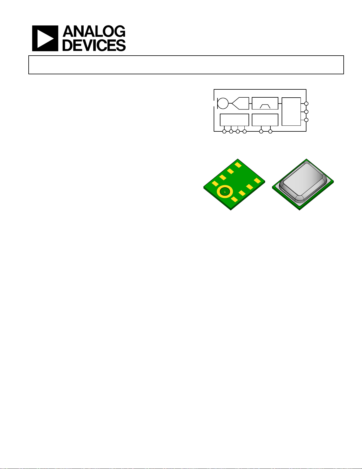
FUNCTIONAL BLOCK DIAGRAM
ADMP441
GND
FILTER
HARDWARE
CONTROL
CHIPEN
Figure 1.
I2S
SERIAL
PORT
L/R
SCK
SD
WS
09568-001
09568-015
ADC
POWER
MANAGEMENT
DD
V
GND
GND
BOTTOM TOP
Figure 2. Isometric Views of ADMP441 Microphone Package
GENERAL DESCRIPTION
The ADMP4411 is a high performance, low power, digital output,
omnidirectional MEMS microphone with a bottom port. The
complete ADMP441 solution consists of a MEMS sensor, signal
conditioning, an analog-to-digital converter, antialiasing filters,
power management, and an industry standard 24-bit IS interface. The IS interface allows the ADMP441 to connect directly
to digital processors, such as DSPs and microcontrollers, without the need for an audio codec in the system.
1
Protected by U.S. Patents 7,449,356; 7,825,484; 7,885,423; and 7,961,897. Other patents are pending.
The ADMP441 has a high SNR and high sensitivity, making it
an excellent choice for far field applications. The ADMP441 has
a flat wideband frequency response, resulting in natural sound
with high intelligibility. A built-in particle filter provides high
reliability.
The ADMP441 is available in a thin 4.72 mm × 3.76 mm ×
1 mm surface-mount package. It is reflow solder compatible
with no sensitivity degradation. The ADMP441 is halide free.
Rev. A
Information furnished by Analog Devices is believed to be accurate and reliable. However, no
responsibility is assumed by Anal og Devices for its use, nor for any infringements of patents or ot her
rights of third parties that may result from its use. Specifications subject to change without notice. No
license is granted by implication or otherwise under any patent or patent rights of Analog Devices.
Trademarks and registered trademarks are the property of their respective owners.
One Technology Way, P.O. Box 9106, Norwood, MA 02062-9106, U.S.A.
Tel: 781.329.4700 www.analog.com
Fax: 781.461.3113 ©2011–2012 Analog Devices, Inc. All rights reserved.
Page 2

ADMP441 Data Sheet
TABLE OF CONTENTS
Features.............................................................................................. 1
Applications....................................................................................... 1
Functional Block Diagram .............................................................. 1
General Description ......................................................................... 1
Revision History ............................................................................... 2
Specifications..................................................................................... 3
IS Digital Input/Output.............................................................. 4
Timing Diagram........................................................................... 4
Absolute Maximum Ratings............................................................ 5
ESD Caution.................................................................................. 5
Pin Configuration and Function Descriptions............................. 6
Typical Performance Characteristics ............................................. 7
Theory of Operation ........................................................................ 8
REVISION HISTORY
1/12—Rev. 0 to Rev. A
Changes to Circuit Note Title ....................................................... 11
Updated Outline Dimensions....................................................... 13
Deleted Figure 18............................................................................ 13
10/11—Revision 0: Initial Version
Understanding Sensitivity............................................................8
Power Management ......................................................................8
Startup.............................................................................................8
IS Data Interface ..........................................................................8
Digital Filter Characteristics..................................................... 10
Applications Information.............................................................. 11
Power Supply Decoupling......................................................... 11
Handling Instructions................................................................ 11
Supporting Documentation...................................................... 11
Layout and Design Recommendations........................................ 12
Outline Dimensions....................................................................... 13
Ordering Guide .......................................................................... 13
Rev. A | Page 2 of 16
Page 3

Data Sheet ADMP441
SPECIFICATIONS
TA = 25°C, VDD = 2.4 V, SCK = 3.072 MHz, SPL = 104 dB (3.16 Pa rms), unless otherwise noted. All minimum and maximum
specifications are guaranteed. Typical specifications are not guaranteed.
Table 1.
Parameter Symbol Test Conditions/Comments Min Typ Max Unit
PERFORMANCE
Directionality Omni
Sensitivity at 94 dB SPL1 1 kHz, 104 dB SPL −29 −26 −23 dBFS
Signal-to-Noise Ratio SNR 20 kHz bandwidth, A-weighted 61 dBA
Equivalent Input Noise EIN 20 kHz bandwidth, A-weighted 33 dBA SPL
Dynamic Range Derived from EIN and maximum acoustic input 87 dB
Frequency Response2 Low frequency –3 dB point 60 Hz
High frequency –3 dB point 15 kHz
Deviation limits from flat response within pass band −3/+2 dB
Total Harmonic Distortion THD 104 dB SPL 3 %
Power Supply Rejection PSR 217 Hz, 100 mV p-p square wave superimposed on VDD −75 dBFS
Maximum Acoustic Input Peak 120 dB SPL
Noise Floor 20 Hz to 20 kHz, A-weighted, rms −87 dBFS
POWER SUPPLY
Supply Voltage VDD 1.8 3.3 V
Supply Current IDD
VDD = 1.8 V
Normal Mode 1.4 1.6 mA
Standby 0.8 mA
Power-Down 2 µA
VDD = 3.3 V
Normal Mode 2.2 2.5 mA
Standby 0.8 mA
Power-Down 4.5 µA
DIGITAL FILTER
Group Delay 17.25/fS sec
f
f
Pass-Band Ripple ±0.04 dB
Stop-Band Attenuation 60 dB
Pass Band 0.423 × fS 20.3 kHz
1
The peak-to-peak amplitude is relative to peak-to-peak amplitude of 224 − 1. The stimulus is a 104 dB SPL sinusoid having rms amplitude of 3.1623 Pa. Sensitivity is
relative to 1 Pa.
2
See Figure 6 and Figure 8.
= 48 kHz 359 µs
S
= 16 kHz 1078 µs
S
Rev. A | Page 3 of 16
Page 4
ADMP441 Data Sheet
K
I²S DIGITAL INPUT/OUTPUT
–40°C < TA < +85°C, 1.8 V < VDD < 3.3 V, unless otherwise noted.
Table 2.
Limit1
Parameter Symbol Test Conditions/Comments Min Max Unit
DIGITAL INPUT
Voltage Input Low (L/R, WS, SCK) VIL 0
Voltage Input High (L/R, WS, SCK) VIH 0.7 × VDD VDD V
SD DIGITAL OUTPUT
Voltage Output Low VOL V
Voltage Output Low VOL V
Voltage Output High VOH V
Voltage Output High VOH V
Voltage Output Low VOL V
Voltage Output Low VOL V
Voltage Output High VOH V
Voltage Output High VOH V
1
Limits based on characterization results; not production tested.
= 1.8 V, I
DD
= 1.8 V, I
DD
= 1.8 V, I
DD
= 1.8 V, I
DD
= 3.3 V, I
DD
= 3.3 V, I
DD
= 3.3 V, I
DD
= 3.3 V, I
DD
= 0.25 mA 0.1 × VDD V
SINK
= 0.7 mA 0.3 × VDD V
SINK
= 0.7 mA 0.7 × VDD V
SINK
= 0.25 mA 0.9 × VDD V
SINK
= 0.5 mA 0.1 × VDD V
SINK
= 1.7 mA 0.3 × VDD V
SINK
= 1.7 mA 0.7 × VDD V
SINK
= 0.5 mA 0.9 × VDD V
SINK
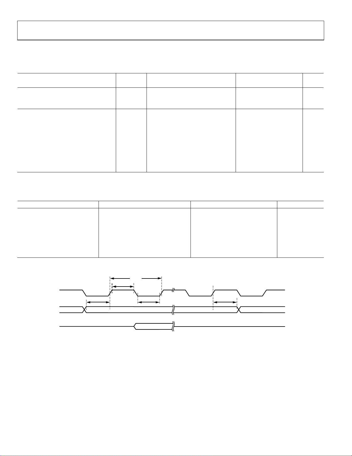
Table 3. Serial Data Port Timing Specifications
Parameter Description Min Max Unit
t
SCK high 50 ns
SCH
t
SCK low 50 ns
SCL
t
SCK period 312 ns
SCP
f
SCK
t
WS setup 0 ns
WSS
t
WS hold 20 ns
WSH
SCK frequency 0.5 3.2 MHz
fWS WS frequency 7.8 49.3 kHz
0.25 × VDD
V
TIMING DIAGRAM
SC
WS
SD
t
WSS
t
SCP
t
SCH
t
SCL
t
WSH
09568-103
Figure 3. Serial Data Port Timing
Rev. A | Page 4 of 16
Page 5
Data Sheet ADMP441
A
E
A
ABSOLUTE MAXIMUM RATINGS
Table 4.
Parameter Rating
Supply Voltage (VDD) −0.3 V to +3.6 V
Sound Pressure Level 160 dB
Mechanical Shock 10,000 g
Vibration
Per MIL-STD-883 Method
2007, Test Condition B
Operating Temperature Range −40°C to +85°C
Digital Pin Input Voltage
−0.3 V to V
+ 0.3 V or 3.6 V,
DD
whichever is less
Stresses above those listed under Absolute Maximum Ratings
may cause permanent damage to the device. This is a stress
rating only; functional operation of the device at these or any
other conditions above those indicated in the operational
section of this specification is not implied. Exposure to absolute
maximum rating conditions for extended periods may affect
device reliability.
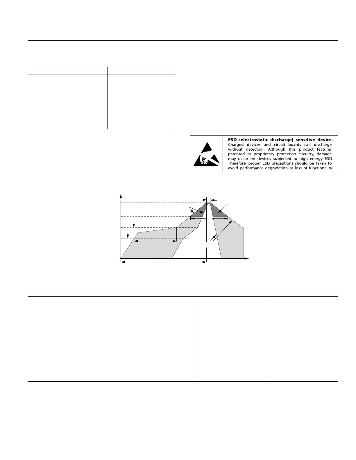
ESD CAUTION
LZON
CRITIC
TLTO T
P
t
L
09568-002
T
T
TURE
TEMPER
t
P
L
T
SMAX
T
SMIN
PREHEAT
t
25°C
t
S
RAMP-UP
TO PEAK
P
RAMP-DOWN
TIME
Figure 4. Recommended Soldering Profile Limits
Table 5. Recommended Soldering Profile Limits
Profile Feature Sn63/Pb37 Pb-Free
Average Ramp Rate (TL to TP) 1.25°C/sec max 1.25°C/sec max
Preheat
Minimum Temperature (T
Maximum Temperature (T
Time (T
Ramp-Up Rate (T
SMIN
to T
), tS 60 sec to 75 sec 60 sec to 75 sec
SMAX
to TL) 1.25°C/sec 1.25°C/sec
SMAX
) 100°C 100°C
SMIN
) 150°C 200°C
SMAX
Time Maintained Above Liquidous (tL) 45 sec to 75 sec ~50 sec
Liquidous Temperature (TL) 183°C 217°C
Peak Temperature (TP) 215°C +3°C/−3°C 260°C +0°C/−5°C
Time Within 5°C of Actual Peak Temperature (tP) 20 sec to 30 sec 20 sec to 30 sec
Ramp-Down Rate 3°C/sec max 3°C/sec max
Time 25°C (t
) to Peak Temperature 5 minute max 5 minute max
25°C
Rev. A | Page 5 of 16
Page 6

ADMP441 Data Sheet
A
PIN CONFIGURATION AND FUNCTION DESCRIPTIONS
DMP441
4L/R 6 GND
3WS 7 V
2SD 8 CHIPEN
1SCK 9 GND
Figure 5. Pin Configuration
5GND
BOTTOM VIEW
(Not to Scale)
DD
09568-003
Table 6. Pin Function Descriptions
Pin No. Mnemonic Type Description
1 SCK Input Serial Data Clock for I²S Interface.
2 SD Output
Serial Data Output for I²S Interface. This pin tristates when not actively driving the appropriate
output channel. The SD trace should have a 100 kΩ pull-down resistor to discharge the line during
the time that all microphones on the bus have tristated their outputs.
3 WS Input Serial Data-Word Select for I²S Interface.
4 L/R Input
Left/Right Channel Select. When set low, the microphone outputs its signal in the left channel of
the I²S frame; when set high, the microphone outputs its signal in the right channel.
5 GND Ground Ground. Connect to ground on the PCB.
6 GND Ground Ground. Connect to ground on the PCB.
7 VDD Power Power, 1.8 to 3.3 V. This pin should be decoupled to Pin 6 with a 0.1 F capacitor.
8 CHIPEN Input
Microphone Enable. When set low (ground), the microphone is disabled and put in power-down
mode. When set high (V
), the microphone is enabled.
DD
9 GND Ground Ground. Connect to ground on the PCB.
Rev. A | Page 6 of 16
Page 7

Data Sheet ADMP441
TYPICAL PERFORMANCE CHARACTERISTICS
10
8
6
4
2
0
–2
SENSITIVITY (dB)
–4
–6
–8
–10
50 100 10k
1k
FREQUENCY (Hz)
Figure 6. Frequency Response Mask
0
–10
–20
09568-009
10
0
AMPLITUDE (dB)
–10
–20
10 100 10k
FREQUENCY (Hz)
1k
09568-011
Figure 8. Typical Frequency Response (Measured)
–30
–40
PSR (dB)
–50
–60
–70
–80
100 10k
1k
FREQUENC Y (Hz)
09568-010
Figure 7. Typical Power Supply Rejection vs. Frequency
Rev. A | Page 7 of 16
Page 8

ADMP441 Data Sheet
THEORY OF OPERATION
The ADMP441 is a high performance, low power, digital
output, omnidirectional MEMS microphone with a bottom
port. The complete ADMP441 solution consists of a MEMS
sensor, signal conditioning, an analog-to-digital converter, antialiasing filters, power management, and an industry standard
24-bit IS interface.
The ADMP441 complies with the TIA-920 Te le co m mu ni ca t io ns
Telephone Terminal Equipment Transmission Requirements for
Wideband Digital Wireline Telephones standard.
UNDERSTANDING SENSITIVITY
The casual user of digital microphones may have difficulty
understanding the sensitivity specification. Unlike an analog
microphone (whose specification is easily confirmed with an
oscilloscope), the digital microphone output has no obvious
unit of measure.
The ADMP441 has a nominal sensitivity of −26 dBFS at 1 kHz
with an applied sound pressure level of 94 dB. The units are in
decibels referred to full scale. The ADMP441 default full-scale
peak output word is 2
−26 dBFS of that scale is (2
23
– 1 (integer representation), and
23
− 1) × 10
(−26/20)
= 420,426. A pure
acoustic tone at 1 kHz having a 1 Pa rms amplitude results in an
output digital signal whose peak amplitude is 420,426.
Although the industry uses a standard specification of 94 dB
SPL, the ADMP441 test method applies a 104 dB SPL signal.
The higher sound pressure level reduces noise and improves
repeatability. The ADMP441 has excellent gain linearity, and
the sensitivity test result at 94 dB is derived with very high
confidence from the test data.
POWER MANAGEMENT
The ADMP441 has three different power states: normal
operation, standby mode, and power-down mode.
Normal Operation
The microphone becomes operational 218 clock cycles (85 ms
with SCK at 3.072 MHz) after initial power-up. The CHIPEN
pin then controls the power modes. The part is in normal operation mode when SCK is active and the CHIPEN pin is high.
Standby Mode
The microphone enters standby mode when the serial data
clock SCK stops and CHIPEN is high. Normal operation
resumes 2
SCK restarts.
The ADMP441 should not be transitioned from standby to
power-down mode, or vice versa. Standby mode is only
intended to be entered from the normal operation state.
14
clock cycles (5 ms with SCK at 3.072 MHz) after
Power-Down Mode
The microphone enters power-down mode when CHIPEN is
low, regardless of the SCK operation. Normal mode operation
resumes 2
17
SCK clock cycles (43 ms with SCK at 3.072 MHz)
after CHIPEN returns high while SCK is active.
It always takes 2
17
clock cycles to restart the ADMP441 after VDD
is applied.
It is not recommended to supply active clocks (WS and SCK) to
the ADMP441 while there is no power supplied to V
. Doing
DD
this continuously turns on ESD protection diodes, which may
affect long-term reliability of the microphone.
STARTUP
The microphones have zero output for the first 218 SCK clock
cycles (85 ms with SCK at 3.072 MHz) following power-up.
I²S DATA INTERFACE
The slave serial data port’s format is IS, 24-bit, twos complement. There must be 64 SCK cycles in each WS stereo frame, or
32 SCK cycles per data-word. The L/R control pin determines
whether the ADMP441 outputs data in the left or right channel.
For a stereo application, the SD pins of the left and right
ADMP441 microphones should be tied together as shown in
Figure 9. The format of a stereo IS data stream is shown in
Figure 10. Figure 11 and Figure 12 show the formats of a mono
microphone data stream for left and right microphones,
respectively.
Data Output Mode
The output data pin (SD) is tristated when it is not actively
driving IS output data. SD immediately tristates after the LSB
is output so that another microphone can drive the common
data line.
The SD trace should have a pull-down resistor to discharge the
line during the time that all microphones on the bus have
tristated their outputs. A 100 k resistor is sufficient for this, as
shown in Figure 9.
Data-Word Length
The output data-word length is 24 bits per channel. The
ADMP441 must always have 64 clock cycles for every stereo
data-word (f
Data-Word Format
The default data format is IS (twos complement), MSB-first. In
this format, the MSB of each word is delayed by one SCK cycle
from the start of each half-frame.
= 64 × fWS).
SCK
Rev. A | Page 8 of 16
Page 9

Data Sheet ADMP441
V
S
S
S
FROM VOLTAGE
REGULATOR
(1.8V TO 3.3V)
0.1µF
DD
CHIPEN SCK
L/R SD
V
DD
LEFT
ADMP441
GND GND GND
WS
SYSTEM MASTER
(DSP, MICROCONTROLLER,
CODEC)
SCK
WS
SD
WS
100kΩ
Figure 9. System Block Diagram
0.1µF
V
DD
RIGHT
ADMP441
GND GND GND
V
DD
CHIPENSCK
L/RSD
09568-004
CK (64 ×
SD (24-BIT)
CK (64 ×
SD (24-BIT)
CK (64 ×
SD (24-BIT)
WS
WS
WS
1 2 3 4 24 25 26 32 33 34 35 36 56 57 58 64
f
)
S
MSB LSB
LEFT CHAN NEL
MSB LSB
RIGHT CHANNE LHIGH-Z HIGH-Z HIGH-Z
09568-005
Figure 10. Stereo Output I²S Format
1 2 3 4 24 25 26 32 33 34 3 5 36 56 57 58 64
f
)
S
MSB LSB
LEFT CHAN NELHIGH-Z
HIGH-Z
09568-006
Figure 11. Mono Output I²S Format Left Channel (L/R = 0)
1 2 3 4 24 25 26 32 33 34 3 5 36 56 57 58 64
f
)
S
MSB LSB
RIGHT CHANNE LHIGH-Z HIGH-Z
09568-007
Figure 12. Mono Output I²S Format Right Channel (L/R = 1)
Rev. A | Page 9 of 16
Page 10

ADMP441 Data Sheet
DIGITAL FILTER CHARACTERISTICS
The ADMP441 has an internal digital band-pass filter. A
high-pass filter eliminates unwanted low frequency signals.
A low-pass filter allows the user to scale the pass band with
the sampling frequency as well as perform required noise
reduction.
High Pass Filter
The ADMP441 incorporates a high-pass filter to remove unwanted
dc and very low frequency components. Tab le 7 shows the highpass characteristics for a nominal sampling rate of 48 kHz. The
cutoff frequency scales with changes in sampling rate.
Table 7. High-Pass Filter Characteristics
Frequency Attenuation
3.7 Hz –3.0 dB
10.4 Hz –0.5 dB
21.6 Hz –0.1 dB
This digital filter response is in addition to the natural highpass response of the ADMP441 MEMS acoustic transducer that
has a −3 dB cutoff of 60 Hz.
Low-Pass Filter
The analog-to-digital converter in the ADMP441 is a single-bit,
high order, sigma-delta (Σ-) running at a high oversampling
ratio. The noise shaping of the converter pushes the majority of
the noise well above the audio band and gives the microphone a
wide dynamic range. However, it does require a good quality
low-pass filter to eliminate the high frequency noise.
Figure 13 shows the response of this digital low-pass filter
included in the microphone. The pass band of the filter extends
to 0.423 × f
ripple. The high frequency cutoff of −6 dB occurs at 0.5 × f
and, in that band, has an unnoticeable 0.04 dB of
S
S
. A
48 kHz sampling rate results in a pass band of 20.3 kHz and a
half amplitude corner at 24 kHz; the stop-band attenuation of
the filter is greater than 60 dB. Note that these filter specifications scale with sampling frequency.
0
–10
–20
–30
–40
–50
–60
MAGNIT UDE (dB)
–70
–80
–90
–100
0 0.1 0.2 0.3 0.4 0. 5 0.6 0.7 0.8 0.9 1.0
NORMALI ZED FR EQUENCY (
Figure 13. Digital Low-Pass Filter Magnitude Response
f
)
S
09568-008
Rev. A | Page 10 of 16
Page 11

Data Sheet ADMP441
V
APPLICATIONS INFORMATION
POWER SUPPLY DECOUPLING
For best performance and to avoid potential parasitic artifacts,
placing a 0.1 µF ceramic type X7R or better capacitor between
Pin 7 (V
capacitor should be placed as close to Pin 7 as possible.
The connections to each side of the capacitor should be as short
as possible, and the trace should stay on a single layer with no
vias. For maximum effectiveness, locate the capacitor equidistant
from the power and ground pins or, when equidistant placement
is not possible, slightly closer to the power pin. Thermal connections to the ground planes should be made on the far side of the
capacitor, as shown in Figure 14.
) and ground is strongly recommended. The
DD
GND
DD
• Do not pick up the microphone with a vacuum tool that
makes contact with the bottom side of the microphone.
Do not pull air out of or blow air into the microphone port.
• Do not use excessive force to place the microphone on
the PCB.
Reflow Solder
For best results, the soldering profile should be in accordance
with the recommendations of the manufacturer of the solder
paste used to attach the MEMS microphone to the PCB. It is
recommended that the solder reflow profile does not exceed the
limit conditions specified in Figure 4 and Ta ble 5.
Board Wash
When washing the PCB, ensure that water does not make
contact with the microphone port. Blow-off procedures and
ultrasonic cleaning must not be used.
CAPACITOR
TO V
DD
TO GND
Figure 14. Recommended Power Supply Bypass Capacitor Layout
09568-012
HANDLING INSTRUCTIONS
Pick-and-Place Equipment
The MEMS microphone can be handled using standard pickand-place and chip shooting equipment. Care should be taken
to avoid damage to the MEMS microphone structure as follows:
• Use a standard pickup tool to handle the microphone.
Because the microphone hole is on the bottom of the
package, the pickup tool can make contact with any part
of the lid surface.
• Use care during pick-and-place to ensure that no high
shock events above 10,000 g are experienced because such
events may cause damage to the microphone.
SUPPORTING DOCUMENTATION
Evaluation Board User Guide
UG-303, EVAL-ADMP441Z-FLEX: Bottom-Port I2S Output
MEMS Microphone Evaluation Board
Circuit Note
CN-0208, High Performance Digital MEMS Microphone's Simple
Interface to SigmaDSP Audio Processor with I
Application Notes
AN-1112 Application Note, Microphone Specifications and
Ter m s E xp l aine d
AN-1003 Application Note, Recommendations for Mounting and
Connecting Analog Devices, Inc., Bottom-Ported MEMS
Microphones
AN-1068 Application Note, Reflow Soldering of the MEMS
Microphone
AN-1124 Application Note, Recommendations for Sealing
Analog Devices, Inc., Bottom-Port MEMS Microphones from
Dust and Liquid Ingress
For additional information, visit www.analog.com/mic.
2
S Output
Rev. A | Page 11 of 16
Page 12

ADMP441 Data Sheet
LAYOUT AND DESIGN RECOMMENDATIONS
1.05
(6×)
0.25 DIA.
(THRU HOLE )
2.66 (4×)
0.96
1.33 (2×)
1.56
0.40 × 0.60
(8×)
DIMENSIONS SHOWN IN MILL IMET ERS
3.16
09568-013
Figure 15. Recommended Printed Circuit Board Land Pattern
(Dimensions shown in millimeters)
1.05
(6×)
0.20
2.66 (4×)
0.350 × 0.550
(8×)
4.72
DIMENSIO NS SHOWN IN MILL IMETE RS
1.05
1.07
1.6
1.33 (2×)
3.76
09568-014
Figure 16. Recommended Printed Circuit Board Solder Paste Mask Pattern
(Dimensions shown in millimeters)
Rev. A | Page 12 of 16
Page 13

Data Sheet ADMP441
OUTLINE DIMENSIONS
4.82
4.10 REF
4.72
4.62
N
1
I
P
3.14
REF
C
E
E
R
E
N
R
E
F
E
R
R
O
N
C
3.86
3.76
3.66
0
4
.
0
N
I
P
(
2.66 BSC
×
S
0.30
0
6
.
0
)
8
-
1
1.05 BSC
1
5
96
1.07
1.56 DIA.
4
0.96 DIA.
0.275
0.250 DIA.
0.225
1.33 BSC
1.05
0.98
0.88
TOP VIEW
SIDE VIEW
0.73 REF
0.24 REF
BOTTOM VIEW
12-19-2011-B
Figure 17. 9-Terminal Chip Array Small Outline No Lead Cavity [LGA_CAV]
4.72 mm × 3 .76 mm × 1 mm Body
(CE-9-1)
(Dimensions shown in millimeters)
ORDERING GUIDE
Model1 Temperature Range Package Description Package Option2 Ordering Quantity
ADMP441ACEZ-RL −40°C to +85°C 9-Terminal LGA_CAV, 13” Tape and Reel CE-9-1 4,500
ADMP441ACEZ-RL7 −40°C to +85°C 9-Terminal LGA_CAV, 7” Tape and Reel CE-9-1 1,000
EVAL-ADMP441Z Evaluation Board
EVAL-ADMP441Z-FLEX Flex Evaluation Board
1
Z = RoHS Compliant Part.
2
This package option is halide-free.
Rev. A | Page 13 of 16
Page 14

ADMP441 Data Sheet
NOTES
Rev. A | Page 14 of 16
Page 15

Data Sheet ADMP441
NOTES
Rev. A | Page 15 of 16
Page 16

ADMP441 Data Sheet
NOTES
©2011–2012 Analog Devices, Inc. All rights reserved. Trademarks and
registered trademarks are the property of their respective owners.
D09568-0-1/12(A)
Rev. A | Page 16 of 16
 Loading...