

Page 1
Single-Chip, DSP-Based
a
FEATURES
26 MIPS Fixed-Point DSP Core
Single Cycle Instruction Execution (38.5 ns)
ADSP-21xx Family Code Compatible
16-Bit Arithmetic and Logic Unit (ALU)
Single Cycle 16-Bit 16-Bit Multiply and Accumulate
Into 40-Bit Accumulator (MAC)
32-Bit Shifter (Logical and Arithmetic)
Multifunction Instructions
Single Cycle Context Switch
Zero Overhead Looping
Conditional Instruction Execution
Two Independent Data Address Generators
Memory Configuration
2K 24-Bit Internal Program Memory RAM
2K 24-Bit Internal Program Memory ROM
1K 16-Bit Internal Data Memory RAM
14-Bit Address Bus and 24-Bit Data Bus for External
Memory Expansion
High Resolution Multichannel ADC
12-Bit Pipeline Flash Analog-to-Digital Converter
Eight Dedicated Analog Inputs
Simultaneous Sampling Capability
All Eight Inputs Converted in <2 s
4.0 V p-p Input Voltage Range
PWM Synchronized or External Convert Start
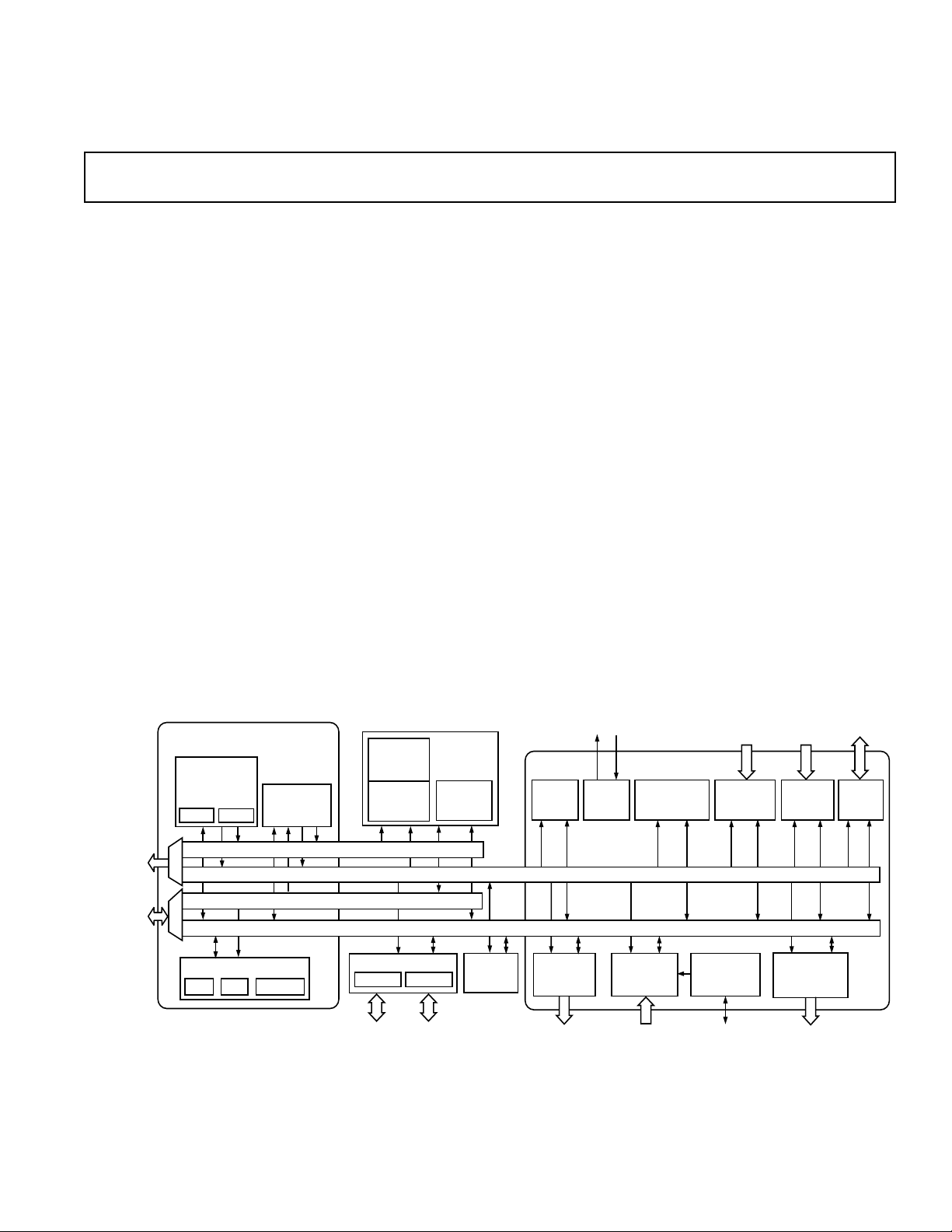
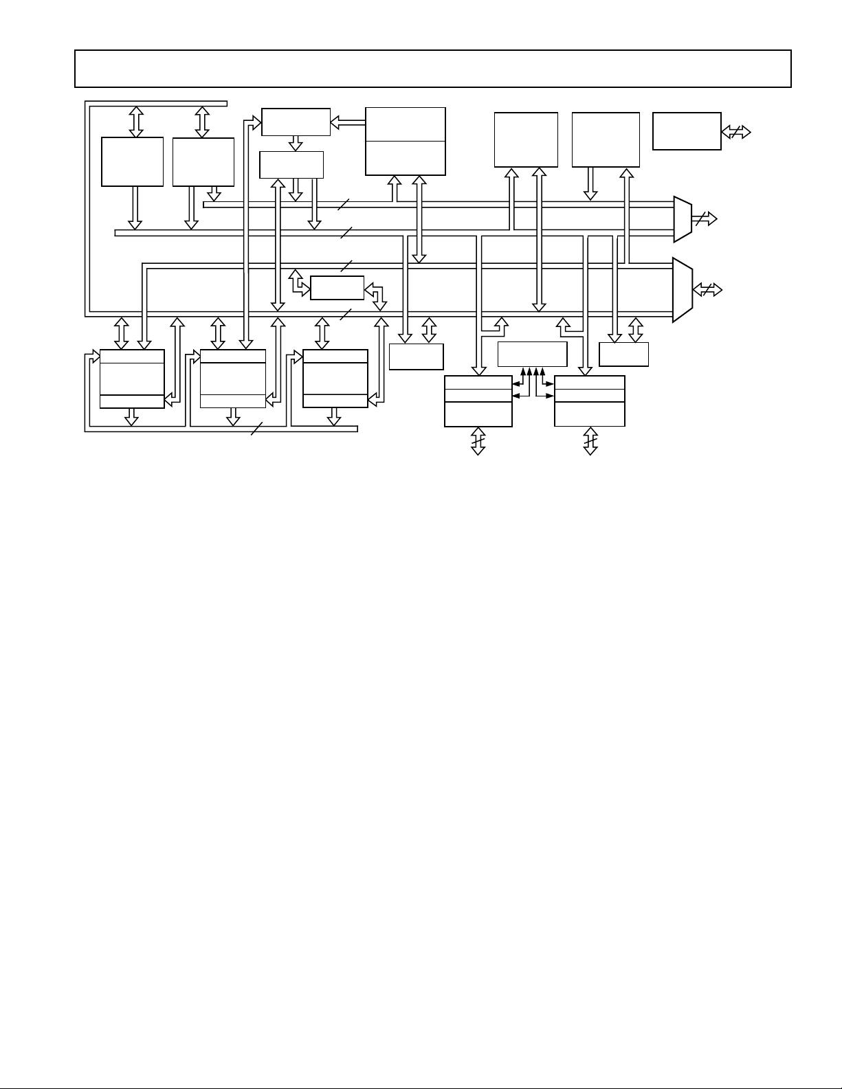
FUNCTIONAL BLOCK DIAGRAM
High Performance Motor Controller
ADMC401
Internal or External Voltage Reference
Out-of-Range Detection
Voltage Reference
Internal 2.0 V 2.0% Voltage Reference
Three-Phase 16-Bit PWM Generation Unit
Programmable Switching Frequency, Dead Time and
Minimum Pulsewidth
Edge Resolution of 38.5 ns
One or Two Updates per Switching Period
Hardware Polarity Control
Individual Enable/Disable of Each Output
High Frequency Chopping Mode
Dedicated Shutdown Pin (PWMTRIP)
Additional Shutdown Pins in I/O System
High Output Sink and Source Capability (10 mA)
Incremental Encoder Interface Unit
Quadrature Rates to 17.3 MHz
Programmable Filtering of Encoder Inputs
Alternative Frequency and Direction Mode
Two Registration Inputs to Latch Count Value
Optional Hardware Reset of Counter
Single North Marker Mode
Count Error Monitor Function
Dedicated 16-Bit Loop Timer (Periodic Interrupts)
Companion Encoder Event (1/T) Timer
(Continued on Page 14)
EXTERNAL
ADDRESS
BUS
EXTERNAL
DATA
BUS
26 MIPS DSP CORE
DATA
ADDRESS
GENERATORS
DAG 1
DAG 2
PROGRAM MEMORY ADDRESS
DATA MEMORY ADDRESS
PROGRAM MEMORY DATA
DATA MEMORY DATA
ARITHMETIC UNITS
ALU
MAC
PROGRAM
SEQUENCER
SHIFTER
PM
ROM
2K 24
PM
RAM
2K 24
SERIAL PORTS
SPORT 0
SPORT 1
MEMORY
DM
RAM
1K 16
REV. B
Information furnished by Analog Devices is believed to be accurate and
reliable. However, no responsibility is assumed by Analog Devices for its
use, nor for any infringements of patents or other rights of third parties
which may result from its use. No license is granted by implication or
otherwise under any patent or patent rights of Analog Devices.
MOTOR CONTROL
PERIPHERALS
WATCH-
TIMER
INTERVAL
TIMER
2 CHANNEL
AUXILIARY
One Technology Way, P.O. Box 9106, Norwood, MA 02062-9106, U.S.A.
Tel: 781/329-4700 World Wide Web Site: http://www.analog.com
Fax: 781/326-8703 © Analog Devices, Inc., 2000
DOG
PWM
POWER-
ON
RESET
INTERRUPT
CONTROLLER
8 CHANNEL
12-BIT ADC
ENCODER
INTERFACE
PRECISION
VOLTAGE
REFERENCE
EVENT
CAPTURE
UNIT
16-BIT
PWM
GENERATION
DIGITAL
I/O
UNIT
Page 2

ADMC401–SPECIFICATIONS
(VDD = AVDD = 5 V 5%, GND = AGND = 0 V, T
RECOMMENDED OPERATING CONDITIONS
CLKIN = 13 MHz, unless otherwise noted)
B Grade
Parameter Min Max Unit
V
AV
T
DD
AMB
Digital Supply Voltage 4.75 5.25 V
Analog Supply Voltage 4.75 5.25 V
DD
Ambient Operating Temperature –40 +85 °C
ELECTRICAL CHARACTERISTICS
Parameter Test Conditions Min Max Unit
V
IH
V
IL
V
OH
V
OL
V
OH
V
OL
I
IH
I
IH
I
IH
I
IL
I
IL
I
IL
I
OZH
I
OZL
I
DD
I
DD
I
DD
C
I
C
O
NOTES
1
Bidirectional pins: D0–D23, RFS0, RFS1, TFS0, TFS1, SCLK0 and SCLK1, PIO0–PIO11.
2
Input only pins: PWMTRIP, PWMPOL, PWMSR, RESET, EIA, EIB, EIZ, EIS, ETU0, ETU1, DR1A, DR1B, DR0, CLKIN, CONVST, MMAP, BMODE, BR
and PWD.
3
Programmable I/O Pins (PIO0–PIO11).
4
Output pins: PWMSYNC, AUX0, AUX1, CLKOUT, DT0, DT1, BG, BGH, PMS, DMS, BMS, RD, WR, PWDACK and A0–A13.
5
Output pins: AH, AL, BH, BL, CH and CL.
6
Although specified for TTL outputs, all ADMC401 outputs are CMOS-compatible and will drive to VDD–0.3 V and GND+0.3 V assuming no dc loads.
7
Input only pins RESET, EIA, EIB, EIZ, EIS, ETU0, ETU1, DR1A, DR1B, DR0, CLKIN, CONVST, MMAP, BMODE, BR and PWD.
8
Input pins with internal pull-down PIO0–PIO11 and PWMTRIP.
9
Input pins with internal pull-up, PWMPOL and PWMSR.
10
Three-statable pins: A0–A13, D0–D23, PMS, DMS, BMS, RD, WR, DT0, DT1, RFS0, RFS1, TFS0, TFS1, SCLK0, SCLK1.
11
Idle refers execution of the IDLE instruction. Deasserted pins are driven to VDD or GND. Current reflects device operation with CLKOUT disabled.
12
Current reflects device operating with no output loads.
13
Guaranteed but not tested.
14
Output Pin Capacitance is the capacitive load for any three-state output pin.
Specifications subject to change without notice.
HI-Level Input Voltage
LO-Level Input Voltage
HI-Level Output Voltage
LO-Level Output Voltage
HI-Level Output Voltage
LO-Level Output Voltage
HI-Level Input Current
HI-Level Input Current
HI-Level Input Current
LO-Level Input Current
LO-Level Input Current
LO-Level Input Current
HI-Level Three-State Leakage Current
LO-Level Three-State Leakage Current
Digital Supply Current (Idle)
Digital Supply Current (Dynamic)
Analog Supply Current @ AVDD = max 60 mA
Input Pin Capacitance
Output Pin Capacitance
1, 2, 3
1, 2, 3
1, 3, 4, 5, 6
1, 3, 4, 5, 6
5
5
7
8
9
7
8
9
13
13, 14
@ VDD = max 2.0 V
@ VDD = min 0.8 V
@ VDD = min, IOH = –1.0 mA 2.4 V
@ V
= min, IOH = –0.1 mA VDD – 0.3 V
DD
@ VDD = min, IOL = 2.0 mA 0.4 V
@ VDD = min, IOH = –10.0 mA 2.4 V
@ VDD = min, IOL = 10.0 mA 1.2 V
@ VDD = max, VIN = VDD max 10 µA
@ VDD = max, VIN = V
@ VDD = max, VIN = V
max 100 µA
DD
max 10 µA
DD
@ VDD = max, VIN = 0 V 10 µA
@ VDD = max, VIN = 0 V 10 µA
10
10
11
12
@ VDD = max, VIN = 0 V 100 µA
@ VDD = max, VIN = V
max 10 µA
DD
@ VDD = max, VIN = 0 V 10 µA
@ VDD = max 40 mA
@ VDD = max 110 mA
VIN = 2.5 V, fIN = 1 MHz, 8 pF
= +25°C
T
AMB
VIN = 2.5 V, fIN = 1 MHz, 8 pF
T
= +25°C
AMB
= –40C to +85C,
AMB
–2–
REV. B
Page 3

ADMC401
ANALOG-TO-DIGITAL CONVERTER
(VDD = AVDD = 5 V 5%, GND = AGND = 0 V, T
VIN0 to VIN7 = 4.0 V p-p, V
= 2.0 V, unless otherwise noted)
REF
= –40C to +85C, CLKIN = 13 MHz,
AMB
Parameter Test Conditions Min Typ Max Unit
AC SPECIFICATIONS
SNR Signal to Noise Ratio fIN = 1.0 kHz 68 70 dB
SNRD Signal to Noise and Distortion f
THD Total Harmonic Distortion f
CTLK Channel-Channel Crosstalk f
= 1.0 kHz 66 69 dB
IN
= 1.0 kHz –76 –70 dB
IN
= 1.0 kHz –89 –72 dB
IN
CMRR Common-Mode Rejection Ratio –90 –72 dB
PSRR Power Supply Rejection Ratio 0.025 0.1 % FSR
ACCURACY
INL Integral Nonlinearity ± 0.6 ± 1.5 LSB
DNL Differential Nonlinearity ± 0.5 ± 1.0 LSB
No Missing Codes 12 Bits Guaranteed
Zero Error 0.1 0.25 % FSR
Gain Error
1
0.4 1.0 % FSR
TEMPERATURE DRIFT
Zero Error 0.025 % FSR
Gain Error
1
0.025 % FSR
INPUT VOLTAGE
V
IN
C
IN
Voltage Span 4.0 V p-p
Input Capacitance
2
10 pF
CONVERSION TIME
t
CONV
NOTES
1
Excludes Internal Voltage Reference Error.
2
Analog Input Pins VIN0 to VIN7.
Typical values are neither tested nor guaranteed.
Specifications subject to change without notice.
Total Conversion Time All 8 Channels 1.88 µs
VOLTAGE REFERENCE
(VDD = AVDD = 5 V 5%, GND = AGND = 0 V, T
4.0 V p-p, V
= 2.0 V, unless otherwise noted)
REF
= –40C to +85C, CLKIN = 13 MHz, VIN0 to VIN7 =
AMB
Parameter Test Conditions Min Typ Max Unit
V
REF
Output Voltage Reference SENSE = REFCOM 1.96 2.0 2.04 V
Output Voltage Tolerance
1
SENSE = REFCOM 6 mV
Output Current 1.0 mA
Load Regulation 1.0 mA Load Current 0.3 1.5 mV
Power Supply Rejection Ratio 0.1 1.5 mV
Reference Input Resistance 8 kΩ
NOTES
1
Relative tolerance due to temperature change, T
Specifications subject to change without notice.
POWER-ON RESET
(GND = AGND = 0 V, T
MIN
to T
.
MAX
= –40C to +85C, CLKIN = 13 MHz, unless otherwise noted)
AMB
Parameter Test Conditions Min Typ Max Unit
V
RST
V
HYST
Specifications subject to change without notice.
Reset Threshold Voltage 3.25 4.0 V
Hysteresis Voltage 75 mV
REV. B
–3–
Page 4

ADMC401
WARNING!
ESD SENSITIVE DEVICE
ABSOLUTE MAXIMUM RATINGS*
Supply Voltage . . . . . . . . . . . . . . . . . . . . . . . . . . –0.3 V to +7 V
Input Voltage . . . . . . . . . . . . . . . . . . . . . –0.3 V to V
Output Voltage Swing . . . . . . . . . . . . . . –0.3 V to V
Operating Temperature Range (Ambient) . . . . –40°C to +85°C
Storage Temperature Range . . . . . . . . . . . . . –65°C to +150°C
Lead Temperature (5 sec) . . . . . . . . . . . . . . . . . . . . . . +280°C
*Stresses above those listed under absolute maximum ratings may cause permanent
damage to the device. These are stresses only; functional operation of the device
at these or any other conditions above those indicated in the operational section of
this specification is not implied. Exposure to absolute maximum rating conditions
for extended periods may affect device reliability.
Temperature Instruction Package Package
Model Range Rate Description Option
ADMC401BST –40°C to +85°C 26 MHz 144-Lead Plastic Thin Quad Flatpack (LQFP) ST-144
ADMC401-ADVEVALKIT Development Tool Kit
ADMC401-PB Evaluation/Processor Board
CAUTION
ESD (electrostatic discharge) sensitive device. Electrostatic charges as high as 4000 V readily
accumulate on the human body and test equipment and can discharge without detection.
Although the ADMC401 features proprietary ESD protection circuitry, permanent damage may
occur on devices subjected to high-energy electrostatic discharges. Therefore, proper ESD
precautions are recommended to avoid performance degradation or loss of functionality.
+ 0.3 V
DD
+ 0.3 V
DD
ORDERING GUIDE
Timing Parameters
GENERAL NOTES
Use the exact timing information given. Do not attempt to
derive parameters from the addition or subtraction of others.
While addition or subtraction would yield meaningful results for
an individual device, the values given in this data sheet reflect
statistical variations and worst cases. Consequently, you cannot
meaningfully add up parameters to derive longer times.
TIMING NOTES
Switching characteristics specify how the processor changes its
signals. You have no control over this timing; it is dependent on
the internal design. Timing requirements apply to signals that
are controlled outside the processor, such as the data input for a
read operation.
Timing requirements guarantee that the processor operates
correctly with another device. Switching characteristics tell you
what the device will do under a given circumstance. Also, use
the switching characteristics to ensure any timing requirement
of a device connected to the processor (such as memory) is
satisfied.
MEMORY REQUIREMENTS
This chart links common memory device specification names
and ADMC401 timing parameters for your convenience.
Common
Parameter Memory Device
Name Function Specification Name
t
ASW
t
AW
t
WRA
t
DW
t
DH
t
RDD
t
AA
A0–A13, DMS, PMS Address Setup to
Setup before WR Low Write Start
A0–A13, DMS, PMS Address Setup to
before WR Deasserted Write End
A0–A13, DMS, PMS Address Hold Time
Hold after WR Deasserted
Data Setup before WR High Data Setup Time
Data Hold after WR High Data Hold Time
RD Low to Data Valid OE to Data Valid
A0–A13, DMS, PMS, Address Access Time
BMS to Data Valid
–4–
REV. B
Page 5
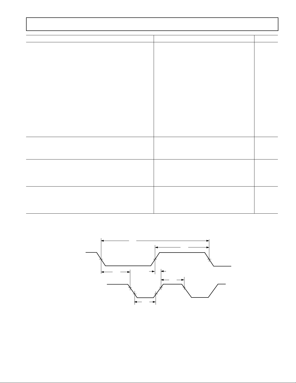
ADMC401
Parameter Min Max Unit
Clock Signals
t
is defined as 0.5t
CK
with a frequency equal to half the instruction rate; a 13 MHz
clock (which is equivalent to 76.9 ns) yields a 38.5 ns processor
cycle (equivalent to 26 MHz). t
0.5t
period should be substituted for all relevant timing
CKI
parameters to obtain specification value.
Example: t
= 0.5tCK – 10 ns = 0.5 (38.5 ns) – 10 ns = 9.25 ns.
CKH
Timing Requirements:
t
CKI
t
CKIL
t
CKIH
Switching Characteristics:
t
CKL
t
CKH
t
CKOH
Control Signals
Timing Requirement:
t
RSP
PWM Shutdown Signals
Timing Requirements:
t
PWMTPW
t
PIOPWM
ADC Signals
Timing Requirements:
t
CSI
t
CSE
NOTE
1
Applies after power-up sequence is complete. Internal phase lock loop requires no more than 2000 CLKIN cycles assuming stable CLKIN (not including crystal
oscillator start-up time).
The ADMC401 uses an input clock
CKI.
values within the range of
CK
CLKIN Period 76.9 150 ns
CLKIN Width Low 20 ns
CLKIN Width High 20 ns
CLKOUT Width Low 0.5t
CLKOUT Width High 0.5t
– 10 ns
CK
– 10 ns
CK
CLKIN High to CLKOUT High 0 20 ns
CK
CK
CK
CK
CK
1
ns
ns
ns
ns
ns
RESET Width Low 5t
PWMTRIP Width Low t
PIO Width Low 2t
Internal Convert Start Width High 2t
External Convert Start Width High 2t
REV. B
CLKIN
CLKOUT
t
t
CKI
CKIL
t
CKL
Figure 1. Clock Signals
–5–
t
CKOH
t
CKIH
t
CKH
Page 6
ADMC401
Parameter Min Max Unit
Interrupts and Flags
Timing Requirements:
t
t
IFS
IFH
IRQx or FI Setup before CLKOUT Low
IRQx or FI Hold after CLKOUT High
Switching Characteristics:
t
FOH
t
FOD
NOTES
1
If IRQx and FI inputs meet t
the following cycle. (Refer to “Interrupt Controller Operation” in the Program Control chapter of the ADSP-2100 Family User’s Manual, Third Edition for further
information on interrupt servicing.)
2
Edge-sensitive interrupts require pulsewidths greater than 10 ns; level-sensitive interrupts must be held low until serviced.
3
IRQx = IRQ0 and IRQ1.
4
Flag Output = FL1 and FO.
Flag Output Hold after CLKOUT Low
Flag Output Delay from CLKOUT Low
and t
IFS
setup/hold requirements, they will be recognized during the current clock cycle; otherwise the signals will be recognized on
IFH
CLKOUT
FLAG
OUTPUTS
1, 2, 3
1, 2, 3
4
4
0.25tCK + 15 ns
0.25t
CK
ns
0.5tCK – 7 ns
0.5tCK + 5 ns
t
FOD
t
FOH
t
IFH
IRQx
FI
t
IFS
Figure 2. Interrupts and Flags
–6–
REV. B
Page 7
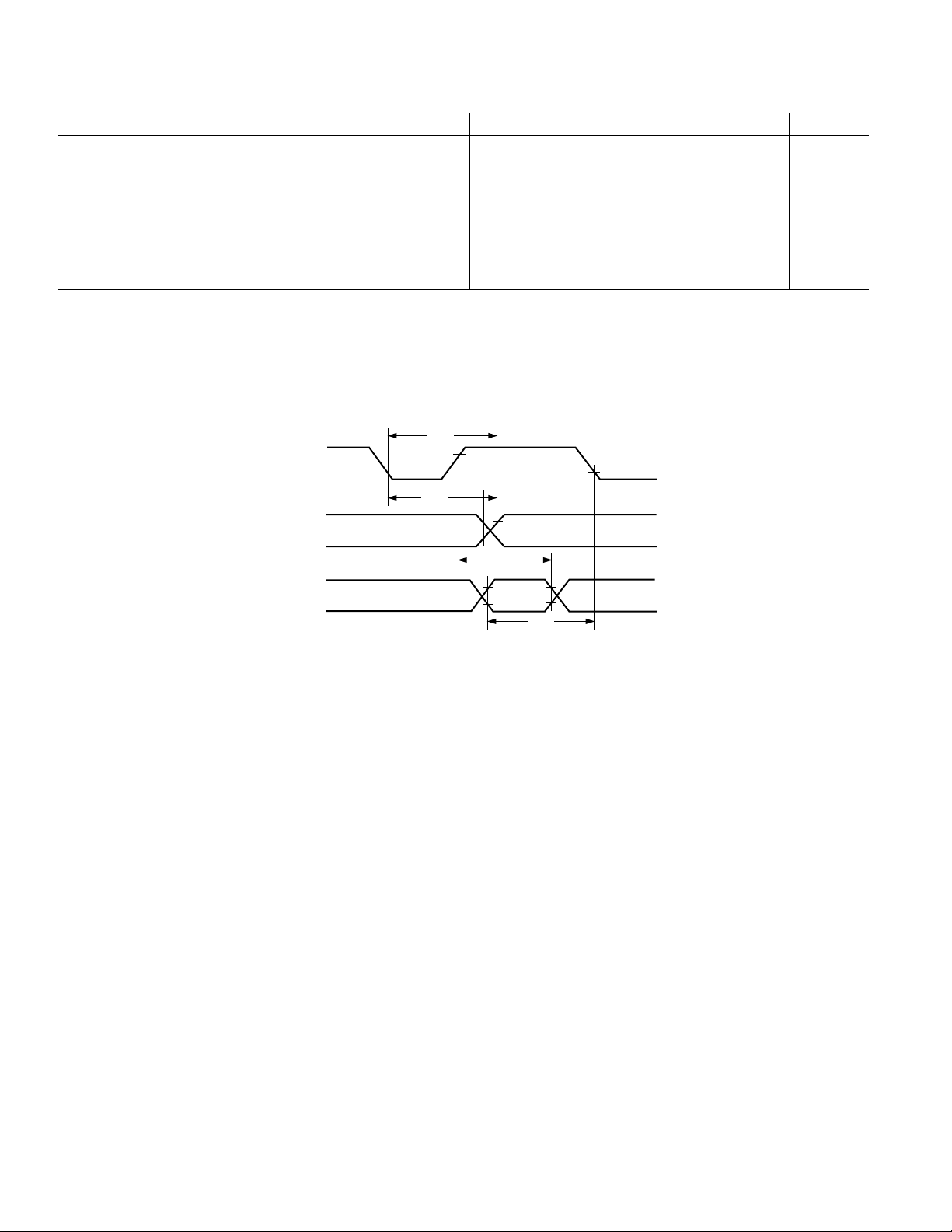
ADMC401
Parameter Min Max Unit
Bus Request/Grant
Timing Requirements:
t
BH
t
BS
BR Hold after CLKOUT High
BR Setup before CLKOUT Low
Switching Characteristics:
t
SD
CLKOUT High to DMS, PMS, BMS, 0.25tCK + 10 ns
RD, WR Disable
t
SDB
DMS, PMS, BMS, RD, WR
Disable to BG Low 0 ns
t
SE
BG High to DMS, PMS, BMS,
RD, WR Enable 0 ns
t
SEC
DMS, PMS, BMS, RD, WR
Enable to CLKOUT High 0.25t
t
SDBH
t
SEH
NOTES
1
BR is an asynchronous signal. If BR meets the setup/hold requirements, it will be recognized during the current clock cycle; otherwise the signal will be recognized
on the following cycle. Refer to the ADSP-2100 Family User’s Manual, Third Edition for BR/BG cycle relationships.
2
BGH is asserted when the bus is granted and the processor requires control of the bus to continue.
DMS, PMS, BMS, RD, WR
Disable to BGH Low
BGH High to DMS, PMS, BMS,
RD, WR Enable
2
2
1
1
0.25tCK +2 ns
0.25tCK + 17 ns
– 7 ns
CK
0ns
0ns
CLKOUT
BR
CLKOUT
PMS, DMS
BMS, RD
WR
BG
BGH
t
BH
t
BS
t
SD
t
SDB
t
SDBH
Figure 3. Bus Request–Bus Grant
t
SEC
t
SE
t
SEH
REV. B
–7–
Page 8
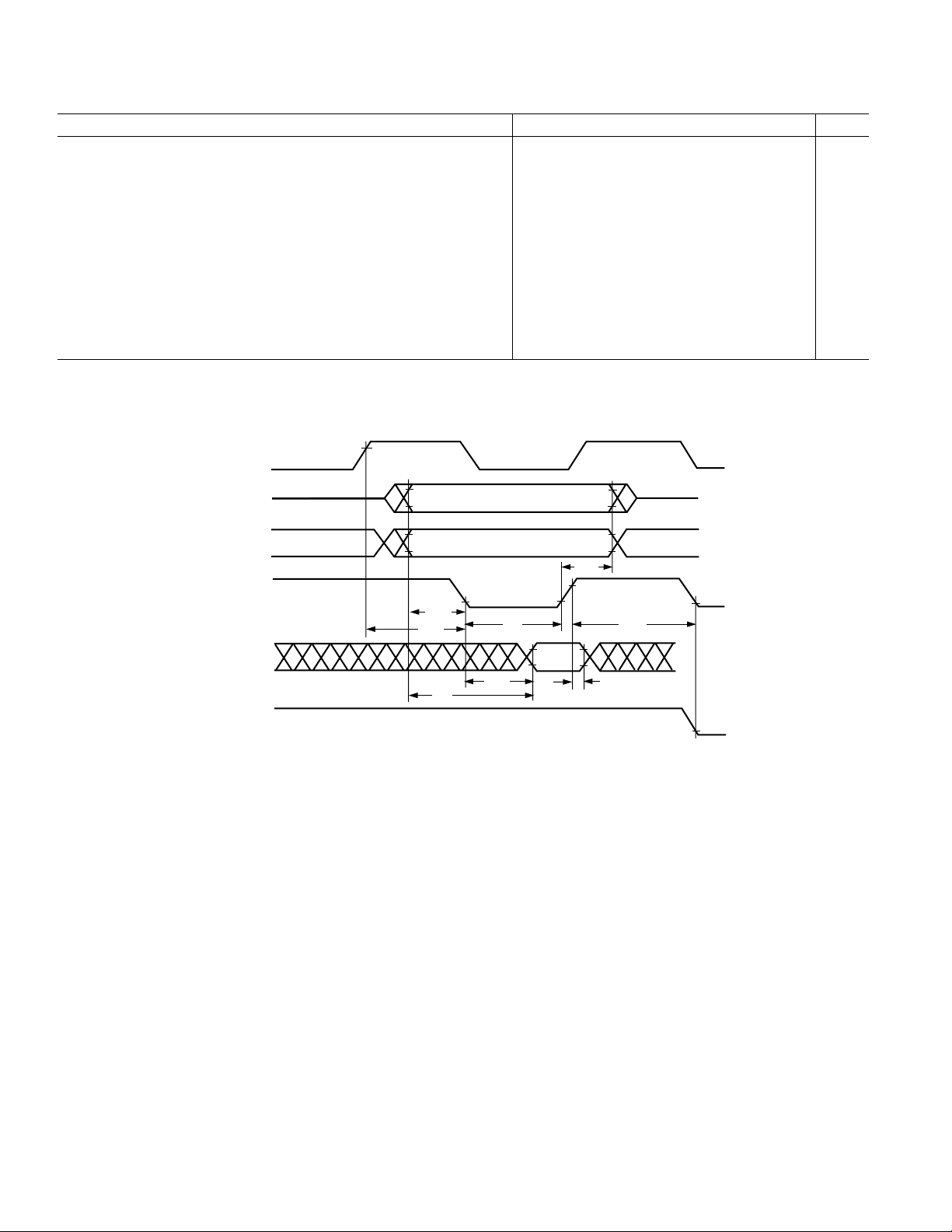
ADMC401
Parameter Min Max Unit
Memory Read
Timing Requirements:
t
RDD
t
AA
t
RDH
Switching Characteristics:
t
RP
t
CRD
t
ASR
t
RDA
t
RWR
w = wait states × tCK.
RD Low to Data Valid 0.5tCK – 11 + w ns
A0–A13, PMS, DMS, BMS to Data Valid 0.75tCK – 12 + w ns
Data Hold from RD High 0 ns
RD Pulsewidth 0.5tCK – 5 + w ns
CLKOUT High to RD Low 0.25tCK – 5 0.25tCK + 7 ns
A0–A13, PMS, DMS, BMS Setup before RD Low 0.25tCK – 6 ns
A0–A13, PMS, DMS, BMS Hold after RD Deasserted 0.25tCK – 3 ns
RD High to RD or WR Low 0.5t
CLKOUT
A0–A13
– 5 ns
CK
DMS, PMS
BMS
RD
WR
t
RDA
t
ASR
t
CRD
D
t
AA
t
RP
t
RDD
t
RWR
t
RDH
Figure 4. Memory Read
–8–
REV. B
Page 9
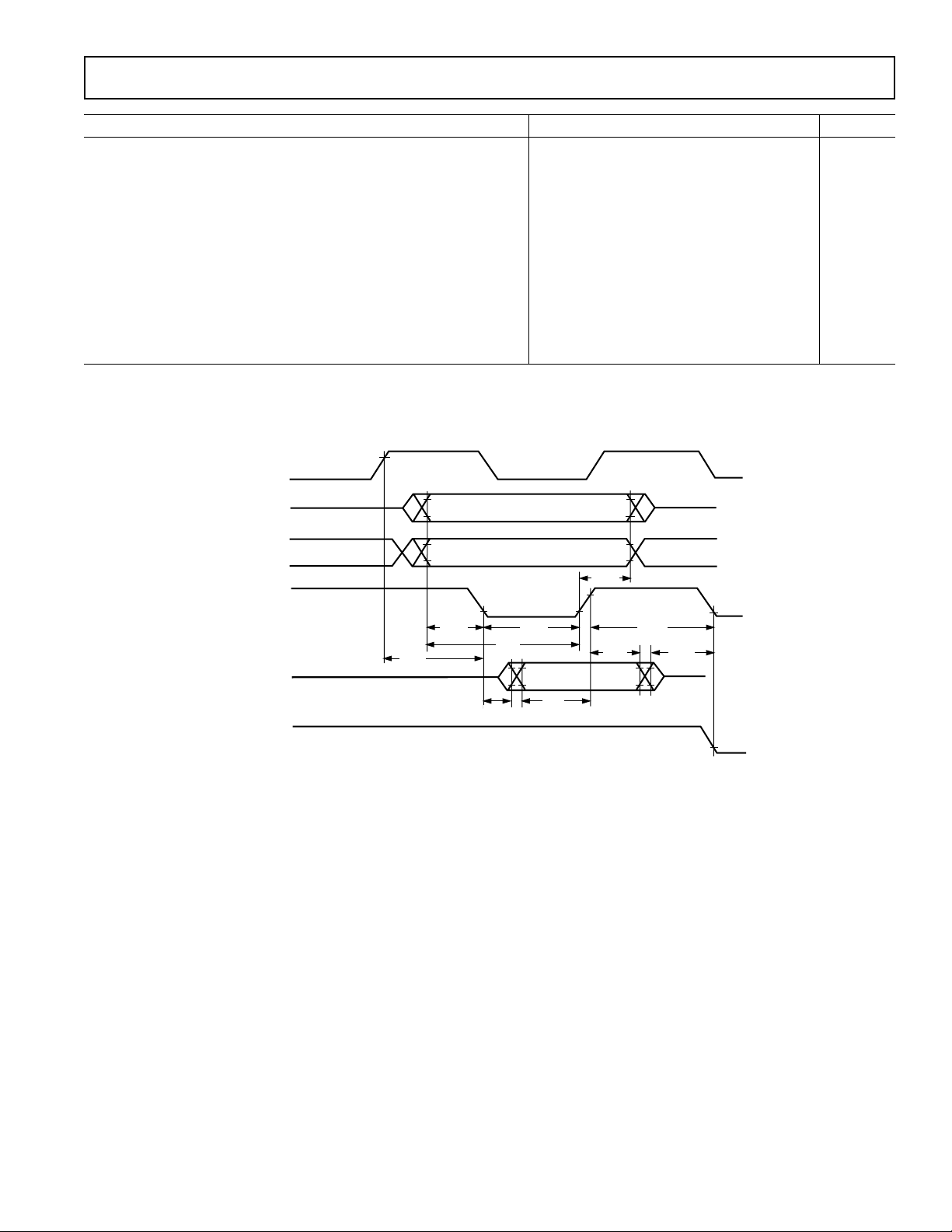
ADMC401
Parameter Min Max Unit
Memory Write
Switching Characteristics:
t
DW
t
DH
t
WP
t
WDE
t
ASW
t
DDR
t
CWR
t
AW
t
WRA
t
WWR
w = wait states × tCK.
Data Setup before WR High 0.5t
Data Hold after WR High 0.25t
– 7 + w ns
CK
– 2 ns
CK
WR Pulsewidth 0.5tCK – 5 + w ns
WR Low to Data Enabled 0 ns
A0–A13, DMS, PMS Setup before WR Low 0.25t
– 6 ns
CK
Data Disable before WR or RD Low 0.25tCK – 6 ns
CLKOUT High to WR Low 0.25t
A0–A13, DMS, PMS, Setup before WR Deasserted 0.75t
A0–A13, DMS, PMS Hold after WR Deasserted 0.25t
– 5 0.25tCK + 7 ns
CK
– 9 + w ns
CK
– 3 ns
CK
WR High to RD or WR Low 0.5tCK – 5 ns
CLKOUT
A0–A13
DMS, PMS
WR
RD
t
WRA
t
ASW
t
CWR
D
t
WP
t
AW
t
t
WDE
DW
t
WWR
t
DH
t
DDR
Figure 5. Memory Write
REV. B
–9–
Page 10
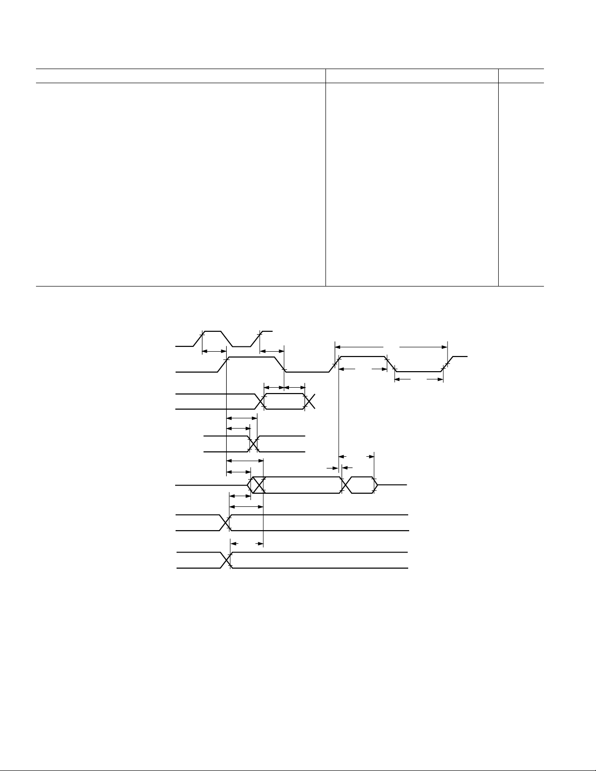
ADMC401
(
)
Parameter Min Max Unit
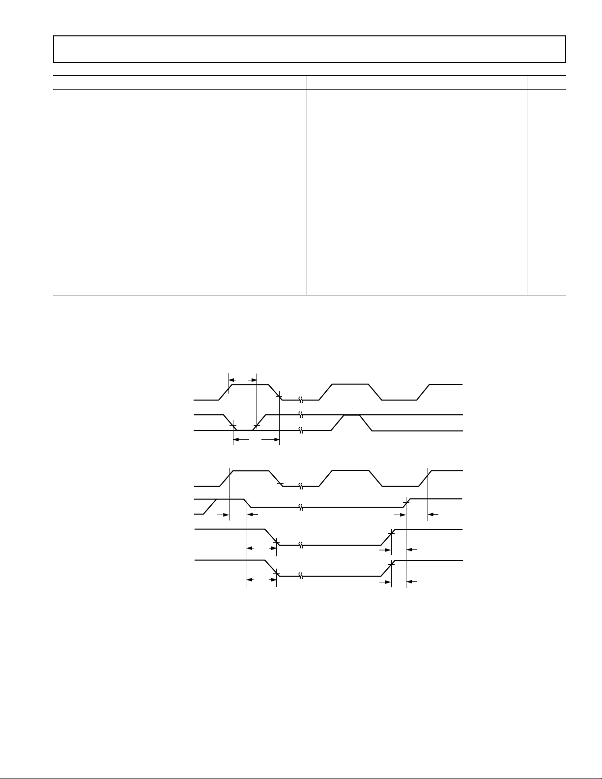
Serial Ports
Timing Requirements:
t
SCK
t
SCS
t
SCH
t
SCP
Switching Characteristics:
t
CC
t
SCDE
t
SCDV
t
RH
t
RD
t
SCDH
t
TDE
t
TDV
t
SCDD
t
RDV
SCLK Period 50 ns
DR/TFS/RFS Setup before SCLK Low 5 ns
DR/TFS/RFS Hold after SCLK Low 10 ns
SCLK
CLKOUT High to SCLK
Width 20 ns
IN
OUT
0.25t
CK
0.25t
+ 15 ns
CK
SCLK High to DT Enable 0 ns
SCLK High to DT Valid 20 ns
TFS/RFS
TFS/RFS
Hold after SCLK High 0 ns
OUT
Delay from SCLK High 20 ns
OUT
DT Hold after SCLK High 0 ns
TFS(Alt) to DT Enable 0 ns
TFS(Alt) to DT Valid 20 ns
SCLK High to DT Disable 20 ns
RFS (Multichannel, Frame Delay Zero) to DT Valid 20 ns
CLKOUT
SCLK
DR
RFS
TFS
RFS
OUT
TFS
OUT
TFS
alternate
frame mode
multichannel mode,
RFS
frame delay 0
MFD = 0
DT
t
CC
IN
IN
t
t
t
RD
t
RH
SCDV
SCDE
t
TDE
t
TDV
t
CC
t
SCS tSCS
t
t
SCDH
t
RDV
SCDD
t
SCK
t
SCP
t
SCP
Figure 6. Serial Ports
–10–
REV. B
Page 11
ADMC401
POWER DISSIPATION
To determine total power dissipation in a specific application,
the following equation should be applied for each output:
2
DD
× f
C × V
C = load capacitance, f = output switching frequency.
Example:
In an application where external data memory is used and no
other outputs are active, power dissipation is calculated as
follows:
Assumptions:
• External data memory is accessed every cycle with 50% of the
address pins switching.
• External data memory writes occur every other cycle with
50% of the data pins switching.
• Each address and data pin has a 10 pF total load at the pin.
• The application operates at V
Total Power Dissipation = P
= VDD × (IDD Digital + IDD Analog)
P
INT
(C × V
2
× f) is calculated for each output:
DD
# of
Pins C V
Address, DMS 8 × 10 pF × 52 V × 26 MHz = 52.00 mW
Data Output, WR 9 × 10 pF × 52 V × 13 MHz = 29.25 mW
RD 1 × 10 pF × 52 V × 13 MHz = 3.25 mW
CLKOUT 1 × 10 pF × 52 V × 26 MHz = 6.50 mW
Total power dissipation for this example is P
= 5.0 V and t
DD
+ (C × V
INT
2
f
DD
= 38.5 ns.
CK
2
× f)
DD
+ 91 mW.
INT
91.00 mW
INPUT
OUTPUT
0.0V
0.3V
1.5V
2.0V
1.5V
3.0V
Figure 7. Voltage Reference Levels for AC Measurements (Except Output Enable/Disable)
Output Enable Time
Output pins are considered to be enabled when that have made
a transition from a high-impedance state to when they start
driving. The output enable time (t
) is the interval from when
ENA
a reference signal reaches a high or low voltage level to when
the output has reached a specified high or low trip point, as
shown in the Output Enable/Disable diagram. If multiple pins
(such as the data bus) are enabled, the measurement value is
that of the first pin to start driving.
REFERENCE
SIGNAL
t
(MEASURED)
OUTPUT
(MEASURED)
V
OH
V
OL
MEASURED
t
DIS
V
(MEASURED) – 0.5V
OH
(MEASURED) +0.5V
V
OL
t
DECAY
OUTPUT STOPS
DRIVING
HIGH-IMPEDANCE STATE. TEST CONDITIONS CAUSE
THIS VOLTAGE LEVEL TO BE APPROXIMATELY 1.5V.
t
ENA
V
(MEASURED)
2.0V
1.0V
OUTPUT STARTS
DRIVING
V
(MEASURED)
OH
OL
Figure 8. Output Enable/Disable
TEST CONDITIONS
Output Disable Time
Output pins are considered to be disabled when they have
stopped driving and started a transition from the measured
output high or low voltage to a high impedance state. The output disable time (t
) is the difference of t
DIS
MEASURED
and t
DECAY
,
as shown in the Output Enable/Disable diagram. The time is the
interval from when a reference signal reaches a high or low
voltage level to when the output voltages have changed by 0.5 V
from the measured output high or low voltage. The decay time,
, is dependent on the capacitative load, CL, and the cur-
t
DECAY
rent load, i
, on the output pin. It can be approximated by the
L
following equation:
CV
× 05.
t
DECAY
L
=
I
L
from which
tt t
=−
DIS MEASURED DECAY
is calculated. If multiple pins (such as the data bus) are disabled, the measurement value is that of the last pin to stop
driving.
I
OL
OUTPUT
PIN
TO
50pF
I
OH
+1.5V
Figure 9. Equivalent Device Loading for AC Measurements (Including All Fixtures)
REV. B
–11–
Page 12

ADMC401
PIN FUNCTION DESCRIPTION
Pin Pin Pin Pin Pin Pin Pin Pin
No. Name No. Name No. Name No. Name
1 A9 37 RFS1/IRQ0/SROM 73 GND 109 CONVST
2 A8 38 TFS1/IRQ1 74 D10 110 GND
3 A7 39 SCLK1 75 D9 111 VDD
4 A6 40 DR0 76 D8 112 GND
5 VDD 41 DT0 77 D7 113 AVDD
6 A5 42 RFS0 78 D6 114 AVSS
7 A4 43 TFS0 79 D5 115 VIN7
8 A3 44 SCLK0 80 D4 116 V
9 GND 45 VDD 81 D3 117 VIN6
10 A2 46 GND 82 GND 118 REFCOM
11 A1 47 PWMTRIP 83 D2 119 VIN5
12 A0 48 PWMSYNC 84 D1 120 CAPT
13 PWD 49 CL 85 D0 121 VIN4
14 PWDACK 50 CH 86 P11 122 BSHAN
15 BR 51 VDD 87 P10 123 ASHAN
16 NC 52 GND 88 P9 124 VIN0
17 NC 53 BL 89 P8 125 CAPB
18 BMODE 54 BH 90 VDD 126 VIN1
19 MMAP 55 AL 91 GND 127 CML
20 VDD 56 AH 92 P7 128 VIN2
21 GND 57 BGH 93 P6 129 GAIN
22 PWMSR 58 D23 94 P5 130 VIN3
23 POR 59 D22 95 P4 131 SENSE
24 RESET 60 D21 96 P3 132 AVSS
25 GND 61 D20 97 P2 133 AVDD
26 GND 62 D19 98 GND 134 BMS
27 GND 63 GND 99 P1 135 PMS
28 PWMPOL 64 D18 100 P0 136 DMS
29 CLKIN 65 D17 101 AUX1 137 RD
30 XTAL 66 D16 102 AUX0 138 GND
31 CLKOUT 67 D15 103 ETU1 139 BG
32 VDD 68 D14 104 ETU0 140 WR
33 GND 69 D13 105 EIS 141 A13
34 DR1A/FI 70 D12 106 EIZ 142 A12
35 DRIB/FI 71 VDD 107 EIB 143 A11
36 DT1/FO 72 D11 108 EIA 144 A10
NC: These pins must be left unconnected
REF
–12–
REV. B
Page 13

PIN CONFIGURATION
A9A8A7
A6
VDD
A5A4A3
GND
A2A1A0
PWD
PWDACK
BRNCNC
BMODE
MMAP
VDD
GND
PWMSR
POR
RESET
GND
GND
GND
PWMPOL
CLKIN
XTAL
CLKOUT
VDD
GND
DR1A/F1
DR1B/FI
DT1/FO
P1
GNDP2P3P4P5P6P7
GND
VDDP8P9
P10
P11D0D1D2GNDD3D4D5D6D7D8D9D10
GND
EIA
EIB
EIZ
EIS
ETU0
ETU1
AUX0
AUX1
P0
D11
VDD
D12
D13
D14
D15
D16
D17
D18
GND
D19
D20
D21
D22
D23
BGH
AH
AL
BH
BL
GND
VDD
CH
CL
PWMSYNC
PWMTRIP
GND
VDD
SCLK0
TFS0
RFS0
DT0
DR0
SCLK1
TFS1/IRQ1
RFS1/IRQ0/SROM
CONVST
GND
VDD
GND
AVDD
AVSS
VIN7
V
REF
VIN6
REFCOM
VIN5
CAPT
VIN4
BSHAN
ASHAN
VIN0
CAPB
VIN1
CML
VIN2
GAIN
VIN3
SENSE
AVSS
AVDD
BMS
PMS
DMS
RD
GND
BG
WR
A13
A12
A11
A10
NC = NO CONNECT
PIN 1
IDENTIFIER
TOP VIEW
(Not to Scale)
ADMC401
1920212223242526272829303132333435
36
101112131415161718
123456789
9089888786858483828180797877767574
73
999897969594939291
108
107
106
105
104
103
102
101
100
72
71
70
69
68
67
66
65
64
63
62
61
60
59
58
57
56
55
54
53
52
51
50
49
48
47
46
45
44
43
42
41
40
39
38
37
109
110
111
112
113
114
115
116
117
118
119
120
121
122
123
124
125
126
127
128
129
130
131
132
133
134
135
136
137
138
139
140
141
142
143
144
ADMC401
REV. B
–13–
Page 14

ADMC401
(Continued from Page 1)
Programmable Digital I/O (PIO) Port
12-Pin Configurable Digital I/O Port
Flexible Interrupt Generation
Four Dedicated PIO Interrupt Vectors
Each I/O Line Configurable as PWM Shutdown
Two 8-Bit Auxiliary PWM Outputs
Programmable Switching Frequency
Independent or Offset Modes
Two-Channel Event Timer (Capture) Unit
Configurable Event Definition
Single-Shot or Free-Running Modes
Peripheral Interrupt Controller
Manages Peripheral Interrupts
16-Bit Watchdog Timer
Internal Power-On Reset System
Programmable 16-Bit Interval Timer with Prescaler
Two Double Buffered Synchronous Serial Ports
Boot Load Protocols via SPORT1:
Synchronous E
UART Boot Loader with Autobaud
Synchronous Master or Slave Boot Loader
Debugger Interface via SPORT1:
UART Interface with Autobaud
Synchronous Master or Slave Interface
Full Debugger for Program Development
Industrial Temperature Range –40C to +85C
Operating Voltage 5.0 V 5%
Package: 144-Lead LQFP
GENERAL DESCRIPTION
2
PROM/SROM Booting
The ADMC401 is a single-chip DSP-based controller, suitable
for high performance control of ac induction motors (ACIM),
permanent magnet synchronous motors (PMSM), brushless dc
motors (BDCM) and switched reluctance (SR) motors in industrial applications. The ADMC401 integrates a 26 MIPS, fixedpoint DSP core with a complete set of motor control peripherals
that permits fast motor control in a highly integrated environment.
The DSP core of the ADMC401 is the ADSP-2171 which is
completely code compatible with the ADSP-21xx DSP family
(as well as other members of the integrated motor controllers of
the ADMC3xx family) and combines three computational units,
data address generators and a program sequencer. The computational units comprise an ALU, a multiplier/accumulator (MAC)
and a barrel shifter. The DSP core also adds instructions for bit
manipulation, squaring (x
2
), biased rounding and global interrupt masking. In addition, two flexible double-buffered, bidirectional synchronous serial ports are included in the ADMC401.
The ADMC401 provides 2K × 24-bit internal program memory
RAM, 2K × 24-bit internal program memory ROM and 1K ×
16-bit internal data memory RAM. The program and data
memory RAM can be boot loaded through the serial port from
either a serial E
2
PROM, through a UART connection (either
from external host microprocessor or from the Motion Control
Debugger) or via a synchronous serial interface from a host
microprocessor. Alternatively, the internal program and data
memory RAM may be booted from an external device across the
address and data buses. The program memory ROM includes a
monitor that adds software debugging features through the serial
port.
Additionally, the ADMC401 device adds significant external
memory and peripheral expansion capabilities by making available the full address and data bus of the DSP core. This feature
permits expansion of both external program and data memory
and means that the DSP core can address up to 14K × 24 bits of
external program memory and up to 13K × 16 bits of external
data memory.
The ADMC401 contains a number of special purpose, motor
control peripherals. The first is a high performance, 8-channel,
12-bit ADC system with dual channel simultaneous sampling
ability across 4 pair of inputs. An internal precision voltage reference is also available as part of the ADC system. In addition, a
three-phase, 16-bit, center-based PWM generation unit can be
used to produce high-accuracy PWM signals with minimal processor overhead. The ADMC401 also contains a flexible incremental encoder interface unit for position sensor feedback;
two adjustable-frequency auxiliary PWM outputs, 12 lines of
digital I/O; a 2-channel event capture system; a 16-bit watchdog
timer; two 16-bit interval timers (one of which can be linked to
the encoder interface unit) and an interrupt controller that manages all peripheral interrupts. Finally, the ADMC401 contains
an integrated power-on-reset (POR) circuit that can be used to
generate the required reset signal for the device on power-on.
–14–
REV. B
Page 15
ADMC401
DATA
ADDRESS
GENERATOR
#1
INPUT REGS
ALU
OUTPUT REGS
DATA
ADDRESS
GENERATOR
#2
INPUT REGS
OUTPUT REGS
MAC
INSTRUCTION
PROGRAM
SEQUENCER
16
R BUS
REGISTER
OUTPUT REGS
PM ROM
2K 24
PM RAM
2K 24
CONTROL
LOGIC
PMA BUS
DMA BUS
PMD BUS
DMD BUS
TRANSMIT REG
RECEIVE REG
SERIAL
PORT 0
5
14
14
24
BUS
EXCHANGE
16
INPUT REGS
SHIFTER
Figure 10. DSP Core Block Diagram
DM RAM
1K 16
COMPANDING
CIRCUITRY
BOOT
ADDRESS
GENERATOR
TRANSMIT REG
RECEIVE REG
SERIAL
PORT 1
6
TIMER
POWER DOWN
CONTROL
LOGIC
14
24
2
EXTERNAL
ADDRESS BUS
EXTERNAL
DATA BUS
ARCHITECTURE OVERVIEW
Figure 10 is a functional block diagram of the DSP core of the
ADMC401. The DSP core is based on the fixed-point ADSP2171 core that is a member of the fixed-point ADSP-21xx
family of general purpose DSPs from Analog Devices Inc.
The ADSP-2171 flexible architecture and comprehensive instruction set allow the processor to perform multiple operations
in parallel.
In one processor cycle (38.5 ns with a 13 MHz crystal) the DSP
core can:
• Generate the next program address.
• Fetch the next instruction.
• Perform one or two data moves.
• Update one or two data address pointers.
• Perform a computational operation.
This all takes place while the ADMC401 continues to:
• Receive and transmit through the serial ports.
• Decrement the interval timers.
• Generate PWM signals.
• Convert the ADC input signals.
• Operate the encoder interface unit.
• Operate all other peripherals including the auxiliary PWM and
event timer subsystem.
The processor contains three independent computational units:
the arithmetic and logic unit (ALU), the multiplier/accumulator
(MAC) and the shifter. The computational units process 16-bit
data directly and have provisions to support multiprecision
computations. The ALU performs a standard set of arithmetic
and logic operations; division primitives are also supported. The
MAC performs single-cycle multiply, multiply/add, multiply/
subtract operations with 40 bits of accumulation. The shifter
performs logical and arithmetic shifts, normalization, denormalization and derive exponent operations. The shifter can be used
to implement numeric format control efficiently, including
floating-point representations. The internal result (R) bus directly connects the computational units so that the output of
any unit may be the input of any unit on the next cycle.
A powerful program sequencer and two dedicated data address
generators ensure efficient delivery of operands to these computational units. The sequencer supports conditional jumps, subroutine calls and returns in a single cycle. With internal loop
counters and loop stacks, the ADMC401 executes looping code
with zero overhead; no explicit jump instructions are required to
maintain the loop.
REV. B
–15–
Page 16

ADMC401
Two data address generators (DAGs) provide addresses for
simultaneous dual operand fetches from data memory and program memory. Each DAG maintains and updates four address
pointers (I registers). Whenever the pointer is used to access
data (indirect addressing), it is post-modified by the value in
one of four modify (M) registers. A length value may be associated with each pointer (L registers) to implement automatic
modulo addressing for circular buffers. The circular buffering
feature is also used by the serial ports for automatic data transfers to and from on-chip memory. DAG1 generates only data
memory addresses but provides an optional bit-reversal capability. DAG2 may generate either program or data memory addresses, but has no bit-reversal capability.
Efficient data transfer is achieved with the use of five internal
buses:
• Program Memory Address (PMA) Bus.
• Program Memory Data (PMD) Bus.
• Data Memory Address (DMA) Bus.
• Data Memory Data (DMD) Bus.
• Result (R) Bus.
Program memory can store both instructions and data, permitting the ADMC401 to fetch two operands in a single cycle, one
from internal program memory and one from internal data
memory. The ADMC401 can fetch an operand from on-chip
program memory and the next instruction in the same cycle.
The ADMC401 writes data from its 16-bit registers to the 24bit program memory using the PX register to provide the lower
eight bits. When it reads data (not instructions) from 24-bit
program memory to a 16-bit data register, the lower eight bits
are placed in the PX register.
The ADMC401 can respond to a number of distinct DSP core
and peripheral interrupts. The DSP core interrupts include
serial port receive and transmit interrupts, timer interrupts,
software interrupts and external interrupts. In addition, there is
a master RESET signal. The motor control peripherals also
produce interrupts to the DSP core.
The two serial ports (SPORTs) provide a complete synchronous
serial interface with optional companding in hardware and a
wide variety of framed and unframed data transmit and receive
modes of operation. Each SPORT can generate an internal
programmable serial clock or accept an external serial clock.
Boot loading of both the program and data memory RAM of the
ADMC401 can be through the serial port SPORT1. Alternatively the ADMC401 can be boot loaded from an external bytewide memory connected to the external address and data buses.
After reset, seven wait states are automatically generated. This
permits, for example, a 38.5 ns ADMC401 to use an external
250 ns EPROM as boot memory. The internal boot address
generator provides the addresses for booting from an external
byte-wide memory.
A programmable interval counter is also included in the DSP
core and can be used to generate periodic interrupts. A 16-bit
count register (TCOUNT) is decremented every n processor
cycles, where n-1 is a scaling value stored in the 8-bit TSCALE
register. When the value of the counter reaches zero, an interrupt is generated and the count register is reloaded from a 16bit period register (TPERIOD).
The ADMC401 instruction set provides flexible data moves and
multifunction (one or two data moves with a computation)
instructions. Each instruction is executed in a single 38.5 ns
processor cycle (for a 13 MHz crystal). The ADMC401 assembly language uses an algebraic syntax for ease of coding and
readability. A comprehensive set of development tools supports
program development.
Serial Ports
The ADMC401 incorporates two complete synchronous serial
ports (SPORT0 and SPORT1) for serial communications and
multiprocessor communication. The following is a brief list of
the capabilities of the ADMC401 SPORTs. Refer to the ADSP-
2100 Family User’s Manual, Third Edition for further details.
• SPORTs are bidirectional and have a separate, double buffered transmit and receive section.
• SPORTs can use an external serial clock or generate their
own serial clock internally.
• SPORTs have independent framing for the receive and trans-
mit sections. Sections run in a frameless mode or with frame
synchronization signals internally or externally generated.
Frame synchronization signals are active high or inverted,
with either of two pulsewidths and timings.
SPORTs support serial data word lengths from 3 bits to 16
bits and provide optional A-law and µ-law companding.
• SPORT receive and transmit sections can generate unique
interrupts on completing a data word transfer.
• SPORTs can receive and transmit an entire circular buffer of
data with only one overhead cycle per data word. An interrupt is generated after a data buffer transfer.
• SPORT0 has a multichannel interface to selectively receive
and transmit a 24-word or 32-word, time-division multiplexed, serial bitstream.
• SPORT1 can be configured to have two external interrupts
(IRQ0 and IRQ1), and the Flag In and Flag Out signals. The
internally generated serial clock may still be used in this
configuration.
The following are additional capabilities of the ADMC401
SPORTs that are not part of the ADSP-21xx products:
• SPORT1 is the input for single pin program and data
memory boot loading. The RFS1 pin can be configured
internally to the ADMC401 as an SROM/E
signal.
• SPORT1 has two data receive pins (DR1A and DR1B). The
DR1A pin is intended only for synchronous data receive
from the external E
the data receive pin for a general purpose SPORT after booting or as the data receive pin for other boot load modes or as
the UART/debugger interface. The DR1A and DR1B pins
are internally multiplexed onto the one data receive pin of
the SPORT. The particular data receive pin selected is determined by Bit 4 of the MODECTRL register.
2
PROM. The DR1B pin can be used as
2
PROM reset
–16–
REV. B
Page 17

ADMC401
PIN FUNCTION DESCRIPTION
The ADMC401 is available in an 144-lead TQFP package. Table
I contains the pin descriptions.
Table I. Pin List
Pin #
Group of Input/
Name Pins Output Function
A13–A0 14 O Address Lines
D23–D0 24 I/O Data Lines
PMS, DMS, BMS 3 O External Memory Select Lines
RD, WR 2 O External Memory Read/Write Enable
MMAP 1 I Memory Map Select
POR 1 O Internal Power On Reset Output
RESET 1 I Processor Reset Input
CLKOUT 1 O Processor Clock Output
CLKIN, XTAL 2 I, O External Clock or Quartz Crystal
Input
BR 1 I Bus Request
BG, BGH 2 O Bus Grant and Bus Hang Control
BMODE 1 I Boot Mode Select
PWD, PWDACK 2 I, O Power-Down and Power-Down
Acknowledge
SPORT0 5 I/O Serial Port 0 Pins (TFS0, RFS0,
DT0, DR0, SCLK0)
SPORT1 6 I/O Serial Port 1 (TFS1/IRQ1, RFS1/
IRQ0/SROM, DT1/FO, DR1A/FI,
DR1B/FI, SCLK1)
VIN0–VIN7 8 I Analog Inputs
ASHAN, BSHAN 2 I Inverting Inputs to Sample and
Hold Amplifiers
GAIN 1 I Analog Input for Gain Calibration
V
REF
REFCOM 1 GND Reference Common
CML 1 O Common-
CAPT, CAPB 2 O Noise Reduction Pins
SENSE 1 I Voltage Reference Select
CONVST 1 I External Convert Start
AH-CL 6 O PWM Outputs
PWMTRIP 1 I PWM Shutdown Signal
PWMPOL 1 I PWM Polarity Control
PWMSYNC 1 O PWM Synchronization Output
PWMSR 1 I PWM Switched Reluctance Mode
PIO0–PIO11 12 I/O Digital I/O Port
ETU0, ETU1 2 I Event Timer Inputs
AUX0–AUX1 2 O Auxiliary PWM Outputs
EIA, EIB, EIZ,
EIS 4 I Encoder Interface Inputs and
NC 2 No Connect
AVDD 2 SUP Analog Power Supply
AVSS 2 GND Analog Ground
VDD 8 SUP Digital Power Supply
GND 16 GND Digital Ground
1 I/O Reference Voltage Input/Output
Mode
Level (Midsupply)
Control
External Registration Inputs
INTERRUPT OVERVIEW
The ADMC401 can respond to different interrupt sources, some
of which are internal DSP core interrupts and others from the
motor control peripherals. The DSP core interrupts include a:
• Power up (or RESET) interrupt.
• A peripheral (or IRQ2) interrupt.
• A SPORT0 receive and a SPORT0 transmit interrupt.
• A SPORT1 receive (or IRQ0) and a SPORT1 transmit (or
IRQ1) interrupt.
• Two software interrupts.
• An interval timer timeout interrupt.
• A power-down interrupt.
In addition, the motor control peripherals add other interrupts
that include:
• A PWMSYNC interrupt.
• An ADC end of conversion interrupt.
• An encoder loop timer timeout interrupt.
• Five peripheral input/output (PIO) interrupts.
• An event timer interrupt.
• An encoder count error interrupt.
• A PWM trip interrupt.
The interrupts are internally prioritized and individually maskable
except for the nonmaskable power-down interrupt.
Memory Map
The ADMC401 has two distinct memory types; program memory
and data memory (in addition to external boot memory). In
general, program memory contains user code and coefficients,
while the data memory is used to store variables and data during
program execution. Both program memory RAM and ROM is
provided internally on the ADMC401. The program memory
map of the ADMC401 can be altered depending on the state of
the MMAP and BMODE pins. The various program memory
maps are illustrated in Figure 11 for the permissible settings of
MMAP and BMODE. The state of these pins also impact the
way in which the internal memory of the ADMC401 is booted,
as described later.
There is 2K of internal ROM on the ADMC401. Setting the
ROMENABLE bit on the Data Memory Wait State Control
Register (at address DM (0x3FFE)) enables the ROM. When the
ROMENABLE bit is set to 1, addressing program memory in the
ROM range will access the on-chip ROM. When ROMENABLE
is set to zero, addressing program memory in this range will
access external program memory. The ROMENABLE bit is
initialized to zero after reset unless MMAP and BMODE = 1.
When MMAP = BMODE = 0, the ADMC401 provides 2K × 24
bits of internal program memory RAM starting at address
0x0000 that is booted from a byte-wide interface on the address
and data buses. Following boot loading, program execution
starts at address 0x0000. In this mode, the remainder of the
program memory space, a 12K × 24-bit block starting at address
0x1000, is assigned to external memory.
When MMAP = BMODE = 1, the program memory map is
identical to the previous case, but ROMENABLE defaults to 1 at
reset, and execution starts from the internal program memory
ROM located at address 0x0800. This permits the internal (and
external if desired) memory to be boot loaded across the various
serial interfaces on SPORT1.
REV. B
–17–
Page 18

ADMC401
O
0
O
0
0x0000
0x07FF
0x0800
0x0FFF
0x1000
0x3FFF
2K INTERNAL RAM
(BOOTED FROM
BYTE-WIDE EPROM)
2K INTERNAL ROM
(ROMENABLE = 1)
OR
2K EXTERNAL
(ROMENABLE = 0)
12K EXTERNAL
MEMORY
MMAP = 0
BM
DE =
0x0000
0x07FF
0x0800
0x0FFF
0x1000
0x3800
0x3FFF
2K EXTERNAL
MEMORY
2K INTERNAL ROM
(ROMENABLE = 1)
2K EXTERNAL
(ROMENABLE = 0)
10K EXTERNAL
MEMORY
2K INTERNAL RAM
MMAP = 1
BM
Figure 11. Program Memory Map of ADMC401
When MMAP = 1 and BMODE = 0, the internal program
memory RAM is mapped to the top of the program memory space
(starting at address 0x3800) and no boot loading occurs. Program
execution starts from external program memory at address 0x0000.
Only with ROMENABLE = 1 are the internal ROM monitor
and debugger features of the ADMC401 available for program
development. Additionally, certain spaces of the memory map
have predefined functions as illustrated in Figure 12 where it
can be seen that address space 0x0000 to 0x005F is reserved for
the interrupt vector table.
0x000
VECTOR TABLE
0x05F
0x060
0x7FF
0x800
0xFEF
0xFF0
0xFFF
0x1000
USER
PROGRAM
SPACE
ROM
MONITOR
RESERVED
EXTERNAL
MEMORY
Figure 12. Detailed View of Program Memory Map with
MMAP = BMODE = 1
The program memory interface can generate 0 to 7 wait states
for external memory devices. The program memory wait state
field (PWAIT) in the System Control Register controls the number
of inserted wait states and defaults to 7. The structure of the
System Control Register is shown at the end of the data sheet.
The data memory map of the ADMC401 is shown in Figure 13.
The internal data memory RAM of the ADMC401 is arranged
as a single 1K × 16-bit block starting at address 0x3800. In
addition, there are two 1K blocks of reserved data memory
space; one block starting at address 0x2000 that is reserved for
the peripheral registers and one starting at address 0x3C00 that
is reserved for internal DSP core registers. Data memory wait
states are controlled by the DWAIT0, DWAIT1, DWAIT2,
0x0000
2K INTERNAL RAM
(BOOTED VIA
SPORT1)
2K INTERNAL ROM
(ROMENABLE
DEFAULTS TO 1
DURING RESET)
12K EXTERNAL
MEMORY
MMAP = 1
BMODE = 1
OR
DE =
0x07FF
0x0800
0x0FFF
0x1000
0x3FFF
DWAIT3 and DWAIT4 fields of the Data Memory Wait State
Register (MEMWAIT) as illustrated in Figure 13. Following
reset, DWAIT0 = DWAIT1 = DWAIT2 = DWAIT 3 =
DWAIT4 = 7. However, in standalone mode with MMAP =
BMODE = 1, the internal monitor code writes 0 to these five
fields. For correct operation DWAIT2 must always be 0. The
configuration of the MEMWAIT register is shown at the end of
the data sheet.
0x0000
0x1FFF
0x2000
0x23FF
0x2400
0x37FF
0x3800
0x3B5F
0x3B60
0x3BFF
0x3C00
0x3FFF
8K EXTERNAL
MEMORY
PERIPHERAL
REGISTERS
5K EXTERNAL
MEMORY
INTERNAL USER
RAM
RESERVED BY
MONITOR
DSP CORE
REGISTERS/
RESERVED
0x0000
0x03FF
0x0400
0x07FF
0x0800
0x2FFF
0x3000
0x3400
0x3800
0x3FFF
DWAIT0
DWAIT1
DWAIT2
DWAIT3
DWAIT4
NO WAIT
STATES
Figure 13. Data Memory Map of the ADMC401
ROM Code
The 2K × 24-bit block of internal program memory ROM starting at address 0x800 contains a monitor function that can be
used to download and execute user programs via the serial port.
In addition, the monitor function supports an interactive mode
in which commands are received and processed from a host that
is configured as a UART device. An example of such a host is
the Windows-based Motion Control Debugger that is part of
the software development system for the ADMC401. In the
interactive mode, the host can access both the internal DSP and
peripheral motor control registers of the ADMC401, read and
write to both program and data memory, implement breakpoints and perform single-step operation as part of the program
debugging cycle. Again, this debugging feature is only available
when ROMENABLE = 1.
–18–
REV. B
Page 19

ADMC401
SYSTEM INTERFACE
CLOCK SIGNALS
The ADMC401 uses an input clock with a frequency equal to
half the instruction rate; a 13 MHz input clock yields a 38.5 ns
processor cycle (which is equivalent to 26 MHz). Normally
instructions are executed in a single processor cycle. All device
timing is relative to the internal instruction rate, which is indicated by the CLKOUT signal (when enabled). Throughout this
data sheet, the period of the CLKIN signal is denoted by t
The DSP instruction period is t
signal), and t
= 0.5 × t
CK
CKI
CLKIN signal is used, corresponding to t
(the period of the CLKOUT
CK
. For 26 MIPS operation, a 13 MHz
= 76.9 ns and t
CKI
CKI
.
CK
= 38.5 ns. Additionally, tCK is the fundamental time increment
of the motor control peripherals. Therefore, unless otherwise
specified, the motor control peripherals are clocked at a rate
equal to CLKOUT. The ADMC401 can be clocked by either a
crystal or by an external clock source. The CLKIN input cannot
be halted, changed in frequency, or operated below the specified
minimum frequency during normal operation.
If an external clock source is used, it should be a TTL-compatible
signal running at half the instruction rate. The signal is connected to the CLKIN pin of the ADMC401. In this mode, with
an external clock signal, the XTAL pin must be left unconnected.
Because the ADMC401 includes an on-chip oscillator circuit,
an external crystal may be used instead of a clock source. The
crystal should be connected across the CLKIN and XTAL pins.
A parallel-resonant, fundamental frequency, microprocessorgrade crystal should be used. The frequency value selected for
the crystal should be equal to half the desired instruction rate
for the processor. Figure 15 shows a 13 MHz crystal properly
connected to yield a 26 MHz processor rate.
The CLKOUT output can be enabled and disabled by the
CLKODIS bit of the SPORT0 Autobuffer Control Register,
DM (0x3FF3). However, extreme care must be exercised when
using this bit (and is thus discouraged) since disabling CLKOUT
effectively disables all motor control peripherals, except the
watchdog timer.
RESET AND POWER-ON RESET CIRCUIT
The RESET pin initiates a complete hardware reset of the
ADMC401 when pulled low. The RESET signal must be asserted
when the device is powered up to assure proper initialization.
The ADMC401 contains an integrated power-on reset circuit
that provides an output reset signal, POR, from the ADMC401
on power up and if the power supply voltage falls below the
threshold level. The ADMC401 may be reset from an external
source using the RESET signal or alternatively the internal
power-on reset circuit may be used by connecting the POR pin
to the RESET pin. During power-up the RESET line must be
activated for long enough to allow the DSP core’s internal clock
to stabilize. The power-up sequence is defined as the total time
required for the crystal oscillator to stabilize after a valid V
DD
is
applied to the processor and for the internal phase locked loop
(PLL) to lock onto the specific crystal frequency. A minimum of
2000t
cycles will ensure that the PLL has locked (this does not
CKI
include the crystal oscillator start-up time).
The operation of the internal power-on reset circuit is illustrated
in Figure 14. On power-up, the circuit maintains the POR pin
low until it detects that the V
line has attained the threshold
DD
voltage, V
level. As soon as the threshold voltage is attained,
RST
the power on reset circuit enables a 17-bit counter that is
clocked at the CLKOUT rate. While the counter is counting the
POR pin is held low. When the counter overflows, after a time:
tms
RST
16 9
=× × =2 38 5 10 2 52
–
..
the POR pin is brought high and if the POR and RESET pins
are connected, the device is brought out of reset.
The internal power-on reset circuit also acts as a power supply
monitor and puts the POR pin at a LO level if it detects a voltage less than V
RST–VHYST
, where V
is the hysteresis voltage
HYST
built into the POR circuit. The supply voltage must then exceed
to initiate another power-on reset sequence.
V
RST
V
VDD
POR
V
RST
t
RST
RST
- V
HYST
t
RST
Figure 14. Operation of Power-On Reset (POR) Circuit of
ADMC401
The master reset (RESET = LO) causes a Full System Reset,
which sets all internal stack pointers to the empty stack condition, masks all interrupts, clears the MSTAT register, restores
the program counter to its initial value and performs a full reset
of all of the motor control peripherals including the watchdog
timer. Following a power-up, it is possible to initiate a Full
System Reset by simply pulling the RESET low. For these
resets, there is no need to wait for PLL stabilization and the
RESET signal must meet the minimum pulsewidth specification, t
. To generate the external RESET signal, it is recom-
RSP
mended to use either an RC circuit with a Schmitt trigger or a
commercially available reset IC.
Separate from a Full System Reset, a software controlled Peripheral Reset (excluding the watchdog timer) is achieved by toggling
the DSP FL2 flag with the following code segment:
PRESET: SET FL2;
TOGGLE FL2;
TOGGLE FL2;
RTS;
A full DSP and peripheral reset (except the watchdog timer
itself) will occur automatically on a watchdog trip.
EXTERNAL MEMORY INTERFACE
The ADMC401 can address 14K × 24 bits of external program
memory and up to 13K × 16 bits of external data memory. The
ADMC401 provides the address on a 14-bit address bus
(A13–A0). Instructions or data are transferred across the 24-bit
data bus (D23–D0) during program memory accesses. During
data memory accesses, data is transferred on the 16 most significant bits (D23–D8) of the data bus. For a dual off-chip fetch,
the data from program memory is read first, then the data from
data memory. The program memory select pin, PMS, is activated during external program memory accesses and can be
used as a chip select signal for the external program memory
devices. Similarly, for external data memory accesses, the DMS
pin is activated.
REV. B
–19–
Page 20

ADMC401
Two control lines indicate the direction of the transfer. Memory
read, RD, is active low, signaling a read from external memory
and memory write; WR, is active low, signaling a write to external memory. Typically, the PMS line is connected to the CE
(chip enable) of the external program memory and the RD line
is connected to the CE line of the external data memory. The
RD line is connected to the OE (output enable) and the WR
line is connected to the WE (write enable) of both memories.
On-chip accesses (to internal program memory RAM and ROM)
do not drive any of the external signals. The PMS, RD and the
WR lines remain high (deasserted) and the address and data
buses are three-stated during these internal accesses. Similarly,
internal accesses to data memory (including internal DM RAM
and peripheral and DSP core memory mapped registers) do not
drive external signals and the DMS, RD and the WR lines remain high (deasserted) and the address and data buses are also
three-stated.
External peripherals can also be connected externally and memory
mapped to the external memory space of the ADMC401. The
16 MSBs of the external data bus are connected internally to the
16 bits of the internal data memory bus. Therefore, the data
lines D23–D8 should be used for 16-bit peripherals.
BOOT LOADING
Standalone Mode (MMAP = BMODE = 1)
Boot loading of the ADMC401 may occur in a number of different ways and is determined by the state of both the MMAP and
BMODE pins. If both MMAP and BMODE are tied to V
(HI), the ADMC401 is placed in the so-called standalone mode
and execution starts from internal program memory ROM at
address 0x0800 following a power-on or reset. This starts execution of the internal monitor function that first performs some
initialization functions (including writing 0 to the three data
memory wait state fields) and copies a default interrupt vector
table to addresses 0x0000–0x005F of program memory RAM.
The monitor program next clears Bit 4 of the MODECTRL
register to connect the DR1A pin to the internal data receive
port (DR1) of SPORT1. In addition, Bit 5 of the MODECTRL
register is set. This connects the FL1 port of the DSP core to
the RFS1/SROM pin to act as a reset for a serial memory device.
The monitor next attempts to boot load from an external Serial
ROM (SROM) or Serial E
wire connection of Figure 15. This SROM or E
2
PROM on SPORT1 using the three
2
PROM should be
programmed with the protocol of the MAKEPROM utility
provided with the Motion Control Debugger. The monitor
program first toggles the RFS1/SROM pin of the ADMC401 to
reset the serial memory device with the following code segment:
SROMRESET: SET FL1;
TOGGLE FL1;
TOGGLE FL1;
RTS;
If a properly programmed SROM or E
2
PROM is connected to
SPORT1, data is clocked synchronously into the ADMC401 at
a rate of 1 Mb/s. Both internal and external program and data
memory RAM can be loaded from the SROM/E
2
PROM, up to
the available capacity of the serial memory device. After the
entire boot load is complete, program execution begins at address 0x0060. This is where the first instruction of the user code
should be placed.
DD
ADMC401
CLKOUT
V
DD
MMAP
BMODE
RESET
XTAL
13MHz
CLKIN
DR1A
SCLK1
RFS1/ SROM
DATA
CLK
RESET
20pF
20pF
SERIAL ROM
2
E
OR
PROM
Figure 15. Basic System Configuration in Standalone
Mode
If boot loading from an SROM or E2PROM is unsuccessful, the
monitor code reconfigures SPORT1 as a UART (setting both
Bit 4 and Bit 5 of the MODECTRL register) and attempts to
receive commands from an external device on this serial port
using the DR1B pin. The monitor now waits for two bytes of
information. These bytes are received asynchronously so that no
clock is needed. The first byte is the autobaud byte and it is
used to calculate the baud rate at which data is being received.
This is known as the autobaud feature. The ADMC401 will
automatically lock onto the baud rate of the external device if
it is sent a byte of 0x70. The maximum baud rate that the
ADMC401 will lock onto is 300 kb/s for a 26 MHz CLKOUT.
The second byte of information received is the header byte that
uniquely identifies to the monitor which type of interface it is
connected to. There are six different interfaces supported on the
ADMC401. These includes:
• A UART boot loader such as from a Motorola 68HC11
communicating over its Serial Communications Interface
(SCI) port.
• A synchronous slave boot loader (the clock is external).
• A synchronous master boot loader (the ADMC401 provides
the clock).
• A UART debugger interface such as the Motion Control
Debugger from Analog Devices. The monitor then processes
commands received from the debugger over the UART
interface.
• A synchronous master debugger interface.
• A synchronous slave debugger interface.
Detailed information on these software interfaces can be
found in the “UART Boot Loader Protocol” and “UART
Debugger Protocol” appendices of the ADMC401 Developer’s
Reference Manual.
Byte-Wide EPROM Boot Mode (MMAP = BMODE = 0)
If both the MMAP and BMODE pins are tied to GND, the
ADMC401 operates in the so-called EPROM Boot mode. In this
mode the entire internal program memory, or any portion of it,
can be loaded from an external source using a boot sequence
over the memory interface. To allow boot loading from inexpensive 8-bit wide EPROM devices, the processor loads data one
byte at a time. The boot sequence can also be initiated after
reset by software.
Boot memory is organized into eight pages, each of which is 8k
bytes long. Every fourth byte of a page is an empty byte except
for the first one, which contains the page length. Each set of
three bytes between successive empty bytes contains one 24-bit
instruction to be loaded into the internal PM RAM of the DSP.
–20–
REV. B
Page 21

ADMC401
The page length is read first and then bytes are loaded from the
top of the page downwards. This causes shorter booting times
for shorter pages. The length of the boot page is given as:
page length = (number of 24-bit PM words/8) – 1
That is, a page length of 0 causes the boot address generator to
generate byte addresses for eight words that reside in 32 sequential EPROM locations.
A PROM splitter utility (SPL21), part of the Motion Control
Debugger tool set, calculates the proper page length for your
program and orders the bytes of your program according to the
proper protocol. More detailed information about the use of
this PROM splitter utility can be found in the “Booting from
External EPROM with MMAP = BMODE = 0” chapter of the
ADMC401’s Developer’s Reference Manual.
Following a reset, if both MMAP and BMODE are LO, the
boot sequence always boot loads page 0. After reset, boot loading can occur under program control from any one of up to
eight different boot pages. The boot page select field (BPAGE)
in the memory mapped System Control Register specifies which
boot page is to be loaded. To boot from a specific boot page,
first set the BPAGE bits to the desired value and set the boot
force bit (BFORCE) of the System Control Register to initiate a
boot sequence.
The ADMC401 can boot its internal program memory from a
single byte-wide CMOS EPROM such as the 27C64 or the
27C512. A low cost commodity-grade EPROM with an industry-standard access time can be used. The number of wait states
for the boot memory access is selected in the BWAIT field of
the System Control Register. This field can be set to any value
from 0 to 7 to set the number of wait states. The default value
for the BWAIT field is 7 so that seven wait states are inserted
into the reset-initiated boot loading sequence.
Timing of the boot memory access is identical to that of external
program memory or external data memory accesses, except that
the active strobe is BMS rather than PMS or DMS. To address
eight pages of 8K bytes each, 16 address lines are needed. The
least significant 14 bits are output on the 14-bit address bus
(A13 to A0) while the most significant two bits are output on
the 2 MSBs of the data bus (D23 and D22) during boot memory
accesses. The data is read from the middle eight bits of the data
bus (D15 to D8).
The development tools for the ADMC401 support the creation
of EPROM target files capable of boot loading both internal and
external program and data memory.
External Memory Mode (BMODE = 0, MMAP = 1)
In this mode, with BMODE tied to GND and MMAP tied to
V
, the ADMC401 is placed in external memory mode and
DD
there is no boot loading. The effect of this mode is that the
internal 2K bank of program memory RAM is relocated from
the bottom of memory (starting at address 0x0000) to the top of
the program memory space (at address 0x3800). In this mode,
program execution starts at external memory address 0x0000, at
which point the first instruction must be placed.
The mode in which BMODE = 1 and MMAP = 0 is not allowed
on the ADMC401 and is an illegal state. The operation of the
ADMC401 is neither guaranteed nor defined with BMODE = 1
and MMAP = 0.
BUS REQUEST/GRANT
The ADMC401 can relinquish control of the external data and
address buses to an external device. The external device requests
the bus by asserting (low) the bus request signal BR. BR is an
asynchronous input and if the ADMC401 is not performing an
external access, it responds to the active BR input in the following processor cycle by:
• Three-stating the data and address buses and the PMS,
DMS, BMS, RD and WR output drivers.
• Asserting the bus grant (BG) signal, and
• Halting program execution (unless Go Mode is enabled).
If Go Mode is enabled, (using the ENA G-MODE instruction)
the ADMC401 continues to execute instructions from its internal memory. It will not halt program execution until it encounters an instruction that requires an external access, which includes
an access to any motor control peripheral register. If Go Mode
is not enabled, the ADMC401 always halts before granting the
bus. The processor’s internal state is not affected by granting
the bus, and the serial ports remain active during a bus grant,
whether or not the processor core halts.
If the ADMC401 is performing an external access when the BR
signal is asserted, it will not grant the buses until the cycle after
the access completes. The entire instruction does not need to be
completed when the bus is granted. If a single instruction requires two external accesses, the bus will be granted between the
two accesses. The second access is performed after BR is removed. When the BR input is released, the ADMC401 releases
the BG signal, re-enables the output drivers and continues program execution from the point where it stopped. BG is always
deasserted in the same cycle that the removal of BR is recognized.
The bus request feature operates at all times, including when
the ADMC401 is booting and when RESET is active. During
RESET, BG is asserted in the same cycle that BR is recognized.
During booting, the bus is granted after the completion of loading of the current byte (including any wait states). Using the bus
request during booting is one way to bring the booting operation
under control of a host computer.
The ADMC401 has an additional output, Bus Grant Hang,
BGH, which lets it operate in a multiprocessor system with a
minimum number of wasted cycles. The BGH pin asserts when
the ADMC401 is ready to execute an instruction but is stopped
because the external bus is granted to another device. The other
device can release the bus by deasserting bus request. Once the
bus is released, the ADMC401 deasserts BG and BGH and
executes the external access.
POWER-DOWN MODES
The ADMC401 includes a power-down feature that allows the
device to enter a very low power dormant state through hardware or software control. In the power-down mode:
• Internal clocks are disabled
• Processor registers and memory contents are maintained
• Ability to recover from power-down in less than 100t
cycles
• Interrupt support for housekeeping code before entering
power-down and after recovering from power-down
• User-selectable power-up context
CKI
REV. B
–21–
Page 22

ADMC401
Entering Power-Down
The power-down sequence is initiated by applying a high-to-low
transition on the PWD pin or by setting the power-down force
control bit (PDFORCE) of the SPORT1 autobuffer/powerdown control register. The DSP core then vectors to the nonmaskable power-down interrupt vector at address 0x002C. Care
must be taken to ensure that multiple power-down interrupts do
not occur or else stack overflow may result. The interrupt service routine at address 0x002C can be used to execute any number of housekeeping instructions prior to the processor entering
the power-down mode. Typically, this is used to configure the
power-down state, disable on-chip peripherals and clear pending
interrupts. The DSP subsequently enters the power-down mode
when it executes the IDLE instruction (while PWD is asserted).
The processor may take either one or two cycles to power down,
depending on internal clock states during execution of the IDLE
instruction. All register and memory contents are maintained in
power-down. Also, all active outputs are held in whatever state
they are in before going into power-down. If an RTI instruction
is executed before the IDLE instruction, the processor returns
from the power-down interrupt and the power-down sequence is
aborted.
Exiting Power-Down
The power-down mode can be exited with the use of the PWD
pin or with the RESET pin. There are also several user-selectable modes for startup from power-down which specify a startup delay as well as specify the program flow after startup. This
allows the program to resume from where it left off before
power-down, or for the program context to be cleared. Applying
a low-to-high transition on the PWD pin will take the processor
out of power-down. The amount of time it takes for the processor to come out of power-down is controllable with the delay
startup from power-down control bit (XTALDELAY, Bit 14 of
the Power-Down Control Register or SPORT1 Autobuffer
Control Register). If this bit is cleared, no additional delay over
the quick startup (100 cycles) is introduced. If this bit is set, a
delay of 4096 cycles is introduced.
The context for exiting power-down is set by Bit 12 (PUCR) of
the Power-Down Control Register. If this bit is cleared, after
exiting power-down the processor will continue to execute instructions following the IDLE instruction after the low-to-high
transition on the PWD pin. When the RTI instruction is encountered in the interrupt service routine for the power-down,
operation is returned to the main routine. If the PUCR bit is
set, for a “clear context”, the processor resumes operation from
power-down by clearing the PC, STATUS, LOOP and CNTR
registers. The IMASK and ASTAT registers are cleared and the
SSTAT goes to 0x55. The processor starts execution at address
0x0000.
Active output pins retain their states during power-down. In
addition, interrupts are latched and can be serviced if the
ADMC401 exits power-down with PUCR = 0. It is possible to
clock data into or out of the serial ports during power-down
by supplying an external serial clock. Data clocked into the
ADMC401 will remain in the RX registers. These activities
cause additional power consumption.
If RESET is activated while the ADMC401 is in the powerdown mode, power down is exited, and a normal Full System
Reset Sequence is initiated, (which depends upon the settings of
MMAP and BMODE for the boot method as usual). When
exiting power-down with RESET, the XTALDELAY control bit
is ignored.
Startup Time After Power-Down
The time required to exit the power-down state depends on the
method used to exit power-down. Unlike the standard ADSP21xx products, the XTALDIS bit of the Power-Down Register
has no effect on the ADMC401 so that it is not possible to avoid
the power drain caused by the XTAL pin toggling. When the
processor comes out of power-down by either the PWD or RESET
pins, it will begin executing after a maximum startup time of
100 CLKIN cycles as long as the clock oscillator is stable and at
the same frequency as before power-down.
If the external clock is unstable when the ADMC401 exits
power-down, the XTALDELAY control bit can be used to
insert an additional 4096 cycle delay into the startup time. This
delay can only be inserted when the ADMC401 is brought out
of power-down by the PWD pin.
If the processor is taken out of power-down by the RESET line,
and the clock is stable and at the same frequency as before
power-down, the RESET need only be held for five cycles.
The PWDACK Pin
The PWDACK pin is an output that indicates when the ADMC401
is in the power-down mode. This pin is driven high by the processor when it has powered down. It is driven low after the
processor has completed the power-up sequence. A low level on
the PWDACK pin also indicates that there is a valid CLKOUT
signal and that instruction execution has begun.
When power-down is terminated with the RESET pin or a startup delay is selected, a low level on the PWDACK pin only indicates the start of oscillations on the CLKOUT pin. It will not
necessarily indicate the start of instruction execution.
The state of PWDACK and also the CLKOUT signal is undefined during the first 100 cycles of the initial reset.
Using Power-Down as a Nonmaskable Interrupt
The power-down interrupt is never masked. It is possible to use
this interrupt for other purposes, if desired. The ADMC401 does
not go into power-down until the IDLE instruction is executed.
If an RTI is executed instead, before an IDLE instruction, the
processor returns from the power-down interrupt service outline
and the power-down sequence is aborted.
THE ANALOG-TO-DIGITAL CONVERSION
SYSTEM
OVERVIEW OF ADC SYSTEM
The ADMC401 contains a fast, high accuracy, multiple-input
analog-to-digital conversion system with simultaneous sampling
capabilities. This A/D conversion system permits the fast, accurate conversion of currents, voltages and other signals needed in
high performance motor control systems. A functional block
diagram of the entire ADC system is shown in Figure 16.
The ADC system permits up to eight dedicated analog inputs all
to be converted in under 2 µs (at 26 MHz) through a single 12-
bit pipeline flash ADC. The entire ADC system (including
multiplexing and the sample and hold amplifiers) operates at a
clock rate equal to a quarter of the DSP instruction rate. Analog
input voltages of up to 4.0 V p-p can be converted. The input
signals are divided into two banks of four signals each, with
VIN0 to VIN3 making up one bank and VIN4 to VIN7 making
up the second bank. There are also two dedicated inputs (ASHAN
–22–
REV. B
Page 23

ADMC401
and BSHAN) to the inverting terminal of the two sample and
hold amplifiers (SHA) so that external signals can be correctly
biased about the nominal operating range of the ADC.
ASHAN
VIN0
VIN1
VIN2
VIN3
GAIN
VIN4
VIN5
VIN6
VIN7
BSHAN
PWMSYNC
CONVST
CLKOUT
CAPT
CAPB
V
REF
REFCOM
SENSE
CML
MUX
MUX
MULTIPLEXER, SHA AND ADC CONTROL
SHA A
MUX
SHA B
CONTROL SIGNALS
VOLTAGE
REFERENCE
GENERATION
& CONTROL
ADC0(15...0)
ADC1(15...0)
ADC2(15...0)
ADC3(15...0)
DATA
OUT
OF
RANGE
ADC4(15...0)
ADC5(15...0)
ADC6(15...0)
ADC7(15...0)
ADCXTRA(15...0)
ADCOTR(7...0)
ADCSTAT(4...0)
ADCCTRL(4...0)
12-BIT
PIPELINE
FLASH ADC
END OF
CONVERSION
PWMSYNC (FROM PWM PERIPHERAL)
INTERNAL
REFERENCE
SIGNALS
Figure 16. Functional Block Diagram of the ADC System
of the ADMC401
The basic architecture of the ADC system consists of a fourstage pipeline architecture (the A/D core) with wideband input
sample and hold amplifiers. Excluding the last stage, each stage
of the pipeline consists of a low resolution flash A/D connected
to a switched capacitor DAC and interstage residue amplifier
(MDAC). The reside amplifier amplifies the difference between
the reconstructed DAC output and the flash input for the next
stage in the pipeline. The last stage of the pipeline simply consists of a flash A/D. The pipeline architecture allows a greater
throughput rate at the expense of pipeline delay or latency. This
means that while the converter is capable of capturing a new
input sample every ADC clock cycle, it actually takes 3 1/2 ADC
clock cycles for the conversion process of any input to be fully
processed and appear at the output.
The ADC may operate in two basic conversion modes, Simulta-
neous Sampling or Sequential Sampling. The operating mode is
selected by dedicated bits in the ADCCTRL register. In the
Simultaneous Sampling mode, two analog inputs (one from each
bank) are sampled simultaneously so that VIN0 and VIN4,
VIN1 and VIN5, VIN2 and VIN6, VIN3 and VIN7 represent
four pairs of simultaneously sampled inputs. In the alternative
sequential operating mode, there is no simultaneous sampling,
and the analog inputs are sampled and converted one after the
other (i.e., VIN0 followed by VIN1 followed by VIN2, etc.). In
this mode, successive analog inputs are sampled an ADC clock
period (or four DSP clock cycles) apart.
The conversion sequence may be initiated either internally (synchronized to the PWM generation) or from an external event on
the CONVST pin. In the default Simultaneous Sampling mode of
operation, the internal control logic simultaneously samples the
first pair of input signals (VIN0 and VIN4) following the convert start command. Subsequently, these inputs are multiplexed
into the 12-bit analog-to-digital converter. After a delay of two
ADC clock cycles, the second pair of analog inputs (VIN1 and
VIN5) are sampled simultaneously and then multiplexed into
the ADC. This process continues until all four pairs of analog
inputs have been sampled and converted. As the conversion for
a given analog input channel is completed, the corresponding
digital number is written to a dedicated 16-bit, twos complement, left-aligned register that is memory mapped to the data
memory space of the DSP core. The ADC data register ADC0
stores the conversion result for the signal on VIN0, etc.
Following the end of conversion of each pair of analog inputs, a
dedicated bit is set in the ADCSTAT register. The result of this
highly efficient pipelined structure is that all eight ADC data
registers will contain valid conversion results less than 2 µs (at
26 MHz) after the convert start command. At this point a dedicated ADC interrupt will be generated. Alternatively, if data is
required sooner, the ADCSTAT register can be polled to detect
when a given pair of analog inputs have been successfully converted, except in Sequential Sampling mode.
Once the conversion sequence has been completed and all eight
ADC data registers have been updated, the entire ADC structure
automatically reverts to the Single Channel mode and continuously converts the analog input on the VIN0 pin. The results of
this conversion are placed in the additional ADCXTRA register
and are updated once every ADC clock cycle. This feature could
be used to continuously monitor a single analog input on the
VIN0 pin.
There are two additional modes of operation of the ADC system
that may be used for offset and gain calibration of the entire
system. In the Offset Calibration mode, all analog inputs (VIN0
to VIN7, GAIN, ASHAN and BSHAN) are disconnected from
the inputs to the sample and hold amplifiers. Instead, both
terminals of each sample and hold amplifiers are connected
together and to the voltage reference. Following a conversion
sequence, the data in the ADC data register can be taken as a
measure of any offset in the sample and hold amplifiers and
ADC. Additionally, in the Gain Calibration mode, the dedicated
analog input GAIN is applied to the noninverting terminal of
both sample and hold amplifiers. Any number of precise external voltages can be applied to this pin to measure and correct
for any gain errors, if required.
Along with each data output from the A/D converter, an Out-ofRange (OTR) bit is set if the signal exceeds the permissible
input voltage span. In normal conversion, the eight OTR bits for
the eight analog inputs are stored in the ADCOTR register, with
one bit for each analog input. The OTR bit for the ADCXTRA
register is stored in the ADCSTAT register.
The ADC may use either an internally generated 2.0 V precision
reference voltage or an externally supplied reference voltage
level at the V
pin. The operating mode is selected by the
REF
connection of the SENSE pin.
REV. B
–23–
Page 24

ADMC401
CONVERT START COMMAND
The analog-to-digital conversion process of the ADMC401 may
be started by either an internal or an external command. Bit 0 of
the ADCCTRL register determines whether internal or external
convert start mode is enabled. If Bit 0 of the ADCCTRL register is cleared, internal convert start mode is selected, and the
ADC conversion process is started on the rising edge of the
PWMSYNC signal. This results in one conversion sequence per
PWM switching period (at the start of each period) when the
PWM generation unit operates in the single update mode. In the
double update operating mode, there are two conversion sequences per PWM switching period (one at the start and one in
the middle of each period). In internal convert start mode, in
order to ensure correct synchronization and jitter-free operation,
it is essential that the value written to the PWMTM register be a
multiple of four. In other words, the two LSBs of the value
written to the PWMTM register must both be 0.
If Bit 0 of the ADCCTRL register is set, external convert start
mode is selected. In this mode, the conversion process is started
on the occurrence of a rising edge on the CONVST pin. Additionally, the start of conversion can be placed under software
control by externally connecting one of the programmable input/
output (PIO) lines to the CONVST pin and generating a rising
edge by writing to the appropriate bit of the PIODATA register.
By default, following reset, Bit 0 of the ADCCTRL register is
cleared so that internal convert start mode is selected.
ADC CLOCK SIGNALS
The ADC consists of a pipeline flash architecture and is clocked
at a quarter of the DSP instruction rate. All of the timing of the
ADC system (including control of the multiplexers and sample
and hold amplifiers) is regulated by this clock signal and it determines the total conversion time for all of the channels as well
as the delay between sampling of successive pairs of analog
inputs. The ADC clock rate is internally fixed and may not be
changed. The period of the ADC clock, t
is related to the
CKADC
DSP CLKOUT period by:
tt
A DSP rate of 26 MHz corresponds to a t
=×4
CKADC CK
CKADC
of approxi-
mately 154 ns.
ANALOG INPUT CONFIGURATION AND OVERVIEW
Figure 17 is a simplified model of the ADC input structure for
one channel (VIN0) of the ADC system of the ADMC401. This
model applies to all eight input channels. The internal multiplexers are used to switch the various analog inputs to the A/D
converter. For analog inputs VIN0 to VIN3, there is a single
common terminal (ASHAN) that is the inverting input to the
internal differential sample and hold amplifier. For the input
signals, VIN4 to VIN7, the equivalent input is BSHAN. The
value V
applied voltage reference on the V
(internally generated voltage reference or externally
REF
pin) defines the maximum
REF
input voltage to the A/D core. The minimum input voltage to
the A/D core is automatically defined as –V
REF
.
+V
A/D
CORE
–V
REF
12
REF
VIN0
ASHAN
V
CORE
Figure 17. Equivalent Functional Input Circuit of ADC
System
The dc voltage on the V
pin sets the common-mode voltage
REF
of the A/D converter of the ADMC401. For example, when
using the internal 2.0 V reference, the input level will also be
centered about 2.0 V. The ADC inputs of the ADMC401 can
be configured for single ended operation, where the inverting
terminals (ASHAN and BSHAN) are connected directly to the
reference voltage level, and the analog inputs (VIN0 to VIN7)
are driven by analog signals with a 4.0 V p-p range. The VIN0
to VIN7 inputs are unipolar so that when operating from the
internal 2.0 V reference, these signals can range from 0 V to
4 V. The recommended single-ended input configuration for a
single analog input channel of the ADMC401 is shown in Figure 18. The input to the A/D converter must be driven by an
operational amplifier with sufficient drive strength so that the
A/D performance is not degraded. Sufficient drive strength is
the ability to drive a load of 6 pF static and 4 pF switched from
ground (capacitive) to settle within ±1.0 mV within 70 ns. In
Figure 18, the operational amplifier is shown configured as a
simple noninverting input buffer. Of course, the operational
amplifier stage could also be used to implement any necessary
level shifting and/or filtering of the input signal.
4V
0V
+V
–V
10F 0.1F
R
S
VIN0
S
ADMC401
ASHAN
V
REF
SENSE
R
Figure 18. Typical Single-Ended Input Configuration for
ADMC401
From Figure 17, it is clear that the input to the A/D core is
simply given by:
V VIN ASHAN
= 0–
CORE
which must satisfy the condition:
where V
–VV V
is the voltage at the V
REF
≤≤
REF CORE REF
pin of the ADMC401
REF
(either internally generated or externally supplied). There is an
additional limit placed on the valid operating range for the VIN0
and ASHAN inputs that is bounded by the power supply of the
ADMC401:
–24–
AV V VIN AV V
–. .
03 0 03
SS DD
AV V ASHAN AV V
–. .
SS DD
≤≤ +
03 03
≤≤+
REV. B
Page 25

ADMC401
Table II. Digital Data Format of ADC
VIN0 (V) ASHAN (V) VCORE (V) Digital Data (Hex) Digital Data (Binary) OTR
≥2 × V
REF
2 × V
2 × V
V
V
V
– 1 LSB V
REF
– 2 LSB V
REF
+ 1 LSB V
REF
REF
– 1 LSB V
REF
0 + 1 LSB V
0V
< 0 V
V
REF
REF
REF
REF
V
REF
REF
REF
REF
REF
≥+V
REF
V
– 1 LSB 0x7FF0 0111 1111 1111 0000 0
REF
V
– 2 LSB 0x7FE0 0111 1111 1110 0000 0
REF
0x7FF0 0111 1111 1111 0000 1
0 + 1 LSB 0x0010 0000 0000 0001 0000 0
0 0x0000 0000 0000 0000 0000 0
0 – 1 LSB 0xFFF0 1111 1111 1111 0000 0
–V
+ 1 LSB 0x8010 1000 0000 0001 0000 0
REF
–V
<–V
REF
REF
0x8000 1000 0000 0000 0000 0
0x8000 1000 0000 0000 0000 1
where AVSS is nominally at 0 V and AVDD is nominally at +5 V. Of
course, identical input constraints and requirements apply for
the other analog inputs VIN1 to VIN7 as well as the BSHAN
and GAIN inputs.
ADC DATA FORMAT AND OUT-OF-RANGE DETECTION
The digital data from the A/D core that is stored in the dedicated, memory mapped ADC registers (ADC0 to ADC7 as well
as ADCXTRA) is stored as left-aligned, twos complement data.
The output data format for normal operation in the singleended configuration of Figure 18 is given in Table II for one
analog input (VIN0 and ASHAN). Naturally, identical conditions apply for all other analog inputs.
As well as the 12-bit data word, the A/D core produces an outof-range bit that is set when the analog input to the core exceeds
the allowable range (–V
REF
to +V
). There is a dedicated 8-bit
REF
ADCOTR register that stores the eight OTR bits for the A/D
conversions of the signals on the VIN0 to VIN7 inputs. There is
a single bit for each analog input; if Bit 0 of the ADCOTR register
is set, the VIN0 input has exceeded the permissible input range.
Therefore, following a complete conversion cycle, if this register
is zero, no signal has exceeded the input range. If the OTR bit
for a given analog input is set, it is possible to determine if the
signal has overranged (less than 2 × V
) or underranged (less
REF
than 0 V) by monitoring the MSB of the data word and the
OTR bit, as outlined in Table III.
Table III. Out-of-Range Truth Table
OTR MSB Condition
0 0 In Range: V
≤ VIN0 ≤ 2 × V
REF
0 1 In Range: 0 ≤ VIN0 ≤ V
1 0 Overrange: VIN0 ≥ 2 × V
REF
REF
REF
– 1 LSB
–1 LSB
1 1 Underrange: VIN0 < 0
ADC OPERATING MODES
The A/D conversion system of the ADMC401 may be configured to operate in four basic modes that are selected by Bits 3
and 4 of the ADCCTRL register. Following reset, the default
setting is that both of these bits are cleared and Simultaneous
Sampling mode is selected.
• Simultaneous Sampling Mode (ADCCTRL(4 . . . 3) = 00)
• Sequential Sampling Mode (ADCCTRL(4 . . . 3) = 01)
• Offset Calibration Mode (ADCCTRL(4 . . . 3) = 10)
• Gain Calibration Mode (ADCCTRL(4 . . . 3) = 11)
Simultaneous Sampling Mode
This operating mode is selected by clearing both Bits 3 and 4 of
the ADCCTRL register. In this mode, the eight analog inputs
are sampled as four pairs of simultaneously sampled inputs with
VIN0 and VIN4 being the first pair of sampled inputs, followed
by VIN1 and VIN5, followed by VIN2 and VIN6, followed by
VIN3 and VIN7. Following the rising edge of the convert start
command (either internally or externally derived), the internal
control logic simultaneously samples the VIN0 and VIN4 analog
inputs using the dual internal sample and hold amplifiers. The
internal control logic subsequently multiplexes these two signals
into the A/D core of the ADMC401. The conversion of each
signal requires 3 1/2 ADC clock cycles. Following the hold
operation, the VIN0 input is applied to the first stage of the
pipeline during the next ADC clock cycle. For the next clock
cycle, the VIN0 signal is applied to the second stage of the
pipeline and the VIN4 input is applied to the first stage of this
pipeline. In this clock cycle, the second pair of inputs is also
simultaneously sampled. This process continues to feed signals
into the A/D core until all eight channels have been converted.
The timing of this conversion sequence is shown in Figure 19.
t
CKADC
ADC
CLOCK
CONVERT
START
S&H VIN0 & VIN4
CONVERT VIN0
CONVERT VIN4
S&H VIN1 & VIN5
CONVERT VIN1
CONVERT VIN5
S&H VIN2 & VIN6
S&H VIN3 & VIN7
CONVERT VIN2
CONVERT VIN6
CONVERT VIN3
CONVERT VIN7
Figure 19. ADC Timing for Simultaneous Sampling Operating Mode
In this operating mode, there is a unique status bit in the
ADCSTAT register that is set as soon as data is available for
each pair of simultaneously sampled signals. Bit 0 of the
ADCSTAT is set as soon as the data in both the ADC0 and
ADC4 registers is valid, Bit 1 is set as soon as the data in ADC1
and ADC5 is valid, Bit 2 is set as soon as the data in ADC2 and
REV. B
–25–
Page 26

ADMC401
ADC6 is valid and Bit 3 is set when the data in ADC3 and
ADC7 is valid. At the start of the next conversion sequence, all
bits of the ADCSTAT register are cleared. Additionally, at the
end of the complete conversion sequence (when the data in the
ADC7 register is valid), a dedicated ADC interrupt is generated.
This interrupt can be masked and controlled by the PIC block.
Depending on initial synchronization delays, the worst case total
conversion time (defined as the duration from the rising edge of
the convert start command to the generation of the ADC interrupt) for all eight channels is:
t
= 49 × t
CONV
CK
which corresponds to 1.88 µs for a DSP instruction rate of
26 MHz. Additionally, in this operating mode, the time delay
between sampling of successive pairs of analog inputs is 8t
CK
or
308 ns (at 26 MHz).
Sequential Sampling Mode
This operating mode is selected by setting Bit 3 and clearing
Bit 4 of the ADCCTRL register. In this operating mode, simultaneous sampling is abandoned and the A/D conversion sequence samples each analog input sequentially. Therefore, in
the first ADC clock period, VIN0 is sampled and held by the
first sample and hold amplifier. In the second clock period, the
held sample of VIN0 is applied to the first stage of the ADC
pipeline and the VIN1 signal is sampled. This process continues
until each of the analog inputs has been sequentially sampled
and converted (i.e., VIN0 followed by VIN1 followed by VIN2,
etc.). In this operating mode, the total conversion time is the
same as the Simultaneous Sampling mode. However, successive
channels are sampled at 4t
(or 154 ns at 26 MHz) intervals.
CK
In this mode, Bits 0 to 3 of the ADCSTAT register are all set
together when all eight conversions are complete. The interrupt
is generated, as before, when the data in the ADC7 register is valid.
Offset Calibration Mode
In order to maintain the high accuracy of the ADC system of
the ADMC401, it may be necessary to measure and compensate
for any intrinsic offset and/or gain errors in the A/D conversion
system. The Offset Calibration mode, which is selected by setting
Bit 4 and clearing Bit 3 of the ADCCTRL register, is intended
to be used for measuring any offsets in the sample and hold
amplifiers. When this mode is selected, all analog inputs (VIN0
to VIN7, ASHAN and BSHAN) are disconnected from the
inputs to the sample and hold amplifiers, and the SHA inputs
are internally connected together and to the reference voltage
(at the V
pin). Since these connections are in effect only
REF
during the conversion sequence, a complete conversion sequence must be initiated. Following the end of conversion,
the data in the ADC0 to ADC3 registers may be taken as four
separate measurements of the offset of the first sample and hold
amplifier. Similarly, the data in the ADC4 to ADC7 registers
may be taken as measurements of the offset associated with the
second sample and hold amplifier. These data values could be
averaged to obtain an offset value for each sample and hold
amplifier that could be stored and used to compensate all future
measurements. The end of conversion status bits are updated
and the interrupt is generated in a manner identical to the Si-
multaneous Sampling mode.
Gain Calibration Mode
It may be desirable to measure and compensate for any gain
errors associated with the A/D conversion process across the
entire input voltage span of the A/D system. The Gain Calibra-
tion mode, selected by setting both Bits 3 and 4 of the ADCCTRL
register, is designed to offer significant user flexibility in determining the amount of gain compensation that may be required.
In this mode the dedicated GAIN input pin is internally connected directly to the noninverting input of each sample and
hold amplifier. The user may apply different precise analog
voltages across the input voltage span to this pin to measure
gain errors over the operating range.
A complete conversion sequence for each different GAIN input
must be initiated. Following the end of conversion, the data in
the ADC0 to ADC3 registers may be used to calculate four
separate measurements of the gain error of the first sample and
hold amplifier. Similarly, the data in the ADC4 to ADC7 registers may be used to calculate the gain associated with the second
sample and hold amplifier. These data values could be averaged
to obtain gain error values for each sample and hold amplifier
that could be stored and used to compensate all future measurements. The end of conversion status bits are updated and the
interrupt is generated in a manner identical to the Simulta-
neous Sampling mode.
ADCXTRA REGISTER
Following the end of conversion sequence in any of the four
operating modes, the A/D system reverts to its Single Channel
mode. In this configuration, the multiplexers are set such that
the VIN0 input is continuously sampled and converted. The results
of these conversions are placed in the dedicated ADCXTRA
register that is updated with the results of a new conversion
every ADC clock period (or 154 ns at 26 MHz). This feature
permits the continuous tracking of a single analog input, if required. The OTR bit for these conversions is placed in Bit 4 of
the ADCSTAT register. No interrupt is generated following
these conversions and no other status bits are generated. The
ADCXTRA register is not updated during the conversion sequence of any of the four operating modes.
VOLTAGE REFERENCE OPERATION
The ADMC401 contains an onboard bandgap reference that
can be used to provide a precise 2.0 V output for use by the A/D
system and externally on the V
pin for biasing and level–
REF
shifting functions. Additionally, the ADMC401 may be configured to operate with an external reference applied to the V
REF
pin. The SENSE pin is used to select between internal and
external references.
The actual reference voltages used by the internal ADC circuitry
of the ADMC401 appear on the CAPT and CAPB pins. For
correct operation of the internal voltage reference generation
circuitry, either with internal or external reference, it is necessary to add a capacitor network between these pins, as shown in
Figure 20. A 10 µF tantalum capacitor in parallel with a 0.1 µF
ceramic is recommended as well as two 0.1 µF capacitors to
analog ground. The internal bias circuitry may take up to 15 ms
after power-up to settle. Any ADC conversions performed prior
to this may not be as accurate as possible. The start-up time
may be evaluated by measuring how long it takes for the voltage
difference between CAPT and CAPB to settle to V
REF
. Additionally, a 0.1 µF ceramic capacitor must be connected between
the CML pin and analog ground. Finally, the V
pin should
REF
be decoupled to analog ground by a 10 µF tantalum capacitor in
parallel with a 0.1 µF ceramic capacitor.
–26–
REV. B
Page 27

ADMC401
The SENSE pin controls whether the A/D system operates with
an internal or an external reference. For operation with the internal
reference, the SENSE pin should be tied to the REFCOM pin.
In this mode, the internally derived 2 V voltage reference appears at the V
ence, the SENSE pin should be tied to the AV
external voltage reference may be applied at the V
pin. To operate with an external voltage refer-
REF
10F
0.1F
0.1F
0.1F10F
0.1F
0.1F
CAPT
CAPB
ADMC401
V
REF
REFCOM
CML
SENSE
pin and the
DD
pin.
REF
Figure 20. Recommended Capacitor Decoupling Networks
for the ADMC401
OPTIMIZING ADC PERFORMANCE
The optimum noise and dc linearity performance is achieved
with the largest input signal voltage span (i.e., 4 V input span)
and with matching impedance in series with each of the analog
inputs (VIN0 to VIN7, ASHAN and BSHAN). Additionally,
the operational amplifier must exhibit source impedance that is
both low and resistive, up to and beyond the sampling frequency.
When a capacitive load is switched onto the output of the operational amplifier, the output will momentarily drop, due to its
effective output impedance. As the output recovers, ringing may
occur. To remedy this situation, a series resistor can be inserted
between the op amp output and the ADC input (R
as shown in
S
Figure 18). Recommended configurations include using the
OP27 amplifiers with an R
of 20 Ω. Alternative recommended
S
op amps are the AD8051 and AD8054.
Figure 18 shows ASHAN driven by the internally generated
reference voltage at V
nally generated V
. When driving ASHAN with an inter-
REF
, better performance will result if the driv-
REF
ing impedance of ASHAN matches the driving impedance of the
other analog inputs. This can be implemented with the addition
of a second amplifier to Figure 18, between V
and ASHAN,
REF
to match the amplifier on VIN0.
For noise sensitive applications, it may also be beneficial to add
some shunt capacitance between the inputs (VIN0 and ASHAN
of Figure 18) and analog ground. Since this additional capacitance combines with the equivalent input capacitance of the
analog inputs, a lower series resistance may be possible. The
input RC combination also provides some antialiasing filtering
on the analog inputs. To optimize performance when noise is
the primary consideration, increase the shunt capacitance as
much as the transient response of the input signal will allow.
Increasing the capacitance too much may adversely affect the
op amp’s settling time, frequency response and distortion
performance.
ADC REGISTERS
The configuration and structure of the ADC registers is described at the end of this data sheet.
THE PWM CONTROLLER
OVERVIEW
The PWM generator block of the ADMC401 is a flexible, programmable, three-phase PWM waveform generator that can be
programmed to generate the required switching patterns to drive
a three-phase voltage source inverter for ac induction (ACIM)
or permanent magnet synchronous (PMSM) motor control. In
addition, the PWM block contains special functions that considerably simplify the generation of the required PWM switching
patterns for control of the electronically commutated motor
(ECM) or brushless dc motor (BDCM). A special mode for
switched reluctance motors (SRM) exists as well, enabled by a
dedicated pin.
The PWM generator produces three pairs of PWM signals on
the six PWM output pins (AH, AL, BH, BL, CH and CL). The
six PWM output signals consist of three high side drive signals
(AH, BH and CH) and three low side drive signals (AL, BL and
CL). The polarity of the generated PWM signals may be programmed by the PWMPOL pin, so that either active HI or
active LO PWM patterns can be produced by the ADMC401.
The switching frequency, dead time and minimum pulsewidths
of the generated PWM patterns are programmable using respectively, the PWMTM, PWMDT and PWMPD registers. In addition, three duty-cycle control registers (PWMCHA, PWMCHB
and PWMCHC) directly control the duty cycles of the three
pairs of PWM signals.
Each of the six PWM output signals can be enabled or disabled
by separate output enable bits of the PWMSEG register. In
addition, three control bits of the PWMSEG register permit
crossover of the two signals of a PWM pair for easy control of
ECM or BDCM. In crossover mode, the PWM signal destined
for the high side switch is diverted to the complementary lowside output and the signal destined for the low side switch is
diverted to the corresponding high side output signal. In addition to ease of use of the PWM controller for ECM or BDCM,
this crossover mode can also be used to transition the PWM
signals into the overmodulation range with relative ease.
In many applications, there is a need to provide an isolation
barrier in the gate-drive circuits that turn on the power devices
of the inverter. In general, there are two common isolation techniques, optical isolation using opto-isolators and transformer
isolation using pulse transformers. The PWM controller of the
ADMC401 permits mixing of the output PWM signals with a
high-frequency chopping signal to permit easy interface to such
pulse transformers. The features of this gate-drive chopping
mode can be controlled by the PWMGATE register. There is an
8-bit value within the PWMGATE register that directly controls
the chopping frequency. In addition, high frequency chopping
can be independently enabled for the high side and the low side
outputs using separate control bits in the PWMGATE register.
Also, all PWM outputs have sufficient sink and source capability
to directly drive most opto-isolators.
The PWM generator is capable of operating in two distinct
modes, single update mode or double update mode. In single
update mode the duty cycle values are programmable only once
per PWM period, so that the resultant PWM patterns are symmetrical about the midpoint of the PWM period. In the double
update mode, a second updating of the PWM registers is implemented at the midpoint of the PWM period. In this mode, it is
possible to produce asymmetrical PWM patterns that produce
REV. B
–27–
Page 28

ADMC401
lower harmonic distortion in three-phase PWM inverters. This
technique also permits closed loop controllers to change the
average voltage applied to the machine windings at a faster rate
and so permits faster closed loop bandwidths to be achieved.
The operating mode of the PWM block (single or double update
mode) is selected by a control bit in MODECTRL register.
The PWM generator of the ADMC401 also provides an output
pulse on the PWMSYNC pin, which is synchronized to the PWM
switching frequency. In single update mode a PWMSYNC pulse
is produced at the start of each PWM period. In double update
mode, an additional PWMSYNC pulse is produced at the midpoint of each PWM period. The width of the PWMSYNC pulse is
programmable through the PWMSYNCWT register.
The PWM signals produced by the ADMC401 can be shut off
in a number of different ways. First, there is a dedicated asynchronous PWM shutdown pin, PWMTRIP, that, when brought
LO, instantaneously places all six PWM outputs in the OFF
state (as determined by the state of the PWMPOL pin). In
addition, each of the PIO lines of the ADMC401 (PIO0 to
PIO11) can be configured to act as an additional PWM shutdown. By setting the appropriate bit in the PIOPWM register,
the corresponding PIO line acts as an asynchronous PWM shutdown source in a manner identical to the PWMTRIP pin. These
two hardware shutdown mechanisms are asynchronous so that
the associated PWM disable circuitry does not go through any
clocked logic, thereby ensuring correct PWM shutdown even in
the event of a loss of the DSP clock. In addition to the hardware
shutdown features, the PWM system may be shut down in software by writing to the PWMSWT register.
Status information about the PWM system of the ADMC401 is
available to the user in the SYSSTAT register. In particular, the
state of the PWMTRIP and PWMPOL pins is available, as well
as status bits that indicates whether operation is in the first half
or the second half of the PWM period.
A functional block diagram of the PWM controller is shown in
Figure 21. The generation of the six output PWM signals on
pins AH to CL is controlled by four important blocks:
• The Three-Phase PWM Timing Unit, which is the core of
the PWM controller, generates three pairs of complemented
and dead time adjusted center based PWM signals.
• The Output Control Unit allows the redirection of the outputs of the Three-Phase Timing Unit for each channel to
either the high side or the low side output. In addition, the
Output Control Unit allows individual enabling/disabling of
each of the six PWM output signals.
• The Gate Drive Unit provides the correct polarity output
PWM signals based on the state of the PWMPOL pin. The
Gate Drive Unit also permits the generation of the highfrequency chopping frequency and its subsequent mixing
with the PWM signals.
• The PWM Shutdown Controller takes care of the various
PWM shutdown modes (via the PWMTRIP pin, the PIO
lines or the PWMSWT register) and generates the correct
RESET signal for the Timing Unit.
The PWM controller is driven by a clock at the same frequency
as the DSP instruction rate, t
and is capable of generating two
CK
interrupts to the DSP core. One interrupt is generated on the
occurrence of a rising edge of the PWMSYNC pulse and the
other is generated on the occurrence of any PWM shutdown
action.
PWM
CONFIGURATION
REGISTERS
PWMTM (15…0)
PWMDT (9…0)
PWMPD(9…0)
PWMSYNCWT(7…0)
MODECTRL (6)
THREE-PHASE
PWM TIMING
CLK SYNC
PWMSYNC
TO INTERRUPT
CONTROLLER
PWMTRIP
PWM
DUTY CYCLE
REGISTERS
PWMCHA (15…0)
PWMCHB (15…0)
PWMCHC (15…0)
UNIT
RESET SYNC
SR
PWMSEG
(8…0)
OUTPUT
CONTROL
UNIT
OR
PWMSWT
(0)
PWM SHUTDOWN CONTROLLER
PWMGATE
(9…0)
GATE
DRIVE
UNIT
CLK POL
PIO
PWM
DETECT
PIOPWM
(11…0)
AH
AL
BH
BL
CH
CL
PWMSR
CLKOUT
PWMSYNC
PWMPOL
PWMTRIP
PIO0
PIO11
Figure 21. Overview of the ADMC401 PWM Controller
THREE-PHASE TIMING UNIT
The 16-bit three-phase timing unit is the core of the PWM
controller and produces three pairs of pulsewidth modulated
signals with high resolution and minimal processor overhead.
The outputs of this timing unit are active LO such that a low
level is interpreted as a command to turn ON the associated
power device. There are four main configuration registers
(PWMTM, PWMDT, PWMPD and PWMSYNCWT) that
determine the fundamental characteristics of the PWM outputs.
In addition, the operating mode of the PWM (single or double
update mode) is selected by Bit 6 of the MODECTRL register.
These registers, in conjunction with the three 16-bit duty cycle
registers (PWMCHA, PWMCHB and PWMCHC), control the
output of the three-phase timing unit.
PWM Switching Frequency, PWMTM Register
The PWM switching frequency is controlled by the 16-bit PWM
period register, PWMTM. The fundamental timing unit of the
PWM controller is t
(DSP instruction rate). Therefore, for a
CK
26 MHz CLKOUT, the fundamental time increment is 38.5 ns.
The value written to the PWMTM register is effectively the
number of t
clock increments in half a PWM period. The
CK
required PWMTM value as a function of the desired PWM
switching frequency (f
PWMTM
) is given by:
PWM
=
f
CLKOUT
f
×=2
PWM
f
CLKIN
f
PWM
Therefore, the PWM switching period, Ts, can be written as:
T PWMTM t
=× ×2
SCK
–28–
REV. B
Page 29

ADMC401
For example, for a 26 MHz CLKOUT and a desired PWM
switching frequency of 10 kHz (T
= 100 µs), the correct value
S
to load into the PWMTM register is:
6
×
PWMTM =
26 10
××
21010
3
=
1300
The largest value that can be written to the 16-bit PWMTM
register is 0xFFFF = 65,535, which corresponds to a minimum
PWM switching frequency of:
duty cycles of the PWM signals can be updated only once per
PWM period at the start of each cycle. The result is that PWM
patterns that are symmetrical about the midpoint of the switching period are produced.
In double update mode, an additional PWMSYNC pulse is
produced at the midpoint of each PWM period. The rising edge
of this new PWMSYNC pulse is again used to latch new values
of the PWM configuration registers, duty cycle registers and the
PWMSEG register. As a result it is possible to alter the characteristics (switching frequency, dead time, minimum pulsewidth
6
×
fHz
PWM MIN,
PWM Switching Dead Time, PWMDT Register
26 10
=
×
2 65 535
=
198
,
The second important parameter that must be set up in the
initial configuration of the PWM block is the switching dead
time. This is a short delay time introduced between turning off
one PWM signal (say AH) and turning on the complementary
signal, AL. This short time delay is introduced to permit the
power switch being turned off (AH in this case) to completely
recover its blocking capability before the complementary switch
is turned on. This time delay prevents a potentially destructive
short-circuit condition from developing across the dc link capacitor
of a typical voltage source inverter.
The dead time is controlled by the 10-bit PWMDT register.
There is one dead time register that controls the dead time
inserted into the three pairs of PWM output signals. The dead
time, T
, is related to the value in the PWMDT register by:
D
T PWMDT t
=××2
DCK
Therefore, for a 26 MHz CLKOUT, a PWMDT value of
0x00A (= 10) introduces a 770 ns delay between the turn-off
on any PWM signal (say AH) and the turn-on of its complementary signal (AL). The amount of the dead time can therefore be
programmed in increments of 2t
(or 77 ns for a 26 MHz
CK
CLKOUT). The PWMDT register is a 10-bit register so that its
maximum value is 0x3FF (= 1023) corresponding to a maximum
programmed dead time of:
Tt s
D MAX CK,
–
..=××=×××=1023 2 1023 2 38 5 10 78 89µ
for a CLKOUT rate of 26 MHz. Obviously, the dead time can
be programmed to be zero by writing 0 to the PWMDT register.
PWM Operating Mode, MODECTRL and SYSSTAT Registers
The PWM controller of the ADMC401 can operate in two
distinct modes; single update mode and double update mode.
and PWMSYNC pulsewidth) as well as the output duty cycles
at the midpoint of each PWM cycle. Consequently, it is possible
with double update mode to produce PWM switching patterns
that are not symmetrical about the midpoint of the period (asymmetrical PWM patterns).
In the double update mode, it may be necessary to know whether
operation at any point in time is in either the first half or the
second half of the PWM cycle. This information is provided by
Bit 3 of the SYSSTAT register, which is cleared during operation in the first half of each PWM period (between the rising
edge of the original PWMSYNC pulse and the rising edge of the
new PWMSYNC pulse introduced in double update mode). Bit
3 of the SYSSTAT register is set during operation in the second
half of each PWM period. This status bit allows the user to make a
determination of the particular half-cycle during implementation
of the PWMSYNC interrupt service routine, if required.
The advantage of the double update mode is that lower harmonic
voltages can be produced by the PWM process and faster
control bandwidths are possible. However, for a given PWM
switching frequency, the PWMSYNC pulses occur at twice the
rate in the double update mode. Since new duty cycle values
must be computed in each PWMSYNC interrupt service routine,
there is a larger computational burden on the DSP in the double
update mode. Alternatively, the same PWM update rate may be
maintained at half the switching frequency to give lower switching losses.
Width of the PWMSYNC Pulse, PWMSYNCWT Register
The PWM controller of the ADMC401 produces an output
PWM synchronization pulse at a rate equal to the PWM switching frequency in single update mode and at twice the PWM
frequency in the double update mode. This pulse is available
for external use at the PWMSYNC pin. The width of this
PWMSYNC pulse is programmable by the 8-bit read/write
PWMSYNCWT register. The width of the PWMSYNC pulse,
T
PWMSYNC
The operating mode of the PWM controller is determined by
the state of Bit 6 of the MODECTRL register. If this bit is
cleared, the PWM operates in the single update mode. Setting
Bit 6 places the PWM in the double update mode. By default,
following reset, Bit 6 of the MODECTRL register is cleared so
that the default operating mode is in single update mode.
In single update mode, a single PWMSYNC pulse is produced
in each PWM period. The rising edge of this signal marks the
start of a new PWM cycle and is used to latch new values from
the PWM configuration registers (PWMTM, PWMDT, PWMPD
and PWMSYNCWT) and the PWM duty cycle registers
(PWMCHA, PWMCHB and PWMCHC) into the three-phase
timing unit. In addition, the PWMSEG register is also latched
into the output control unit on the rising edge of the PWMSYNC
pulse. In effect, this means that the characteristics and resultant
so that the width of the pulse is programmable from tCK to 256 ×
t
(corresponding to 38.5 ns to 9.85 µs for a CLKOUT rate of
CK
26 MHz). Following a reset, the PWMSYNCWT register contains 0x27 (= 39) so that the default PWMSYNC width is
1.54 µs, again for a 26 MHz CLKOUT.
PWM Duty Cycles, PWMCHA, PWMCHB, PWMCHC
Registers
The duty cycles of the six PWM output signals on Pins AH to
CL are controlled by the three 16-bit read/write duty cycle
registers, PWMCHA, PWMCHB and PWMCHC. The integer
value in the register PWMCHA controls the duty cycle of the
signals on AH and AL, in PWMCHB controls the duty cycle of
the signals on BH and BL and in PWMCHC controls the duty
, is given by:
T t PWMSYNCWT
PWMSYNC CK
=× +
()
1
REV. B
–29–
Page 30

ADMC401
cycle of the signals on CH and CL. The duty cycle registers are
programmed in integer counts of the fundamental time unit,
t
, and define the desired on-time of the high side PWM signal
CK
produced by the three-phase timing unit over half the PWM period. The switching signals produced by the three-phase timing
unit are also adjusted to incorporate the programmed dead time
value in the PWMDT register. The three-phase timing unit
produces active LO signals so that a LO level corresponds to a
command to turn on the associated power device.
A typical pair of PWM outputs (in this case for AH and AL)
from the timing unit are shown in Figure 22 for operation in
single update mode. All illustrated time values indicate the
integer value in the associated register and can be converted to
time by simply multiplying by the fundamental time increment,
. First, it is noted that the switching patterns are symmetrical
t
CK
about the midpoint of the switching period in this single update mode since the same values of PWMCHA, PWMTM and
PWMDT are used to define the signals in both half cycles of the
period. It can be seen how the programmed duty cycles are
adjusted to incorporate the desired dead time into the resultant
pair of PWM signals. Clearly, the dead time is incorporated by
moving the switching instants of both PWM signals (AH and
AL) away from the instant set by the PWMCHA register. Both
switching edges are moved by an equal amount (PWMDT ×
) to preserve the symmetrical output patterns. Also shown is
t
CK
the PWMSYNC pulse whose width is set by the PWMSYNCWT
register and Bit 3 of the SYSSTAT register, which indicates
whether operation is in the first or second half cycle of the PWM
period.
PWMCHA PWMCHA
AH
2 PWMDT
AL
PWMSYNC
SYSSTAT (3)
PWMTM
2 PWMDT
PWMSYNCWT + 1
PWMTM
Figure 22. Typical PWM Outputs of Three-Phase Timing
Unit in Single Update Mode (Active LO Waveforms)
The resultant on-times of the PWM signals over the full PWM
period (two half periods) produced by the PWM timing unit,
and illustrated in Figure 22, may be written as:
T PWMCHA PWMDT t
=×
AH CK
T PWMTM PWMCHA PWMDT t
=×
AL CK
()
()
×2–
×2––
and the corresponding duty cycles are:
T
PWMCHA PWMDT
d
TTPWMTM PWMCHA PWMDT
d
==
AL
AH
==
AH
T
S
AL
S
––
–
PWMTM
PWMTM
Obviously negative values of TAH and TAL are not permitted and
the minimum permissible value is zero, corresponding to a 0%
duty cycle. In a similar fashion, the maximum value is T
, corre-
S
sponding to a 100% duty cycle.
The output signals from the timing unit for operation in double
update mode are shown in Figure 23. This illustrates a completely general case where the switching frequency, dead time
and duty cycle are all changed in the second half of the PWM
period. Of course, the same value for any or all of these quantities could be used in both halves of the PWM cycle. However, it
can be seen that there is no guarantee that symmetrical PWM
signals will be produced by the timing unit in this double update
mode. Additionally, it is seen that the dead time is inserted into
the PWM signals in the same way as in the single update mode.
1
PWMCHA
2
2 PWMDT
PWMSYNCWT2 + 1
PWMTM
2
2
AH
PWMSYNC
SYSSTAT (3)
AL
2 PWMDT
PWMSYNCWT1 + 1
PWMTM
PWMCHA
1
1
Figure 23. Typical PWM Outputs of Three-Phase Timing
Unit in Double Update Mode (Active LO Waveforms)
In general the on-times of the PWM signals over the full PWM
period in double update mode can be defined as:
T PWMCHA PWMCHA PWMDT PWMDT t
=+
()
AH CK
T PWMTM PWMTM PWMCHA PWMCHA PWMDT PWMDT t
=+
( )
AL CK
12 1 212
1212
–– ––
––
×
×
where the subscript 1 refers to the value of that register during
the first half cycle and the subscript 2 refers to the value during
the second half cycle. The corresponding duty cycles are:
TTPWMCHA PWMCHA PWMDT PWMDT
AH
d
==
AH
S
TTPWMTM PWMTM PWMCHA PWMCHA PWMDT PWMDT
AL
d
==
AL
S
++
121212
+
1212
PWMTM PWMTM
–––
PWMTM PWMTM
––
+
12
+
12
since for the completely general case in double update mode,
the switching period is given by:
T PWMTM PWMTM t
=+
()
SCK
12
×
Again, the values of TAH and TAL are constrained to lie between
zero and T
Similar PWM signals to those illustrated in Figure
S.
22 and Figure 23 can be produced on the BH, BL, CH and CL
outputs by programming the PWMCHB and PWMCHC registers
in a manner identical to that described for PWMCHA.
Special Consideration for PWM Operation in
Overmodulation
The PWM Timing Unit is capable of producing PWM signals
with variable duty cycle values at the PWM output pins. At the
extremities of the modulation process, both 0% and 100%
modulation are possible. These two modes are termed full OFF
and full ON respectively. In between, for other duty cycle val-
ues, the operation is termed normal modulation.
–30–
REV. B
Page 31

ADMC401
• Full ON: The PWM for any pair of PWM signals is said to
operate in FULL ON when the desired HI side output of the
three-phase Timing Unit is in the ON state (LO) between
successive PWMSYNC pulses. This state may be entered by
virtue of the commanded duty cycle values (in conjunction
with the PWMDT register) or by virtue of the correct operation of the pulse deletion circuit.
• Full OFF: The PWM for any pair of PWM signals is said to
operate in FULL OFF when the desired HI side output of
the three-phase Timing Unit is in the OFF state (HI) between successive PWMSYNC pulses. This state may be
entered by virtue of the commanded duty cycle values (in
conjunction with the PWMDT register) or by virtue of the
correct operation of the pulse deletion circuit.
• Normal Modulation: The PWM for any pair of PWM
signals is said to operate in normal modulation when the
desired output duty cycle is other than 0% or 100% between
successive PWMSYNC pulses.
There are certain situations when transitioning either into or out
of either full ON or full OFF where it is necessary to insert
additional dead time delays to prevent potential shoot through
conditions in the inverter. The particular situation also depends
on whether operation is in single or double update mode. In
double update mode, it is also necessary to consider whether the
PWM unit is transitioning from the first half cycle to the second
half cycle or vice versa. These transitions are detected automatically by the ADMC401 and, if appropriate, the dead time is
inserted.
The insertion of the additional dead time into one of the PWM
signals of a given pair during these transitions is only needed if
otherwise both PWM signals would be required to toggle at the
PWMSYNC boundary. The additional dead time delay is inserted into the PWM signal that is toggling into the ON state.
In effect the turn ON of this signal is delayed by an amount
2 × PWMDT × t
from the rising edge of PWMSYNC. After
CK
this delay, the PWM signal is allowed to turn ON, provided the
desired output is still the ON state after the dead time delay.
Figure 24 illustrates two examples of such transitions where in
Figure 24(a) when transitioning from normal modulation to full
ON at the half cycle boundary in double update mode, no special
action is needed. However, in Figure 24(b) when transitioning into
full OFF at the same boundary, it can be seen that an additional
dead time is necessary.
PWMCHA
1
AH
2 PWMDT
AL
AH
AL
PWMTM PWMTM
FULL ON
FULL OFF
2 PWMDT
DEAD TIME INSERTED
(a)
(b)
Figure 24. Examples of transitioning form normal modulation into either Full ON or Full OFF where it may be necessary to insert additional dead times.
Minimum Pulsewidth, PWMPD Register
In many power converter switching applications, it is desirable
to eliminate PWM switching signals below a certain width. It
takes a certain finite time to both turn on and turn off power
semiconductor devices. Therefore, if the width of any of the
PWM signals goes below some minimum value, it may be desirable to completely eliminate the PWM switching for that particular cycle. The allowable minimum pulsewidth for any of the
six PWM outputs that can be produced by the PWM controller
may be programmed using the 10-bit PWMPD register. The
minimum pulsewidth, T
t
as:
CK
T PWMPD t
, is programmed in increments of
MIN
=×
MIN CK
so that a PWMPD value of 0x00A defines a permissible minimum on time of 0.39 µs for a 26 MHz CLKOUT. The opera-
tion of the minimum pulsewidth control ensures that the time
from turning ON to turning OFF (or alternatively from turning
OFF to turning ON) any PWM signal is never less than the
value as specified by the PWMPD register. If the PWM
T
MIN
controller detects that the time between turning ON and turning
OFF any one PWM signal (say AH) is less than T
, the PWM
MIN
pulse is deleted and the PWM signal remains completely OFF
over the PWM period. The complementary signal, AL in this
case, is then turned completely ON.
Effective PWM Resolution
In single update mode, the same values of PWMCHA, PWMCHB
and PWMCHC are used to define the on-times in both half
cycles of the PWM period. As a result, the effective resolution of
the PWM generation process is 2t
(or 77 ns for a 26 MHz
CK
CLKOUT), since incrementing one of the duty cycle registers
by one changes the resultant on-time of the associated PWM
signals by t
in each half period (or 2tCK for the full period). In
CK
double update mode, improved resolution is possible since
different values of the duty cycles registers are used to define the
on-times in both the first and second halves of the PWM period.
As a result, it is possible to adjust the on-time over the whole
period in increments of t
PWM resolution of t
. This corresponds to an effective
CK
in double update mode (or 38.5 ns for a
CK
26 MHz CLKOUT). The achievable PWM switching frequency
at a given PWM resolution is tabulated in Table IV.
Table IV. Achievable PWM Resolution in Single and Double
Update Modes (CLKOUT = 26 MHz)
Resolution Single Update Mode Double Update Mode
(Bits) PWM Frequency (kHz) PWM Frequency (kHz)
8 50.8 102
9 25.4 50.8
10 12.7 25.4
11 6.35 12.7
12 3.17 6.35
OUTPUT CONTROL UNIT, PWMSEG REGISTER
The operation of the Output Control Unit is controlled by the
9-bit read/write PWMSEG register which controls two distinct
features that are directly useful in the control of ECM or BDCM.
Crossover Feature
The PWMSEG register contains three crossover bits; one for
each pair of PWM outputs. Setting Bit 8 of the PWMSEG register enables the crossover mode for the AH/AL pair of PWM
REV. B
–31–
Page 32

ADMC401
signals, setting Bit 7 enables crossover on the BH/BL pair of
PWM signals and setting Bit 6 enables crossover on the CH/CL
pair of PWM signals. If crossover mode is enabled for any pair
of PWM signals, the high side PWM signal from the timing unit
(AH say) is diverted to the associated low side output of the
Output Control Unit so that the signal will ultimately appear at
the AL pin. Of course, the corresponding low side output of the
Timing Unit is also diverted to the complementary high side
output of the Output Control Unit so that the signal appears at
the AH pin. Following a reset, the three crossover bits are cleared
so that the crossover mode is disabled on all three pairs of PWM
signals.
Output Enable Function
The PWMSEG register also contains six bits (Bits 0 to 5) that
can be used to individually enable or disable each of the six
PWM outputs. The PWM signal of the AL pin is enabled by
setting Bit 5 of the PWMSEG register while Bit 4 controls AH,
Bit 3 controls BL, Bit 2 controls BH, Bit 1 controls CL and Bit
0 controls the CH output. If the associated bit of the PWMSEG
register is set, the corresponding PWM output is disabled irrespective of the value of the corresponding duty cycle register.
This PWM output signal will remain in the OFF state as long as
the corresponding enable/disable bit of the PWMSEG register is
set. This output enable function is implemented after the crossover function. Following a reset, all six enable bits of the
PWMSEG register are cleared so that all PWM outputs are
enabled by default. In a manner identical to the duty cycle
registers, the PWMSEG is latched on the rising edge of the
PWMSYNC signal so that changes to this register only become
effective at the start of each PWM cycle in single update mode.
In double update mode, the PWMSEG register can also be
updated at the midpoint of the PWM cycle.
Brushless DC Motor (Electronically Commutated Motor)
Control
In the control of an ECM only two inverter legs are switched at
any time and often the high side device in one leg must be switched
ON at the same time as the low side driver in a second leg.
Therefore, by programming identical duty cycle values for two
PWM channels (i.e., PWMCHA = PWMCHB) and setting Bit 7
of the PWMSEG register to crossover the BH/BL pair of PWM
signals, it is possible to turn ON the high side switch of Phase A
and the low side switch of phase B at the same time. In the
control of ECM, it is usual that the third inverter leg (Phase C
in this example) be disabled for a number of PWM cycles. This
function is implemented by disabling both the CH and CL
PWM outputs by setting Bits 0 and 1 of the PWMSEG register.
This situation is illustrated in Figure 25, where it can be seen
that both the AH and BL signals are identical, since PWMCHA
= PWMCHB and the crossover bit for Phase B is set. In addition, the other four signals (AL, BH, CH and CL) have been
disabled by setting the appropriate enable/disable bits of the
PWMSEG register. For the situation illustrated in Figure 25,
the appropriate value for the PWMSEG register is 0x00A7. In
normal ECM operation, each inverter leg is disabled for certain
periods of time, so that the PWMSEG register is changed based
on the position of the rotor shaft (motor commutation).
PWMCHA
= PWMCHB
AH
AL
BH
BL
CH
CL
Figure 25. Example active LO PWM signals suitable for
ECM control, PWMCHA = PWMCHB, crossover BH/BL pair
and disable AL, BH, CH and CL outputs. Operation is in
single update mode.
GATE DRIVE UNIT, PWMGATE REGISTER
High Frequency Chopping
2
PWMDT
PWMTM
PWMCHA
= PWMCHB
PWMTM
2
PWMDT
The Gate Drive Unit of the PWM controller adds features that
simplify the design of isolated gate drive circuits for PWM inverters. If a transformer-coupled power device gate drive amplifier is
used, the active PWM signal must be chopped at a high frequency. The 10-bit PWMGATE register allows the programming of this high frequency chopping mode. The chopped active
PWM signals may be required for the high-side drivers only, for
the low side drivers only or for both the high side and low side
switches. Therefore, independent control of this mode for both
high and low side switches is included with two separate control
bits in the PWMGATE register.
Typical PWM output signals with high frequency chopping
enabled on both high side and low side signals are shown in
Figure 26. Chopping of the high side PWM outputs (AH, BH
and CH) is enabled by setting Bit 8 of the PWMGATE register.
Chopping of the low side PWM outputs (AL, BL and CL) is
enabled by setting Bit 9 of the PWMGATE register. The high
frequency chopping frequency is controlled by the 8-bit word
(GDCLK) placed in Bits 0 to 7 of the PWMGATE register.
The period of this high frequency carrier is:
T GDCLK t
=× +
CHOP CK
()
[]
×41
and the chopping frequency is therefore an integral subdivision
of the CLKOUT frequency:
f
f
CHOP
CLKOUT
=
41
GDCLK
×+
()
[]
The GDCLK value may range from 0 to 255, corresponding
to a programmable chopping frequency rate from 25.4 kHz to
6.5 MHz for a 26 MHz CLKOUT rate. The gate drive features
must be programmed before operation of the PWM controller
and typically are not changed during normal operation of the
PWM controller. Following reset, all bits of the PWMGATE
register are cleared so that high frequency chopping is disabled,
by default.
–32–
REV. B
Page 33

ADMC401
PWMCHA PWMCHA
AH
PWMDT
2
PWMTM
AL
2
PWMDT
PWMTM
[4
(GDCLK+1)]
Figure 26. Typical active LO PWM signals with high frequency gate chopping enabled on both high side and low
side switches.
PWM Polarity Control, PWMPOL Pin
The polarity of the PWM signals produced at the output pins
AH to CL may be selected in hardware by the PWMPOL pin.
Connecting the PWMPOL pin to DGND selects active LO
PWM outputs, such that a LO level is interpreted as a command to turn on the associated power device. Conversely, connecting the PWMPOL pin to V
selects active HI PWM and
DD
the associated power devices are turned ON by a HI level at the
PWM outputs. There is an internal pull-up on the PWMPOL
pin, so that if this pin becomes disconnected (or is not connected),
active HI PWM will be produced. The level on the PWMPOL
pin may be read from Bit 2 of the SYSSTAT register, where a
zero indicates a measured LO level at the PWMPOL pin.
SWITCHED RELUCTANCE MODE
The PWM block of the ADMC401 contains a switched reluctance (SR) mode that is controlled by the PWMSR pin. The
switched reluctance mode is enabled by connecting the PWMSR
pin to DGND. In this SR mode, the low side PWM signals from
the three-phase timing unit assume permanently ON states,
independent of the value written to the duty-cycle registers. The
duty cycles of the high side PWM signals from the timing unit
are still determined by the three duty cycle registers. Using the
crossover feature of the output control unit, it is possible to
divert the permanently ON PWM signals to either the high-side
or low-side outputs. This mode is necessary because in the typical power converter configuration for switched or variable reluctance motors, the motor winding is connected between the two
power switches of a given inverter leg. Therefore, in order to
build up current in the motor winding, it is necessary to turn on
both switches at the same time. Typical active LO PWM signals
during operation in SR mode are shown in Figure 27 for operation in double update mode. It is clear that the three low-side
signals (AL, BL and CL) are permanently ON and the three high
side signals are modulated in the usual manner so that the corresponding high side power switches are switched between the
ON and OFF states. The SR mode can only be enabled by connecting the PWMSR pin to GND. There is no software means
by which this mode can be enabled. There is an internal pull-up
resistor on the PWMSR pin so that if this pin is left unconnected
or becomes disconnected the SR mode is disabled. Of course,
the SR mode is disabled when the PWMSR pin is tied to V
DD
.
PWMCHA
PWMCHB
PWMCHC
2
2
2
PWMTM
AH
BH
CH
AL
BL
CL
PWMCHB
PWMCHC
PWMTM
PWMCHA
1
1
1
Figure 27. Active LO PWM signals in SR Mode (PWMPOL
PWMSR
=
= DGND) for ADMC401 in double update mode.
PWM SHUTDOWN
In the event of external fault conditions, it is essential that the
PWM system be instantaneously shutdown in a safe fashion. A
low level on the PWMTRIP pin provides an instantaneous,
asynchronous (independent of the DSP clock) shutdown of the
PWM controller. All six PWM outputs are placed in the OFF
state (as defined by the PWMPOL pin). Note, however, when
the PWMSR pin is in the SR mode, the three low side PWM
signals from the three-phase timing unit will remain in the ON
state. In addition, the PWMSYNC pulse is disabled and the
associated interrupt is stopped. The PWMTRIP pin has an
internal pull-down resistor so that if the pin becomes unconnected the PWM will be disabled. The state of the PWMTRIP
pin can be read from Bit 0 of the SYSSTAT register.
The 12 PIO lines of the ADMC401 can also be configured to
operate as PWM shutdown pins using the PIOPWM register.
The 12-bit PIOPWM has a control bit for each PIO line (Bit 0
controls PIO0, etc.). Setting the control bit enables the corresponding PIO line as a PWM shutdown pin. A falling edge on
the PIO line will then generate an instantaneous, asynchronous
shutdown of the PWM system, in a manner identical to the
PWMTRIP pin. Also like PWMTRIP, all of the PIO lines have
internal pull-down resistors, so that if a PIO pin becomes unconnected and is configured as a PWM shutdown pin, the PWM will
be disabled. Following a reset, all PIO lines are configured as
inputs, have pull-downs and are programmed as PWM shut
down pins (PIOPWM = 0x0FFF) so that the PWM is shutdown. Correct operation of the PWM is not possible without
first correctly configuring the PIO system.
In addition, it is possible to initiate a PWM shutdown in software by writing to the 1-bit PWMSWT register. The act of
writing to this register generates a PWM shutdown command in
a manner identical to the PWMTRIP or PIO pins. A hardware
trip has no effect on the PWMSWT register. It does not matter
which value is written to the PWMSWT register. However,
following a PWM shutdown, it is possible to read the PWMSWT
register to determine if the shutdown was generated by hardware or software. If the PWM shutdown was caused by the
PWMSWT register, a 1 will be read back from the PWMSWT
register. Reading the PWMSWT register automatically clears
its contents.
REV. B
–33–
Page 34

ADMC401
Table V. Fundamental Characteristics of PWM Generation Unit of ADMC401 (CLKOUT = 26 MHz)
Parameter Test Conditions Min Typ Max Unit
Counter Resolution 16 Bits
Edge Resolution Double Update Mode 38.5 ns
T
D
T
MIN
f
PWM
f
PWM
T
PWMSYNC
f
CHOP
NOTE: Higher switching frequencies are possible at reduced resolutions (i.e., 202.8 kHz at 7 bits, 405.6 kHz at 6 bits, etc.)
Programmable Dead Time 0 78.8 µs
Dead Time Increments 77.0 ns
Programmable Minimum Pulsewidth 0 39.4 µs
Minimum Pulsewidth Increments 38.5 ns
PWM Switching Frequency 16-Bit Resolution 198 Hz
PWM Switching Frequency
1
8-Bit Resolution 102 kHz
PWMSYNC Pulsewidth 38.5 9850 ns
PWMSYNC Pulsewidth Increments 38.5 ns
Gate Drive Chopping Frequency 25.4 6500 kHz
On the occurrence of a PWM shutdown command (either from
the PWMTRIP pin, the PIO lines or the PWMSWT register),
a PWMTRIP interrupt will be generated. In addition, the
PWMSYNC pulse no longer appears at the output pin. However, internal operation of the PWM timer continues. Following
a PWM shutdown, the PWM can only be re-enabled (in a
PWMTRIP interrupt service routine, for example) by writing to
all of the PWMTM, PWMCHA, PWMCHB and PWMCHC
registers. Provided the external fault has been cleared and the
PWMTRIP or appropriate PIO lines have returned to a HI
level, the PWM controller will restart.
PWM REGISTERS
The PWM registers are described in at the end of this data sheet.
The parameters of the PWM block for operation at 26 MHz are
tabulated in Table V.
ENCODER INTERFACE UNIT
OVERVIEW OF ENCODER INTERFACE UNIT
The ADMC401 incorporates a powerful encoder interface to
incremental shaft encoders, that are often used for position
feedback in high performance motion control systems. The
functional block diagram of the entire encoder interface system
of the ADMC401 is shown in Figure 28.
The encoder interface unit (EIU) includes a 16-bit quadrature
up/down counter, programmable input noise filtering of the
encoder input signals and the zero markers, and has four dedicated pins on the ADMC401. The quadrature encoder signals
(or alternatively, frequency and direction inputs) are applied at
the EIA and EIB pins. In addition, two zero marker/strobe inputs are provided on pins EIZ and EIS. These inputs may be
used to latch the contents of the encoder quadrature counter
into dedicated registers, EIZLATCH and EISLATCH, on the
occurrence of external events at the EIZ and EIS pins. These
events may be programmed to be either rising edge only (latch
event) or rising edge if the encoder is moving in the forward
direction and falling edge if the encoder is moving in the reverse
direction (software latched zero marker functionality). The
encoder interface unit incorporates programmable noise filtering
on the four encoder inputs to prevent spurious noise pulses from
adversely affecting the operation of the quadrature counter. The
encoder interface unit operates at a clock frequency equal to the
DSP instruction rate. The encoder interface unit operates correctly
with encoder signals at frequencies of up to 4.33 MHz, corresponding to a maximum quadrature frequency of 17.3 MHz
(assuming an ideal quadrature relationship between the input
EIA and EIB signals).
ENCODER LOOP TIMER
EIUSCALE (7…0)
EIUTIMER (15…0)
EIUPERIOD (15…0)
ENCODER INTERFACE BLOCK
EIA
EIB
PROGRAMMABLE
NOISE FILTERS
EIZ
EIS
TIMEOUT
DIRECTION
ENCODER EVENT
TIMER BLOCK
CLOCK DIVIDER
ENCODER EVENT
A
QUADRATURE
B
Z
S
TIMER
PULSE
DECIMATOR
QUADRATURE SIGNAL
16-BIT
UP/DOWN
COUNTER
ENCODER
COUNTER
CONTROL
EETDIV(15…0)
EETSTAT(0)
EETT(15…0)
EETDELTAT(15…0)
EETN(7…0)
EETCNT(15…0)
EIUCNT(15…0)
EIUMAXCNT(15…0)
EIUCTRL(8…0)
EIUSTAT(7…0)
EISLATCH(15…0)
EIZLATCH(15…0)
EIUFILTER(5…0)
Figure 28. Configuration of Encoder Interface System of
ADMC401
The EIU may be programmed to use the zero marker on EIZ to
reset the quadrature encoder in hardware, if required. Alternatively, the zero marker can be ignored and the encoder quadrature counter is reset according to the contents of a maximum
count register, EIUMAXCNT. There is also a “single north
marker” mode available in which the encoder quadrature
counter is reset only on the first zero marker pulse. Both modes
are enabled by dedicated control bits in the EIU control register, EIUCTRL. A status bit is set in the EIUSTAT register on
the first occurrence of the zero marker.
The encoder interface unit can also be made to implement some
error checking functions. If the error checking mode is enabled,
upon the occurrence of a zero pulse, the contents of the encoder
counter register are compared with the expected value (0 or
EIUMAXCNT depending on the direction of rotation). If an
encoder count error is detected, a status bit in the EIUSTAT
–34–
REV. B
Page 35

ADMC401
register is set and an EIU count error interrupt is generated.
An additional status bit is provided in the EIUSTAT register
that indicates the initialization state of the EIU. Until the
EIUMAXCNT register is written to, the EIU is not initialized.
Four status bits in the EIUSTAT register provide the state of the
four EIU inputs, EIA, EIB, EIZ and EIS.
The encoder interface unit of the ADMC401 contains a 16-bit
loop timer that behaves in a manner similar to the programmable interval timer of the DSP core. The loop timer consist of
a timer register, period register and scale register so that it can
be programmed to timeout and reload at appropriate intervals.
A control bit in the EIUCTRL register is used to enable/disable
this loop timer. When this loop timer times out, an EIU loop
timer timeout interrupt is generated. This interrupt could be
used to control the timing of speed and position control loops in
high performance drives.
The encoder interface unit also includes a high performance
encoder event timer (EET) block that permits the accurate
timing of successive events of the encoder inputs. The EET can
be programmed to time the duration between up to 255 encoder
pulses and can be used to enhance velocity estimation, particularly at low speeds of rotation. The information from the registers of the EET block can be latched in two ways. In one mode,
the contents of the EIU quadrature count register, EIUCNT
and all relevant EET registers (EETT and EETDELTAT) are
latched when the EIU loop timer times out. In the second mode,
the act of reading the EIUCNT register also simultaneously
latches the EET registers. The EET data latching mode is selected by a control bit in the EIUCTRL register.
ENCODER LOOP TIMER
The EIU contains a 16-bit loop timer that is structured in a
manner similar to the interval timer of the DSP core (TCOUNT,
TPERIOD and TSCALE registers). The corresponding registers of the encoder loop timer are the 16-bit EIUTIMER and
EIUPERIOD registers and the 8-bit EIUSCALE register. The
EIU loop timer is clocked at the CLKOUT rate, t
CK
.
The EIU loop timer can be used to generate periodic interrupts
based on multiples of the DSP cycle time. The EIU loop timer
is enabled by setting Bit 5 of the EIUCTRL register. When
enabled, the 16-bit timer register (EIUTIMER) is decremented
every N cycles, where N-1 is the scaling value stored in the 8-bit
EIUSCALE register. When the value of the EIUTIMER register
reaches zero, the EIU loop timer timeout interrupt is generated
and the EIUTIMER register is reloaded with the 16-bit value in
the EIUPERIOD register. The scaling feature of this timer,
provided by the EIUSCALE register, allows the 16-bit timer to
generate periodic interrupts over a wide range of periods. For a
26 MHz CLKOUT rate (38.5 ns period), the timer can generate interrupts with periods of 38.5 ns up to 2.52 ms with a zero
scale value (EIUSCALE = 0). When scaling is used, time periods can range up to 0.645 sec. The EIU loop timer timeout
interrupt can be masked in the PICMASK register.
ENCODER INTERFACE STRUCTURE AND OPERATION
Introduction
The encoder interface section consists of a 16-bit quadrature
up/down counter and a 16-bit EIUCNT register that allows the
up/down counter to be read by the DSP. There is also a 16-bit
EIUMAXCNT register that must be written to, to initialize the
encoder system. Until the EIUMAXCNT register has been
written to, the encoder interface unit is not initialized and
Bit 2 of the EIUSTAT register is set. The contents of the
EIUMAXCNT register are used in certain operating modes to
reset the quadrature counter. The contents of the EIUMAXCNT
register are also used for error checking of the EIU. Operation
of the encoder interface is controlled by the EIUCTRL register.
Programmable Input Noise Filtering of Encoder Signals
A functional block diagram of the input stages of the encoder
interface is shown in Figure 29. The four encoder input signals
(EIA, EIB, EIZ and EIS) are first synchronized in input synchronization buffers. This eliminates the asynchronous nature of
real world encoder signals prior to use in the encoder interface
unit logic. Subsequently, all four synchronized signals (EIAS,
EIBS, EIZS and EISS) are applied to programmable noise filtering circuits that can be programmed to reject pulses that are
shorter than some suitable value. The outputs of the filter stage
are applied to the quadrature counter stage.
EIA
EIB
EIZ
EIS
CLKOUT
INPUT
SYNCHRONIZA-
TION
STAGE
EIAS
EIBS
EIZS
EISS
CLOCK
DIVIDE
THREE STAGE
DIGITAL FILTER
EIUFILTER(5…0)
A
B
Z
S
Figure 29. Functional Block Diagram of Input Stage
of Encoder Interface
Each of the four synchronized input signals (EIAS, EIBS, EIZS
and EISS) is applied to a three clock cycle delay filter such that
the filtered output signals are not permitted to change until a
stable value has been registered for three successive clock cycles.
While the encoder signals are changing, the filter maintains the
previous output value. The clock frequency used for the filter
circuits is programmed by Bits 0 to 5 of the EIUFILTER register. The 6-bit quantity written to Bits 0 to 5 of the EIUFILTER
register is used to divide the CLKOUT frequency and provide
the clock source for the encoder noise filters. If the value written
to Bits 0 to 5 of the EIUFILTER register is N, the period of the
clock source used in the encoder filters is (N + 1) × t
CK
. This
filter structure guarantees that encoder pulses of less width than
2 × (N + 1) × t
Additionally, pulses greater than 3 × (N + 1) × t
will always be rejected by the filter stage.
CK
will always
CK
get through the filter stage and be passed to the internal quadrature counter. Encoder pulses of widths between 2 × (N + 1) ×
and 3 × (N+1) × tCK may either pass through or be rejected
t
CK
by the encoder filter. Whether or not such pulses pass through
the filter depends on the exact nature of the synchronization
between the external asynchronous pulses and the internal DSP
clock and is impossible to predict.
For example, writing a value of 3 to the EIUFILTER register,
means that the clock frequency used in the encoder filters is
6.5 MHz (for a CLKOUT rate of 26 MHz). In order to register
as a stable value, the encoder input signals must be stable for
three of these 6.5 MHz cycles (or 462 ns). Consequently, the
smallest period that will be registered on the synchronized encoder inputs is 924 ns, corresponding to a maximum encoder
REV. B
–35–
Page 36

ADMC401
rate of 1.08 MHz. In general, the maximum encoder rate that
can be consistently recognized is given by:
f
f
ENCMAX
CLKOUT
=
N
×+61()
Operation of both the input synchronization logic and the
noise filters is shown in Figure 30 for the default case where
EIUFILTER(5::0) = 0x00 and the noise filters are clocked at
CLKOUT.
1t
CK
CLKOUT
EIA
NOISE PULSE
EIB
EIAS
EIBS
3t
A
B
CK
3t
CK
Figure 30. Operation of input synchronization and noise
filters of encoder interface with EIUFILTER(5:0) = 0x00
such that the filters are operated at CLKOUT.
The default value for EIUFILTER(5::0) following a power on
or reset is 0x00 so that the EIU filters are clocked at the CLKOUT rate and minimal filtering is applied. There is a direct
trade-off between the amount of filtering applied to the encoder
inputs and the maximum possible encoder signal rate. In effect,
the larger the value of EIUFILTER(5::0), the more filtering that
is applied to the encoder signals, so that, for a given number of
encoder lines, the maximum speed of rotation is lower.
The influence of the encoder filter on the zero marker signals
(EIZ and EIS) can be somewhat different that on the EIA or
EIB signals, depending on the exact nature of the encoder. In
common incremental encoders, the width of the zero marker
can be equal to a quarter, a half or a full period of one of the
quadrature signals (say EIA). Applying the three-stage delay
filter to a zero marker whose width is either equal to half or a
full quadrature pulse period does not change the achievable
maximum encoder rate. However, the maximum possible encoder rate is changed if the three-stage filter is applied in the
case where the width of the zero marker is equal to a quarter of
the EIA or EIB period. In this case the influence of the threestage delay filter is to effectively half the maximum encoder
signal rate to that described above (or 2.15 MHz for a 26 MHz
CLKOUT rate).
Encoder Counter Direction
The direction of quadrature counting is determined by Bit 0
(REV) of the EIUCTRL register. If the REV bit is cleared, the
signal at the EIA pin is fed to the A input to the quadrature
counter and the EIB pin is fed to the B input. Thus, if the EIAencoder signal leads the EIB-signal (and therefore the A signal
leads the B signal), the quadrature counter is incremented on
each edge. This (A signal leads the B signal) is defined as the
forward direction of motion. Setting Bit 0 of the EIUCTRL register causes the signal at the EIA pin to be fed to the B input to
the quadrature counter and the signal EIB becomes the A input
to the quadrature counter. Therefore, if the EIA signal led the
EIB signal at the pins of the ADMC401, the A input to the
quadrature counter will now lag the B input. This will be recognized as rotation in the reverse direction and the counter will be
decremented on each quadrature pulse. Following a reset, the
REV bit is cleared.
The two encoder signals are used to derive a quadrature signal
that is used, in conjunction with a direction bit, to increment or
decrement the encoder counter and also the encoder event
timer. The status of the direction signal is indicated at Bit 1
of the EIUSTAT register. While the encoder counter is incrementing, Bit 1 is set. Alternatively, when the encoder counter
is decrementing, Bit 1 of the EIUSTAT register is cleared.
Alternative Frequency and Direction Inputs
Instead of the quadrature EIA and EIB encoder inputs, the
encoder interface unit can also accept alternative Frequency and
Direction Inputs. This mode is enabled by setting Bit 6 of the
EIUCTRL register. In this so-called FD Mode, the EIA input
pin accepts a frequency signal and the EIB pin accepts the direction signal. The signal on these pins are subject to the same
synchronization and filtering logic as described previously. However, in this mode the quadrature counter is incremented or
decremented on both the falling and rising edges of the signal
on the EIA pin. If the EIB pin is LO, forward operation is assumed and the counter is incremented on each edge of the frequency signal on the EIA input. On the other hand, if the EIB
pin is HI, reverse rotation is assumed and the quadrature
counter is decremented at each edge of the signal on the EIA
pin. On power-up or reset, Bit 6 of the EIUCTRL register is
cleared so that this mode is disabled by default. The following
modes are not supported when FD Mode is enabled: Encoder
Counter Reset mode, Single North Marker mode, and Encoder
Error Checking mode. In other words, when Bit 6 of EIUCTRL
is set, Bits 1, 2, and 3 should be cleared.
Encoder Counter Reset
The ZERO bit (Bit 1) of the EIUCTRL register determines if
the encoder zero marker is used to hardware reset the up/down
counter of the encoder interface. When Bit 1 of the EIUCTRL
register is set, the zero marker signal on the EIZ pin is used to
reset the up/down counter to zero (if moving in the forward
direction) or to the value in the EIUMAXCNT register (if moving in the reverse direction). The reset operation takes place on
the next quadrature pulse after the zero marker has been recognized. In order to ensure correct encoder counting (no missing
or spurious codes) the logic in the encoder counter latches the
conditions (appropriate encoder edge) at which the first reset is
performed. Thereafter, irrespective of operating conditions, the
encoder reset operation is always aligned with the same encoder
edge. For example, if the first reset operation occurs on the
rising edge of B and the encoder is moving in the forward direction, then all subsequent reset operations are aligned with the
rising edge of the B signal (while moving in the forward direction) and on the falling edge of B for rotation in the reverse
direction. In order to account for zero marker signals of different widths, the zero marker will be recognized as the rising edge
of the EIZ signal when moving in the forward direction. When
–36–
REV. B
Page 37

ADMC401
moving in the reverse direction, the zero marker is recognized at
the falling edge of the signal at the EIZ pin.
When the ZERO bit of the EIUCTRL register is cleared, the
zero marker is not used to reset the counter. In this mode, the
contents of the EIUMAXCNT register are used as the reset
value for the up/down counter. For example, for an N-line
incremental encoder, the appropriate value to write to the
EIUMAXCNT register is 4N–1. Therefore, for a 1024 line
encoder, a value of 0x0FFF (= 4095) would be written to the
EIUMAXCNT register. However, since absolute position information is not available in this mode, due to the absence of the
zero marker, the full 16-bit range of the quadrature counter may
be employed by writing a value of 0xFFFF to the EIUMAXCNT
register. Following a reset, the ZERO bit is cleared. The value
written to the EIUMAXCNT register must be in the form
4N–1, where N is any integer.
Registration Inputs and Software Zero Marker
The encoder interface unit of the ADMC401 provides two
marker signals, EIZ and EIS that are both filtered and synchronized in a manner identical to the other encoder signals to produce the Z and S signals. Z can be used as a hardware reset of
the encoder counter, as described above. However, in many
applications a hardware reset of the counter may not be desirable. Instead, the encoder counter can be programmed to
operate in full 16-bit roll-over mode, by clearing Bit 1 of the
EIUCTRL register and programming EIUMAXCNT to be
0xFFFF. In this case, the quadrature counter will use the full
16-bit range of the EIUCNT register.
The signals on Z and S can be configured to latch the contents
of the EIUCNT register into dedicated memory mapped registers (EIZLATCH for the Z signal and EISLATCH for the S
signal) on the occurrence of definite events on these pins. The
exact nature of the events are determined by Bit 7 of the
EIUCTRL register for the Z input and Bit 8 of the EIUCTRL
register for the S signal.
If Bit 7 of the EIUCTRL register is cleared, the contents of the
EIUCNT register are latched to the EIZLATCH register on the
occurrence of a rising edge on the Z signal. In this mode, the
signals can be used to latch or freeze the EIUCNT contents on
the occurrence of an external event such as that from limit switches
or other triggers. If Bit 7 of the EIUCTRL register is set, then
the EIUCNT contents are latched to the EIZLATCH register
on the occurrence of the next quadrature pulse following the
rising edge of the Z signal if the quadrature counter is incrementing (count up). If the quadrature counter is decrementing,
the EIUCNT contents are latched to the EIZLATCH register
on the next quadrature pulse following the falling edge of the Z
signal. In this mode, the action resembles that of a zero marker
function. The advantage is that the EIUCNT register contents
are latched at the appropriate zero marker inputs, but the contents of the quadrature counter are not affected.
Bit 8 of the EIUCTRL register defines the S events that cause
the EIUCNT register to be latched to the EISLATCH register.
When Bit 8 of the EIUCTRL register is cleared, the contents of
the EIUCNT register are latched to the EISLATCH register on
the occurrence of a rising edge on the S signal, in a manner
identical to that for the Z input. If Bit 8 of the EIUCTRL
register is set, the operation is slightly different to that for the Z
input. With the S input, the EIUCNT contents are latched to
the EISLATCH register on the occurrence of a rising edge of
the S signal if the quadrature counter is incrementing (count
up). If the quadrature counter is decrementing, the EIUCNT
contents are latched to the EISLATCH register on the occurrence of the falling edge of the S signal. The difference is that
the latching occurs at the event on the S input and not at the
next quadrature event (as with this case on the Z input).
EIZLATCH and EISLATCH are 16-bit read-only registers
whose state is undefined on power-up. On power-up or following a reset, both Bits 7 and 8 of the EIUCTRL register are
cleared.
Single North Marker Mode
A further reset mode, called Single North Marker Mode, is available in the encoder interface unit . This mode is enabled by
setting Bit 2 (SNM) of the EIUCTRL register. For this mode to
operate the ZERO bit (Bit1) of the EIUCTRL register must
also be set. In this mode, the EIUCNT register is reset (to zero
or EIUMAXCNT, depending on direction) only on the first
occurrence of the zero marker. Subsequently, the EIUCNT
register is reset by the natural roll-over to zero or the value in
the EIUMAXCNT register. Following a reset, this SNM bit is
cleared. Bit 7 of the EIUSTAT register is used to signal the first
occurrence of a zero marker. When the first zero marker has been
recognized by the EIU, Bit 7 of the EIUSTAT register is set.
Encoder Error Checking
Error checking in the EIU is enabled by setting Bit 3 (MON) of
the EIUCTRL register. To be enabled, the ZERO bit of the
EIUCTRL register must also be set for error checking. In this
mode, the contents of the EIUCNT register are compared with
the expected value (zero or EIUMAXCNT depending on direction) when the zero marker is detected. If a value other than the
expected value is detected, an error condition is generated by
setting Bit 0 of the EIUSTAT register and triggering an EIU
count error interrupt. This EIU count error interrupt is managed and may be masked by the programmable interrupt controller (PIC) block. The encoder continues to count encoder
edges after an error has been detected. Bit 0 of the EIUSTAT
register is cleared on the occurrence of the next zero marker
provided the error condition no longer exists and the EIUCNT
register again matches the expected value. Following a reset, the
MON bit is cleared.
Encoder Input Status
Four additional status bits are provided in the EIUSTAT register that provide a measure of the state of the four EIU inputs
following the synchronization buffers and input filter. Bit 3 indicates the state of the EIA signal, Bit 4 indicates the state of the
EIB signal, Bit 5 gives the state of the EIZ signal and Bit 6 gives
the state of the EIS signal. The value of these status bits read is
not affected by any of the control bits in the EIUCTRL register.
ENCODER EVENT TIMER
Introduction and Overview
The encoder event timer block forms an integral part of the EIU
of the ADMC401, as shown in Figure 28. The EET accurately
times the duration between encoder events. The information
provided by the EET may be used to make allowances for the
REV. B
–37–
Page 38

ADMC401
asynchronous timing of encoder and DSP-reading events. As a
result, more accurate computations of the position and velocity
of the motor shaft may be performed.
The EET consists of a 16-bit encoder event timer, an encoder
pulse decimator and a clock divider. The EET clock frequency is
selected by the 16-bit read/write EETDIV clock divide register,
whose value divides the CLKOUT frequency. The contents of
the encoder event timer are incremented on each rising edge of
the divided clock signal. An EETDIV value of zero gives the
maximum divide value of 0x10000 (= 65,536), so that the
clock frequency to the encoder event timer is at its minimum
possible value.
The quadrature signal from the encoder interface unit is decimated at a rate determined by the 8-bit read/write EETN register. For example, writing a value of two to EETN, produces a
pulse decimator output train at half the quadrature signal frequency, as shown in Figure 31. The rising edge of this decimated signal is termed a velocity event. Therefore, for an EETN
value of two, a velocity event occurs every two encoder edges, or
on each edge of one of the encoder signals. An EETN value of 0
gives an effective pulse decimation value of 256.
On the occurrence of a velocity event, the contents of the encoder event timer are stored in an intermediate Interval Time
Register. Under normal operation, this register stores the elapsed
time between successive velocity events. After the timer value
has been latched at the velocity event, the contents of the encoder event timer are reset to one.
A
SIGNAL
EIUCNT
VELOCITY
EVENTS
EET LATCH
EVENT
B
EETDELTAT
EETT
QUADRATURE
ENCODER EVENT
TIMER VALUE
Figure 31. Operation of Encoder Interface Unit and EET of
ADMC401 in the Forward Direction with EETN = 2
Latching Data from the EET
When using the data from the Encoder Event Timer, it is important to latch a triplet set of data at the same instant in time.
The three pieces of data are the contents of the encoder quadrature up/down counter, the stored value in the Interval Time
Register (giving the precise measured time between the last two
velocity events) and the present value of the encoder event timer
(giving an indication of how much time has passed since the last
velocity event).
The data from the EET can be latched on the occurrence of
two different events. The particular event is selected by
Bit 4 (EETLATCH) of the EIUCTRL register. Setting this
EETLATCH bit causes the data to be latched on the timeout of
the encoder loop timer (EIUTIMER). At that time, the contents
of the encoder quadrature counter (EIUCNT) are latched to a
16-bit register EETCNT. In addition, the contents of the intermediate Interval Time register are latched to the EETT register
and the contents of the encoder event timer are latched to the
EETDELTAT register. The three registers, EETCNT, EETT
and EETDELTAT, then contain the desired triplet of position/
speed data required for the control algorithm. In addition, if the
timeout of the EIUTIMER is used to generate an EIU loop
timer interrupt, the required data is automatically latched and
waiting for execution of the interrupt service routine (which may
be some time after the timeout instant if there are multiple
interrupts in the system). By latching the EIUCNT register to
the EETCNT, the user does not have to worry about changes in
the EIUCNT register (due to additional encoder edges) prior to
servicing of the EIU loop timer interrupt.
The other EET latch event is defined by clearing the EETLATCH
bit of the EIUCTRL register. In this mode, whenever, the
EIUCNT register is read by the DSP, the current value of the
intermediate Interval Time register is latched to the EETT
register and the contents of the encoder event timer are latched
to the EETDELTAT register. The three registers, EIUCNT,
EETT and EETDELTAT now contain the desired triplet of
position/speed data required for the control algorithm. Note the
difference from before, in that the encoder count value is now
available in the EIUCNT register.
It is important to realize that the EETT, and EETDELTAT registers are only updated by either the timeout of the EIUTIMER
register (if EETLATCH bit is set) or the act of reading the
EIUCNT register (if the EETLATCH bit is cleared). Therefore,
if the EETLATCH bit is set, the act of reading the EIUCNT
register will not update the EETT and EETDELTAT registers.
Following reset, Bit 4 of the EIUCTRL is cleared.
EET Status Register
There is a 1-bit EETSTAT register that indicates whether or
not an overflow of the EET has occurred. If the time between
successive velocity events is sufficiently long, it is possible that
the encoder event timer will overflow. When this condition is
detected, Bit 0 of the EETSTAT register is set and the EETT
register is fixed at 0xFFFF. Reading the EETSTAT register
clears the overflow bit and permits the EETT register to be
updated at the next velocity event.
If an encoder direction reversal is detected by the EIU, the
encoder event timer is set to 1 and the EETT register is set to
its maximum 0xFFFF value. Subsequent velocity events will
cause the EETT register to be updated with the correct value. If
a value of 0xFFFF is read from the EETT register, Bit 0 of the
EETSTAT register can be read to determine whether an overflow or direction reversal condition exists.
On reset the EETN, EETDIV, EETDELTAT and EETT registers are all cleared to zero. Whenever either the EETN or EETDIV
registers are written to, the encoder event timer is reset to zero
and the EETT register is set to zero.
–38–
REV. B
Page 39

ADMC401
Table VI. Fundamental Characteristics of Encoder Interface Unit of ADMC401 (At 26 MHz)
Parameter Test Conditions Min Typ Max Unit
f
ENC
f
QUAD
T
MINENC
Encoder Input (EIA, EIB) Rate 4.33 MHz
Quadrature Rate 17.3 MHz
Encoder Loop Timer Timeout Rate 38.5 ns
0.645 sec
Minimum Encoder Pulsewidth EIUFILTER = 0x00 116 ns
EIUFILTER = 0x3F 7.39 µs
EIU/EET Registers
The structure and functionality of the EIU and EET registers
are illustrated at the end of the data sheet. The characteristics of
the EIU block at 26 MHz are given in Table VI.
PROGRAMMABLE DIGITAL INPUT/OUTPUT
OVERVIEW
The ADMC401 has 12 programmable digital input/output pins
called PIO0 to PIO11. Each pin may be individually configured
as either an input or an output. An associated data register may
be used to read data from pins configured as inputs and write
data to pins configured as outputs. In addition, each I/O line
may be configured as an interrupt source. Both edge (rising and
falling) and level (high and low) interrupts may be detected.
Four of the PIO lines (PIO0 to PIO3) have dedicated vector
addresses in the interrupt table. The remaining eight interrupts
(PIO4 to PIO11) are multiplexed into a single additional interrupt vector location. The PIOFLAG register is used to determine which line caused the interrupt. In addition, all PIO lines
may be alternatively configured as PWM trip sources. The
PIOPWM register has dedicated bits that may be used to enable
this function on each PIO line. In this mode, a low level on any
pins configured as a PWM trip source shuts down the PWM in
a manner identical to the PWMTRIP pin.
PIO CONFIGURATION
Each of the 12 programmable input/output lines may be configured as either an input or an output by programming the appropriate bits of the PIODIR register. This 12-bit register has one
bit associated with each I/O line; Bit 0 corresponds to PIO0, etc.
Clearing a bit in the PIODIR register will configure the corresponding pin as an input line. Conversely, setting a bit configures the pin as an output pin. On reset, all bits of the PIODIR
register are cleared so that all 12 PIO pins are configured as inputs.
In addition, all PIO lines have internal pull-down resistors in the
ADMC401 so that unconnected lines are seen as low level inputs.
PIO DATA READING/WRITING
Associated with the PIO system is a data register, PIODATA,
that also has a bit associated with each I/O line. Data written to
the PIODATA register will appear on those pins configured as
outputs. Reading the PIODATA register will read the data from
those pins configured as inputs.
PIO INTERRUPT GENERATION
Each of the 12 PIO lines may be configured as an interrupt
source. Four of the PIO lines, PIO0 to PIO3, have dedicated
interrupt vector locations, whereas the remaining eight are multiplexed into an additional interrupt vector. The PIOINTEN
register is used to enable or disable the interrupt mode on the
PIO4 to PIO11 lines. The PICMASK register of the programmable interrupt controller is used to enable interrupts on the
four dedicated PIO lines, PIO0 to PIO3, and to enable the
usage of PIOINTEN for interrupts on the other PIOs.
Interrupts may be generated on either edge (rising or falling) or
level (high or low) events by programming the appropriate bits
of both the PIOMODE and PIOLEVEL registers. Both registers
have a dedicated bit for each of the twelve PIO lines. Setting the
appropriate bit of the PIOMODE register configures the interrupt as level sensitive whereas clearing the bit configures the
interrupt for edge sensitive. In level-sensitive mode (PIOMODE
bit is 1), setting the corresponding bit in the PIOLEVEL register configures the interrupt as active high, whereas clearing the
bit configures it for active low. In edge-sensitive mode (PIOMODE
bit is 0), setting the corresponding bit of the PIOLEVEL register
configures the interrupt for rising edge, whereas clearing the bit
configures the interrupt for falling edge. On reset, all PIO interrupts are disabled.
The four dedicated PIO interrupts from PIO0 to PIO3 have
interrupt vector addresses at program memory addresses 0x0048
for PIO0, 0x004C for PIO1, 0x0050 for PIO2 and 0x0054 for
PIO3. In the event of an interrupt on PIO4 to PIO11, the corresponding bit of the PIOFLAG register is set and the general
PIO interrupt is activated. This interrupt has a dedicated vector
address at location 0x003C. In the interrupt service routine for
this interrupt, the user must poll the PIOFLAG register to determine which of the PIO4 to PIO11 lines, that have interrupts
enabled, caused the interrupt. Of course, if only one of the PIO4 to
PIO11 lines has interrupts enabled, no polling is necessary.
PIO lines that are configured as outputs may also be used to
generate interrupts. If, for example, one of the PIO lines is configured simultaneously as an output and as an interrupt source,
writing the appropriate data sequence to that line will trigger an
interrupt.
PIO AS PWMTRIP SOURCES
By setting the appropriate bits of the PIOPWM register, each of
the twelve PIO lines can be configured as a PWM shutdown
source. In this mode, a low level on the PIO pin will cause a
PWM shutdown command that will disable all six PWM outputs on AH to CL. Since the disabling of the PWM is independent of the DSP clock, so that the PWM stage can be fully
protected even in the event of a loss of clock signal to the DSP.
In addition, a PWMTRIP interrupt will be generated when the
PWM is shutdown. However, it is also possible to generate the
normal PIO interrupts on the occurrence of a falling-edge on
the PIO line. The advantage of this highly flexible structure for
PWM shutdown is that multiple fault signals could be applied to
the ADMC401 at different PIO lines. The occurrence of a falling-
REV. B
–39–
Page 40

ADMC401
edge on any of them will instantaneously shut down the PWM.
However, based on the particular PIO interrupt that is flagged,
the user can easily determine the source of the shutdown. This
permits the action of the interrupt service routines following a
PWM shutdown to be tailored to the particular fault that occurred.
On reset, all PIO lines are configured as PWM shutdown sources.
Because all PIO lines are also configured as inputs and have
internal pull-down resistors, any unconnected PIO lines will
cause a PWM shutdown. Therefore, prior to using the PWM
system of the ADMC401, it is imperative that the PIO stage be
correctly configured for the particular application.
PIO REGISTERS
The configuration of all registers associated with the PIO system
of the ADMC401 are shown at the end of the data sheet. Each
of the registers has a bit directly associated with one of the PIO
lines. For example, Bit 0 of all registers affects only the PIO0
line of the ADMC401.
EVENT TIMERS
OVERVIEW
The ADMC401 contains a dual channel event timer (capture)
unit (ETU) that may be used to accurately measure the elapsed
time between defined instants on a particular channel. The ETU
has two dedicated input pins, ETU0 and ETU1. The ETU
system contains a set of 16-bit data registers that are used to
store the value of the dedicated ETU timer on the occurrence of
defined events on the input pins. A configuration register is used
to define the nature of the events on each of the input pins. In
addition, a control register is used to initiate event capture on
the inputs. A status register may be read to determine the state
of the two capture channels. A dedicated ETU interrupt may be
generated upon completion of a capture sequence on either the
ETU0 or ETU1 channels. An event may be defined as either a
rising or falling edge on the associated ETU0 and ETU1 input
pins. Therefore, the ETU system can be used to compute the
frequency, period, duty cycle or on-time of signals applied at the
inputs. A block diagram of the ETU system of the ADMC401 is
shown in Figure 32.
CAPTURE CHANNEL 0
ETUA0(15…0)
ETU0
ETU1
CAPTURE CHANNEL 1
EVENT
DETECTOR
ETU TIMER
EVENT
DETECTOR
ETUB0(15…0)
ETUAA0(15…0)
ETUDIVIDE(15…0)
ETUTIME(15…0)
ETUCONFIG(7…0)
ETUCTRL(1…0)
ETUSTAT(1…0)
ETUA1(15…0)
ETUB1(15…0)
ETUAA1(15…0)
Figure 32. Functional Block Diagram of Event Timer Unit
of ADMC401
ETU EVENT DEFINITION
The ETU system of the ADMC401 contains a dedicated 16-bit
timer whose clock frequency may be programmed using the
ETUDIVIDE register. This register divides the CLKOUT
frequency to provide the clock signal for the ETU timer.
The clock frequency of the ETU timer may be expressed as
f
/ETUDIVIDE and is common to both channels. At any
CLKOUT
time, the contents of the ETU timer may be read in the 16-bit
read only ETUTIME register.
Two events are used to trigger the ETU, termed Event A and
Event B. By setting the appropriate bits of the ETUCONFIG
register, it is possible to define both events A and B as either
rising or falling edges on the appropriate pin. For example,
setting Bit 0 of the ETUCONFIG register defines Event A of
the ETU0 channel as a rising edge on the ETU0 pin. Similarly,
setting Bit 4 of the ETUCONFIG register defines Event A of
the ETU1 channel as a rising edge on the ETU1 pin. Event A
defines the start of the event capture sequence. Associated with
each ETU channel are three data registers, ETUA0, ETUB0
and ETUAA0 for ETU Channel 0 and ETUA1, ETUB1 and
ETUAA1 for ETU Channel 1. These data registers store the
ETU timer value on the occurrence of the first A event, the first
B event and the second A event, respectively. For example, for
ETU Channel 0, ETUA0 stores the timer value on the first
occurrence of Event A on the ETU0 pin, ETUB0 stores the
timer value on the first occurrence of Event B on the ETU0 pin
and ETUAA0 store the timer value on the second occurrence
of Event A on the ETU0 pin. Registers ETUA1, ETUB1 and
ETUAA1 perform the same function for events on ETU
Channel 1.
ETU INTERRUPT GENERATION
The completion of the event capture sequence can be defined as
either the occurrence of Event B or the second occurrence of
Event A by setting the appropriate bits of the ETUCONFIG
register. At the end of the capture sequence, the ETU generates
an interrupt. For example, if Bit 2 of the ETUCONFIG register
is set, ETU Channel 0 will generate an ETU interrupt on the
occurrence of Event B on the ETU0 pin. On the other hand, if
Bit 6 of the ETUCONFIG register is cleared, ETU Channel 1
will generate an ETU interrupt on the occurrence of the second
Event A on the ETU1 pin. Both ETU channels generate the
same interrupt to the DSP when capture is complete. If both
ETU channels are used simultaneously, the ETUSTAT register
can be polled to determine the status of both channels and
determine which caused the interrupt. If capture on ETU Channel 0 is complete, Bit 0 of the ETUSTAT register is set. Similarly, if event capture on ETU Channel 1 is complete, Bit 1 of
the ETUSTAT register is set. Reading the ETUSTAT register
automatically clears all bits of the register.
ETU OPERATING MODES
The ETU channels of the ADMC401 can operate in two distinct modes; single shot and free-running. The particular mode
may be selected for ETU Channel 0 by programming Bit 3 of
the ETUCONFIG register and for ETU Channel 1 by programming Bit 7 of the ETUCONFIG register. Setting these bits puts
the respective ETU channel in free-running mode while clearing
the bits enables the single-shot mode. In single-shot mode, upon
completion of the capture sequence and consequent generation
of the interrupt, further event capture is disabled until the interrupt has been serviced and the appropriate bit of the ETUCTRL
register has been set. Setting Bit 0 of the ETUCTRL register
restarts the capture for ETU Channel 0, while Bit 1 restarts
capture for Channel 1. In the free-running mode, the bits of the
ETUCTRL register remain set and the ETU channel continues
to capture following the generation of the interrupt.
–40–
REV. B
Page 41

ADMC401
ETU REGISTERS
The configuration of the ETU registers is shown at the end of
the data sheet.
AUXILIARY PWM TIMERS
The ADMC401 provides two variable-frequency, variable dutycycle, 8-bit, auxiliary PWM outputs that are available at the
AUX1 and AUX0 pins. These auxiliary PWM outputs can be
used to provide switching signals to other circuits in a typical
motor control system such as power factor corrected front-end
converters or other switching power converters. Alternatively,
by addition of a suitable filter network, the auxiliary PWM output signals can be used as simple single-bit digital-to-analog
converters.
The auxiliary PWM system of the ADMC401 can operate in
two different modes, independent mode or offset mode. The operating mode of the auxiliary PWM system is controlled by Bit 8
of the MODECTRL register. Setting Bit 8 of the MODECTRL
register places the auxiliary PWM system in the independent
mode. In this mode, the two auxiliary PWM generators are
completely independent, and separate switching frequencies and
duty cycles may be programmed for each auxiliary PWM output. In this mode, the 8-bit AUXTM0 register sets the switching frequency of the signal at the AUX0 output pin. Similarly,
the 8-bit AUXTM1 register sets the switching frequency of the
signal at the AUX1 pin. The fundamental time increment for
the auxiliary PWM outputs is twice the DSP instruction rate (or
) so that the corresponding switching periods are given by:
2t
CK
T AUXTM t
AUX CK
T AUXTM t
AUX CK
201
=× + ×
0
1
()
211
=× +×
()
Since the values in both AUXTM0 and AUXTM1 can range
from 0 to 0xFF, the achievable switching frequency of the auxiliary PWM signals may range from 50.8 kHz to 13 MHz for a
CLKOUT frequency of 26 MHz.
The on-time of the two auxiliary PWM signals are programmed
by the two 8-bit AUXCH0 and AUXCH1 registers, according
to:
T AUXCH t
ON AUX CK
,,0
T AUXCH t
ON AUX CK
20
=× ×
21
=× ×
1
so that output duty cycles from 0% to 100% are possible. Duty
cycles of 100% are produced if the on-time value exceeds the
period value. Typical auxiliary PWM waveforms in independent
mode are shown in Figure 33(a).
When Bit 8 of the MODECTRL register is cleared, the auxiliary
PWM channels are placed in offset mode. In offset mode, the
switching frequency of the two signals on the AUX0 and AUX1
pins are identical and controlled by AUXTM0 in a manner
similar to that previously described for independent mode. The
on-times of both the AUX0 and AUX1 signals are controlled by
the AUXCH0 and AUXCH1 registers as before. However, in
this mode, the AUXTM1 register defines the offset time from
the rising edge of the signal on the AUX0 pin to that on the
AUX1 pin, according to:
T AUXTM t
=× +×211()
OFFSET CK
For correct operation in this mode, the value written to the
AUXTM1 register must be less than the value written to the
AUXTM0 register. Typical auxiliary PWM waveforms in offset
mode are shown in Figure (33)b. Again, duty cycles from 0% to
100% are possible in this mode.
In both operating modes, the resolution of the auxiliary PWM
system is 8-bit only at the minimum switching frequency
(AUXTM0 = AUXTM1 = 255 in independent mode, AUXTM0
= 255 in offset mode). Obviously, as the switching frequency is
increased, the resolution is reduced.
Values can be written to the auxiliary PWM registers at any
time. However, new duty cycle values written to the AUXCH0
and AUXCH1 registers only become effective at the start of the
next cycle. Writing to the AUXTM0 and AUXTM1 registers
causes the internal timers to be reset to 0 and new PWM cycles
to begin, only in independent mode.
By default, following reset, Bit 8 of the MODECTRL
register is cleared and offset mode is enabled. AUXTM0 and
AUXTM1 default to 0xFF corresponding to minimum switching frequency and zero offset. The on-time registers AUXCH0
and AUXCH1 default to 0x00.
2 AUXCH0
AUX0
AUX1
2 AUXCH0
AUX0
AUX1
2 (AUXTM1+1)
2 (AUXTM0+1)
2 (AUXTM0+1)
2 (AUXTM0+1)
2 AUXCH1
2 (AUXTM1+1)
2 AUXCH1
(a)
(b)
Figure 33. Typical Auxiliary PWM Signals in (a) Independent Mode and (b) Offset Mode
AUXILIARY PWM REGISTERS
The registers of the auxiliary PWM system are illustrated at the
end of the data sheet.
REV. B
–41–
Page 42

ADMC401
WATCHDOG TIMER
OVERVIEW
The watchdog timer is used as a protection mechanism against
unintentional software events causing the DSP to become stuck
in infinite loops. It can be used to cause a complete DSP and
peripheral reset in the event of such a software error. The watchdog timer consists of a 16-bit timer that is clocked at the CLKIN
CKI
.
rate, t
The watchdog timer is disabled after a master reset (RESET =
LO). This also resets the WDFLAG bit in the SYSSTAT register. The watchdog timer is enabled by writing a TIMEOUT value
to the WDTIMER register. Once the watchdog timer has been
initialized, the timer is decremented at the CLKIN rate. In
order to prevent a watchdog timer trip, it is necessary to write
again to the WDTIMER register. For all writes to the WDTIMER
register (subsequent to the initial write), it is unimportant which
value is written. The act of writing to the WDTIMER register
automatically reloads the initial TIMEOUT value. If the watchdog timer is not rewritten to after an interval:
T
= WDTIMER × t
WDT
CKI
the watchdog timer will decrement to zero and a watchdog trip
will be generated. In this case, a complete reset of the DSP core
and motor control peripherals (except the watchdog timer
itself) is initiated and Bit 1 of the SYSSTAT register (WDFLAG)
is set. Following a reset, the DSP core can determine if the reset
was caused by a watchdog trip (and if so take appropriate action) or if it was due to the normal reset sequence. The watchdog
timer remains disabled while the WDFLAG is set to prevent
continuous watchdog trips. The watchdog timer can be restarted
and the WDFLAG reset by writing a nonzero TIMEOUT value
to the WDTIMER register. The WDFLAG will be reset, but
the watchdog timer will remain disabled if 0x0000 is written to
the WDTIMER register.
The watchdog timer is only reset by a low input on the RESET
pin. The watchdog circuit is not reset by a software controlled
Peripheral Reset.
PROGRAMMABLE INTERRUPT CONTROLLER
OVERVIEW
The ADMC401 uses the IRQ2 pin of the DSP core to generate
a peripheral interrupt. There are multiple sources of peripheral
interrupts, e.g., the ADC block, PIO block, EIU block, ETU
block and PWM block. A Programmable Interrupt Controller
(PIC) is used to avoid a software latency in determining the
source of the interrupt. With the occurrence of an interrupt
from the peripheral blocks, the PIC block generates an address
that points to the corresponding vector address in the DSP vector
table. The PIC consists of an output register, PICVECTOR,
that contains a pointer to an entry in the DSP vector table.
During normal operation, an interrupt service routine (ISR)
located at vector address 0x0004 (or the IRQ2/peripheral interrupt) jumps to the address pointed to by the PICVECTOR
register. The necessary code to perform this jump from address
0x0004 is automatically placed there by the internal ROM code
when MMAP = BMODE = 1.
The vector addresses between 0x00 and 0x2C are reserved
for the DSP core interrupts. The vector table addresses from
PM(0x30) to PM(0x58) are reserved for use by peripheral interrupt service routines. Each vector address occupies four addresses
of PM. The priority of the peripheral interrupts is fixed in hardware. The ISR at address PM(0x30) has the highest priority
whereas the ISR at address PM(0x58) has the lowest.
In the case of multiple simultaneous interrupts, the PIC will
load the PICVECTOR register with the interrupt that has the
highest priority. Between reads of the PICVECTOR register
(while the DSP is servicing other interrupts for example)
PICVECTOR is updated with the highest priority of any peripheral interrupts. This ensures that when the IRQ2 is reasserted,
the highest priority interrupt that occurred since the last reading
of the PICVECTOR register is now waiting to be serviced.
When PICVECTOR is read, if another interrupt is pending in
the PIC, then the IRQ2 line to the DSP remains LO and no edge
will be seen. In order to catch all interrupts, IRQ2 interrupts
should be configured as level sensitive in the ICNTL register.
The four least significant PIO pins are assigned unique vector
addresses. An interrupt on any of the remaining eight lines
(PIO4 to PIO11) will trigger a separate fifth PIO interrupt that
has its own vector address. The PIOFLAG register can be read
to determine the exact source of this fifth interrupt. An 11-bit
PICMASK register can be used to enable or disable any or all of
the eleven peripheral interrupt sources. The program memory
address reserved for each of the interrupts is summarized in
Table VII.
Table VII. Interrupt Vector Addresses
Function Vector Address
RESET Startup (or Power Up with
PUCR = 1) 0x00 (Highest Priority)
Power-Down (Nonmaskable) 0x2C
ADC End-of-Conversion Interrupt 0x30
PWMSYNC Interrupt 0x34
EIU Loop Timer Timeout Interrupt 0x38
PIO4 to PIO11 Interrupt 0x3C
EIU Counter Error Interrupt 0x40
ETU Interrupt 0x44
PIO0 Interrupt 0x48
PIO1 Interrupt 0x4C
PIO2 Interrupt 0x50
PIO3 Interrupt 0x54
PWM Trip Interrupt 0x58
SPORT0 Transmit 0x10
SPORT0 Receive 0x14
Software Interrupt 1 0x18
Software Interrupt 0 0x1C
SPORT1 Transmit (or IRQ1) 0x20
SPORT1 Receive (or IRQ0) 0x24
Interval Timer Interrupt 0x28 (Lowest Priority)
Interrupt Masking
Interrupt masking (or disabling) is controlled by the IMASK
register of the DSP core and the PICMASK register. These
registers contain individual bits that must be set to enable the
various interrupt sources. It is important to remember that if
any peripheral interrupt is to be enabled both the IRQ2
interrupt enable bit (Bit 9) of the IMASK register and the
appropriate bit of the PICMASK register must be set. The
configuration of both the IMASK and PICMASK registers of
the ADMC401 is shown at the end of the data sheet.
–42–
REV. B
Page 43

ADMC401
Interrupt Configuration
The IFC and ICNTL registers of the DSP core control and
configure the interrupt controller of the DSP core. The IFC
register is a 16-bit register that may be used to force and/or clear
any of the eight DSP interrupts. Bits 0 to 7 of the IFC register
may be used to clear the DSP interrupts while Bits 8 to 15 can be
used to force a corresponding interrupt. Writing to Bits 11 and 12
in IFC is the only way to create the two software interrupts.
The ICNTL register is used to configure the sensitivity (edge or
level) of the IRQ0, IRQ1 and IRQ2 interrupts and to enable/
disable interrupt nesting. Setting Bit 0 of ICNTL configures the
IRQ0 as edge sensitive while clearing the bit configures it for
level sensitive. Bit 1 is used to configure the IRQ1 interrupt and
Bit 2 is used to configure the IRQ2 interrupt. It is recommended
that the IRQ2 interrupt be always configured for level sensitive
as this ensures that no peripheral interrupts are lost. Setting Bit 4
of the ICNTL register enables interrupt nesting. The configuration of both IFC and ICNTL registers is shown at the end of
the data sheet.
Interrupt Operation
Following a reset (with ROMENABLE = 1), the ROM code
monitor of the ADMC401 copies a default interrupt vector table
into program memory RAM from address 0x0000 to 0x005F.
Since each interrupt source has a dedicated four word space in
this vector table, it is possible to code short interrupt service
routines (ISR) in place. Alternatively, it may be required to
insert a JUMP instruction to the appropriate start address of the
interrupt service routine if more memory is required for the ISR.
On the occurrence of an interrupt, the program sequencer ensures that there is no latency (beyond synchronization delay)
when processing unmasked interrupts. In the case of the timer,
SPORT0, SPORT1 and software interrupts, the interrupt controller automatically jumps to the appropriate location in the
interrupt vector table. At this point, a JUMP instruction to the
appropriate ISR is required.
In the event of a motor control peripheral interrupt, the operation is slightly different. For any of the eleven peripheral interrupts, the interrupt controller automatically jumps to location
0x0004 in the interrupt vector table. In addition, the required
vector address (between 0x0030 and 0x0058) associated with
the particular interrupt source is placed in the PICVECTOR
register of the PIC block. Code loaded at location 0x0004 by
the monitor on reset subsequently performs a JUMP from location 0x0004 to the address specified in the PICVECTOR register. This operation with the PICVECTOR register results in a
slightly longer latency associated with processing any of the
peripheral interrupts, as compared with the latency of the internal DSP core interrupts.
The code located at location 0x0004 by the monitor on reset is
as follows:
0x0004: DM (I4_SAVE) = I4;
I4 = DM (PICVECTOR);
JUMP (I4);
The default code for each of the motor control peripherals is:
I4 = DM (I4_SAVE);
RTI;
Note that this default restores I4 to its value before the interrupt. The user should replace the RTI with a JUMP to their
ISR. The PUT_VECTOR ROM subroutine can be used to
replace the RTI with the JUMP.
The PIC block manages the sequencing of the eleven motor
control peripheral interrupts. In the case of multiple simultaneous interrupts, the PIC will load the PICVECTOR register
with the vector address of the highest priority pending interrupt.
The contents of the PICVECTOR register will remain fixed
until read by the DSP. This action is performed by the default
DSP code at location 0x0004. The PIC block only asserts a
new interrupt after the PICVECTOR register has been read.
For other settings of MMAP and BMODE the user must correctly configure the vector table.
SYSTEM CONTROLLER
MODECTRL REGISTER
The MODECTRL register controls three important features of
the ADMC401. It internally configures the SPORT1 pins for
boot loading and UART debugging. Dedicated bits in the
MODECTRL register also control the operating mode of the
PWM generation unit (single or double update mode) and the
operating mode of the auxiliary PWM generation unit (independent or offset mode).
Two bits of the MODECTRL register control the internal configuration of the SPORT1 pins as illustrated in Figure 34. Bit 4
(DR1SEL) selects which of the two external receive pins (DR1A
or DR1B) is connected to the internal data receive port of the
DSP core. Clearing Bit 4 selects the DR1A pin, whereas setting
Bit 4 selects the DR1B pin. Following reset, Bit 4 is cleared so
that DR1A is selected.
DSP CORE
ADMC401
DT1
DR1
TFS1
RFS1
SCLK1
FL1
UARTEN DR1SEL
MODECTRL (5…4)
DT1
DR1A
DR1B
TFS1
RFS1/SROM
SCLK1
Figure 34. Internal Multiplexing of SPORT1 Pins
Bit 5 (UARTEN) of the MODECTRL register is used to select
between UART and SPORT mode of SPORT1. Setting the
UARTEN bit connects DR1A to the RFS1 input which allows
SPORT1 to be used as a UART port. Additionally, the internal
FL1 flag of the DSP core is connected to the RFS1/SROM pin
of the ADMC401, to be used as a reset for the external serial
REV. B
–43–
Page 44

ADMC401
ROM or E2PROM. Clearing the UARTEN bit selects SPORT
mode, so that SPORT1 is configured in a manner identical to
the standard serial ports of the ADSP-21xx family. Following
reset, the UARTEN bit is cleared so that SPORT mode is selected.
Bit 6 of the MODECTRL register is used to select between
single update and double update operating modes of the PWM
generation unit. Clearing this bit selects single update mode,
while setting it selects double update mode. Following reset,
this bit is cleared so that single update mode is the default
configuration.
Bit 8 of the MODECTRL register is used to select between
independent and offset operating modes of the auxiliary PWM
unit. Clearing this bit selects offset mode, while setting it selects
independent mode. Following reset, this bit is cleared so that
offset mode is the default configuration.
SYSSTAT REGISTER
The SYSSTAT register provides various status information of
the ADMC401, such as the state of the PWMTRIP pin, the
state of the watchdog flag, the state of the PWMPOL pin and
phase of the PWM
Bit 0 indicates the state of the PWMTRIP pin such that the bit
is set if PWMTRIP is HI and cleared if the pin is LO. Similarly,
Bit 2 indicates the state of the PWMPOL pin such that the bit is
set if PWMPOL is HI (active high PWM selected) and cleared if
the pin is LO (active low PWM selected).
Bit 1 is used to indicate if a watchdog timer timeout has occurred. This bit is set following a watchdog timeout and can be
read on reset to determine if the reset is a normal power-on
reset or due to a watchdog trip.
Bit 3 of the SYSSTAT register is used to identify the half cycle
of operation of the PWM generation unit. During the first half
cycle, when the internal PWM timer is decrementing, this bit is
cleared. During the second half cycle, this bit is set while the
timer is incrementing.
SYSTEM CONTROL REGISTERS
The configuration of the MODECTRL and SYSSTAT register
is shown at the end of the data sheet.
PERIPHERAL AND DSP CORE REGISTERS
The address, name, type, used bits and reset value of all of the
peripheral registers of the ADMC401 are given in Table VIII.
Similarly, the DSP core registers of the ADMC401 are tabulated in Table IX.
–44–
REV. B
Page 45

ADMC401
Table VIII. Peripheral Register Map of the ADMC401
Address Name Type Bits Reset Value Function
0x2000–0x2007 Reserved
0x2008 PWMTM R/W [15 . . . 0] 0x0000 PWM Period Register
0x2009 PWMDT R/W [9 . . . 0] 0x0000 PWM Deadtime Register
0x200A PWMPD R/W [9 . . . 0] 0x0000 PWM Pulse Deletion Register
0x200B PWMGATE R/W [9 . . . 0] 0x000 PWM Chopping Control
0x200C PWMCHA R/W [15 . . . 0] 0x0000 PWM Channel A Duty Cycle Control
0x200D PWMCHB R/W [15 . . . 0] 0x0000 PWM Channel B Duty Cycle Control
0x200E PWMCHC R/W [15 . . . 0] 0x0000 PWM Channel C Duty Cycle Control
0x200F PWMSEG R/W [8 . . . 0] 0x000 PWM Crossover and Output Enable
0x2010 AUXCH0 R/W [7 . . . 0] 0x00 Aux. PWM Channel 0 Duty Cycle
0x2011 AUXCH1 R/W [7 . . . 0] 0x00 Aux. PWM Channel 1 Duty Cycle
0x2012 AUXTM0 R/W [7 . . . 0] 0xFF Aux. PWM Channel 0 Period
0x2013 AUXTM1 R/W [7 . . . 0] 0xFF Aux. PWM Channel 1 Period
0x2014 Reserved
0x2015 MODECTRL R/W [8, 6 . . . 4] 0x000 Mode Control Register
0x2016 SYSSTAT R [3 . . . 0] System Status Register
0x2017 Reserved
0x2018 WDTIMER R/W [15 . . . 0] Watchdog Timer Register
0x2019–0x201B Reserved
0x201C PICVECTOR R [15 . . . 0] Peripheral Interrupt Address
0x201D PICMASK R/W [10 . . . 0] 0x000 Peripheral Interrupt Mask Register
0x201E–0x201F Reserved
0x2020 EIUCNT R/W [15 . . . 0] 0x0000 Position Count Value
0x2021 EIUMAXCNT R/W [15 . . . 0] 0x0000 Maximum EIUCNT Value
0x2022 EIUSTAT R [7 . . . 0] EIU Status Register
0x2023 EIUCTRL R/W [8 . . . 0] 0x000 EIU Control Register
0x2024 EIUPERIOD R/W [15 . . . 0] 0x0000 EIU Loop Timer Period Register
0x2025 EIUSCALE R/W [7 . . . 0] 0x00 EIU Loop Timer Scale Register
0x2026 EIUTIMER R/W [15 . . . 0] 0x0000 EIU Loop Timer Register
0x2027 EETCNT R [15 . . . 0] 0x0000 Latched Copy of EIUCNT
0x2028 EIUFILTER R/W [5 . . . 0] 0x00 EIU Filter Control Register
0x2029 EIZLATCH R [15 . . . 0] EIZ Latch Register
0x202A EISLATCH R [15 . . . 0] EIS Latch Register
0x202B–0x202F Reserved
0x2030 ADC0 R [15 . . . 0] ADC0 Data Register
0x2031 ADC1 R [15 . . . 0] ADC1 Data Register
0x2032 ADC2 R [15 . . . 0] ADC2 Data Register
0x2033 ADC3 R [15 . . . 0] ADC3 Data Register
0x2034 ADC4 R [15 . . . 0] ADC4 Data Register
0x2035 ADC5 R [15 . . . 0] ADC5 Data Register
0x2036 ADC6 R [15 . . . 0] ADC6 Data Register
0x2037 ADC7 R [15 . . . 0] ADC7 Data Register
0x2038 ADCCTRL R/W [4 . . . 3,0] 0x00 ADC Control Register
0x2039 ADCSTAT R [4 . . . 0] ADC Status Register
0x203A Reserved
0x203B ADCXTRA R [15 . . . 0] Extra ADC Data Register
0x203C ADCOTR R [7 . . . 0] ADC Out of Range Register
0x203D–0x203F Reserved
0x2040 PIOLEVEL R/W [11 . . . 0] 0x000 PIO Interrupt Select
0x2041 PIOMODE R/W [11 . . . 0] 0x000 PIO Interrupt Edge/Level Select
0x2042 PIOPWM R/W [11 . . . 0] 0xFFF PIO PWMTRIP Enable Register
0x2043 Reserved
0x2044 PIODIR R/W [11 . . . 0] 0x000 PIO Direction Control
0x2045 PIODATA R/W [11 . . . 0] PIO Data Register
REV. B
–45–
Page 46

ADMC401
Address Name Type Bits Reset Value Function
0x2046 PIOINTEN R/W [11 ...4] 0x000 PIO Interrupt Enable
0x2047 PIOFLAG R [11 ...4] PIO Interrupt Flag (PIO4 to PIO11)
0x2048–0x204F Reserved
0x2050 ETUA0 R [15 ...0] Event A Capture–Channel 0
0x2051 ETUB0 R [15 ...0] Event B Capture–Channel 0
0x2052 ETUAA0 R [15 ...0] Event AA Capture–Channel 0
0x2053 ETUA1 R [15 ...0] Event A Capture–Channel 1
0x2054 ETUB1 R [15 ...0] Event B Capture–Channel 1
0x2055 ETUAA1 R [15 ...0] Event AA Capture–Channel 1
0x2056 ETUTIME R [15 ...0] ETU Timer Value
0x2057–0x205B Reserved
0x205C ETUCONFIG R/W [7 . . . 0] 0x00 ETU Configuration Register
0x205D ETUDIVIDE R/W [15 ...0] 0x0000 ETU Clock Divide Register
0x205E ETUSTAT R [1 . . . 0] ETU Status Register
0x205F ETUCTRL R/W [1 . . . 0] 0x0 ETU Control Register
0x2060 PWMSYNCWT R/W [7 . . . 0] 0x27 PWMSYNC Width Control
0x2061 PWMSWT R/W [0] 0x0 PWM Software Trip
0x2062–0x206F Reserved
0x2070 EETN R/W [7 . . . 0] 0x00 EET Pulse Decimator Register
0x2071 EETDIV R/W [15 ...0] 0x0000 EET Clock Divider Register
0x2072 EETDELTAT R [15 ...0] 0x0000 EET Delta Timer Register
0x2073 EETT R [15 ...0] 0x0000 EET Timer Period Register
0x2074 EETSTAT R [0] 0x0 EET Status Register
0x2075–0x23FF Reserved
Table IX. DSP Core Register Map of the ADMC401
Address
0x3FFF SYSCNTL R/W [15 . . . 0] System Control Register
0x3FFE MEMWAIT R/W [15 . . . 0] Memory Wait State Control
0x3FFD TPERIOD R/W [15 . . . 0] Interval Timer Period Register
0x3FFC TCOUNT R/W [15 ...0 Interval Timer Count Register
0x3FFB TSCALE R/W [7 . . . 0] Interval Timer Scale Register
0x3FFA SPORT0_RX_WORDS1 R/W [15 . . . 0] SPORT0 Mutlichannel Word 1 Receive
0x3FF9 SPORT0_RX_WORDS0 R/W [15 . . . 0] SPORT0 Mutlichannel Word 0 Receive
0x3FF8 SPORT0_TX_WORDS1 R/W [15 . . . 0] SPORT0 Mutlichannel Word 1 Transmit
0x3FF7 SPORT0_TX_WORDS0 R/W [15 . . . 0] SPORT0 Mutlichannel Word 0 Transmit
0x3FF6 SPORT0_CTRL_REG R/W [15 . . . 0] SPORT0 Control Register
0x3FF5 SPORT0_SCLKDIV R/W [15 . . . 0] SPORT0 Clock Divide Register
0x3FF4 SPORT0_RFSDIV R/W [15 . . . 0] SPORT0 Receive Frame Sync Divide
0x3FF3 SPORT0_AUTOBUF_CTRL R/W [15 . . . 0] SPORT0 Autobuffer Control Register
0x3FF2 SPORT1_CTRL_REG R/W [15 . . . 0] SPORT1 Control Register
0x3FF1 SPORT1_SCLKDIV R/W [15 . . . 0] SPORT1 Clock Divide Register
0x3FF0 SPORT1_RFSDIV R/W [15 . . . 0] SPORT1 Receive Frame Sync Divide
0x3FEF SPORT1_AUTOBUF_CTRL R/W [15 . . . 0] SPORT1 Autobuffer Control Register
Name Type Bits Function
–46–
REV. B
Page 47

ADC0 (R)
ADC1 (R)
ADC2 (R)
ADC3 (R)
ADC4 (R)
ADC5 (R)
ADC6 (R)
ADC7 (R)
ADCXTRA(R)
1514131211109876543210
0000
ADC DATA
ADCOTR (R)
15 14 13 12 11 10 9 8 7 6 5 4 3 2 1 0
0000
0000
DM (0x2030)
DM (0x2031)
DM (0x2032)
DM (0x2033)
DM (0x2034)
DM (0x2035)
DM (0x2036)
DM (0x2037)
DM (0x203B)
DM (0x203C)
ADMC401
ADC7 OTR
0 = IN RANGE
1 = OUT OF RANGE
ADC6 OTR
ADC5 OTR
ADC4 OTR
ADCCTRL (R/W)
1514131211109876543210
0000
00 = SIMULTANEOUS SAMPLING
01 = SEQUENTIAL SAMPLING
10 = OFFSET CALIBRATION
11 = GAIN CALIBRATION
0000
ADC
MODE
000
00 DM (0x2038)
0
00
ADCSTAT (R)
1514131211109876543210
0000
0 = IN RANGE
1 = OUT OF RANGE
0000
ADCXTRA OTR
000
ADC0 OTR
ADC1 OTR
ADC2 OTR
ADC3 OTR
CONVERT
START
DM (0x2039)
ADC0 & ADC4
ADC1 & ADC5
ADC2 & ADC6
ADC3 & ADC7
0 = IN RANGE
1 = OUT OF RANGE
1 = EXTERNAL (CONVST)
0 = INTERNAL (PWMSYNC)
0 = DATA REGISTERS NOT VALID
1 = DATA REGISTERS VALID
Figure 35. Structure of Registers of the ADMC401
Default bit values are shown; if no value is shown, the bit field is undefined at reset. Reserved bits are shown on a gray field—these
bits should always be written as shown.
REV. B
–47–
Page 48

ADMC401
PWMCHA (R/W)
PWMCHB (R/W)
PWMCHC (R/W)
15 14 13 12 11 10 9 8 7 6 5 4 3 2 1 0
PWMTM (R/W)
15 14 13 12 11 10 9 8 7 6 5 4 3 2 1 0
00000
0
0000 00000 0
PWMDT (R/W)
15 14 13 12 11 10 9 8 7 6 5 4 3 2 1 0
0
0
0000
000000000 0
PWMPD (R/W)
15 14 13 12 11 10 9 8 7 6 5 4 3 2 1 0
0
0
0000
000000000 0
PWMGATE (R/W)
15 14 13 12 11 10
0
0
8 7654 3210
9
0000
000000000 0
0
DM (0x200C)
DM (0x200D)
DM (0x200E)
DM (0x2008)
DM (0x2009)
DM (0x200A)
DM (0x200B)
1 = ENABLE
0 = DISABLE
1 = ENABLE
0 = DISABLE
LOW-SIDE CHOPPING
HIGH-SIDE CHOPPING
PWMSEG (R/W)
15 14 13 12 11 10
AH/AL CROSSOVER
BH/BL CROSSOVER
CH/CL CROSSOVER
0
0
8 7654 3210
9
0000
000000000 0
PWMSYNCWT (R/W)
15 14 13 12 11 10 9 8 7 6 5 4 3 2 1 0
000000 00
0100111
0
PWMSWT (R/W)
15 14 13 12 11 10 9 8 7 6 5 4 3 2 1 0
0000000 00 000000
Figure 36. Structure of Registers of ADMC401
0
0
GDCLK
DM (0x200F)
CH ENABLE
CL ENABLE
BH ENABLE
BL ENABLE
AH ENABLE
AL ENABLE
DM (0x2060)
DM (0x2061)
1 = DISABLE
0 = ENABLE
Default bit values are shown; if no value is shown, the bit field is undefined at reset. Reserved bits are shown on a gray field—these
bits should always be written as shown.
–48–
REV. B
Page 49

1 = RECEIVED
0 = NOT RECEIVED
EIUCNT (R/W)
EIUMAXCNT (R/W)
EIUPERIOD (R/W)
EIUTIMER (R/W)
EETCNT (R)
15 14 13 12 11 10 9 8 7 6 5 4 3 2 1 0
EIUSCALE (R/W)
15 14 13 12 11 10 9 8 7 6 5 4 3 2 1 0
0000 0000
EIUSTAT (R)
15 14 13 12 11 10 9 8 7 6 5 4 3 2 1 0
0000 0000
FIRST ZERO MARKER
EIS STATE
EIZ STATE
1 = HI
0 = LO
EIB STATE
EIA STATE
DM (0x2020)
DM (0x2021)
DM (0x2024)
DM (0x2026)
DM (0x2027)
DM (0x2025)
DM (0x2022)
EIU COUNT
ERROR
EIU COUNT
DIRECTION
EIU
STATE
1 = ERROR
0 = NO ERROR
1 = UP
0 = DOWN
1 = NOT INITIALIZED
0 = INITIALIZED
ADMC401
1 = ZERO MARKER
0 = REGISTRATION
1 = ZERO MARKER
0 = REGISTRATION
1 = ENABLE
0 = DISABLE
1 = ENABLE
0 = DISABLE
1 = EIUTIMER TIMEOUT
0 = EIUCNT READ
EIUCTRL (R/W)
15 14 13 12 11 10 9 8 7 6 5 4 3 2 1 0
0000 00 0
EIS LATCH
DEFINITION
EIZ LATCH
DEFINITION
FREQUENCY &
DIRECTION MODE
ENABLE EIU
LOOP TIMER
EET LATCH
DEFINITION
00
0
0
0
Figure 37. Structure of Registers of ADMC401
0000
DM (0x2023)
DIRECTION
REVERSE
ZERO
MARKER
SINGLE NORTH
MARKER MODE
EIU ERROR
MONITORING
1 = SWAP EIA AND EIB
0 = DO NOT SWAP EIA/EIB
1 = USE FOR RESET
0 = DO NOT USE
1 = ENABLE
0 = DISABLE
1 = ENABLE
0 = DISABLE
Default bit values are shown; if no value is shown, the bit field is undefined at reset. Reserved bits are shown on a gray field—these
bits should always be written as shown.
REV. B
–49–
Page 50

ADMC401
EIUFILTER (R/W)
15 14 13 12 11 10 9 8 7 6 5 4 3 2 1 0
0000000000
ENCODER FILTER CLOCK
DIVIDE VALUE
EIZLATCH (R)
15 14 13 12 11 10 9 8 7 6 5 4 3 2 1 0
EISLATCH (R)
EETDIV (R/W)
15 14 13 12 11 10 9 8 7 6 5 4 3 2 1 0
EETDELTAT (R)
EETT (R)
15 14 13 12 11 10 9 8 7 6 5 4 3 2 1 0
000000
0000000000000000
DM (0x2028)
DM (0x2029)
DM (0x202A)
DM (0x2071)
DM (0x2072)
DM (0x2073)
EETN (R/W)
15 14 13 12 11 10 9 8 7 6 5 4 3 2 1 0
00000000
EETSTAT(R)
15 14 13 12 11 10 9 8 7 6 5 4 3 2 1 0
000000000000000
Figure 38. Structure of Registers of ADMC401
00000000
DM (0x2070)
DM (0x2074)
EET
OVERFLOW
0 = NO OVERFLOW
1 = OVERFLOW
Default bit values are shown; if no value is shown, the bit field is undefined at reset. Reserved bits are shown on a gray field—these
bits should always be written as shown.
–50–
REV. B
Page 51

0 = FALLING EDGE (PIOMODE = 0)
= ACTIVE LOW (PIOMODE = 1)
1 = RISING EDGE (PIOMODE = 0)
= ACTIVE HIGH (PIOMODE = 1)
0 = EDGE SENSITIVE
1 = LEVEL SENSITIVE
0 = PWM TRIP DISABLE
1 = PWM TRIP ENABLE
0 = INPUT
1 = OUTPUT
PIOLEVEL (R/W)
15 14 13 12 11 10 9 8 7 6 5 4 3 2 1 0
0000
000000
0
PIOMODE (R/W)
15 14 13 12 11 10 9 8 7 6 5 4 3 2 1 0
0000
PIOPWM (R/W)
15 14 13 12 11 10 9 8 7 6 5 4 3 2 1 0
0000
111111111111
PIODIR (R/W)
15 14 13 12 11 10 9 8 7 6 5 4 3 2 1 0
0000
ADMC401
00000
DM (0x2040)
DM (0x2041)
000000000000
DM (0x2042)
000000000000
DM (0x2044)
0 = LO LEVEL
1 = HI LEVEL
0 = INTERRUPT DISABLE
1 = INTERRUPT ENABLE
0 = NO INTERRUPT
1 = INTERRUPT FLAGGED
PIODATA (R/W)
15 14 13 12 11 10 9 8 7 6 5 4 3 2 1 0
0000
PIOINTEN (R/W)
15 14 13 12 11 10 9 8 7 6 5 4 3 2 1 0
0000
00000000
PIOFLAG (R)
15 14 13 12 11 10 9 8 7 6 5 4 3 2 1 0
0000
Figure 39. Structure of Registers of ADMC401
0000
DM (0x2045)
DM (0x2046)
DM (0x2047)
Default bit values are shown; if no value is shown, the bit field is undefined at reset. Reserved bits are shown on a gray field—
these bits should always be written as shown.
REV. B
–51–
Page 52

ADMC401
ETUA0 (R)
ETUB0 (R)
ETUAA0 (R)
ETUA1 (R)
ETUB1 (R)
ETUAA1 (R)
ETUTIME (R)
15 14 13 12 11 10 9 8 7 6 5 4 3 2 1 0
ETUCONFIG (R/W)
15 14 13 12 11 10 9 8 7 6 5 4 3 2 1 0
DM (0x2050) – DM (0x2056)
0000000000000000
DM (0x205C)
ETU1 MODE
0 = SINGLE SHOT
1 = FREE-RUNNING
ETU1 INTERRUPT
0 = NEXT EVENT A
1 = EVENT B
ETU1 EVENT B
0 = FALLING EDGE
1 = RISING EDGE
ETU1 EVENT A
0 = FALLING EDGE
1 = RISING EDGE
ETUDIVIDE (R/W)
15 14 13 12 11 10 9 8 7 6 5 4 3 2 1 0
ETUSTAT (R)
15 14 13 12 11 10 9 8 7 6 5 4 3 2 1 0
00000000000000
ETU1
0 = NOT CAPTURED
1 = SEQUENCE CAPTURED
ETUCTRL (R/W)
15 14 13 12 11 10 9 8 7 6 5 4 3 2 1 0
ETU0 EVENT A
0 = FALLING EDGE
1 = RISING EDGE
ETU0 EVENT B
0 = FALLING EDGE
1 = RISING EDGE
ETU0 INTERRUPT
0 = NEXT EVENT A
1 = EVENT B
ETU1 MODE
0 = SINGLE SHOT
1 = FREE-RUNNING
DM (0x205D)
0000000000000000
DM (0x205E)
ETU0
0 = NOT CAPTURED
1 = SEQUENCE CAPTURE
0000000000000000
DM (0x205E)
ETU0
ETU1
0 = DO NOT CAPTURE
1 = START CAPTURE
0 = DO NOT CAPTURE
1 = START CAPTURE
Figure 40. Structure of Registers of ADMC401
Default bit values are shown; if no value is shown, the bit field is undefined at reset. Reserved bits are shown on a gray field—these
bits should always be written as shown.
–52–
REV. B
Page 53

AUXCH0 (R/W)
15 14 13 12 11 10 9 8 7 6 5 4 3 2 1 0
00000000
000 00 000
T
ON, AUX0
= 2 AUXCH0 t
AUXCH1 (R/W)
15 14 13 12 11 10 9 8 7 6 5 4 3 2 1 0
00000000
000 00 000
T
= 2 AUXCH1 t
AUX1
CK
AUXTM0 (R/W)
15 14 13 12 11 10 9 8 7 6 5 4 3 2 1 0
00000000
T
= 2 (AUXTM0+1) t
ON, AUX0
AUXTM1 (R/W)
15 14 13 12 11 10
00000000
876543210
9
T
= 2 (AUXTM1+1) t
AUX1
T
= 2 (AUXTM1+1) t
OFFSET
IN INDEPENDENT MODE
CK
CK
DM (0x2010)
CK
DM (0x2011)
11111111
DM (0x2012)
CK
DM (0x2013)
11111111
IN OFFSET MODE
ADMC401
0 = DISABLE INTERRUPT (MASK)
1 = ENABLE INTERRUPT
15 14 13 12 11 10 9 8 7 6 5 4 3 2 1 0
00000
PWM TRIP INTERRUPT
PIO3 INTERRUPT
PIO2 INTERRUPT
PIO1 INTERRUPT
PIO0 INTERRUPT
ETU INTERRUPT
000
00000000
Figure 41. Structure of Registers of ADMC401
PICMASK (R/W)
DM (0x201D)
ADC END OF CONVERSION
PWMSYNC
EIU LOOP TIMER TIMEOUT
PIO4 - PIO11 INTERRUPT
EIU COUNT ERROR INTERRUPT
Default bit values are shown; if no value is shown, the bit field is undefined at reset. Reserved bits are shown on a gray field—
these bits should always be written as shown.
REV. B
–53–
Page 54

ADMC401
15 14 13 12 11 10 9 8 7 6 5 4 3 2 1 0
00000000 0000
1 = INDEPENDENT
0 = OFFSET
1 = DOUBLE UPDATE
0 = SINGLE UPDATE
AUXILIARY
PWM MODE
PWM
MODE
0
000
DATA RECEIVE
SELECT
SPORT1
MODE
SYSSTAT (R)
MODECTRL (R/W)
15 14 13 12 11 10 9 8 7 6 5 4 3 2 1 0
000000000000
1 = SECOND HALF CYCLE
0 = FIRST HALF CYCLE
PWM PHASE
FLAG
Figure 42. Structure of Registers of ADMC401
DM (0x2015)
1 = DR1B
0 = DR1A
1 = UART MODE
0 = SPORT MODE
DM (0x2016)
PWMTRIP
PIN STATE
WATCHDOG
FLAG
PWMPOL
PIN STATE
1 = HI
0 = LO
1 = WATCHDOG TRIP
0 = NO WATCHDOG TRIP
1 = HI => ACTIVE HI
0 = LO => ACTIVE LO
Default bit values are shown; if no value is shown, the bit field is undefined at reset. Reserved bits are shown on a gray field—these
bits should always be written as shown.
–54–
REV. B
Page 55

ADMC401
ICNTL (R/W)
43210
0
SPORT0 TRANSMIT
SPORT1 TRANSMIT OR IRQ1
SPORT1 RECEIVE OR IRQ0
DSP REGISTER
IRQ0 SENSITIVITY
IRQ1 SENSITIVITY
IRQ2 SENSITIVITY
INTERRUPT NESTING
1 = ENABLE, 0 = DISABLE
INTERRUPT FORCE
IRQ2
SPORT0 RECEIVE
SOFTWARE1
SOFTWARE 0
TIMER
IMASK (R/W)
101112131415 98 76543210
1 = EDGE
0 = LEVEL
SPORT0 TRANSMIT
SPORT0 RECEIVE
IRQ2
HIP WRITE
HIP READ
IFC (R/W)
9876543210101112131415
0000000000000 000
DSP REGISTER
INTERRUPT CLEAR
TIMER
SPORT1 RECEIVE or IRQ0
SPORT1 TRANSMIT or IRQ1
SOFTWARE 0
SOFTWARE 1
SPORT0 RECEIVE
SPORT0 TRANSMIT
IRQ2
Figure 43. Structure of Registers of ADMC401
DSP REGISTER
0000000000000000
1 = ENABLE, 0 = DISABLE
TIMER
IRQ0 or SPORT1 RECEIVE
IRQ1 or SPORT1 TRANSMIT
SOFTWARE 0
SOFTWARE 1
Default bit values are shown; if no value is shown, the bit field is undefined at reset. Reserved bits are shown on a gray field—these
bits should always be written as shown.
REV. B
–55–
Page 56

ADMC401
ASTAT (R/W)
76543210
00000000
DSP REGISTER
AZ ALU RESULT ZERO
AN ALU RESULT NEGATIVE
AV ALU OVERFLOW
AC ALU CARRY
AS ALU X INPUT SIGN
AQ ALU QUOTIENT
MV MAC OVERFLOW
SS SHIFTER INPUT SIGN
MSTAT (R/W)
6543210
SSTAT (R)
76543210
0000000
DSP REGISTER
DATA REGISTER BANK SELECT
0 = PRIMARY, 1 = SECONDARY
BIT REVERSE MODE ENABLE (DAG1)
ALU OVERFLOW LATCH MODE ENABLE
AR SATURATION MODE ENABLE
MAC RESU PLACEMENT
0 = FRACTIONAL,LT 1 = INTERGER
TIMER ENABLE
GO MODE ENABLE
DSP REGISTER
10101010
PC STACK EMPTY
PC STACK OVERFLOW
COUNT STACK EMPTY
COUNT STACK OVERFLOW
STATUS STACK EMPTY
STATUS STACK OVERFLOW
LOOP STACK EMPTY
LOOP STACK OVERFLOW
1514131211109876543210
SPORT0 ENABLE
1 = ENABLE, 0 = DISABLED
SPORT1 ENABLE
1 = ENABLE, 0 = DISABLED
SPORT1 CONFIGURE
1 = SERIAL PORT
0 = FI, FO, IRQ0, IRQ1, SCLK
1514131211109876543210
SYSCNTL (R/W)
10100000 11111000
BWAIT
BPAGE
BOOT PAGE SELECT
BFORCE
BOOT FORCE BIT
TPERIOD (R/W)
TCOUNT (R/W)
TSCALE (R/W)
BOOT WAIT STATES
00000000
DM (0x3FFF)
PWAIT
PROGRAM MEMORY
WAIT STATES
DM (0x3FFD)
DM (0x3FFC)
DM (0x3FFB)
Figure 44 Structure of Registers of ADMC401
Default bit values are shown; if no value is shown, the bit field is undefined at reset. Reserved bits are shown on a gray field—these
bits should always be written as shown.
–56–
REV. B
Page 57

MEMWAIT (R/W)
1514131211109876543210
11111110 11111111
DWAIT4 DWAIT0DWAIT1DWAIT2DWAIT3
ROM ENABLE
1 = ENABLE
0 = DISABLE
NOTE: IN STANDALONE MODE (MMAP = BMODE = 1)
THE ROM MONITOR WRITES 0x8000 TO THIS REGISTER.
ADMC401
DM (0x3FFE)
SPORT0_RX_WORDS1 (R/W)
1 = CHANNEL ENABLE
0 = CHANNEL IGNORED
31 30 29 28 27 26 25 24 23 22 21 20 19 18 17 16
SPORT0_RX_WORDS0 (R/W)
15 14 13 12 11 10 9 8
MULTICHANNEL ENABLE MCE
IINTERNAL SERIAL CLOCK GENERATION ISCLK
RECEIVE FRAME SYNC REQUIRED RFSR
RECEIVE FRAME SYNC WIDTH RFSW
MULTI CHANNEL FRAME DELAY MFD
ONLY IF MULTICHANNEL MODE ENABLED)
TRANSMIT FRAME SYNC REQUIRED TFSR
TRANSMIT FRAME SYNC WIDTH TFSW
(OR MCL MULTICHANNEL LENGTH; 1 = 32 WORDS, 0 = 24 WORDS
ITFS INTERNAL TRANSMIT FRAME SYNC ENABLE
ONLY IF MULTICHANNEL MODE ENABLED)
6543210
7
1514131211109876543210
DM (0x3FFA)
DM (0x3FF9)
SPORT0_CTRL_REG (R/W)
SPORT0_TX_WORDS1 (R/W)
1 = CHANNEL ENABLE
0 = CHANNEL IGNORED
31 30 29 28 27 26 25 24 23 22 21 20 19 18 17 16
SPORT0_TX_WORDS0 (R/W)
15 14 13 12 11 10 9 8
00000000 00000000
DTYPE DATA FORMAT
00 = RIGHT JUSTIFY, ZERO-FILLED UNUSED MSBS
01 = RIGHT JUSTIFY, SIGN EXTEND INTO UNUSED MSBS
10 = COMPAND USING -LAW
11 = COMPAND USING A-LAW
INVRFS IINVERT RECEIVE FRAME SYNC
INVTFS INVERT TRANSMIT FRAME SYNC
(OR INVTDV INVERT TRANSMIT DATA VALID
ONLY IF MULTICHANNEL MODE ENABLED)
IRFS INTERNAL RECEIVE FRAME SYNC ENABLE
6543210
7
DM (0x3FF6)
SLEN SERIAL WORD LENGTH
DM (0x3FF8)
DM (0x3FF7)
Figure 45. Structure of Registers of ADMC401
Default bit values are shown; if no value is shown, the bit field is undefined at reset. Reserved bits are shown on a gray field—these
bits should always be written as shown.
REV. B
–57–
Page 58

ADMC401
SPORT0_SCLKDIV (R/W)
1514131211109876543210
SPORT0_RFSDIV (R/W)
1514131211109876543210
SPORT0_AUTOBUF_CTRL (R/W)
1514131211109876543210
0000 00
DM (0x3FF5)
DM (0x3FF4)
DM (0x3FF3)
CLKOUT DISABLE CONTROL BIT
MAC BIASED ROUNDING CONTROL BIT
TRANSMIT AUTOBUFFER I REGISTER
TRANSMIT AUTOBUFFER MREGISTER
CLKODIS
BIASRND
TIREG
TMREG
Figure 46. Structure of Registers of ADMC401
RBUF
RECEIVE AUTOBUFFERING ENABLE
TBUF
TRANSMIT AUTOBUFFERING ENABLE
RMREG
RECEIVE AUTOBUFFER M REGISTER
RIREG
RECEIVE AUTOBUFFER I REGISTER
Default bit values are shown; if no value is shown, the bit field is undefined at reset. Reserved bits are shown on a gray field—these
bits should always be written as shown.
–58–
REV. B
Page 59

SPORT1_SCLKDIV (R/W)
15 14 13 12 11 10 9 8 7 6 5 4 3 2 1 0
SPORT1_RFSDIV (R/W)
15 14 13 12 11 10 9 8 7 6 5 4 3 2 1 0
SPORT1_AUTOBUF_CTRL (R/W)
15 14 13 12 11 10 9 8 7 6 5 4 3 2 1 0
ADMC401
DM (0x3FF1)
DM (0x3FF0)
4096 CYCLE DELAY ENABLE
1 = DELAY, 0 = NO DELAY
POWERUP CONTEXT RESET ENABLE
1 = SOFT RESET (CONTEXT CLEAR),
IINTERNAL SERIAL CLOCK GENERATION ISCLK
TRANSMIT FRAME SYNC REQUIRED TFSR
ITFS INTERNAL TRANSMIT FRAME SYNC ENABLE
0 = RESUME EXECUTION
RECEIVE FRAME SYNC REQUIRED RFSR
RECEIVE FRAME SYNC WIDTH RFSW
TRANSMIT FRAME SYNC WIDTH TFSW
XTALDELAY
POWERDOWN FORCE
PDFORCE
PUCR
FLAG OUT (READ ONLY)
00 00 00
SPORT1_CTRL_REG (R/W)
1514131211109876543210
0000000 00000000
DTYPE DATA FORMAT
00 = RIGHT JUSTIFY, ZERO-FILLED UNUSED MSBS
01 = RIGHT JUSTIFY, SIGN EXTEND INTO UNUSED MSBS
10 = COMPAND USING -LAW
11 = COMPAND USING A-LAW
INVRFS IINVERT RECEIVE FRAME SYNC
INVTFS INVERT TRANSMIT FRAME SYNC
DM (0x3FEF)
RBUF
RECEIVE AUTOBUFFER ENABLE
TBUF
TRANSMIT AUTOBUFFER ENABLE
RMREG
RECEIVE M REGISTER
RIREG
RECEIVE I REGISTER
TMREG
TRANSMIT M REGISTER
TIREG
TRANSMIT I REGISTER
DM (0x3FF2)
SLEN SERIAL WORD LENGTH
IRFS INTERNAL RECEIVE FRAME SYNC ENABLE
Figure 47. Structure of Registers of ADMC401
Default bit values are shown; if no value is shown, the bit field is undefined at reset. Reserved bits are shown on a gray field—these
bits should always be written as shown.
REV. B
–59–
Page 60

ADMC401
(
)
OUTLINE DIMENSIONS
Dimensions shown in inches and (mm).
144-Lead Plastic Thin Quad Flatpack (LQFP)
ST-144
0.030 (0.75)
0.024 (0.60)
0.018 (0.45)
SEATING
PLANE
0.003 (0.08)
MAX
0.006 (0.15)
0.002 (0.05)
0.063 (1.60)
MAX
0.057 (1.45)
0.053 (1.40)
0.048
1.35
144
1
36
37
0.866 (22.00) BSC SQ
0.787 (20.00) BSC SQ
TOP VIEW
(PINS DOWN)
0.020 (0.50)
BSC
0.011 (0.27)
0.009 (0.22)
0.007 (0.17)
109
108
73
72
Only dimensions in mm are accurate. The inch equivalents are
approximations rounded to three decimal places.
Only the mm values are recommended for use in PCB layout.
C3491b–1.5–6/00 (rev. B) 00108
PRINTED IN U.S.A.
–60–
REV. B
 Loading...