

Page 1
Single Chip DSP
a
FEATURES
Seven Analog Input Channels
Acquisition Synchronized to PWM Switching Frequency
Three-Phase 12-Bit PWM Generator
Programmable Deadtime and Narrow Pulse Deletion
2.5 kHz Minimum Switching Frequency
ECM Control Mode
Output Control for Space Vector Modulation
Gate Drive Block (Pulsed PWM Output Capability)
Hardwired Output Polarity Control
External Trip Input
Two 8-Bit Auxiliary PWM Timers
Synthesized Analog Output
39 kHz Frequency
0 to 99.6% Duty Cycle
Eight Bits of Digital I/O Port
Bit Configurable as Input or Output
Change of State Interrupt Support
20 MIPS Fixed Point DSP Core
Powerful Program Sequencer
Zero Overhead Looping
Conditional Instruction Execution
Independent Computational Units
ALU
Multiplier/Accumulator
Barrel Shifter
Multifunction Instructions
Single-Cycle Instruction Execution (50 ns)
Single-Cycle Context Switch
ADSP-2100 Family Code and Function Compatible with
Instruction Set Enhancements
16-Bit Watchdog Timer
Programmable 16-Bit Interval Timer with Prescaler
Two Synchronous Serial Ports
Full Debugger Interface
2 Bootstrap Protocols via Sport 1, Serial and UART
Memory Configuration
2K 3 24-Bit Word Program RAM
1K 3 16-Bit Word Data RAM
2K 3 24-Bit Word Program ROM
Motor Controller
ADMC330
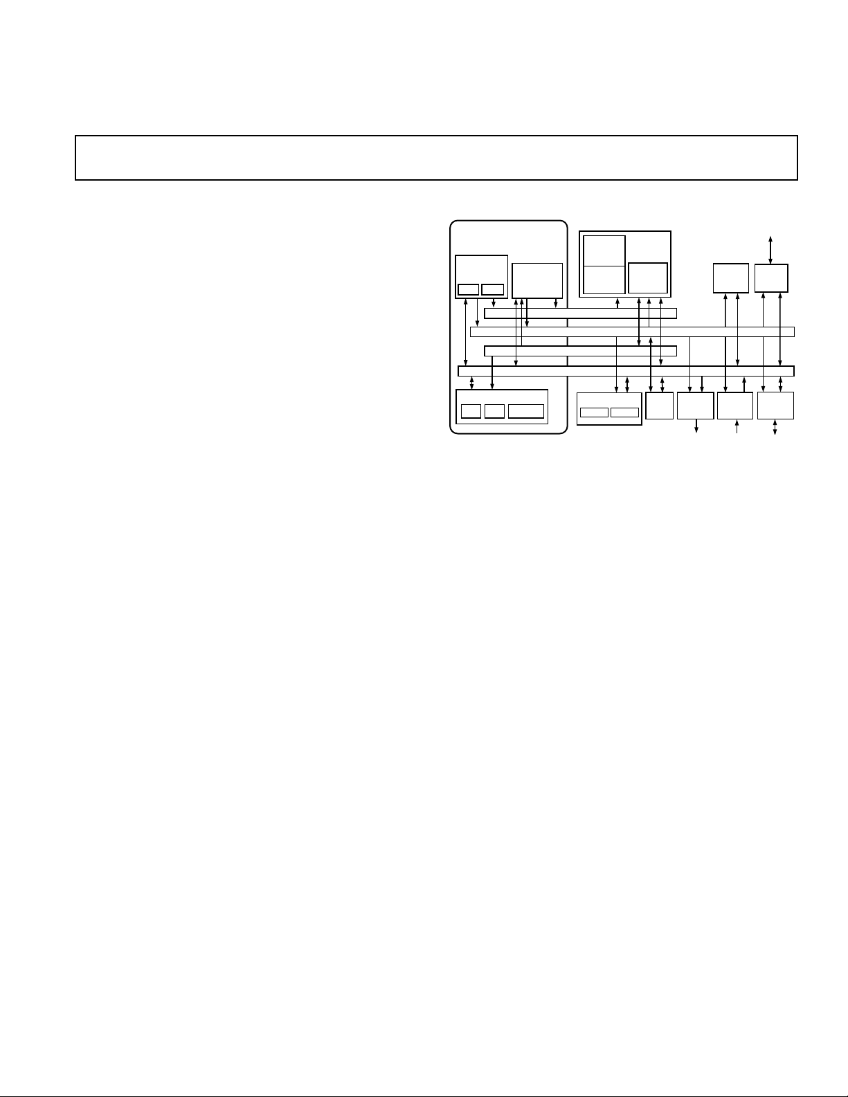
FUNCTIONAL BLOCK DIAGRAM
ADSP-2100 BASE
ARCHITECTURE
DATA
ADDRESS
GENERATORS
DAG 1 DAG 2
ARITHMETIC UNITS
ALU
PROGRAM
SEQUENCER
PROGRAM MEMORY ADDRESS
PROGRAM MEMORY DATA
DATA MEMORY DATA
SHIFTER
MAC
DATA MEMORY ADDRESS
GENERAL DESCRIPTION
The ADMC330 is a low cost single chip DSP microcontroller
optimized for stand alone ac motor control applications. The
device is based on a 20 MHz fixed-point DSP core (ADSP-
2171) and a set of motor control peripherals including seven
analog input channels and a 12-bit three-phase PWM generator.
The device has two auxiliary 8-bit PWM channels and adds
expansion capability through the serial ports and an 8-bit digital
I/O port. The ADMC330 has internal 2K words program RAM,
and 1K words data RAM, which can be loaded from an external
device via the serial port. There are also 2K words of internal
program ROM, which includes a monitor that adds software
debugging features through the serial port.
The ADMC330 core combines the ADSP-2100 base architecture (three computational units, data address generators and a
program sequencer) with two serial ports, a programmable
timer, extensive interrupt capabilities and on-chip program and
data memory.
In addition, the ADMC330 supports new instructions, which
include bit manipulations—bit set, bit clear, bit toggle, bit test—
new ALU constants, new multiplication instruction (x squared),
biased rounding and global interrupt masking, for increased
flexibility.
PROGRAM
ROM
2K 3 24
PROGRAM
RAM
2K 3 24
SERIAL PORTS
SPORT 0 SPORT 1
MEMORY
DATA
MEMORY
1K 3 16
TIMER
2 3 8-BIT
AUX
PWM
WATCH-
DOG
TIMER
ANALOG
INPUTS
8-BIT
PIO
12-BIT
3-PHASE
PWM
REV. 0
Information furnished by Analog Devices is believed to be accurate and
reliable. However, no responsibility is assumed by Analog Devices for its
use, nor for any infringements of patents or other rights of third parties
which may result from its use. No license is granted by implication or
otherwise under any patent or patent rights of Analog Devices.
One Technology Way, P.O. Box 9106, Norwood, MA 02062-9106, U.S.A.
Tel: 781/329-4700 World Wide Web Site: http://www.analog.com
Fax: 781/326-8703 © Analog Devices, Inc., 1997
Page 2

ADMC330–SPECIFICA TIONS
(VDD = 5 V 6 10%, GND = SGND = 0 V, TA = –408C to +858C, unless otherwise noted)
Parameter Min Typ Max Units Conditions/Comments
ANALOG-TO-DIGITAL CONVERTER Charging Capacitor = 1000 pF
2.5 kHz Sample Frequency
Signal Input 0.3 3.2
1
V
Resolution 12 Bits No Missing Codes
Converter Linearity 2 4 Bits
Zero Offset 50 200 mV
Channel-to-Channel Comparator Match 25 mV
Comparator Delay 600 ns
Current Source 9.5 11 13.5 µA
Current Source Linearity 3 %
ELECTRICAL CHARACTERISTICS
Logic Low 0.8 V
V
IL
Logic High 2 V
V
IH
Low-Level Output Voltage 0.4 V IOL = 2 mA
V
OL
Low-Level Output Voltage (XTAL) 0.5 V IOL = 2 mA
V
OL
High-Level Output Voltage 4 V I
V
OH
Low-Level Input Current –10 µAV
I
IL
High-Level Input Current 10 µAV
I
IH
= 0.5 mA
OH
= 0 V
IN
= V
IN
DD
IDDSupply Current (Power-Down Mode) 5 mA
IDDSupply Current (Static) 60 mA
CLOCK
Input Clock (t
) 100 ns 10 MHz Clock Input (CLKIN)
CK
DSP Clock (tCK/2) 50 ns 20 MHz DSP Clock (CLKOUT)
REFERENCE VOLTAGE OUTPUT
Voltage Level 2.2 2.55 2.9 V 100 µA Load
Output Voltage Change T
12-BIT PWM TIMER
Counter Resolution 12
MIN
to T
MAX
20 mV
2
Bits
Edge Resolution 100 ns 10 MHz CLKIN
Programmable Deadtime Range 0 12.5 µs 10 MHz CLKIN
Programmable Deadtime Increments 200 ns 10 MHz CLKIN
Programmable Pulse Deletion Range 0 12.5 µs 10 MHz CLKIN
Programmable Pulse Deletion Increments 100 ns 10 MHz CLKIN
PWM Frequency Range 2.5 kHz 10 MHz CLKIN
PWMSYNC Pulsewidth (T
)2µs 10 MHz CLKIN
CRST
Gate Drive Chop Frequency Range 0.08 5 MHz 10 MHz CLKIN
AUXILIARY PWM TIMERS
Resolution 8 Bits
PWM Frequency 39 kHz 1/256 of 10 MHz CLKIN Clock
NOTES
1
Signal input max V = 3.5 if VDD = 5 V ± 5%.
2
Resolution varies with PWM switching frequency (10 MHz Clock), 25 kHz = 8 bits, 2.5 kHz = 12 bits.
Specifications subject to change without notice.
–2– REV. 0
Page 3
WARNING!
ESD SENSITIVE DEVICE
ABSOLUTE MAXIMUM RATINGS*
Supply Voltage (VDD) . . . . . . . . . . . . . . . . . .–0.3 V to +7.0 V
Digital Input Voltage . . . . . . . . . . . . . . . . . . . . . –0.3 V to V
Analog Input Voltage . . . . . . . . . . . . . . . . . . . . . –0.3 V to V
Analog Reference Input Voltage . . . . . . . . . . . . –0.3 V to V
Digital Output Voltage Swing . . . . . . . . . . . . . . –0.3 V to V
Analog Reference Output Swing . . . . . . . . . . . . –0.3 V to V
DD
DD
DD
DD
DD
Operating Temperature . . . . . . . . . . . . . . . . . –40°C to +85°C
Lead Temperature (Soldering, 10 sec) . . . . . . . . . . . .+280°C
*Stresses greater than those listed above may cause permanent damage to the
device. These are stress ratings only; functional operation of the device at these or
any other conditions greater than those indicated in the operational sections of this
specification is not implied. Exposure to absolute maximum rating conditions for
extended periods may affect device reliability.
ORDERING GUIDE
Temperature Instruction Package Package
Model Range Rate Description Option
ADMC330BST –40°C to +85°C 20 MHz 80-Lead Plastic Thin Quad Flatpack (TQFP) ST-80
CAUTION
ESD (electrostatic discharge) sensitive device. Electrostatic charges as high as 4000 V readily
accumulate on the human body and test equipment and can discharge without detection.
Although the ADMC330 features proprietary ESD protection circuitry, permanent damage may
occur on devices subjected to high energy electrostatic discharges. Therefore, proper ESD
precautions are recommended to avoid performance degradation or loss of functionality.
ADMC330
–3–REV. 0
Page 4
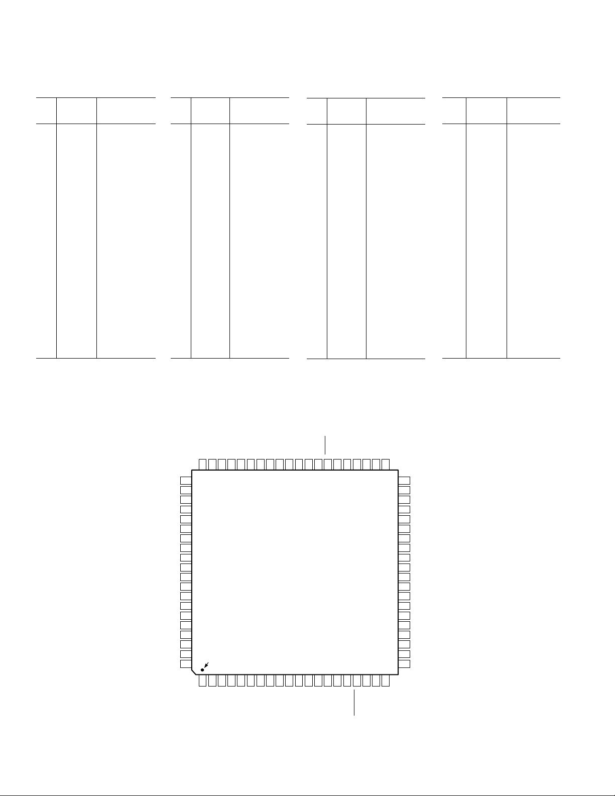
ADMC330
PIN FUNCTION DESCRIPTIONS
Pin Pin Pin
No. Type Name
1NC
2 I/P VAUX3
3 O/P REFOUT
4 SUP V
DD
5 GND GND
6 BIDIR PIO7
7 BIDIR PIO6
8 BIDIR PIO5
9 BIDIR PIO4
10 BIDIR PIO3
11 BIDIR PIO2
12 BIDIR PIO1
13 BIDIR PIO0
14 O/P AUX1
15 O/P AUX0
16 SUP V
DD
17 I/P PWMTRIP
18 GND GND
19 NC
20 NC
Pin Pin Pin
No. Type Name
21 NC
22 SUP V
DD
23 GND GND
24 NC
25 O/P PWMSYNC
26 O/P CL
27 O/P CH
28 O/P BL
29 O/P BH
30 O/P AL
31 O/P AH
32 NC
33 SUP V
DD
34 GND GND
35 GND GND
36 GND GND
37 GND GND
38 GND GND
39 NC
40 NC
PIN CONFIGURATION
80-Lead Plastic Thin Quad Flatpack (TQFP)
(ST-80)
Pin Pin Pin
No. Type Name
41 NC
42 GND GND
43 GND GND
44 I/P XTAL
45 I/P CLKIN
46 I/P PWMPOL
47 I/P RESET
48 GND GND
49 SUP V
DD
50 O/P CLKOUT
51 GND GND
52 O/P DT1
53 BIDIR TFS1
54 BIDIR RFS1
55 I/P DR1A
56 I/P DR1B
57 BIDIR SCLK1
58 BIDIR DT0
59 NC
60 NC
Pin Pin Pin
No. Type Name
61 NC
62 NC
63 BIDIR TFS0
64 BIDIR RFS0
65 BIDIR DR0
66 BIDIR SCLK0
67 SUP V
DD
68 GND GND
69 GND AGND
70 I/P CAPIN
71 O/P ICONST
72 GND SGND
73 I/P V1
74 I/P V2
75 I/P V3
76 I/P VAUX0
77 I/P VAUX1
78 I/P VAUX2
79 NC
80 NC
61
NC
62
NC
63
TFS0
64
RFS0
65
DR0
66
SCLK0
V
67
DD
68
GND
69
AGND
70
CAPIN
ICONST
71
72
SGND
73
V1
74
V2
75
V3
VAUX0
76
VAUX1
77
78
VAUX2
NC
79
80
NC
NC = NO CONNECT
NC
DT0
NC
SCLK1
DR1B
DR1A
60
59585756555453525150494847
RFS1
TFS1
DT1
GND
CLKOUT
ADMC330
TOP VIEW
(Not to Scale)
PIN 1
IDENTIFIER
2
3
1
NC
VAUX3
REFOUT
4
DD
V
5
GND
6
PIO7
7
PIO6
8
PIO5
9
PIO4
10
PIO3
11
PIO2
DD
V
12
PIO1
GND
13
PIO0
RESET
PWMPOL
46
15
14
AUX1
AUX0
XTAL
CLKIN
454443
16
17
DD
V
PWMTRIP
GND
18
GND
GND
42
19
NC
NC
41
20
NC
40
NC
39
NC
38
GND
37
GND
36
GND
35
GND
34
GND
33
V
32
NC
31
AH
30
AL
29
BH
28
BL
27
CH
26
CL
25
PWMSYNC
24
NC
23
GND
V
22
NC
21
DD
DD
–4– REV. 0
Page 5

ADMC330
The ADMC330 operates with a 50 ns instruction cycle time.
Every instruction can execute in a single processor cycle.
The flexible architecture and comprehensive instruction set of
the ADMC330 allow the processor to perform multiple operations in parallel. In one processor cycle the ADMC330 can:
• generate the next program address
• fetch the next instruction
• perform one or two data moves
• update one or two data address pointers
• perform a computational operation
This takes place while the processor continues to:
• receive and transmit data through the two serial ports
• decrement the timer
Independently the peripheral blocks can:
• generate three-phase PWM waveforms for a power inverter
• generate two signals using the 8-bit auxiliary PWM timers
• acquire four analog signals
• control eight digital I/O lines
• decrement the watchdog timer
ROM Code Functions
The ADMC330 has a 2K Boot ROM that contains the
following:
• Monitor Program:
Serial Boot Loader for OTP ROM or EEPROM
UART Debugger Interface and Loader
• Math Utilities/Tables:
Sine, cosine, tangent, inverse tangent, log, inverse log,
square root, 1/X, 1/(sine rms), unsigned division, Cartesian
to polar conversion, interpolation
The ADMC330 is similar to an ADSP-2172 in its booting sequence. The MMAP and BMODE pins are tied high, which
enables the on-chip ROM and starts execution of the monitor
program on power-up or reset. The monitor program first attempts to boot load through SPORT1 from a serial memory
device. The loader uses a two-wire (data and clock) serial protocol. The ADMC330 provides a serial clock to the device equal
to 1/20 of CLKOUT. Default input is from a Xilinx XC1765D
OTP ROM or Atmel AT17C65 EEPROM; other devices are
possible as long as they adhere to the loader protocol. If the
serial load is successful, the code that was downloaded is executed at the start of user memory space.
Failing a synchronous boot load, the ADMC330 monitor switches
over to debug mode and waits for commands over SPORT1
from a UART. Debug mode uses a standard RS-232 protocol in
which only the data receive and transmit lines are used by the
ADMC330. This interface is used by the Visual DSP
®
Debugger,
but can also be used by UART devices for boot loading programs.
In addition to the monitor program, the ROM contains the
previously listed math utilities. These routines can be called
from user applications.
Development System
The ADSP-2100 Family Development Software, a complete set
of tools for software and hardware system development, supports the ADMC330. The system builder provides a high level
method for defining the architecture of systems under development. The assembler has an algebraic syntax that is easy to
program and debug. The linker combines object files into
Visual DSP is a registered trademark of Analog Devices, Inc.
–5–REV. 0
an executable file. The simulator provides an interactive
instruction-level simulation with a reconfigurable user interface
to display different portions of the hardware environment. A
MAKEPROM utility splitter generates PROM programmer
compatible files. The C Compiler, based on the Free Software
Foundation’s GNU C Compiler, generates ADMC330 assembly source code. The runtime library includes over 100 ANSIstandard mathematical and DSP-specific functions.
Low cost, easy-to-use hardware development tools include an
ADMC330-EVAL board and a windows based software debugger.
This debugger can be run with either the ADMC330-EVAL
board or the target system by communicating over a two-wire
asynchronous link to a PC.
FUNCTIONAL DESCRIPTION
ADMC330 Peripherals Overview
The ADMC330 set of peripherals was specifically developed to
address the requirements of variable speed control of ac induction motors (ACIM) and electronically commutated synchronous motors (ECM). They are memory mapped to a block in
the DSP data memory space allowing single cycle read and/or
write to all peripheral registers. The operation of the peripherals
is synchronized to the DSP core by a clock HCLK, which is
derived from half of the DSP system clock.
Three-Phase PWM Generator
• 12-bit center-based PWM generator including programmable deadtime and narrow pulse deletion.
• ECM crossover block.
• Output enable block.
• Hardwired output polarity control.
• External trip input.
• Pulsed PWM output capability for transformer coupled gate.
Analog I/O
• Two 8-bit PWM Output Timers—(Synthesized Analog
Output).
• Comparator based Analog Input Acquisition. Analog-to-digital
conversion is accomplished via 4-channel single slope ADC.
Digital I/O
• Eight bits of programmable digital I/O configurable as
interrupt sources.
THREE-PHASE PWM GENERATOR
The ADMC330 PWM controller is a self-contained programmable waveform generator that produces PWM switching signals for a three-phase power inverter. It includes a waveform
timing edge calculation unit which allows the generation of six
center based PWM signals based on only three duty cycle register updates every switching cycle. This minimizes the DSP
software required to service the PWM controller and frees up
processor time for the motor control law implementation. In the
default configuration it produces the three-phase center based
PWM waveforms required for three phase sinusoidal inverter.
However, it can also be configured for space vector modulation
schemes, or for controlling brushless dc motors (sometimes
known as electronically commutated motors). It also has functions which simplify the interface to the power inverter gate
drive and protection circuits.
The PWM controller is synchronized to the DSP core by the
HCLK which runs at half the DSP clock frequency giving waveform resolution of 100 ns with a 20 MHz DSP clock. There are
Page 6
ADMC330
four configuration registers (PWMTM, PWMDT, PWMPD
and PWMGATE), which define basic waveform parameters
such as the master switching frequency, deadtime, minimum
pulsewidth, and gate drive chopping. There PWM output signals on the pins AH through CL are controlled by the input
registers (PWMCHA, PWMCHB, PWMCHC and PWMSEG)
and the control pins PWMTRIP and PWMPOL.
PWM Controller Overview
The PWM controller consists of three units: the center-based
timing unit, output control unit and the gate drive unit as shown
in Figure 1.
• The center-based PWM timing unit is the core of the PWM
controller and produces three pairs of complemented and
deadtime adjusted PWM waveforms as required for ac motor
control.
• The output control unit is a signal switching unit that selects
the appropriate PWM signals to be connected to the output
pins based on the bits set in the segment register (PWMSEG)
as may be required for ECM control or some space vector
modulation schemes.
• The gate drive block sets the logic polarity of the PWM “on”
signal according to the polarity of the PWMPOL pin to match
the gate drive circuit requirement. It can also modulate the
PWM “on” signal with a high frequency carrier (0.08 MHz–
5 MHz) if required for a transformer coupled gate drive circuit.
The DSP-based control algorithm can be synchronized to the
PWM generator by a hardware interrupt signal that is generated
at the end of every PWM switching cycle. This same PWMSYNC
signal is internally connected to the internal analog-to-digital
converter and is also available at an output pin. Finally, the
hardware PWMTRIP pin can be used to shut down the PWM
controller in the event of a fault.
Center-Based PWM Timing Unit
The center-based PWM timing unit is a programmable timer
that generates three pairs of fixed frequency PWM waveforms
suitable for controlling a three-phase power inverter. The unit
contains arithmetic circuits that calculate the PWM signal timing edges from waveform parameters such as the PWM period,
dead time and the duty cycle for each inverter phase. There is
no extra DSP software overhead once the duty cycle for each
phase has been calculated and loaded into the PWM channel
registers.
The PWM Timing Unit produces three pairs of complemented
variable duty cycle waveforms symmetrical about common axes
of the form shown in Figure 2. They are complemented waveforms, which means that for any pair of PWM waveforms (AH
and AL), they can never both be ON at the same time. They are
deadtime adjusted, which means that for any pair of PWM
waveforms, there is a delay between switching from being ON in
one waveform to being ON in the complemented waveform. A
pulse deletion function is implemented, which means that very
narrow PWM pulses will not be generated.
It is important to note that the deadtime compensation does not
take place on the boundary between consecutive PWM cycles.
Thus both the low side and high side devices can switch on
during the transition from a full-ON state to any other state.
This potentially volatile condition can be avoided by:
• Ensuring that the device never enters to the full-ON or fullOFF states, that is,
PWMCHx ≤ PWMTM –2 × (PWMDT + 1), with PWMPD = 0
• Using an external deadtime compensation circuit.
There is an active high PWMSYNC pulse produced at the beginning of each PWM cycle to synchronize the operation of
other peripherals with the switching of the power inverter. This
signal is also internally connected to the ADC block to initiate
conversions, and to the DSP core to generate an interrupt.
Figure 2 shows the center-based PWM operation.
The master switching frequency can range from 2.5 kHz to
25 kHz and is an integral fraction of HCLK clock frequency. It
is set by the value in the 12-bit PWMTM period register, which
sets the total number of clock cycles in a PWM cycle. The
required PWM period as a function of the desired master
switching frequency (f
quency (f
) is given by:
HCLK
) and peripheral system clock fre-
PWM
f
PWMTM =
HCLK
f
PWM
HCLK
PWMSYNC
INTERRUPT
SIGNALS
TIMING CONTROL
REGISTERS
PWMTM
PWMDT
PWMPD
CENTER-BASED
CLK SYNC RESET
REGISTERS
PWM TIMING
UNIT
CHANNEL
PWMCHA
PWMCHB
PWMCHC
OUTPUT CONTROL
REGISTER
PWMSEG
OUTPUT
CONTROL
UNIT
SYNC
Figure 1. PWM Controller Overview
–6– REV. 0
GATE CONTROL
GATE CONTROL
REGISTER
REGISTER
PWMGATE
GATE
DRIVE
UNIT
CLK
AH
AL
BH
BL
CH
CL
PWMPOL
PWMSYNC
PWMTRIP
Page 7

ADMC330
For example, the HCLK clock is 10 MHz. If 8 kHz PWM
waveforms are required, then PWMTM should be loaded
with 10 MHz/8 kHz = 1250. A value must be written to the
PWMTM register before the PWM block can be used.
The ON time of each pair of PWM waveforms, e.g., AH and AL,
is set by the integer value in the duty cycle registers PWMCHA,
PWMCHB and PWMCHC. The deadtime between the active
portions of complementary waveforms is set by the value in the
deadtime register PWMDT and is subtracted from the value in
the duty cycle register. The final deadtime adjusted fractional
duty cycle for Channel A for example is given by:
t
PWMCHA – PWMDT
Aon
dA=
T
PWM
=
PWMTM
The minimum pulsewidth delivered is set by the value in the
pulse deletion register PWMPD. When the calculated high or
low pulsewidth for any channel is less than PWMPD, the
switching pulse is eliminated and the outputs are saturated one
to 100% high, and the other to 100% low.
START END
PWMCHA
Output Control Unit
The Output Control Unit contains special features that allow
the ADMC330 to be easily applied for the control of electronically commutated motors (ECM) or brushless dc motors
(BDCM). In these machines, only two motor phases are required
to conduct simultaneously so that at most two power switches are
turned on at any time. In order to build up current in the motor
phases, it is necessary to turn on the upper switch in one phase and
the lower switch in another phase of the inverter.
The PWMSEG register of the ADMC330 PWM block allows
modification of the pulsewidth modulation signals from the
center-based block in order to meet the requirements for ECM
control. Three bits of the PWMSEG register (Bits 6, 7 and 8)
permit individual crossover of the three PWM signal pairs. For
example, setting Bit 8 will crossover the signals for Phase A such
that the high-side signal from the center-based block will ultimately appear at the low-side output pin (AL). Conversely, the
low-side signal from the center-based block will appear at Pin AH.
BL
CH
CL
PWMSYNC
AH
AL
BH
PWMDT
PWMDT
PWMCHB
PWMDT
PWMCHC
PWMDT PWMDT
PWMTM
PWMDT
Figure 2. Three-Phase Center-Based Active Low PWM Waveforms
–7–REV. 0
Page 8

ADMC330
Similar modifications can be made to Phases B and C using Bits
7 and 6, respectively, of the PWMSEG register. Six bits of the
PWMSEG register (Bits 0...5) are used to independently
enable/disable any individual PWM output pins. For example,
setting Bits 0 and 1 high disables PWM outputs CH and CL,
which keeps these outputs off over the full PWM period regardless of the value in the PWMCHC register. This feature is not
only useful for ECM control, but is also required in some space
vector modulation schemes. Modifications to the PWMSEG
register only become effective at the start of each PWM cycle. In
the transparent (default) mode, all bits in PWMSEG are set low.
Consider the situation shown in Figure 3 for operation of an
ECM with the AH and BL power devices active. The PWM
duty cycle registers, PWMCHA and PWMCHB, are programmed
with the appropriate on-time value. Since all three PWM registers must be written to trigger an update of the PWM, it is necessary to write also to PWMCHC. For this example, the particular
value written to this register is unimportant. Subsequently,
crossover bit of the PWMSEG register for Phase B (Bit 7) is set
to enable crossover of the Phase B signals. The PWM outputs
for Phase C high and low, Phase B high and Phase A low are
disabled by setting Bits 0, 1, 2 and 5 of the PWMSEG register.
In this example, the appropriate value for the PWMSEG register
is 0x00A7. In addition, high side chopping of the signal AH is
enabled by setting Bit 8 of the PWMGATE register.
CENTER-
BASED
OUTPUTS
AH
AL
BH
BL
CH
CL
MIDPOINT
PWMCHA
PWMCHB
PWMDT
PWMDT
ENDSTART
Figure 3. PWM Output Waveforms for an ECM with
Inverter Devices AH and BL Active
Known limitation of the ECM block. Modifying the PWMSEG
register while the PWM duty cycle transitions from a full-ON
state to any other state will cause both the high side and low
side devices to switch on for 50 ns. This potentially volatile
condition can be avoided by:
• Disabling the PWM channel outputs during the transition
from full-ON to any other state.
• Preventing the full-ON condition namely limiting PWMCHx to:
PWMCHx ≤ PWMTM –2 × (PWMDT + 1), with PWMPD = 0.
• Preventing a PWMSEG update operation during the transi-
tion from full-ON to any other state.
Gate Drive Unit
The Gate Drive Unit adds features that simplify the interface to
a variety of gate drive circuits for PWM inverters. If a transformer coupled power device gate drive amplifier is used, the
active PWM signal must be chopped at a high frequency of up
to 5 MHz. The chopped active PWM signals may be required
for the high side drivers only or for both high side and low side.
The gate drive chopping feature is enabled by Bits 8 and 9 of the
PWMGATE register. Setting Bit 8 enables a chopped PWM
signal on all high side output pins AH, BH and CH, setting
Bit 9 enables a chopped PWM signal on all low side output pins
AL, BL and CL. The gate chopping frequency is programmed
using Bits 0–5 of the PWMGATE register. The gate drive chopping frequency is given by the following equation:
f
f
=
chop
2×(GATETM +1)
HCLK
where GATETM is the 6-bit value in Bits 0...5 of the
PWMGATE register.
Depending on the type of power device gate drive circuit used,
either active high or active low, PWM signals will be required,
so an external PWM polarity pin is provided. The polarity of the
PWMPOL pin determines the active polarity of the PWM output signals (i.e., a low PWMPOL pin means active low PWM).
This must be set by hardware because even though the ADMC330
will power up with all PWM outputs off, the correct polarity of
an off PWM signal is a function of the gate drive circuit only.
The level on the PWMPOL pin is available in Bit 2 of the
SYSSTAT register.
External PWM Trip
In fault conditions the power devices must be switched off as soon
as possible after the fault has been detected, hence an external
hardware PWM trip input is provided. A low going PWMTRIP
pulse will reset the PWM block which will disable all PWM
outputs. This will also generate a PWMTRIP interrupt signal
and cause a DSP interrupt. The PWMTRIP pin is accessible
through Bit 0 of SYSSTAT so that the DSP can determine
when the external fault has been cleared. At this point, a full
initialization of the PWM controller will be required to restart
the PWM.
ADC OVERVIEW
The analog input block is a 12-bit resolution analog data acquisition system. A single slope type ADC is implemented by timing
the crossover between the analog input and a sawtooth reference ramp. A simple voltage comparator is used to latch the output
of a reference counter timer circuit when the crossover is detected.
There are seven input channels to the ADC of which three (V1,
V2 and V3) have dedicated comparators. The remaining four
inputs (VAUX0, VAUX1, VAUX2 and VAUX3) are multiplexed into the fourth comparator channel. This allows four
conversions per PWM period to be performed by the ADC. The
particular input signal that is fed to the fourth comparator input
is selected using the ADCMUX0 and ADCMUX1 bits of the
peripheral control register, MODECTRL. The settings of these
two control bits in order to select the appropriate auxiliary analog input is shown in Table I.
–8– REV. 0
Page 9

ADMC330
REFOUT
ICONST
CAPIN
C
SGND
VAUX0
VAUX1
VAUX2
VAUX3
ADC
TIMER
BLOCK
ADC1
ADC2
ADC3
ADCAUX
ADMUX0
ADMUX1
4-1
MUX
V3
V1
V2
PWMSYNC
ADC REGISTERS
HCLK
ADC1
ADC3
PWMGATE
PWMSEG
1 = ENABLE
0 = DISABLE
1 = CROSSOVER
0 = NO CROSSOVER
15 14 13 12 11 10 9 8 7 6 5 4 3 2 1 0
LOW SIDE GATE CHOPPING
HIGH SIDE GATE CHOPPING
15 14 13 12 11 10 9 8 7 6 5 4 3 2 1 0
A CHANNEL CROSSOVER
B CHANNEL CROSSOVER
C CHANNEL CROSSOVER
Figure 4. Configuration of PWMSEG and PWMGATE Registers
Table I. ADC Auxiliary Channel Selection
MODECTRL (1) MODECTRL (0)
Select ADCMUX1 ADCMUX0
VAUX0 0 0
VAUX1 0 1
VAUX2 1 0
VAUX3 1 1
Analog Block
The operation of the ADC block may be explained by reference
to Figures 5 and 6. The reference ramp is tied to one input of
each of the four comparators. This reference ramp is generated
by charging an external timing capacitor with a constant current
source. The timing capacitor is connected between pins CAPIN
and SGND. The capacitor voltage is reset at the start of each
PWM cycle using the PWMSYNC pulse, which is held high for
20 CLKIN cycles (T
= 2 µs for a 10 MHz CLKIN). On the
CRST
falling edge of PWMSYNC, the capacitor begins to charge at a
rate determined by the capacitor and the current source values.
An internal current source is made available for connection to
the external timing capacitor on the ICONST pin. An external
current source could also be used, if required. The four input
comparators of the ADC block continuously compare the values
of the four analog inputs with the capacitor voltage. Each comparator output will go high when the capacitor voltage exceeds
the respective analog input voltage.
ADC Timer Block
The ADC timer block consists of a 12-bit counter clocked at a
constant rate of HCLK, equal to half the DSP clock rate. This
gives a timer resolution of 100 ns at the maximum CLKIN
frequency of 10 MHz. The counter is reset on the falling edge of
the PWMSYNC pulse so that the counter commences at the
beginning of the reference voltage ramp. When the output of a
given comparator goes high, the counter value is latched into the
–9–REV. 0
GATETM
GATE DRIVE CHOPPING FREQUENCY
)/(2(GATETM+1))
(f
HCLK
CH OUTPUT DISABLE
CL OUTPUT DISABLE
BH OUTPUT DISABLE
BL OUTPUT DISABLE
AH OUTPUT DISABLE
AL OUTPUT DISABLE
1 = DISABLE
0 = ENABLE
appropriate 12-bit ADC register. There are four ADC registers
(ADC1, ADC2, ADC3 and ADCAUX) corresponding to each
of the four comparators. At the end of the reference voltage
ramp, all four registers should have been loaded with new values
so that new conversion data is available to the controller after a
PWMSYNC interrupt.
The first set of values loaded into the output registers after the
first PWMSYNC interrupt will be invalid since the latched value
is indeterminate. For very low analog inputs, less than the minimum reference value, the comparator output will be permanently high and the output register will contain the code 0x000.
Also, if the input analog voltage exceeds the peak capacitor
ramp voltage, the comparator output will be permanently low
and a 0xFFF code will be produced. This indicates an input
overvoltage condition.
Figure 5. ADC Overview
Page 10

ADMC330
V
VIL
PWMSYNC
T
t
PWM
As a result, assuming ± 10% variations in both the capacitance
V
C
V
CMAX
and current source, the nominal capacitance value required at a
given PWM period is:
V1
C
NOM
(0.9× I
=
CONST
(1 .1)(3.5)
)(T
PWM–TCRST
)
The largest standard value capacitor that is less than this calculated value is chosen. Table III shows the appropriate standard
capacitor value to use for various PWM switching frequencies
t
VIL
– T
CRST
T
CRST
assuming ±10% variations in both the current source and capacitor tolerances. If required, more precise control of the ramp
voltage is possible by using higher precision capacitor components, an external current source and/or series or parallel timing
capacitor combinations.
COMPARATOR
OUTPUT
Figure 6. Analog Input Block Operation
ADC Resolution
Because the operation of the ADC is intrinsically linked to the
PMW block, the effective resolution of the ADC is a function of
the PMW switching frequency. The effective ADC resolution is
determined by the rate at which the counter timer is clocked.
For a CLKIN period of t
and a PWM period of T
CK
PWM
, the
maximum count of the ADC is given by
T
Max Count =
PWM
t
CK
For an assumed CLKIN frequency of 10 MHz, the effective
resolution of the ADC block is tabulated for various PWM
switching frequencies in Table II.
Table II. ADC Resolution Examples
PWM Frequency Effective Resolution
(kHz) Max Count (Bits)
2.5 3980 ≈12
4 2480 >11
8 1230 >10
18 535 >9
25 380 >8
External Timing Capacitor
In order to maximize the useful input voltage range and effective
resolution of the ADC, it is necessary to carefully select the
value of the external timing capacitor. For a given capacitance
value, C
where I
T
CRST
, the peak ramp voltage is given by:
NOM
I
()
VCmax =
is the nominal current source value of 10.5 µA and
CONST
CONSTTPWM–TCRST
C
NOM
is the PWMSYNC pulsewidth. In selecting the capacitor
value, however, it is necessary to take into account the tolerance
of the capacitor and the variation of the current source value.
To ensure that the full input range of the ADC is utilized, it is
necessary to select the capacitor so that at the maximum capacitance value and the minimum current source output, the ramp
voltage will charge to at least 3.5 V.
Table III. Timing Capacitor Selection
PWM Frequency Timing Capacitor
(kHz) (pF)
2.5–3.0 820
3.0–3.6 680
3.6–4.3 560
4.3–5.2 470
5.2–6.2 390
6.2–7.3 330
7.3–9.0 270
9.0–10.9 220
10.9–13.2 180
13.2–15.8 150
15.8–19.6 120
19.6–23.4 100
23.4–28.2 82
AUXILIARY PWM TIMERS OVERVIEW
The two auxiliary PWM timers can be used to produce analog
signal outputs when configured as PWM DACs. This allows the
ADMC330 to generate a reference for power factor correction
and supply an analog reference for other systems in the application. They can also be used as supplementary PWM outputs for
other control circuits.
The PWM timers generate two fixed frequency edge-based
variable duty cycle PWM signals. The PWM frequency is
1/256 times HCLK, or 39 kHz. The duty cycle is based on a
user-supplied 8-bit value loaded into the AUX0 and AUX1
registers.
The timer output can range from 0% to 99.6%, where the number written to the register represents the high time. The values
are updated as soon as new values are written in the registers: if
the value is smaller than the present counter value the output
goes low, otherwise it stays high.
On RESET, the AUX0 and AUX1 registers are cleared to zero
and remain at zero until a new value is written.
PWM DAC Equation
The PWM output must be filtered in order to produce a low
frequency analog signal between 0 V to 4.98 V dc. For example,
a 2-pole filter with a 1.2 kHz cut off frequency will sufficiently
attenuate the PWM carrier. Figure 7 shows how the filter would
be applied.
–10– REV. 0
Page 11

ADMC330
PWMDAC
R1 R2
C1
R1 = R2 = 13kV
C1 = C2 = 10nF
C2
Figure 7. Auxiliary PWM Output Filter
PROGRAMMABLE DIGITAL INPUT/OUTPUT
The ADMC330 has eight programmable digital I/O (PIO) pins:
PIO0–PIO7. Each pin can be individually configurable as either
an input or an output. Input pins can also be used to generate
interrupts.
The PIO pins are configured as input or output by setting the
appropriate bits in the PIODIR register, as shown in Figure 8.
The read/write register PIODATA is used to set the state of an
output pin or read the state of an input pin. Writing to PIODATA
affects only the pins configured as outputs. The default state,
after an ADMC330 reset, is that all PIO are configured as inputs.
Any pin can be configured as an independent edge triggered
interrupt source. The pin must first be configured as an input
and then the appropriate bit must be set in the PIOINTEN
register. A peripheral interrupt is generated when the input level
changes on any PIO pin configured as an interrupt source. A
PIO interrupt sets the appropriate bit in the PIOFLAG register.
The DSP peripheral interrupt service routine (ISR) must read
the PIOFLAG registers to determine which PIO pin was the
source of the PIO interrupt. Reading the PIOFLAG register will
clear it.
WATCHDOG TIMER OVERVIEW
The watchdog timer can be used to reset the DSP and peripherals in the event of a software error hanging the processor. The
watchdog timer is enabled by writing a value to the watchdog
timer register. In the event of the code “hanging” the counter
will count down from its initial value to zero and the watchdog
timer hardware will force a DSP and peripheral reset. In normal
operation a section of DSP code will write to the timer register
to reset the counter to its initial value preventing it from reaching zero.
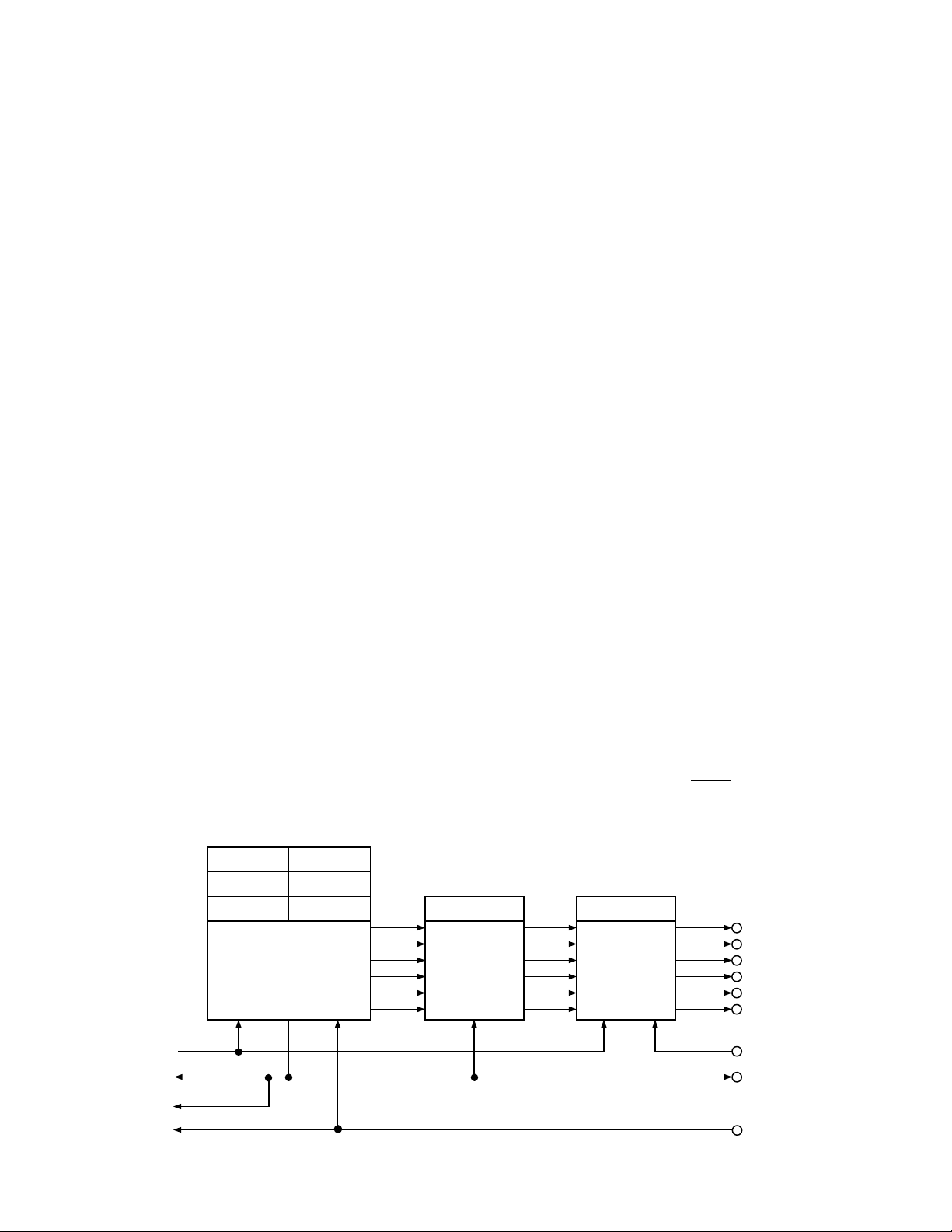
DSP CORE ARCHITECTURE OVERVIEW
Figure 9 is a block diagram of the ADMC330 processor core
and system peripherals. The processor contains three independent computational units: The ALU, the multiplier/accumulator
(MAC) and the shifter. The computational units process 16-bit
data directly and have provisions to support multiprecision
computations. The ALU performs a standard set of arithmetic
and logic operations; division primitives are also supported. The
MAC performs single-cycle multiply, multiply/add and multiply/
subtract operations with 40 bits of accumulation. The shifter
performs logical and arithmetic shifts, normalization, denormalization and derive exponent operations. The shifter can be used to
efficiently implement numeric format control including multiword and block floating-point representations.
The internal result (R) bus directly connects the computational
units so that the output of any unit may be the input of any unit
on the next cycle.
PIODIR
15 14 13 12 11 10 9 8 7 6 5 4 3 2 1 0
PIODATA
15 14 13 12 11 10 9 8 7 6 5 4 3 2 1 0
15 14 13 12 11 10 9 8 7 6 5 4 3 2 1 0
15 14 13 12 11 10 9 8 7 6 5 4 3 2 1 0
(READ/WRITE)
PIOINTEN
(WRITE-ONLY)
PIOFLAG
(READ-ONLY)
1 = OUTPUT
1 = OUTPUT
0 = INPUT
0 = INPUT
1 = HI
0 = LOW
1 = ENABLE INTERRUPT
0 = DISABLE INTERRUPT
1 = INTERRUPT FLAGGED
0 = NO INTERRUPT
PIO0
Figure 8. Configuration of PIO Registers
–11–REV. 0
PIO7
Page 12

ADMC330
INSTRUCTION
REGISTER
DATA
ADDRESS
GENERATOR
#1
INPUT REGS
ALU MAC SHIFTER
OUTPUT REGS
DATA
ADDRESS
GENERATOR
#2
INPUT REGS
OUTPUT REGS
PROGRAM
SEQUENCER
16
R BUS
EXCHANGE
INPUT REGS
OUTPUT REGS
14
14
24
BUS
16
PROGRAM ROM
2K 3 24
PROGRAM SRAM
2K 3 24
Figure 9. DSP Core Block Diagram
A powerful program sequencer and two dedicated data address
generators ensure efficient delivery of operands to these computational units. The sequencer supports conditional jumps, subroutine calls and returns in a single cycle. With internal loop
counters and loop stacks, the ADMC330 executes looped code
with zero overhead; no explicit jump instructions are required to
maintain the loop.
Two data address generators (DAGs) provide addresses for
simultaneous dual operand fetches (from data memory and
program memory). Each DAG maintains and updates four
address pointers. Whenever the pointer is used to access data
(indirect addressing), it is post-modified by the value of one of
four possible modify registers. A length value may be associated
with each pointer to implement automatic modulo addressing
for circular buffers.
Efficient data transfer is achieved with the use of five internal
buses:
• Program Memory Address (PMA) Bus
• Program Memory Data (PMD) Bus
• Data Memory Address (DMA) Bus
• Data Memory Data (DMD) Bus
• Result (R) Bus
Program memory can store both instructions and data, permitting the ADMC330 to fetch two operands in a single cycle,
one from program memory and one from data memory. The
ADMC330 can fetch an operand from on-chip program memory
and the next instruction in the same cycle.
DATA
SRAM
CONTROL
LOGIC
PMA BUS
DMA BUS
PMD BUS
DMD BUS
TRANSMIT REG
RECEIVE REG
SERIAL
PORT 0
1K 3 16
COMPANDING
CIRCUITRY
TRANSMIT REG
RECEIVE REG
SERIAL
PORT 1
55
FLAGS
TIMER
The ADMC330 can respond to interrupts. There can be
internal interrupts generated by the Timer, the Serial Ports
(SPORTs), and software or peripheral interrupts generated by
the PIO or PWM. There is also a master RESET signal.
The two serial ports provide a complete synchronous serial
interface with optional companding in hardware and a wide
variety of framed or frameless data transmit and receive modes
of operation. Each port can generate an internal programmable
serial clock or accept an external serial clock.
Boot circuitry provides for automatically loading on-chip program memory from the data input and output pins on SPORT1.
SPORT1 can be alternatively configured as an input flag, output
flag or two additional interrupt sources.
A programmable interval timer generates periodic interrupts. A
16-bit count register (TCOUNT) is decremented every n processor cycles, where n-l is a scaling value stored in an 8-bit register (TSCALE). When the value of the count register reaches
zero, an interrupt is generated and the count register is reloaded
from a 16-bit period register (TPERIOD).
The ADMC330 instruction set provides flexible data moves and
multifunction (one or two data moves with a computation)
instructions. Every instruction can be executed in a single processor cycle. The ADMC330 assembly language uses an algebraic syntax for ease of coding and readability. A comprehensive
set of development tools supports program development.
–12– REV. 0
Page 13

ADMC330
Serial Ports
The ADMC330 incorporates two complete synchronous serial
ports (SPORT0 and SPORT1) for serial communications and
multiprocessor communication.
Following is a brief list of the capabilities of the ADMC330
SPORTs. Refer to the ADSP-2100 Family User’s Manual for
further details.
• SPORTs are bidirectional and have a separate, double-buffered transmit and receive section.
• SPORTs can use an external serial clock or generate their
own serial clock internally.
• SPORTs have independent framing for the receive and transmit sections. Sections run in a frameless mode or with frame
synchronization signals internally or externally generated.
Frame sync signals are active high or inverted, with either of
two pulsewidths and timings.
• SPORTs support serial data word lengths from 3 to 16 bits
and provide optional A-law and µ-law companding according
to CCITT recommendation G.711.
• SPORT receive and transmit sections can generate unique
interrupts on completing a data word transfer.
• SPORTs can receive and transmit an entire circular buffer of
data with only one overhead cycle per data word. An interrupt
is generated after a data buffer transfer.
• SPORT0 has a multichannel interface to selectively receive
and transmit a 24- or 32-word, time-division multiplexed,
serial bit stream.
• SPORT1 can be configured to have two external interrupts
(IRQ0 and IRQ1) and the Flag In and Flag Out signals. The
internally generated serial clock may still be used in this
configuration.
• SPORT1 has two multiplexed data receive pins DR1A and
DR1B. DR1A is automatically selected at boot up and is the
default input for the serial ROM. For UART communication
DR1B is selected.
A full description of the SPORT timing parameters is given in
Figure 14.
Interrupts
The interrupt controller allows the processor core to respond to
nine possible interrupts with the minimum of overhead. The
ADMC330 supports eight internal interrupts from the timer,
the two serial ports, the software interrupts, and the software
forced power-down interrupt. The ninth interrupt, IRQ2 on the
2171 core, is actually wired internally to the ADMC330 peripheral interrupt sources. This peripheral interrupt is generated on
a PWM trip, PWMSYNC (once each PWM cycle), or from any
of the eight PIO ports. The PWMSYNC interrupt is triggered
by a low to high transition on the PWMSYNC pulse.
The PWMTRIP interrupt is triggered on a high-to-low transition on the PWMTRIP pin. A PIO interrupt is detected on any
change of state (high-to-low or low-to-high) on the PIO line.
When a peripheral interrupt is detected, a flag bit is set in the
IRQFLAG register for PWMSYNC and PWMTRIP or in the
PIOFLAG register for a PIO interrupt, and the IRQ2 line is
pulled low. The IRQ2 line is held low until all pending peripheral interrupts are acknowledged. Execution then begins at the
IRQ2 (or peripheral) interrupt vector location (0x004). Software at this location further determines if the source of the
interrupt was a PWM trip, PWYMSYNC, or PIO, by reading
the IRQFLAG register, and vectors to the appropriate interrupt
vector location. If more than one interrupt occurs simultaneously,
the higher priority interrupt service routine is executed. The
software at location 0x004 is provided in a default interrupt
vector table that is created by the on-chip boot ROM code.
Therefore, a user need only put the interrupt service routine
for the given interrupt at the interrupt vector location shown in
Table IV. Reading the IRQFLAG register clears the PWMTRIP
and PWMSYNC bits and acknowledges the interrupt, thus
allowing further interrupts when the interrupt service routine
exits. When the IRQFLAG register is read, it is saved in a data
memory variable so the user interrupt service routines can check
to see if there were simultaneous PWMTRIP and PWMSYNC
interrupts.
A user’s PIO interrupt service routine must read the PIOFLAG
register to determine which PIO port is the source of the interrupt. Reading the PIOFLAG register clears all bits in the
register and acknowledges the interrupt, thus allowing further
interrupts when the interrupt service routine exits.
All interrupts are internally prioritized and individually maskable
(except for power-down). The interrupt vector locations and
priorities for all interrupts are listed in Table IV. Interrupts can
be masked or unmasked with the IMASK register. Individual
interrupt requests are logically ANDed with the bits in IMASK;
the higher priority unmasked interrupt is then selected. The
software forced power-down interrupt is nonmaskable. The
ADMC330 masks all interrupts for one instruction cycle following the execution of an instruction that modifies the IMASK
register. This does not affect autobuffering.
Table IV. Interrupt Priority and Interrupt Vector Addresses
Interrupt
Source of Interrupt Vector Location (Hex)
Reset 0x0000 (Reserved)
PWMTRIP and Power-Down* 0x002C (Highest Priority)
PWMSYNC* 0x000C
PIO* 0x0008
SPORT0 Transmit 0x0010
SPORT0 Receive 0x0014
Software Interrupt 1 0x0018
Software Interrupt 0 0x001C
SPORT1 Transmit or IRQ1 0x0020
SPORT1 Receive or IRQ0 0x0024
Timer 0x0028 (Lowest Priority)
*Peripheral interrupt (IRQ2) starts execution at 0x004, software further vector
to 0x002C, 0x000C or 0x0008 as appropriate.
–13–REV. 0
Page 14

ADMC330
10MV
CLKIN XTAL
The interrupt control register, ICNTL, allows the external interrupts to be either edge- or level-sensitive. Since the IRQ2 line is
a combination of all peripheral interrupt sources, they will all be
set to edge- or level-sensitive. Level-sensitive is recommended
when using both PIO and PWM interrupts together. When
simultaneous PIO and PWM interrupts occur, the IRQ2 line is
brought low and held low until both the PIO and PWM interrupts are acknowledged. If interrupts are set to edge-sensitive
only, one IRQ2 interrupt will occur for simultaneous interrupts
and it is incumbent on the interrupt service routine to check for
simultaneous interrupts. If, however, interrupts are set to levelsensitive, all simultaneous interrupts are detected because IRQ2
is held low until all interrupts are acknowledged.
The ICNTL register also allows interrupts to be sequentially
processed or nested with higher priority interrupts taking precedence. Since the peripheral interrupts are all on the same level
(IRQ2), they can only be nested by manually unmasking them
with the IMASK register from inside the interrupt service routine.
The IFC register is a write-only register, which is used to force
and clear interrupts from software.
On-chip stacks preserve the processor status and are automatically maintained during interrupt handling. The stacks are 12
levels deep to allow interrupt nesting. A set of shadow registers
are provided for single context switching.
Power-Down
The ADMC330 can be put in a lower power state from software
control by setting the PDFORCE bit in the SPORT1 Autobuffer/
Power-Down register. This causes a power-down interrupt;
execution then continues at the power-down interrupt vector
location 0x002C. The power-down interrupt vector location is
shared with the PWMTRIP interrupt, thus if a different interrupt service routine is required, the vector must be changed
prior to setting the PDFORCE bit. The power-down interrupt
service routine must perform a peripheral reset prior to entering
power-down to shut down the PWM signals to the motor. The
interrupt service routine can then perform any housekeeping
operations prior to executing an IDLE instruction, after which
the ADMC330 is in power-down mode. The only way out of
power-down is to perform a hardware reset of the ADMC330.
Clock Signals
The ADMC330 can be clocked by either a crystal or a TTLcompatible clock signal.
The CLKIN input cannot be halted, changed during operation
or operated below the specified frequency during normal operation.
If an external clock is used, it should be a TTL-compatible
signal running at half the instruction rate. The signal is connected to the processor’s CLKIN input. When an external clock
is used, the XTAL input must be left unconnected.
The ADMC330 uses an input clock with a frequency equal to
half the instruction rate; a 10 MHz input clock yields a 50 ns
processor cycle (which is equivalent to 20 MHz). Normally,
instructions are executed in a single processor cycle. All device
timing is relative to the internal instruction clock rate, which is
indicated by the CLKOUT signal when enabled.
Because the ADMC330 includes an on-chip oscillator circuit,
an external crystal may be used. The crystal should be connected across the CLKIN and XTAL pins, with two capacitors
connected as shown in Figure 10. A parallel-resonant, fundamental frequency, microprocessor-grade crystal should be used.
Figure 10. External Crystal Connections
A clock output (CLKOUT) signal is generated by the processor
at the processor’s cycle rate.
Reset
The RESET signal initiates a master reset of the ADMC330.
The RESET signal must be asserted during the power-up sequence to assure proper initialization. RESET during initial
power-up must be held long enough to allow the internal clock
to stabilize. If RESET is activated any time after power-up, the
clock continues to run and does not require stabilization time.
The power-up sequence is defined as the total time required for
the crystal oscillator circuit to stabilize after a valid V
DD
is applied to the processor, and for the internal phase-locked loop
(PLL) to lock onto the specific crystal frequency. A minimum of
2000 CLKIN cycles ensures that the PLL has locked, but does
not include the crystal oscillator start-up time. During this
power-up sequence the RESET signal should be held low.
The RESET input contains some hysteresis; however, if you
use an RC circuit to generate your RESET signal, the use of an
external Schmitt trigger is recommended.
The master reset sets all internal stack pointers to the empty
stack condition, masks all interrupts and clears the MSTAT
register. When RESET is released, the DSP starts running from
the internal ROM and the boot loading sequence is performed.
If an SROM (serial ROM) or Serial EEPROM is connected to
SPORT1 with valid program data, this code is then loaded and
execution starts. If a valid device is not detected, then the program defaults to debug mode with SPORT1 configured as a
UART running at 9600 baud.
–14– REV. 0
Page 15

ADMC330
A software controlled full peripheral reset (including the watchdog timer) is achieved by toggling the DSP FL2 flag from 1 to 0
to 1 again.
MEMORY MAP
The ADMC330 has two types of memory: data memory and
program memory. Program RAM starts at 0x0000, while the
program ROM area starts at 0x800. The data RAM starts at
0x3800 while the peripherals are mapped to a data memory
block starting at 0x2000.
Table V. Program Memory
0x0000–0x002F Interrupt Vector Table
0x0030–0x07FF User Program Space
0x0800–0x0BFF ROM Monitor
0x0C00–0x0FFF ROM Math Utilities
Table VI. Data Memory
0x2000–0x201F Peripherals
0x3800–0x3B8F User Data Space
0x3B90–0x3BFF Reserved for ROM Monitor Use
ADMC330 Registers
Some registers store values. For example, AX0 stores an ALU
operand; I4 stores a DAG2 pointer. Other registers consist of
control bits and fields, or status flags. For example, ASTAT
contains status flags from arithmetic operations, and fields in
DWAIT control the numbers of wait states for different zones of
data memory.
A secondary set of registers in all computational units allows a
single-cycle context switch.
The bit and field definitions for control and status registers are
given in the rest of this section, except for IMASK, ICNTL and
IFC, which are defined earlier in this data sheet. The system
control register, timer registers and SPORT control registers are
all mapped into data memory; that is, registers are accessed by
reading and writing data memory locations rather than register
names. The particular data memory address is shown with each
memory-mapped register.
Biased Rounding
A new mode allows biased rounding in addition to the normal
unbiased rounding. When the BIASRND bit is set to 0, the
normal unbiased rounding operations occur. When the BIASRND
bit is set to 1, biased rounding occurs instead of the normal unbiased rounding. When operating in biased rounding mode all
rounding operations with MR0 set to 0x8000 will round up,
rather than only rounding odd MR1 values up. For example:
MR value before RND biased RND result unbiased RND result
00-0000-8000 00-0001-8000 00-0000-8000
00-0001-8000 00-0002-8000 00-0002-8000
00-0000-8001 00-0001-8001 00-0001-8001
00-0001-8001 00-0002-8001 00-0002-8001
00-0000-7FFF 00-0000-7FFF 00-0000-7FFF
00-0001-7FFF 00-0001-7FFF 00-0001-7FFF
This mode only has an effect when the MR0 register contains
0x8000; all other rounding operation work normally. This mode
was added to allow more efficient implementation of bit specified algorithms that specify biased rounding, such as the GSM
speech compression routines. Unbiased rounding is preferred
for most algorithms.
Note: BIASRND bit is Bit 12 of the SPORT0 Autobuffer
Control register.
INSTRUCTION SET DESCRIPTION
The ADMC330 assembly language instruction set has an
algebraic syntax that was designed for ease of coding and readability. The assembly language, which takes full advantage of the
processor’s unique architecture, offers the following benefits:
• The algebraic syntax eliminates the need to remember
cryptic assembler mnemonics. For example, a typical arithmetic add instruction, such as AR = AX0 + AY0, resembles a
simple equation.
• Every instruction assembles into a single, 24-bit word that can
execute in a single instruction cycle.
• The syntax is a superset ADSP-2100 Family assembly language and is completely source and object code compatible
with other family members.
• Sixteen condition codes are available. For conditional jump,
call, return or arithmetic instructions, the condition can be
checked and the operation executed in the same instruction
cycle.
• Multifunction instructions allow parallel execution of an arithmetic instruction with up to two fetches or one write to processor memory space during a single instruction cycle.
Consult the ADSP-2100 Family User’s Manual for a complete
description of the syntax and an instruction set reference with
particular reference to the ADSP-2171 device.
Interrupt Enable
The ADMC330 supports an interrupt enable instruction. Interrupts are enabled by default at reset. The instruction source
code is specified as follows:
Syntax: ENA INTS;
Description: Executing the ENA INTS instruction allows
all unmasked interrupts to be serviced again.
Interrupt Disable
The ADMC330 supports an interrupt disable instruction. The
instruction source code is specified as follows:
Syntax: DIS INTS;
Description: Reset enables interrupt servicing. Executing
the DIS INTS instruction causes all interrupts to be masked without changing the
contents of the IMASK register. Disabling
interrupts does not affect the autobuffer circuitry, which will operate normally whether
or not interrupts are enabled. The disable
interrupt instruction masks all user interrupts
including the power-down interrupt.
–15–REV. 0
Page 16

ADMC330
ICNTL
43210
0
IRQ0 SENSITIVITY
IRQ1 SENSITIVITY
IRQ2 SENSITIVITY
INTERRUPT NESTING
1 = ENABLE, 0 = DISABLE
15 14 13 12 11 10 9 8 7 6 5 4 3 2 1 0
0000000000000000
IRQ2
1 = EDGE
0 = LEVEL
SPORT0 TRANSMIT
SPORT0 RECEIVE
IFC
15 14 13 12 11 10 9 8 7 6 5 4 3 2 1 0
0000000000000000
INTERRUPT FORCE
SPORT0 TRANSMIT
SPORT0 RECEIVE
SPORT1 TRANSMIT OR IRQ1
SPORT1 RECEIVE OR IRQ0
IRQ2
SOFTWARE 1
SOFTWARE 0
TIMER
Figure 11. Interrupt Registers
SYSTEM CONTROLLER OVERVIEW
The System Controller has a number of functions:
1. It decodes the DSP address bus and selects the appropriate
peripheral registers.
2. It controls the ADC multiplexer select lines.
3. It can enable PWMTRIP and PWMSYNC interrupts.
4. It controls the SPORT0 multiplexer select lines.
5. It resets the peripherals and control registers on hardware,
software or watchdog initiated resets.
6. It handles interrupts generated by the peripherals and
generates a DSP core interrupt signal IRQ1 (IRQ2).
7. It can be used to control the peripheral test modes.
IMASK
1 = ENABLE, 0 = DISABLE
TIMER
IRQ0 OR SPORT1 RECEIVE
IRQ1 OR SPORT1 TRANSMIT
SOFTWARE 0
SOFTWARE 1
INTERRUPT CLEAR
TIMER
SPORT1 RECEIVE OR IRQ0
SPORT1 TRANSMIT OR IRQ1
SOFTWARE 0
SOFTWARE 1
SPORT0 RECEIVE
SPORT0 TRANSMIT
IRQ2
DSP INTERFACE AND MEMORY MAP
All data transferred between the DSP core and the peripherals is
controlled by the System Controller.
The peripheral registers, with the exception of the ADC read
registers, are right justified, i.e., the LSB of each register is
connected to the LSB of the 16-bit DSP DM data bus DSPD
[15:0]. Any unused MSBs are connected to zeros. The ADMC
peripheral registers are memory mapped to 32 words on the
DSP address space, starting at DSP memory location 0x2000:
1. ADC read registers (0–3)
2. PIO Registers (4–7)
3. PWM Set-Up Registers (8–11)
4. PWM Data Registers (12–15)
5. AUX PWM Data Registers (16, 17)
6. System Registers (21–24)
–16– REV. 0
Page 17

ADMC330
Table VII. Peripheral Register Map
Address Offset
(HEX) (Decimal) Name Bits Used Function
0x2000 0 ADC1 [4..15] ADC Results for V1
0x2001 1 ADC2 [4..15] ADC Results for V2
0x2002 2 ADC3 [4..15] ADC Results for V3
0x2003 3 ADCAUX [4..15] ADC Results for VAUX
0x2004 4 PIODIR [0..7] PIO Pins Direction Setting
0x2005 5 PIODATA [0..7] PIO Pins Input/Output Data
0x2006 6 PIOINTEN [0..7] PIO Pins Interrupt Enable
0x2007 7 PIOFLAG [0..7] PIO Pins Interrupt Status
0x2008 8 PWMTM [0..11] PWM Period
0x2009 9 PWMDT [0..6] PWM Deadtime
0x200A 10 PWMPD [0..6] PWM Pulse Deletion Time
0x200B 11 PWMGATE [0..8] PWM Gate Drive Configuration
0x200C 12 PWMCHA [0..11] PWM Channel A Pulsewidth
0x200D 13 PWMCHB [0..11] PWM Channel B Pulsewidth
0x200E 14 PWMCHC [0..11] PWM Channel C Pulsewidth
0x200F 15 PWMSEG [0..8] PWM Segment Select
0x2010 16 AUX0 [0..7] AUX PWM Output 1
0x2011 17 AUX1 [0..7] AUX PWM Output 2
0x2012 18 Not Used
0x2013 19 Not Used
0x2014 20 Not Used
0x2015 21 MODECTRL [0..15] System Control Register
0x2016 22 SYSSTAT [0..1] System Status
0x2017 23 IRQFLAG [0..2] Interrupt Status
0x2018 24 WDTIMER [0..15] Watchdog Timer
0x2019..F 25..31 Not Used
Multiplexer, PWM Interrupts and SPORT1 Control
The ADC, the SPORT1 peripherals and the PWM interrupts
are configured using the MODECTRL register.
1. Two bits control the ADC aux channel selection:
ADCMUX0..1.
2. Two bits can enable/disable the PWMTRIP and PWMSYNC
interrupts.
3. Two bits control the SPORT1 UART and DR1A/B multiplexer.
The PWM interrupt enable bits are masking bits rather than
set/reset bits. Therefore, before enabling these interrupts any
pending interrupts can be cleared by reading the IRQFLAG
register.
Setting the UARTEN bit connects DR1 to the RFS1 input,
which allows SPORT1 to be used as a UART port. The DR1SEL
bit selects either pins DR1A or DR1B. The reset condition for
all bits in this register is zero.
ADMC330
SPORT1
DT1
DR1
TFS1
RFS1
SCLCK1
UART
ENABLE
SELECT
DR1B
DT1
DR1A
DR1B
TFS1
RFS1
SCLCK1
DEFAULT SWITCH
POSITION SHOWN
The DSP and Peripheral Reset Functions
A full system reset of the ADMC330 is achieved by pulling the
RESET pin low (for > 5 clock cycles when running, or > 2000
clock cycles on power-up). This resets the DSP core and all
peripherals including the watchdog timer.
The SYSSTAT register indicates the fault status of the ADMC330
after a PWMTRIP interrupt or a watchdog reset:
1. The status of the PWMTRIP pin (active low).
2. The status of the watchdog flag register (this is not reset on a
DSP RESET).
3. The status of the PWMPOL pin.
When one of the peripherals generates an interrupt, the DSP
IRQ2 line is pulled low and a flag bit is set in the IRQFLAG
register for PWMSYNC and PWMTRIP or in the PIOFLAG
register for a PIO interrupt. The DSP can read these registers to
determine the source of the interrupt. When the IRQFLAG
register is read, the PWMSYNC and PWMTRIP bits are
cleared to zero. Reading the PIOFLAG register clears all the bits
in this register to zero. When both registers are cleared, the IRQ2
line is set high again. The reset condition for all bits in this register is zero.
Figure 12. Internal Multiplexing of SPORT1 Pins
–17–REV. 0
Page 18

ADMC330
MODECTRL
15 14 13 12 11 10 9 8 7 6 5 4 3 2 1 0
(READ/WRITE)
SYSSTAT
15 14 13 12 11 10 9 8 7 6 5 4 3 2 1 0
ADC MUX CONTROL
00 = VAUX0
01 = VAUX1
10 = VAUX2
11 = VAUX3
PWMTRIP INTERRUPT ENABLE
PWMSYNC INTERRUPT ENABLE
SPORT1 DATA RECEIVE SELECT
SPORT1 MODE SELECT
1 = ENABLE
0 = DISABLE
1 = DR1B
0 = DR1A
1 = UART
0 = SPORT
PWMTRIP PIN STATUS
WATCHDOG STATUS
PWMPOL PIN STATUS
IRQFLAG
15 14 13 12 11 10 9 8 7 6 5 4 3 2 1 0
PWMTRIP INTERRUPT STATUS
PWMSYNC INTERRUPT STATUS
Figure 13. Configuration of MODECTRL, SYSSTAT and IRQFLAG Registers
1 = HI
0 = LO
1 = RESET OCCURRED
0 = NORMAL
1 = HI
0 = LO
1 = PENDING
0 = CLEARED
–18– REV. 0
Page 19

ADMC330
))
TIMING PARAMETERS
SERIAL PORTS
Frequency
12.5 MHz 13.0 MHz 13.824 MHz* Dependency
Parameter Min Max Min Max Min Max Min Max Unit
Timing Requirement:
SCLK Period 80 76.9 72.3 100 ns
t
SCK
DR/TFS/RFS Setup before SCLK Low 8 8 8 15 ns
t
SCS
DR/TFS/RFS Hold after SCLK Low 10 10 10 20 ns
t
SCH
SCLK
t
SCP
Switching Characteristic:
CLKOUT High to SCLK
t
CC
SCLK High to DT Enable 0 0 0 0 ns
t
SCDE
SCLK High to DT Valid 20 20 20 30 ns
t
SCDV
TFS/RFS
t
RH
TFS/RFS
t
RD
DT Hold after SCLK High 0 0 0 0 ns
t
SCDH
TFS (Alt) to DT Enable 0 0 0 0 ns
t
TDE
TFS (Alt) to DT Valid 18 18 18 25 ns
t
TDV
SCLK High to DT Disable 25 25 25 40 ns
t
SCDD
RFS (Multichannel, Frame Delay Zero) 20 20 20 30 ns
t
RDV
to DT Valid
Width 30 28 28 40 ns
IN
OUT
Hold after SCLK High 0 0 0 0 ns
OUT
Delay from SCLK High 20 20 20 30 ns
OUT
20 35 19.2 34.2 18.1 33.1 0.25 tCK0.25 t
+ 20 ns
CK
*Maximum serial port operating frequency is 13.824 MHz for all processor speed grades except the 12.5 MHz ADSP-2101 and 13.0 MHz ADSP-2111.
CLKOUT
SCLK
RFS
TFS
RFS
TFS
(ALTERNATE
FRAME MODE)
(MULTICHANNEL MODE,
FRAME DELAY 0 (MFD = 0
DR
IN
IN
OUT
OUT
DT
TFS
RFS
t
t
CC
t
RH
SCDE
t
TDE
t
t
RD
SCDV
t
t
TDV
RDV
t
CC
t
t
SCDD
t
t
SCH
SCS
t
SCDH
SCP
t
SCK
t
SCP
Figure 14. Serial Ports
–19–REV. 0
Page 20

ADMC330
OUTLINE DIMENSIONS
Dimensions shown in inches and (mm).
80-Lead Plastic Thin Quad Flatpack (TQFP)
(ST-80)
0.640 (16.25)
0.620 (15.75)
0.030 (0.75)
0.020 (0.50)
SEATING
PLANE
0.004
(0.10)
MAX
0.006 (0.15)
0.002 (0.05)
0.063 (1.60)
MAX
0.057 (1.45)
0.053 (1.35)
61
80
0.486 (12.35) TYP
60
1
0.029 (0.73)
0.022 (0.57)
0.553 (14.05)
0.549 (13.95)
TOP VIEW
(PINS DOWN)
0.014 (0.35)
0.010 (0.25)
41
40
21
20
0.553 (14.05)
0.549 (13.95
0.640 (16.25)
0.486 (12.35) TYP
0.620 (15.75)
C3043–2.5–9/97
–20–
PRINTED IN U.S.A.
REV. 0
 Loading...