

Page 1
a
Motion Coprocessor
ADMC201
FEATURES
Analog Input Block
11-Bit Resolution Analog-to-Digital (A/D) Converter
7 Single-Ended (SE) Analog Inputs
4 Simultaneously Sampled Analog Inputs
Expansion with 4 Multiplexed Inputs
3.2 s Conversion Time/Channel
0 V–5 V Analog Input Range
Internal 2.5 V Reference
PWM Synchronized Sampling Capability
12-Bit PWM Timer Block
Three-Phase Center-Based PWM
1.5 kHz–25 kHz PWM Switching Frequency Range
Programmable Deadtime
Programmable Pulse Deletion
PWM Synchronized Output
External PWM Shutdown
Vector Transformation Block
12-Bit Vector Transformations
Forward and Reverse Clarke Transformations
Forward and Reverse Park Rotations
2.9 s Transformation Time
Programmable Digital I/O Port
6-Bit Configurable Digital I/O
Change of State Interrupt Support
DSP & Microcontroller Interface
12 Bit Memory Mapped Registers
Twos Complement Data Format
6.25 MHz to 25 MHz Operating Clock Range
68-Pin PLCC Package
Single 5 V DC Power Supply
Industrial Temperature Range
GENERAL DESCRIPTION
The ADMC201 is a motion coprocessor that can be used with
either microcontrollers or digital signal processors (DSP). It
provides the functionality that is required to implement a digital
control system. In a typical application, the DSP or microcontroller performs the control algorithms (position, speed,
torque and flux loops) and the ADMC201 provides the necessary motor control functions: analog current data acquisition,
vector transformation, digital inputs/outputs, and PWM drive
signals.
PRODUCT HIGHLIGHTS
Simultaneous Sampling of Four Inputs
A four channel sample and hold amplifier allows three-phase
motor currents to be sampled simultaneously, reducing errors
from phase coherency. Sample and hold acquisition time is
1.6 µs and conversion time per channel is 3.2 µs (using a 12.5 MHz
system clock).
REV. B
Information furnished by Analog Devices is believed to be accurate and
reliable. However, no responsibility is assumed by Analog Devices for its
use, nor for any infringements of patents or other rights of third parties
which may result from its use. No license is granted by implication or
otherwise under any patent or patent rights of Analog Devices.
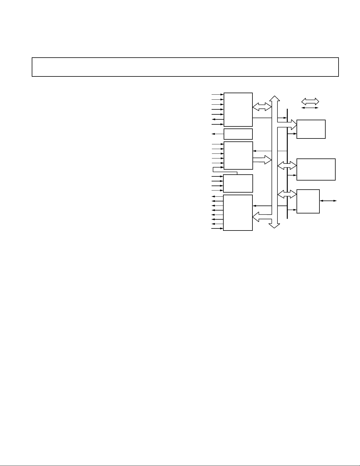
FUNCTIONAL BLOCK DIAGRAM
RESET
WR
A0–3
RD
CS
IRQ
CLK
REFOUT
REFIN
CONVST
AUX
AUX0
AUX1
AUX2
AUX3
PWMSYNC
AP
BP
CP
STOP
EMBEDDED
CONTROL
SEQUENCER
INTERNAL
REFERENCE
U
V
W
A
B
C
11-BIT
A/D
CONVERTER
MULTIPLEXER
EXPANSION
BLOCK
12-BIT
PWM TIMER
BLOCK
D0–D11
DATABUS
CONTROL BUS
CONTROL
REGISTERS
VECTOR
TRANSFORMATION
BLOCK
PROG.
DIGITAL
I/O
PORT
PIO 0–5
Flexible Analog Channel Sequencing
The ADMC201 supports acquisition of 2, 3, or 4 channels per
group. Converted channel results are stored in registers and
the data can be read in any order. The sampling and conversion
time for two channels is 8 µs, three channels is 11.2 µs, and four
channels is 14.4 µs (using a 12.5 MHz system clock).
Embedded Control Sequencer
The embedded control sequencer off-loads the DSP or microprocessor, reducing the instructions required to read analog
input channels, control PWM timers and perform vector transformations. This frees the host processor for performing control
algorithms.
Fast DSP/Microprocessor Interface
The high speed digital interface allows direct connection to 16-bit
digital signal processors and microprocessors. The ADMC201
has 12 bit memory mapped registers with twos complement
data format and can be mapped directly into the data memory
map of a DSP. This allows for a single instruction read and write
interface.
Integration
The ADMC201 integrates a four channel simultaneous sampling
analog-to-digital converter, four channel analog multiplexer,
analog reference, vector transformation, six digital inputs/outputs,
and three-phase PWM timers into a 68-pin PLCC. Integration
reduces cost, board space, power consumption, and design and
test time.
One Technology Way, P.O. Box 9106, Norwood, MA 02062-9106, U.S.A.
Tel: 781/329-4700 World Wide Web Site: http://www.analog.com
Fax: 781/326-8703 © Analog Devices, Inc., 2000
Page 2

(VDD = +5 V ⴞ 5%; AGND = DGND = 0 V; REFIN = 2.5 V; External Clock = 12.5 MHz;
ADMC201–SPECIFICATIONS
TA = –40ⴗC to +85ⴗC unless otherwise noted)
Parameter ADMC201AP Units Conditions/Comments
ANALOG-TO-DIGITAL CONVERTER
1
Resolution 11 Bits Twos Complement Data Format
Relative Accuracy ± 2 LSB max Integral Nonlinearity
Differential Nonlinearity ± 2 LSB max
Bias Offset Error ± 5 LSB max Any Channel
Bias Offset Match 4 LSB max Between Channels
Full-Scale Error ± 6 LSB max Any Channel
Full-Scale Error Match 4 LSB max Between Channels
Conversion Time/Channel 40 System CLK Cycles
Signal-to-Noise Ratio (SNR)
2
60 dB min fIN = 600 Hz Sine Wave, f
= 55 kHz, 600 Hz
SAMPLE
Channel-to-Channel Isolation
Two-/Three-Phase Mode –58 dB max Sine Wave Applied to Unselected Channels
Three-/Three-Phase Mode –55 dB max
ANALOG INPUTS
Input Voltage Level 0–5 Volts
Analog Input Current 100 µA max
Input Capacitance 10 pF typ
TRACK AND HOLD
Aperture Delay 200 ns max Any Channel
Aperture Time Delay Match 20 ns max Between Channels
SHA Acquisition Time 20 System CLK Cycles
Droop Rate 5 mV/ms max
REFERENCE INPUT
Voltage Level 2.5 V dc
Reference Input Current 50 µA max
REFERENCE OUTPUT
Voltage Level 2.5 Volts
Voltage Level Tolerance ± 5 % max Full Load
Drive Capability ± 200 µA max
LOGIC
V
IL
V
IH
V
OL
V
OH
0.8 V max
2.0 V min
0.4 V max I
4.5 V min I
= 400 µA, VDD = 5 V
SINK
= 20 µA, VDD = 5 V
SOURCE
Input Leakage Current 1 µA max
Three-State Leakage Current 1 µA max
Input Capacitance 20 pF typ
12-BIT PWM TIMERS
Resolution 12 Bits
Programmable Deadtime Range 0–10.08 µs
Programmable Deadtime Increments 2 System CLK Cycles 160 ns
Programmable Pulse Deletion Range 0–10.16 µs
Programmable Deletion Increments 1 System CLK Cycle 80 ns
Minimum PWM Frequency 1.5 kHz Resolution Varies with PWM Switching Frequency
(10 MHz Clock: 20 kHz = 9 Bits, 10 kHz = 10 Bits,
5 kHz = 11 Bits, 2.5 kHz = 12 Bits). Higher Frequencies are Available with Lower Resolution
VECTOR TRANSFORMATION Park & Clarke Transformation
Radius Error 0.7 % max
Angular Error 30 arc min max
Reverse Transformation Time 37 System CLK Cycles
Forward Transformation Time 40 System CLK Cycles
EXTERNAL CLOCK INPUT
Range 6.25–25 MHz If > 12.5 MHz, Then It Is Necessary to Divide Down
via SYSCTRL Register
INTERNAL SYSTEM CLOCK
Range 6.25–12.5 MHz
POWER SUPPLY CURRENT
I
DD
NOTES
1
Measurements made with external reference.
2
Tested with PWM Switching Frequency of 25 kHz.
Specifications subject to change without notice.
20 mA max
–2–
REV. B
Page 3
ADMC201
(
)
Table I. Timing Specifications (VDD = 5 V, ⴞ 5%; TA = –4
0ⴗC to +85ⴗC)
Number Symbol Timing Requirements Min Max Units
1t
2t
3t
4t
5t
6t
7t
8t
9t
10 t
11 t
12 t
13 t
14 t
15 t
16 t
17 t
18 t
19 t
20 t
21 t
22 t
23 t
24 t
NOTE
1
All WRITES to the ADMC201 must occur within 1 System Clock Cycle (0 wait states).
clk CLK Period 40 160 ns
per
clk CLK Pulsewidth, High 20 ns
pwh
clk CLK Pulsewidth, Low 20 ns
pwl
csb_wrb CS Low before Falling Edge of WR 0ns
su
addr_wrb ADDR Valid before Falling Edge of WR 0ns
su
data_wrb DATA Valid before Rising Edge of WR 13 ns
su
wrb_data DATA Hold after Rising Edge of WR 4.5 ns
hd
wrb_addr ADDR Hold after Rising Edge of WR 4.5 ns
hd
wrb_csb CS Hold after Rising Edge of WR 4.5 ns
hd
1
wrb
pwl
1
wrb
pwh
wrb_clk_h
hd
wrb_clk_h
su
wrb_clk_l
su
clk_wrb_l
hd
csb_rdb CS Low before Falling Edge of RD 0ns
su
addr_rdb ADDR Valid before Falling Edge of RD 0ns
su
rdb_addr ADDR Hold after Rising Edge of RD 0ns
hd
rdb_csb CS Hold after Rising Edge of RD 0ns
hd
rdb RD Pulsewidth, Low 20 ns
pwl
rdb RD Pulsewidth, High 20 ns
pwh
rdb_clk_h RD Low before Rising Edge of CLK 7.5 ns
su
rdb_clk_h RD Low after Rising Edge of CLK 7.5 ns
hd
resetb RESET Pulsewidth, Low 2 × t
pwl
1
1
1
1
9
WR Pulsewidth, Low 20 ns
WR Pulsewidth, High 20 ns
WR Low after Rising Edge of CLK 7 ns
WR High before Rising Edge of CLK 7 ns
WR High before Falling Edge of CLK 10 ns
WR High after Falling Edge of CLK 10 ns
clk ns
per
Number Symbol Switching Characteristics Min Max Units
25 t
26 t
27 t
28 t
RESET
rdb_data DATA Valid after Falling Edge of RD 23 ns
dly
rdb_data DATA Hold after Rising Edge of RD 0ns
hd
_pio Digital I/O Pulsewidth, High 2 × t
pwh
_pio Digital I/O Pulsewidth, Low 2 × t
pwl
CLK
1
2
3
CLK
CS
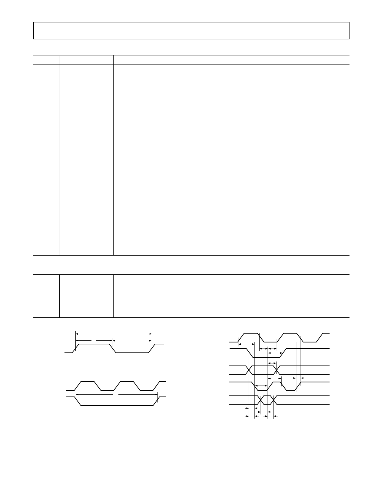
Figure 1. Clock Input Timing
A0–A3
CLK
24
WR
DATA
Figure 2. Reset Input Timing
12
NOTE:
ALL WRITES TO THE ADMC201 MUST OCCUR WITHIN
ONE SYSTEM CLOCK CYCLE
clk ns
per
clk ns
per
13
15
9
8
11
10
4
6
5
7
i.e., 0 WAIT STATES
14
Figure 3. Write Cycle Timing Diagram
REV. B
–3–
Page 4
ADMC201
WARNING!
ESD SENSITIVE DEVICE
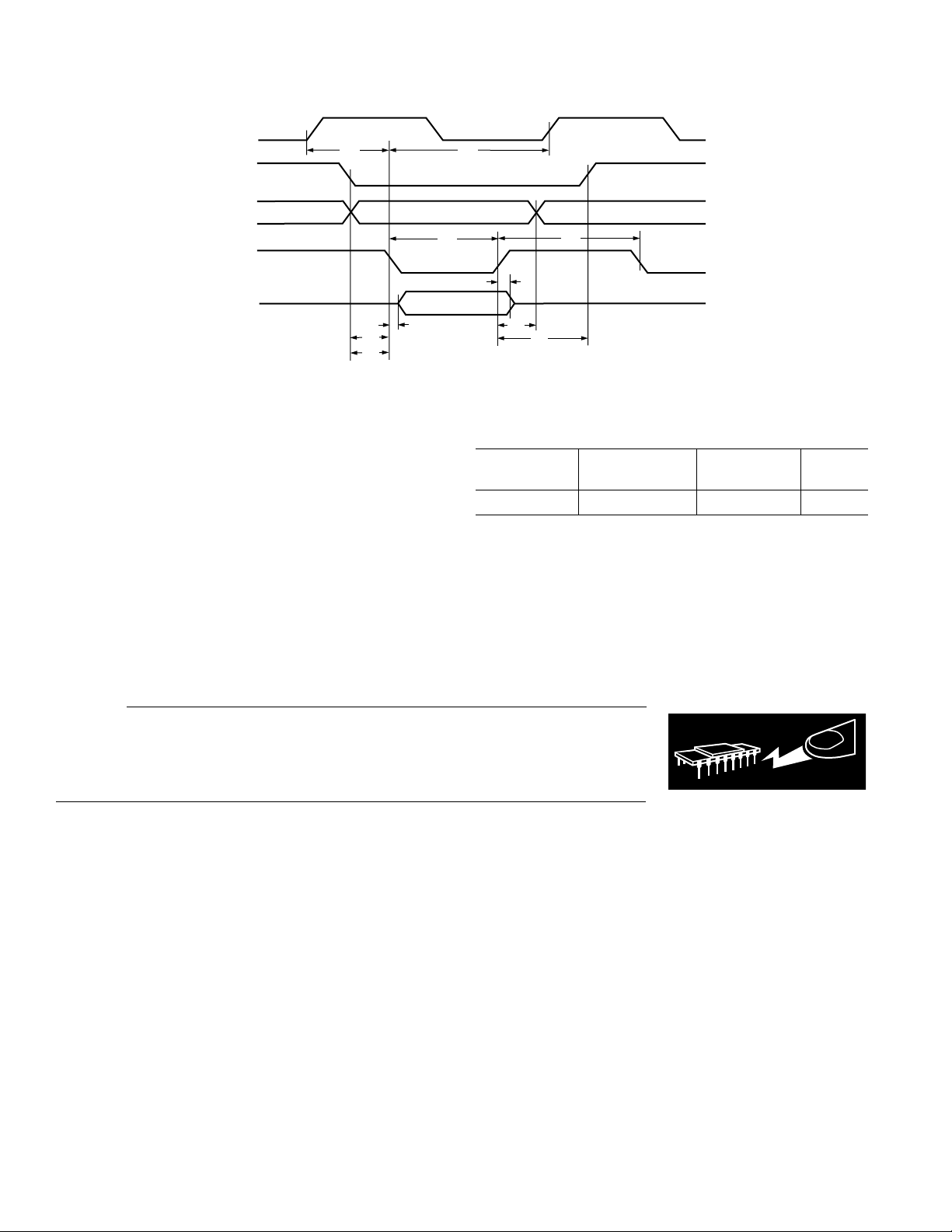
CLK
CS
A0–A3
RD
DATA
23
25
16
17
22
20
26
18
21
19
Figure 4. Read Cycle Timing Diagram
ABSOLUTE MAXIMUM RATINGS*
ORDERING GUIDE
Supply Voltage (VDD) . . . . . . . . . . . . . . . . . . –0.3 V to +7.0 V
Digital Input Voltage . . . . . . . . . . . . . . . . . . . . . –0.3 V to V
Analog Input Voltage . . . . . . . . . . . . . . . . . . . . . –0.3 V to V
Analog Reference Input Voltage . . . . . . . . . . . . –0.3 V to V
Digital Output Voltage Swing . . . . . . . . . . . . . . –0.3 V to V
Analog Reference Output Swing . . . . . . . . . . . . –0.3 V to V
Part Temperature Package Package
DD
Number Range Description Option
DD
DD
ADMC201AP –40°C to +85°C 68-Pin PLCC P-68A
DD
DD
Operating Temperature . . . . . . . . . . . . . . . . . –40°C to +85°C
Lead Temperature (Soldering, 10 sec) . . . . . . . . . . . . +280°C
*Stresses greater than those listed above may cause permanent damage to the
device. These are stress ratings only, and functional operation of the device at
these or any other conditions greater than those indicated in the operational
sections of this specification is not implied. Exposure to absolute maximum rating
conditions for extended periods may affect device reliability.
CAUTION
ESD (electrostatic discharge) sensitive device. Electrostatic charges as high as 4000 V readily
accumulate on the human body and test equipment and can discharge without detection.
Although the ADMC201 features proprietary ESD protection circuitry, permanent damage may
occur on devices subjected to high energy electrostatic discharges. Therefore, proper ESD
precautions are recommended to avoid performance degradation or loss of functionality.
–4–
REV. B
Page 5
PIN DESIGNATIONS
ADMC201
Pin Mnemonic Type Description
1 D9 BIDIR Data Bit 9
2 D10 BIDIR Data Bit 10
3 D11 BIDIR Data Bit 11, MSB
4 PIO0 BIDIR Programmable Digital I/O Bit 0
5 PIO1 BIDIR Programmable Digital I/O Bit 1
6 PIO2 BIDIR Programmable Digital I/O Bit 2
7 PIO3 BIDIR Programmable Digital I/O Bit 3
8 PIO4 BIDIR Programmable Digital I/O Bit 4
9 PIO5 BIDIR Programmable Digital I/O Bit 5
10 V
DD
11 A3 I/P Address Bit 3, MSB
12 A2 I/P Address Bit 2
13 A1 I/P Address Bit 1
14 A0 I/P Address Bit 0, LSB
15 NC No Connect
16 RESET I/P Chip Reset
17 CONVST I/P A/D Conversion Start
18 IRQ O/P Interrupt Request (Pull-Up Required)
19 V
DD
20 DGND GND Digital Ground
21 CLK I/P External Clock Input
22 WR I/P Write Select
23 RD I/P Output Enable/Read
24 CS I/P Chip Select
25 NC No Connect
26 V
DD
27 AGND GND Analog Ground
28 AGND GND Analog Ground
29 U I/P Analog Input U
30 V I/P Analog Input V
31 W I/P Analog Input W
32 SGND GND Analog Signal Ground
33 REFIN I/P Analog Reference Input
34 AUX3 I/P Auxiliary Analog Input 3
35 AUX2 I/P Auxiliary Analog Input 2
36 AUX1 I/P Auxiliary Analog Input 1
37 AUX0 I/P Auxiliary Analog Input 0
SUP +5 V Digital Power Supply
SUP +5 V Digital Power Supply
SUP +5 V Analog Power Supply
Pin Mnemonic Type Description
38 REFOUT O/P Internal 2.5 V Analog Reference
39 V
DD
SUP +5 V Digital Power Supply
40 DGND GND Digital Ground
41 DGND GND Digital Ground
42 DGND GND Digital Ground
43 DGND GND Digital Ground
44 V
DD
SUP +5 V Digital Power Supply
45 NC No Connect
46 DGND GND Digital Ground
47 STOP I/P PWM Timer Output Disable
48 PWMSYNC O/P PWM Synchronization Output
49 CP O/P PWM Timer Output C Prime
50 C O/P PWM Timer Output C
51 BP O/P PWM Timer Output B Prime
52 NC No Connect
53 B O/P PWM Timer Output B
54 AP O/P PWM Timer Output A Prime
55 A O/P PWM Timer Output A
56 DGND GND Digital Ground
57 DGND GND Digital Ground
58 DGND GND Digital Ground
59 V
DD
SUP +5 V Digital Power Supply
60 D0 BIDIR Data Bit 0, LSB
61 D1 BIDIR Data Bit 1
62 D2 BIDIR Data Bit 2
63 D3 BIDIR Data Bit 3
64 D4 BIDIR Data Bit 4
65 D5 BIDIR Data Bit 5
66 D6 BIDIR Data Bit 6
67 D7 BIDIR Data Bit 7
68 D8 BIDIR Data Bit 8
Pin Types Pin Types
I/P = Input Pin BIDIR = Bidirectional Pin
O/P = Output Pin SUP = Supply Pin
GND = Ground Pin
REV. B
10
V
DD
11
A3
12
A2
13
A1
14
A0
15
NC
16
RESET
17
CONVST
18
IRQ
19
V
DD
20
DGND
21
CLK
22
WR
23
RD
24
CS
25
NC
26
V
DD
NC = NO CONNECT
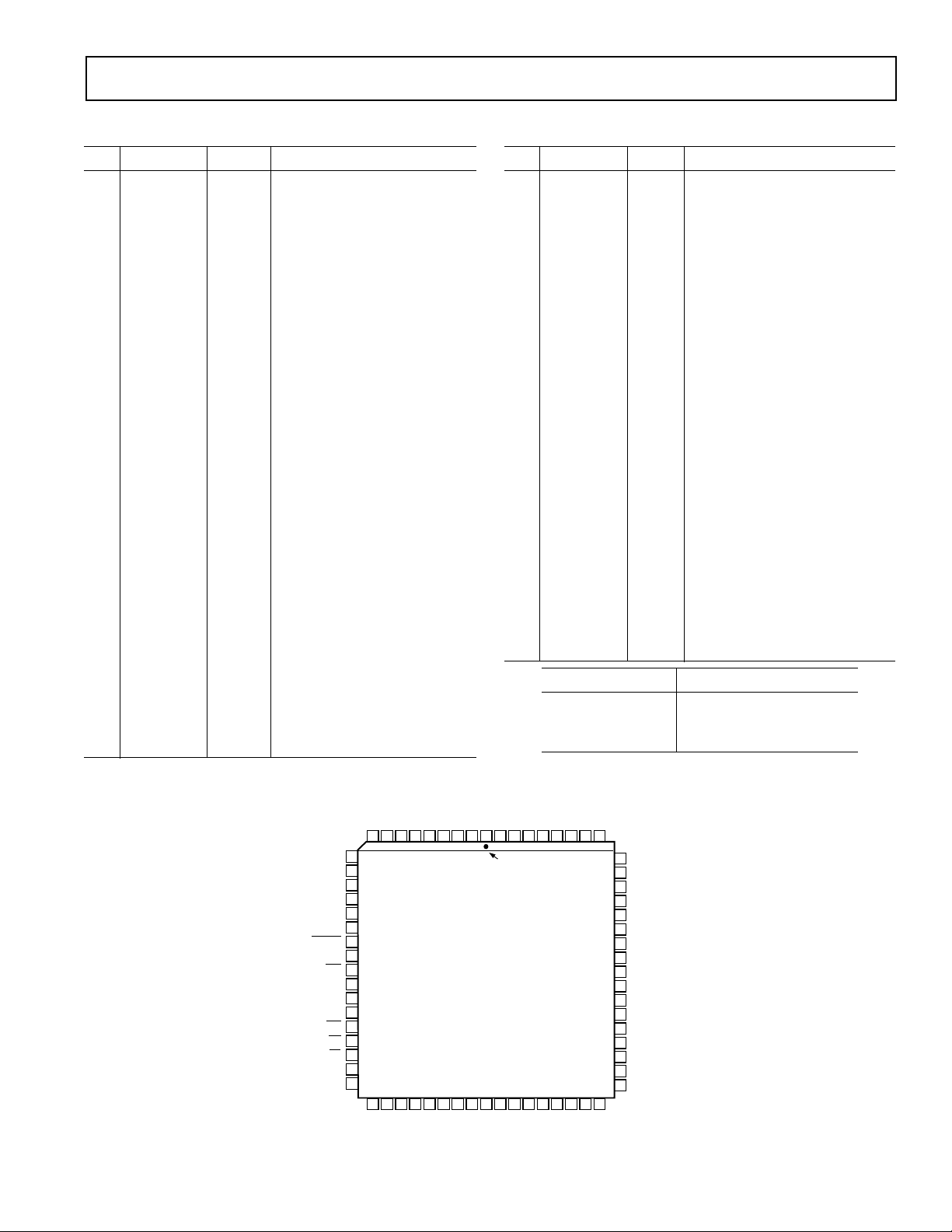
PIN CONFIGURATION
PIO3
PIO5
PIO2
PIO4
9618765 686766656463624321
PIO1
PIO0
D11
D10
D9
ADMC201
TOP VIEW
(Not to Scale)
27 4328 29 30 31 32 33 34 35 36 37 38 39 40 41 42
U
V
AGND
W
AGND
SGND
AUX3
REFIN
AUX2
D7
D8
PIN 1
IDENTIFIER
AUX0
AUX1
D5
D6
DD
V
REFOUT
D4
DGND
D3
DGND
–5–
D2
D1
DGND
DGND
60
D0
59
V
58
DGND
57
DGND
56
DGND
55
A
54
AP
53
B
52
NC
51
BP
50
C
49
CP
48
PWMSYNC
47
STOP
46
DGND
45
NC
44
V
DD
DD
Page 6

ADMC201
ANALOG INPUT BLOCK
The ADMC201 contains an 11-bit resolution, successive approximation analog-to-digital (A/D) converter with twos complement
output data format. The analog input range is ±2.5 V (0 V–5 V)
with a 2.5 V offset as defined by REFIN. The on-chip 2.5 V ±
5% reference is utilized by connecting the REFOUT pin to the
REFIN pin.
The input stage to the A/D converter is a four channel SHA
which allows the four channels (U, V, W and AUX) to be held
simultaneously and then sequentially digitized. The auxiliary
input (AUX) is fed by a four channel multiplexer that allows the
channels AUX0, AUX1, AUX2 and AUX3 to be individually
converted along with the primary channels U, V and W. The
auxiliary inputs are ideal for reading slower changing variables
such as bus voltage and temperature. The A/D conversion time
is determined by the system clock frequency, which can range
from 6.25 MHz to 12.5 MHz. The Sample and Hold (SHA)
acquisition time is 20 system clock cycles and is independent of
the number of channels sampled and/or digitized. Forty system
clock cycles are required to complete each A/D conversion. The
analog channel sampling is flexible and is programmable
through the SYSCTRL register. The minimum number of
channels per conversion is two. The throughput time of the
analog acquisition block can be calculated as follows:
tAA= t
SHA
+ (n × t
CONV
)
where
t
= analog acquisition time,
AA
n = # channels,
= SHA acquisition time (20 × system clock period),
t
SHA
t
= conversion time (40 × system clock period) per channel.
CONV
A/D Conversions are initiated via the CONVST pin. A synchronizing pulse (PWMSYNC) is provided at the beginning of
each PWM cycle. This pulse can be used to synchronize the
A/D conversion process to the PWM switching frequency.
Operating the A/D Converter
The A/D converter can be set up to convert a sequence of channels
as defined in the SYSCTRL register (see Table VI). The default
channel select mode after RESET is to convert channels V and
W only. This is two-/three-phase mode. Three-/three-phase
mode converts channels U, V, W, and/or AUX. Three-/threephase mode is selected by writing a 1 to Bit 3 of the SYSCTRL
register. After the conversion process is complete, the channels
can be read in any order.
There are two methods that can be used to indicate when the
A/D conversions are completed and the data is ready: interrupt
driven and software timing.
Interrupt Driven Method
Interrupts can be used to indicate the end of conversion for a
group of channels. Before beginning any A/D conversions, Bit 7
of the SYSCTRL register must be set to 1 to enable A/D conversion interrupts. Then, when an A/D conversion is complete,
an interrupt will be generated. After an interrupt is detected,
Bit 0 of the SYSSTAT register must be checked to determine if
the A/D converter was the source. Reading the SYSSTAT register automatically clears the interrupt flag bits.
Software Timing Method
An alternative method is to use the DSP or microcontroller to
keep track of the amount of time elapsed between CONVST
and the expected completion time (n × t
CONV
).
Reading Results
The 11-bit A/D conversion results for channels U, V, W and
AUX are stored in the ADCU, ADCV, ADCW and ADCAUX
registers respectively. The twos complement data is left justified
and the LSB is set to zero. The relationship between input voltage and output coding is shown in Figure 5.
011111111110
000000000000
100000000000
OUTPUT
CODE
0V
FULL-SCALE
TRANSITION
FS = 5V
LSB =
2.5
INPUT VOLTAGE
5V
2048
5V–1LSB
Figure 5. Transfer Function
Sample and Hold
After powering up the ADMC201, bring the RESET pin low for
a minimum of two clock cycles in order to enable A/D conversions.
Before initiating the first conversion (CONVST) after a reset,
the SHA time of 20 system clock cycles must occur. A conversion
is initiated by bringing CONVST high for a minimum of one
system clock cycle. The SHA goes into hold mode at the falling
edge of clock.
Following completion of the A/D conversion process, a minimum
of 20 system clock cycles are required before initiating another
conversion in order to allow the sample and hold circuitry to
reacquire the input signals.
If a CONVST is initiated before the 20 clock cycles have elapsed,
the embedded control sequencer will delay conversion until this
requirement is met.
–6–
REV. B
Page 7

ADMC201
PWM TIMER BLOCK OVERVIEW
The PWM timers have 12-bit resolution and support programmable pulse deletion and deadtime. The ADMC201 generates
three center-based signals A, B and C based upon user-supplied
duty cycles values. The three signals are then complemented
and adjusted for programmable deadtime to produce the six
outputs. The ADMC201 PWM master switching frequency can
range from 2.5 kHz to 20 kHz, when using a 10 MHz system
clock. The master frequency selection is set as a fraction of the
PWMTM register. If the system clock is 10 MHz, then the
minimum edge resolution available is 100 ns.
The output format of the PWM block is active LO. There is an
external input to the PWM timers (STOP) that will disable all
six outputs within one system clock when the input is HIGH.
The ADMC201 has a PWM Synchronization output
(PWMSYNC) which brings out the master switching frequency
from the PWM timers. The width of the PWMSYNC pulse is
equal to one system clock cycle. For example, if the system clock
is 10 MHz, the PWMSYNC width would be equal to 100 ns.
PWM Master Switching Period Selection
The switching time is set by the PWMTM register which should
be loaded with a value equal to the system clock frequency
divided by the desired master switching frequency. For example, if the desired switching frequency is 8 kHz and the
system clock frequency is 10 MHz, then the PWMTM register
should be loaded with 1250 (10 MHz/8 kHz). The PWMCHA,
PWMCHB and PWMCHC registers are loaded with the
desired on-time and their values would be calculated as a ratio
of the PWMTM register value. Note: Desired Pulse Density =
(PWMCHx register)/( PWMTM register).
The beginning of each PWM cycle is marked by the PWMSYNC
signal. New values of PWMCHA, PWMCHB and PWMCHC
must all be loaded into their respective registers at least four system clock cycles before the beginning of a new PWM cycle. All
three registers must be updated for any of them to take effect.
New PWM on/off times are calculated during these four clock
cycles and therefore the PWMCHA, PWMCHB and PWMCHC
registers must be loaded before this time. If this timing requirement is not met, then the PWM outputs may be invalid during
the next PWM cycle.
PWM Example
The following example uses a system clock speed of 10 MHz.
The desired PWM master switching frequency is 8 kHz and the
desired on-time for the timers A, B and C are 25%, 50% and
10% respectively. The values for the PWMCHA, PWMCHB
and PWMCHC registers must be calculated as ratios of the
PWMTM register (1250 in this example). To achieve these
duty cycles, load the PWMCHA register with 313 (1250 ×
0.25), PWMCHB with 625 (1250 × 0.5) and PWMCHC with
125 (1250 × 0.1).
Programmable Deadtime
With perfectly complemented PWM drive signals and nonideal
switching characteristics of the power devices, both transistors
in a particular leg might be switched on at the same time, resulting in either a power supply trip, inverter trip or device
destruction. In order to prevent this, a delay must be introduced between the complemented signal edges. For example,
the rising edge of AP occurs before the falling edge of A, and the
falling edge of the complemented A occurs after the rising edge
of A. This capability is known as programmable deadtime.
The ADMC201 programmable deadtime value is loaded into
the 7-bit PWMDT register, in which the LSB is set to zero internally, which means the deadtime value is always divisible by
two. With a 10 MHz system clock, the 0–126 range of values in
PWMDT yield a range of deadtime values from 0 µs to 12.6 µs
in 200 ns steps. Figure 6 shows PWM timer A with a programmable deadtime of PWMDT.
PWMTM
PWMCHA - PWMDT
A
AP
PWMCHA + PWMDT
Figure 6. Programmable Deadtime Example
Pulse Deletion
The pulse deletion feature prevents a pulse from being generated when the user-specified duty cycle results in a pulse
duration shorter than the user-specified deletion value. The
pulse deletion value is loaded into the 7-bit register PWMPD.
When the user-specified on-time for a channel would result in a
calculated pulse width less than the value specified in the
PWMPD register, then the PWM outputs for that channel
would be set to full off (0%) and its prime to full on (100%).
This is valid for A, AP, B, BP, C and CP. This feature would
be used in an environment where the inverter’s power transistors have a minimum switching time. If the user-specified duty
cycle would result in a pulse duration shorter than the minimum
switching time of the transistors, then pulse deletion should be
used to prevent this occurrence. With a 10 MHz system clock,
the 0–127 range of values in PWMPD yield a range of deadtime
values from 0 µs to 12.7 µs in 100 ns steps.
External PWM Shutdown
There is an external input pin (STOP) to the PWM timers that
will disable all six outputs when it goes HIGH. When the STOP
pin goes HIGH, the PWM timer outputs will all go HIGH
within one system clock cycle. When the STOP pin goes LOW,
the PWM timer outputs are re-enabled within one system clock
cycle. If external PWM shutdown isn't required, tie the STOP
pin LOW.
REV. B
–7–
Page 8

ADMC201
VECTOR TRANSFORMATION BLOCK OVERVIEW
The Vector Transformation Block performs both Park and
Clarke coordinate transformations to control a three-phase
motor (Permanent Magnet Synchronous Motor or Induction
Motor) via independent control of the decoupled rotor torque
and flux currents. The Park & Clarke transformations combine
to convert three-phase stator current signals into two orthogonal
rotor referenced current signals Id and Iq. Id represents the flux
or magnetic field current and Iq represents the torque generating current. The Id and Iq current signals are used by the
processor’s motor torque control algorithm to calculate the required direct Vd and quadrature Vq voltage components for the
motor. The forward Park and Clarke transformations are used
to convert the Vd and Vq voltage signals in the rotor reference
frame to three-phase voltage signals (U, V, W) in the stator reference frame. These are then scaled by the processor and
written to the ADMC201’s PWM registers in order to drive the
inverter. The figures below illustrate the Clarke and Park
Transformations respectively.
I
y
I
x
120°
I
w
I
120°
I
u
120°
v
Three-Phase Equivalent
Stator Currents Two-Phase Currents
Figure 7. Reverse Clarke Transformation
I
y
I
x
ρ
90°
I
q
ROTOR
REFERENCE
FRAME AXIS
I
d
Rotating Stationary
Reference Frame Reference Frame
Figure 8. Reverse Park Transformation
V
q
V
d
ρ
90°
V
y
V
x
Stationary Rotating
Reference Frame Reference Frame
Figure 9. Forward Park Transformation
V
y
V
x
120°
W
120°
U
V
120°
Equivalent Three-Phase Stator
Two-Phase Voltage Voltage
Figure 10. Forward Clarke Transformation
Operating/Using the Vector Transformation Block
After powering up the ADMC201, RESET must be driven
low for a minimum of two clock cycles to enable vector
transformations.
The vector transformation block can perform either a forward or
reverse transformation.
Reverse Transformation is defined by the following operations:
(a) Clarke: 3-phase current signals to 2-phase current signals
followed by (b) Park: 2-phase current signals cross multiplied by
sin ρ, cos ρ which effectively measures the current components
with respect to the rotor (stationary) where ρ is the electrical
angle of the rotor field with respect to the stator windings.
Forward transformation is defined by the following operations:
(a) Park: 2-phase voltage signals cross multiplied by sin ρ, cos ρ fol-
lowed by (b) Clarke: 2-phase to 3-phase voltage signal conversion.
In order to provide maximum flexibility in the target system, the
ADMC201 operates in an asynchronous manner. This means
that the functional blocks (analog input, reverse transformation,
forward transformation and PWM timers) operate independently of each other. The reverse and forward vector
transformation operations cannot occur simultaneously. All
vector transformation registers, except for RHO/RHOP, are
twos complement. RHO/RHOP are unsigned ratios of 360°.
For example, 45° would be 45/360 × 2
12
.
Performing a Reverse Transformation
A reverse transformation is initiated by writing to the reverse
rotation angle register RHO and operates on the values in the
PHIP1, PHIP2 and PHIP3 registers. When the reverse transformation is in 2/3 mode, PHIP1 is calculated from PHIP2 and
PHIP3. This is used in systems where only two-phase currents
are measured. The reverse transformation 2/3 mode is set by
clearing Bit 10 in the SYSCTRL register and is the default
mode after RESET.
In order to perform a reverse transformation, first write to the
PHIP2 and PHIP3 registers, and to the PHIP1 register if not in
2/3 mode. Then initiate the transformation by writing the reverse rotation angle to the RHO register.
The reverse rotation will be completed in 37 system clock cycles
after the rotation is initiated. If Bit 6 of the system control register is set, then an interrupt will be generated on completion.
When an interrupt occurs, the user must check Bit 1 of the
SYSSTAT register to determine if the vector transformation
block was the source of the interrupt.
During the vector transformation, the vector transformation
registers must not be written to or the vector rotation results will
be invalid.
–8–
REV. B
Page 9

ADMC201
3
Reverse Clarke Transformation
The first operation is the Clarke transformation in which the
three-phase motor current signals (I
sine and cosine orthogonal signals (I
, Iv, Iw) are converted to
u
and Iy). These signals
x
represent the equivalent currents in a two-phase ac machine and
is the signal format required for the Park rotation. The threephase input signals are of the form:
PHIP1 I
PHIP2 I
PHIP3 I
and the Park rotation requires inputs in the form I
I
sin θ, therefore we need to generate Is sin θ.
s
= Is cos θ
u
= Is cos (θ + 120)
v
= Is cos (θ + 240)
w
cos θ and
s
This is calculated from:
IY I
sin θ =
s
After the reverse transform, registers I
1
(Is cos (θ + 240) – Is cos (θ +120))
and I
contain the 2-
x
y
phase input current information.
In the case where 2- of 3-phase information (PHIP2/3 only) is
provided, then PHIP1 will be derived from the simple fact that
all sum to zero. This value is then placed in the IX register.
IX = I
= Is cos θ = – Is cos (θ + 120) – Is cos (θ + 240)
x
Reverse Park Rotation
IX/IY are then processed together with the digital angle ρ
(RHO) by a Park rotation. If the input signals are I
and Iy,
x
then the rotation can be described by:
ID I
IQ I
= Ix × cos ρ + Iy × sin ρ
d
= –Iy × sin ρ + Iy x cos ρ
q
where ID and IQ are the outputs of the Park rotation.
Cos ρ and sin ρ are required for the Park rotation, and are calculated internally.
Substituting for I
ID I
IQ I
Performing a Forward Transformation
= Is cos θ × cos ρ + Is sin θ × sin ρ = Is cos (θ – ρ)
d
= Is sin θ × cos ρ – Is cos θ × sin ρ = Is sin (θ – ρ)
q
and Iy in the above yields:
x
In order to perform a forward rotation, write values to the VD
and VQ registers and then initiate the transformation by writing
the rotation angle to the register RHOP. The forward transformation will only operate correctly when Bit 10 in the SYSCTRL
register is set (i.e., in 3/3 mode).
The forward rotation will be completed in 40 system clock
cycles after the rotation is initiated. If Bit 6 of the system
control register is set, then an interrupt will be generated on
completion. When an interrupt occurs, the user must check Bit
1 of the system status register, SYSSTAT, to determine if the
vector transformation block was the source of the interrupt.
During the vector transformation, the transformation registers
must not be written to or the vector rotation results will be invalid.
Forward Park Rotation
If the input signals are represented by Vd and Vq, then the
transformation can be described by:
VX V
VY V
where V
= Vd × cos ρ – V
x
= Vd × sin ρ + Vq × cos ρ
y
and Vy are the outputs of the Park Rotation, and are
x
×
sin ρ
q
the inputs to the reverse Clarke transformation.
Forward Clarke Transformation (2- to 3-Phase)
The second operation to be applied to the above results, is the
Forward Clarke Transformation where 2-phase (stator) voltage
signals are converted to 3-phase (stator) voltage signals.
For the inverse Clarke transform we require three-phase outputs
of the form below:
PHV1 V cos α
PHV2 V cos (α + 120)
PHV3 V cos (α + 240)
We have two quadrature voltages (V cos α and V sin α) available.
PHV2 V cos (α + 120) =
PHV3 V cos (α + 240) =
PROGRAMMABLE DIGITAL INPUT/OUTPUT PORT
1
–
× Vcosα –
2
1
–
× V cosα+
2
3
× V sin α
2
3
× V sin α
2
The ADMC201 has a six bit programmable digital I/O port.
Each bit is individually configurable as input or output. All bits
configured as inputs have the ability to operate as interrupt
sources. Each pin is independently capable of generating an interrupt should its input level change.
Configuring the Programmable Digital I/O Port
The PIOCTRL register is used to configure the individual bits
on the programmable digital I/O port as either inputs or outputs
and to enable change of state interrupts. The lower six bits of
PIOCTRL control the direction (either input or output) of the
individual bits. A zero configures the corresponding bit as an
input; conversely a 1 configures the corresponding bit as an output. The upper six bits of PIOCTRL are used to enable the
individual bits for use as change of state interrupt sources. A 0
disables change of state interrupt generation and a 1 enables
change of state interrupt generation. The interrupt enable for a
bit configured as an output is ignored. At power-up or RESET,
all six bits of the digital port are configured as input and change
of state interrupt generation is disabled.
Using the Programmable Digital I/O Port
The PIODATA register is used to write to and read from the
digital I/O port. Bits 0–5 of the PIODATA register correspond
to PIO 0–5 on the ADMC201. Bits 6–11 of PIODATA are unused and always contain 0. Read from PIODATA to determine
the state of PIO 0–5. Write to PIODATA to change the states
of PIO 0–5. Writing to bits configured as input has no effect.
Reading from bits configured as output will return the last value
written.
REV. B
–9–
Page 10

ADMC201
INTERRUPT GENERATION
There are three interrupt sources on the ADMC201 that may be
independently enabled to generate interrupts. The first interrupt source is the Analog Input Block, which, if enabled,
generates an interrupt at the end of conversion. The second interrupt source is the Vector Transformation Block, which, if
enabled, generates an interrupt at the end of a Vector Transformation. The third interrupt source is the Digital I/O Block.
Each digital I/O bit, if configured for input and enabled, generates an interrupt when its input level changes.
When a 1 is stored in Bit 7 of the SYSCTRL register, ADC interrupts are enabled. When a 1 is stored in Bit 6 of the
SYSCTRL register, Vector Transformation interrupts are enabled. When a 1 is stored in any of Bits 6–11 of the PIOCTRL
register, digital I/O change of state interrupts are enabled for
Bits 0–5 respectively. Upon a reset of the chip, all bits are set to
the default condition, 0, thus disabling all interrupts.
When an enabled interrupt occurs, Bit 11 of the SYSSTAT register becomes a 1. If that interrupt had been an ADC interrupt,
Bit 0 of SYSSTAT register would also be set to 1. If that interrupt had been a Vector Transformation interrupt, Bit 1 of
SYSSTAT would be set to 1. If that interrupt had been a digital I/O interrupt, then Bit 2 of the SYSSTAT would be set to 1.
Whenever the SYSSTAT register is read, these four bits go back
to their default state, 0, immediately after their values are loaded
onto the data bus. Upon a reset, these four bits also go to their
default state, 0.
The IRQ pin has an open-drain driver, which will drive it low at
the appropriate times, but the user must supply an external pullup resistor to bring the node back high when it is not being
pulled low.
The IRQ pin operates in one of two modes, edge mode or level
mode. In edge mode, when an enabled interrupt occurs, the
IRQ pin will be driven low for one system clock period. In level
mode, when an enable interrupt occurs, the IRQ pin will be
driven low, and will remain low until the SYSSTAT register is
read. The combination of level mode and the open-drain driver
allows multiple interrupt sources in an application to drive a
single interrupt input line on the host DSP or microprocessor.
Edge mode or level mode is determined with Bit 8 of the
SYSCTRL register. Edge mode (0) is the default; a 1 in this bit
will put the IRQ pin into level mode.
The recommended method of using the interrupt generation capability is to set edge or level mode, enable the appropriate
interrupts, and then monitor the IRQ line. After the IRQ pin
goes low, the SYSSTAT register of the ADMC201 should be
read, (1) to determine if it was this chip that caused the interrupt, if other lines are wired together with this IRQ pin, and
(2) if it was this chip, to determine if it was generated by the
Analog Input, Digital I/O and/or the Vector Transformation
Blocks. Once this is done, the appropriate interrupt handling
routine may be executed.
APPLICATION NOTE LIST
1. AN-407 AC Motor Control Experiments Using the ADMC200
Evaluation Board
2. AN-408 AC Motor Control Using the ADMC200 Motion
Coprocessor
3. AN-409 Advanced Motor Control Techniques Using the
ADMC200 Motion Coprocessor
POWER SUPPLY CONNECTIONS AND SETUP
The nominal positive power supply level (VDD) is +5 V ± 5%.
The Positive Power supply V
ADMC201 V
pins (10, 19, 26, 39, 44, 59). The SGND pin
DD
should be connected to all
DD
(32) and both AGND pins (27, 28) should be star point connected at a point close to the AGND pins of the ADMC201.
The DGND pins (20, 40, 41, 42, 43, 46, 56, 57, 58) should
also be connected to AGND pins close to the ADMC201.
Power supplies should be decoupled at the power pins using a
0.1 µF capacitor. A 220 nF capacitor must also be connected as
close as possible between REFIN (Pin 33) and SGND (Pin 32).
In addition, the IRQ requires a 15K pull-up to the V
supply.
DD
SYSTEM CLOCK FREQUENCY
The nominal range of the input clock for the ADMC201 is
6.25 MHz to 25 MHz. The external CLK frequency can be internally divided down by 2 by writing to Bit 5 of the SYSCTRL
register. If the external CLK is faster than 12.5 MHz then it is
necessary to internally divide it down.
DSP/CONTROLLER INTERFACE
The ADMC201 has a 12-bit bidirectional parallel port for interfacing with Analog Devices’ ADSP-2100 DSP family or
microcontrollers/microprocessors.
The ADMC201 coprocessor is designed to be conveniently interfaced to the ADI’s family of Fixed-Point DSPs. Figures 11
and 12 show the interfacing between the ADMC201 and the
ADSP-2101/2105/2115, ADSP-2171, ADSP-2181, TMS320C2x
DSPs. In the case of the TMS320C2x, some glue logic is required to decode the RD/WR lines and invert the CLKOUT1
signal.
The ADSP-2101/2105/2115 CLKOUT frequency equals the
crystal/clock frequency of its CLKIN. This signal (CLKOUT)
can be used to directly drive the CLK line (Pin 21) on the
ADMC201. The ADMC201 coprocessor can be operated with
a clock frequency between the of 6.25 MHz and 25 MHz. If the
clock frequencies is greater than 12.5 MHz, then it is necessary
to internally divide down the external clock to derive the
ADMC201’s system clock (via SYSCTRL register).
ADDRESS BUS
V
DD
CS
IRQ
RD
WR
CLK
A0–A3
ADMC201
D0–D11*
A0–A13
ADSP-2101/
ADSP-2105/
ADSP-2115–20MHz
ADSP-2171–10MHz
ADSP-2181–10MHz
D0–D23
*NOTE:
BY MAPPING THE ADMC201 DATA BUS TO THE TWELVE HIGHEST BITS
OF THE ADSP DATA BUS, FULL-SCALE OUTPUTS FROM THE ADC
CAN BE REPRESENTED BY ⴞ 1.0 IN FIXED POINT ARITHMETIC.
DMS
IRQ2
CLKOUT
RD
WR
ADDRESS
DECODE
EN
DATA BUS
Figure 11. ADI Digital Signal Processor/Microcomputer
–10–
REV. B
Page 11

ADMC201
ADDRESS BUS
V
DD
A0–A15
TMS320C20
TMS320C25
TMS320C25-50
D0–D15
INTn
STRB
R/W
CLKOUT1
ADDRESS
DECODE
EN
IS
DATA BUS
CS
IRQ
RD
WR
CLK
A0–A3
ADMC201
D0–D11
Figure 12. TI Second Generation Devices TMS320C20/
C25/C25–50
In the case of the ADSP-2171/2181, the system clock is internally scaled, a 10 MHz system clock will derive a 20 MHz
CLKOUT. In the case of the TMS320C2X, the CLKOUT1
signal is derived from the system clock divided by a factor of 4,
consequently a 50 MHz TMS320C25-50 will derive a
12.5 MHz CLKOUT1 for use by the ADMC201.
Note: a pull-up resistor is required on the IRQ (Pin 18) output
from the ADMC201. The STOP (Pin 47) must be tied low if
not in use.
REGISTER ADDRESSING
Four address lines (A0 through A3) are used in conjunction
with the control lines (CS, WR, RD,) to select registers 0
through 15. The CS and RD control lines are active low. The
registers are given symbolic names.
Table II.
Pin Function
CS Enables the ADMC201 register interface
(connect via chip select logic-active low)
RD Places data from the internal register onto the
data bus
WR Loads the internal register with data on the
data bus on its positive edge
DESCRIPTION OF THE REGISTERS
All unspecified register locations are reserved.
SYSCTRL System Control Register (See Tables V,
VI, VII).
SYSSTAT System Status Register (See Table VII).
ADCU These registers contain the results from
ADCV the first three analog input channels
ADCW U, V, and W. The output data format
is twos complement and, therefore, Bit 0
is always zero as the A/D converter
has 11-bit resolution.
ADCAUX This register contains the conversion result
of the auxiliary channels AUX0, AUX1,
AUX2 or AUX3.
PWMTM PWM Master Switching Period
PWMCHA PWM Channel A On-Time
PWMCHB PWM Channel B On-Time
PWMCHC PWM Channel C On-Time
PWMDT PWM Programmable Deadtime Value
PWMPD PWM Programmable Pulse Deletion Value
ID/IQ These are the results of the reverse
rotation (torque and flux components).
PHV1/2/3 These are the results from the forward
Clarke Transformation.
PHIP1/2/3 The inputs for reverse vector transforma-
tion (Clarke and Park).
IX/IY These registers contain the results
of the Clarke transformation that
are the inputs to the reverse Park rotation.
VX, VY VX, VY contain the results of the forward
Park rotation.
RHOP RHOP is the angle used during the
forward vector transformation. Writing to
the RHOP register causes the forward
rotation to start based on values in
RHOP, VD and VQ registers.
RHO RHO is the angle used during the reverse
vector transformation. Writing to this
register starts the reverse rotation using
the values in the RHO, PHIP1/2/3
registers.
RHO and RHOP are unsigned ratios of
360°. For example, 45 degrees would be
45/360 × 2
12
.
PIODATA Write to this register to change the
digital outputs and read from it to
determine the state of digital inputs.
PIOCTRL This register is used to configure the
digital I/O as input or output and to
enable interrupt on change of state.
REV. B
–11–
Page 12

ADMC201
Table III. Write Registers
Name A3A2A1A
Register Function
0
RHO 0000 Load RHO (ρ) and Start Reverse Transform
PHIP1/VD 0001 Reverse Rotation Direct Input/Forward Direct Input
PHIP2/VQ 0010 Reverse Rotation Direct Input/Forward Direct Input
PHIP3 0011 Reverse Rotation Direct Input
RHOP 0100 Load RHOP (ρ) and Start Forward Transform
PWMTM 0101 PWM Master Switching Period
PWMCHA 0110 PWM Channel A On-Time
PWMCHB 0111 PWM Channel B On-Time
PWMCHC 1000 PWM Channel C On-Time
PWMDT 1001 PWM Programmable Deadtime (7-Bit Register)
PWMPD 1010 PWM Pulse Deletion Value (7-Bit Register)
PIOCTRL 1011 Digital I/O Control
PIODATA 1100 Digital I/O Data Write (6-Bit Register)
SYSCTRL 1101 System Control
1110 Reserved
1111 Reserved
Table IV. Read Registers
Name A3A2A1A
ID/PHV1/VX 0000 Reverse Rotation Result (I
IQ/PHV2 0001 Reverse Rotation Result (I
Register Function
0
)/Forward Result Cos +0°
DS
)/Forward Cos +120°
QS
IX/PHV3 0010 Reverse Clarke Cos +0°/Forward Result Cos +240°
IY/VY 0011 Reverse Clarke Cos +90°/Forward Cos +90°
0100 Reserved
ADCV 0101 A/D Conversion Result Channel V
ADCW 0110 A/D Conversion Result Channel W
ADCAUX 0111 A/D Conversion Result Auxiliary Channel
ADCU 1000 A/D Conversion Result Channel U
1001 Reserved
1010 Reserved
1011 Reserved
PIODATA 1100 Digital I/O Data Read (6-Bit Register)
SYSCTRL 1101 System Control
SYSSTAT 1110 System Status
1111 Reserved
–12–
REV. B
Page 13

ADMC201
Table V. System Control (SYSCTRL) Registers
RESET
Bit Function Default
0 Auxiliary Channel Selection 0
1 Auxiliary Channel Selection 0
3 Enables U Channel Conversion
(1 = Enable) Two-/Three-Phase Mode 0
4 Enables AUX Channel Conversion
(0 = Disable, 1 = Enable) 0
5 Divide External Clock by 2
(0 = No, 1 = Yes) 0
6 Park Interrupt Enable 0
7 ADC Interrupt Enable
(0 = Disable, 1 = Enable) 0
8 IRQ Pin Format (Edge or Level Based
Interrupt Requests) (0 = Edge) 0
10 Reverse Rotation (0 = 2/3, 1 = 3/3) 0
Forward Rotation (1 = Enable)
Table VI. SYSCTRL Auxiliary Channel Selection
Bit 0 Bit 1 Auxiliary Channels Converted
0 0 AUX0
0 1 AUX1
1 0 AUX2
1 1 AUX3
Table VII. SYSCTRL Analog Input Channel Selection
Bit 3 Bit 4 Channels Converted Mode
0 0 V, W (Default) Two-/Three-Phase
0 1 V, W, AUX Two-/Three-Phase
1 0 U, V, W Three-/Three-Phase
1 1 U, V, W, AUX Three-/Three-Phase
Bit 0, 1 Auxiliary Channel Selection.
Bit 3 Channel U Conversion Enable. If Bit 3 is set to 1, then
Channel U will be converted along with V, W and/or
AUX. This bit selects three-/three-phase mode.
Bit 4 Aux Channel Conversion Enable. If Bit 4 is set to
1, then the AUX input will be converted along with
the channels V, W and/or U.
Bit 5 If Bit 5 = 1, then the external clock will be divided by
two to derive the system clock. If the external clock
frequency is greater than 12.5 MHz, then this bit must
be set.
Bit 6 Park Interrupt Enable. This bit allows interrupts to
be generated when the Park rotation is completed.
Bit 7 ADC Interrupt Enable. This bit allows interrupts to
be generated when the analog-to-digital conversion
process is complete.
Bit 8 IRQ Pin Format—Edge or Level Interrupt Selection.
If Bit 8 is set to 0, then an interrupt will cause a
pulse of one system clock to be generated on the
IRQ pin. If Bit 8 is set to 1, then an interrupt
causes the IRQ output to go LOW (logic 0). The IRQ
output pin will remain LOW until the SYSSTAT
register is read.
Bit 10 If Bit 10 is set to 1, then the reverse Park transforma-
tion will be formed in 3/3 mode. For Forward
transformations, this bit must be set to 1.
REV. B
–13–
Page 14

ADMC201
Table VIII. System Status Register (SYSSTAT)
1
RESET
Bit Function Default
0 A/D Conversion
Completion Interrupt
(1 = True) 0
1 Vector Transformation
Completion Interrupt
(1 = True) 0
2 Digital I/O Change of State
Interrupt (1 = True) 0
4 Rotation Results are Valid
(1 = Valid) X
2
11 IRQ Generated from This 0
Device (1 = True)
NOTES
1
Reading this register clears the interrupt status flags Bits 0, 1, 2 and 11.
2
Undefined until the first Vector Transformation has started
Bit 0 A/D Conversion Completion Interrupt. This register
is set to 1 when the A/D conversion process has completed and ADC interrupts have been enabled in the
SYSCTRL register.
Bit 1 Interrupt Status. This register is set to 1 when the
Vector Transformation is completed and the Vector
Transformation completion interrupts have been
enabled.
Bit 4 This bit is set to 1 when the rotation results are valid
reading this.
Bit 11 If any interrupt source on the ADMC201 occurs, then
this bit is set to 1.
Table IX. Programmable Digital I/O Control Register
(PIOCTRL)
RESET
Bit Function Default
0 Programmable Digital I/O Direction
Bit 0 (0 = Input, 1 = Output) 0
1 Programmable Digital I/O Direction
Bit 1 (0 = Input, 1 = Output) 0
2 Programmable Digital I/O Direction
Bit 2 (0 = Input, 1 = Output) 0
3 Programmable Digital I/O Direction
Bit 3 (0 = Input, 1 = Output) 0
4 Programmable Digital I/O Direction
Bit 4 (0 = Input, 1 = Output) 0
5 Programmable Digital I/O Direction
Bit 5 (0 = Input, 1 = Output) 0
6 Programmable Digital I/O Bit 0 Interrupt
(0 = Disable, 1 = Enable) 0
7 Programmable Digital I/O Bit 1 Interrupt
(0 = Disable, 1 = Enable) 0
8 Programmable Digital I/O Bit 2 Interrupt
(0 = Disable, 1 = Enable) 0
9 Programmable Digital I/O Bit 3 Interrupt
(0 = Disable, 1 = Enable) 0
10 Programmable Digital I/O Bit 4 Interrupt
(0 = Disable, 1 = Enable) 0
11 Programmable Digital I/O Bit 5 Interrupt
(0 = Disable, 1 = Enable) 0
Bits 0–5 Sets corresponding Digital I/O bits as either input
or output.
Bits 6–11 Configures Digital I/O Bits 0–5 as interrupt on
change of state sources. Enabling interrupts for bits
configured as output has no effect.
–14–
REV. B
Page 15

OUTLINE DIMENSIONS
Dimensions shown in inches and (mm).
68-Lead Plastic Leaded Chip Carrier
(P-68A)
ADMC201
61
60
44
43
0.175 (4.45)
0.169 (4.29)
0.104 (2.64) TYP
0.050
(1.27)
TYP
0.925 (23.50)
0.895 (22.73)
0.019 (0.48)
0.017 (0.43)
0.029 (0.74)
0.027 (0.69)
PIN 1
IDENTIFIER
BOTTOM VIEW
(PINS UP)
C2072a–1.5–4/00 (rev. B)
0.995 (25.27)
0.985 (25.02)
9
10
(PINS DOWN)
26
27
0.954 (24.23)
0.950 (24.13)
PIN 1
IDENTIFIER
TOP VIEW
SQ
SQ
REV. B
PRINTED IN U.S.A.
–15–
 Loading...