

Page 1
Power Supply and Watchdog Timer
a
FEATURES
Precision Voltage Monitor (4.31 V)
Watchdog Timeout Monitor
Selectable Watchdog Timeout—0.75 ms, 1.5 ms,
12.5 ms, 25 ms
Two RESET Outputs
APPLICATIONS
Microprocessor Systems
Computers
Printers
Controllers
Intelligent Instruments
GENERAL DESCRIPTION
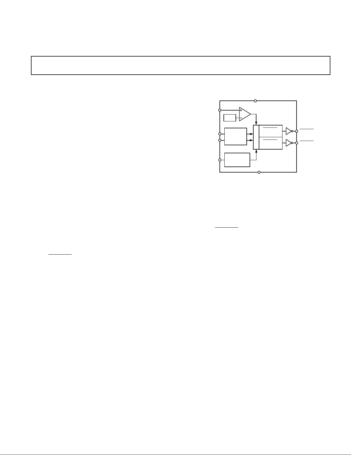
The ADM9690 contains a voltage monitoring comparator and a
watchdog timer monitor. It is designed to monitor the 5 V
power supply to a microprocessor and the microprocessor operation via a watchdog function.
The voltage monitoring comparator monitors the voltage on
V
. If it drops outside tolerance, as will happen during a
MON
power-fail, two reset signals are generated. Both reset signals go
active (low) simultaneously. They will remain active while
is below the threshold, and for 50 ms (RESET(1)) or
V
MON
60 ms (RESET(2)) after V
old. RESET(1) is intended to provide a power-on reset signal
for the µP while RESET(2) is used to hold additional circuitry
in a reset state until the µP has regained control following a
power-up. The voltage monitoring circuitry remains operational
with V
as low as 2 V.
CC
climbs above the reset thresh-
MON
Monitoring Circuit
ADM9690
FUNCTIONAL BLOCK DIAGRAM
V
CC
V
MON
4.31V
OSC SEL1
OSC SEL2
WATCHDOG
INPUT (WDI)
WATCHDOG
TIMEBASE
WATCHDOG
TRANSITION
DETECTOR
The watchdog timer monitoring circuit is designed to monitor
the activity on the WDI input. This input is normally connected
to an output line on the µP. Its function is to check that the
microprocessor has not stalled in an infinite loop. If there is a
period of inactivity for the watchdog timeout period, both reset
outputs are activated. As above, RESET(1) remains low for
50 ms while RESET(2) remains low for an additional 10 ms.
The watchdog timer is restarted when RESET(1) goes inactive.
The actual watchdog timeout period is adjustable using two
select inputs SEL1 and SEL2.
The ADM9690 is available in an 8-lead SOIC package. It is
specified over the industrial temperature range.
GND
ADM9690
RESET(1)
TIMER
RESET(2)
TIMER
RESET(1)
RESET(2)
REV. A
Information furnished by Analog Devices is believed to be accurate and
reliable. However, no responsibility is assumed by Analog Devices for its
use, nor for any infringements of patents or other rights of third parties
which may result from its use. No license is granted by implication or
otherwise under any patent or patent rights of Analog Devices.
One Technology Way, P.O. Box 9106, Norwood, MA 02062-9106, U.S.A.
Tel: 781/329-4700 World Wide Web Site: http://www.analog.com
Fax: 781/326-8703 © Analog Devices, Inc., 2000
Page 2

ADM9690–SPECIFICATIONS
(VCC = Full Operating Range. TA = T
MIN
to T
unless otherwise noted)
MAX
Parameter Min Typ Max Units Test Conditions/Comments
VCC OPERATING VOLTAGE RANGE 4.3 5.5 V
SUPPLY CURRENT 55 100 µA
RESET AND WATCHDOG TIMER
Reset Voltage Threshold 4.2 4.31 4.42 V V
Falling TA = 0°C to +70°C
MON
Reset Threshold Hysteresis 30 mV
Reset Timeout Delay (t1) 50 75 ms Figure 7, 8
RESET(2) Timeout Delay (t2) 10 15 ms Figure 7, 8
WATCHDOG TIMEOUT PERIOD (TWD) 0.4 0.75 1.28 ms SEL2 = 0, SEL1 = 0
1.0 1.5 2.4 ms SEL2 = 0, SEL1 = 1
9.0 12.5 19 ms SEL2 = 1, SEL1 = 0
18 25 38 ms SEL2 = 1, SEL1 = 1
WDI INPUT PULSEWIDTH 100 ns V
RESET(1)/(2) Output Voltage 0.1 0.4 V I
0.3 0.4 V I
0.45 0.7 V I
3.5 V I
= 0.4, VIH = 3.5 V
IL
= 3.2 mA
SINK
= 10 mA,
SINK
= 15 mA,
SINK
SOURCE
WDI INPUT THRESHOLD
Logic Low 0.8 V 150 ns Pulse
Logic High 3.5 V 150 ns Pulse
WDI Input Current 1.2 5 µA WDI = V
–5 –1.2 µA WDI = 0 V
SEL1/2 Input Current –1 +1 µA SEL = V
–10 –5 10 µA SEL = 0 V
Specifications subject to change without notice.
= 1 µA
CC
CC
–2–
REV. A
Page 3

ADM9690
ABSOLUTE MAXIMUM RATINGS*
(TA = +25°C unless otherwise noted)
VCC . . . . . . . . . . . . . . . . . . . . . . . . . . . . . . . . . –0.3 V to +6 V
V
. . . . . . . . . . . . . . . . . . . . . . . . . –0.3 V to V
MON
+ 0.3 V
CC
Input Current
. . . . . . . . . . . . . . . . . . . . . . . . . . . . . . . . . . . . 200 mA
V
CC
GND . . . . . . . . . . . . . . . . . . . . . . . . . . . . . . . . . . . 200 mA
Digital Output Current . . . . . . . . . . . . . . . . . . . . . . . 200 mA
Power Dissipation, R-8 SOIC . . . . . . . . . . . . . . . . . . 400 mW
Thermal Impedance . . . . . . . . . . . . . . . . . . . . . . 120°C/W
θ
JA
Industrial (A Version) . . . . . . . . . . . . . . . . . . –40°C to +85°C
Lead Temperature (Soldering, 10 secs) . . . . . . . . . . . +300°C
Vapor Phase (60 secs) . . . . . . . . . . . . . . . . . . . . . . +215°C
Infrared (15 secs) . . . . . . . . . . . . . . . . . . . . . . . . . . +220°C
Storage Temperature Range . . . . . . . . . . . . –65°C to +150°C
ESD Rating . . . . . . . . . . . . . . . . . . . . . . . . . . . . . . . . . . . 4 kV
*Stresses above those listed under Absolute Maximum Ratings may cause perma-
nent damage to the device. This is a stress rating only; functional operation of the
device at these or any other conditions above those listed in the operational sections
of this specification is not implied. Exposure to absolute maximum ratings for
extended periods of time may affect device reliability.
ORDERING GUIDE
Temperature Package Package
Model Range Description Option
ADM9690AR –40°C to +85°C 8-Lead Narrow SO-8
Body SOIC
PIN CONFIGURATION
PIN FUNCTION DESCRIPTIONS
Mnemonic Function
V
V
CC
MON
Power Supply Input; +5 V.
Voltage Monitoring Input.
GND 0 V. Ground reference for all signals.
RESET(1) Logic Output. RESET(1) goes low if V
MON
falls below the Reset Threshold or the Watch-
dog timer is not serviced within its timeout
period. The reset threshold is typically 4.4 V
for the ADM9690. RESET(1) remains low
for 50 ms after V
returns above the thresh-
CC
old. RESET(1) also goes low for 50 ms if the
Watchdog Timer is not serviced within its
timeout period.
RESET(2) Logic Output. RESET(2) goes low simulta-
neously with RESET(1) but remains low for
an additional 10 ms.
WDI Watchdog Input. If an edge is not detected on
WDI within the selectable watchdog timeout
period, RESET(1) and RESET(2) are forced
low for their respective timeout periods. The
watchdog timer restarts with each positive
or negative going transition on the WDI
line. Following a reset it is restarted when
RESET(1) goes inactive (high). The Watch-
dog Timer may be disabled if WDI is left
floating or is driven to midsupply.
SEL1, 2 Watchdog Timeout selection inputs. Refer to
Table I.
V
MON
GND
SEL1
SEL2
1
2
ADM9690
TOP VIEW
3
(Not to Scale)
4
8
V
7
RESET(1)
6
RESET(2)
5
WDI
CC
–3–REV. A
Page 4

ADM9690
–Typical Performance Curves
100
CH1 1.0V CH2 M 500ms
1.0V
CH1
Figure 1. Reset Output Voltage vs. Supply
4.412
4.410
4.408
4.406
4.404
4.402
4.400
4.398
RESET VOLTAGE THRESHOLD – Volts
4.396
–60 120–30 0 30 60 90
TEMPERATURE – C
380mV
V
CC
RESET
RESET2/TIMEOUT
RESET1/TIMEOUT
WATCHDOG TIMEOUT
PERIOD
WATCHDOG AND RESET TIMEOUT PERIOD – ms
10
2.5 5.53.0 3.5 4.0 4.5 5.0
VCC – Volts
6.0 6.5
Figure 3. Watchdog and Reset Timeout Period vs. Supply
@ –40
°
C
72.0
71.6
71.2
70.8
70.4
70.0
69.6
BATTERY SUPPLY CURRENT – A
69.2
68.8
–60 120–30 0 30 60 90
TEMPERATURE – C
Figure 2. Reset Voltage Threshold vs. Temperature
+5V
V
V
MON
OSC SEL1
OSC SEL2
4.31V
WATCHDOG
TIMEBASE
CC
ADM9690
GND
Figure 5. Typical Application Circuit
RESET(2)
TIMER
RESET(1)
TIMER
WATCHDOG
TRANSITION
DETECTOR
Figure 4. Supply Current vs. Temperature
AUXILIARY
CIRCUITRY
RESET
RESET(2)
RESET(1)
WATCHDOG
INPUT (WDI)
RESET
P
I/O LINE
–4–
REV. A
Page 5

ADM9690
POWER SUPPLY AND WATCHDOG MONITORING
CIRCUIT
The ADM9690 contains a power supply voltage monitoring
comparator and a watchdog timer monitor. Either V
MON
dropping outside tolerance or the watchdog timer timing out results
in a reset sequence as discussed below. Two reset outputs are
provided. RESET(1) and RESET(2).
POWER FAIL/POWER-ON RESET
When V
falls below the reset threshold (4.4 V) both RESET
MON
outputs are forced low immediately.
On power-up, RESET(1) will remain low for 50 milliseconds
after V
rises above the reset threshold. This provides a
MON
power-on reset for the microprocessor. RESET(2) remains
active low for an additional 10 ms. RESET(1) is intended to
V
CC
V
MON
OSC SEL1
OSC SEL2
WATCHDOG
INPUT (WDI)
4.31V
WATCHDOG
TIMEBASE
WATCHDOG
TRANSITION
DETECTOR
GND
ADM9690
RESET(1)
TIMER
RESET(2)
TIMER
RESET(1)
RESET(2)
Figure 6. Functional Block Diagram
provide a power-on reset signal for the µP while RESET(2) is
used to hold additional circuitry in a reset state until the µP has
regained control following a power-up.
The guaranteed minimum and maximum thresholds for the
ADM9690 are 4.3 V and 4.5 V.
Watchdog Timer RESET
The watchdog timer circuit monitors the activity of the microprocessor in order to check that it is not stalled in an infinite
loop. An output line on the processor may be used to toggle the
Watchdog Input (WDI) line. If this line is not toggled within the
selected timeout period, both RESET outputs are taken active
(low). RESET(1) remains low for 50 ms and RESET(2) remains low for an additional 10 ms . Each transition (either
positive-going or negative-going) of WDI after RESET(1) has
gone inactive restarts the watchdog timer. The actual watchdog
timeout period is adjustable using SEL1 and SEL2. Four timeout
periods are selectable. Please refer to Table I.
The watchdog timer is restarted at the end of RESET(1)
(RESET(1) going high), whether the reset was caused by lack of
activity on WDI or by V
falling below the reset threshold.
MON
Table I.
Watchdog Timeout
SEL2 SEL1 Period tWD (ms)
0 0 0.75
0 1 1.5
1 0 12.5
11 25
V
MON
RESET(1)
RESET(2)
Figure 7. Power-On
WDI
t
1
RESET(1)
t
2
RESET(2)
RESET
Timing
Figure 8. Watchdog
t
WD
t
1
t
2
RESET
Timing
–5–REV. A
Page 6

ADM9690
0.1574 (4.00)
0.1497 (3.80)
OUTLINE DIMENSIONS
Dimensions shown in inches and (mm).
8-Lead Narrow Body SOIC
(SO-8)
0.1968 (5.00)
0.1890 (4.80)
8
5
0.2440 (6.20)
41
0.2284 (5.80)
PIN 1
0.0098 (0.25)
0.0040 (0.10)
SEATING
PLANE
0.0500
(1.27)
BSC
0.0688 (1.75)
0.0532 (1.35)
0.0192 (0.49)
0.0138 (0.35)
0.0098 (0.25)
0.0075 (0.19)
0.0196 (0.50)
0.0099 (0.25)
8°
0°
0.0500 (1.27)
0.0160 (0.41)
x 45°
C3135a–1.5–3/00 (rev. A)
–6–
PRINTED IN U.S.A.
REV. A
 Loading...