

Page 1
L
H
V
REF
NC = NO CONNECT
L
H
L
H
L
H
PWROK
MONITOR
LOGIC
14
13
12
11
16
15
10
9
8
1
2
3
4
7
6
5
GND
SU1
SU2
SU3
SU4
NC
ERRX
V
CC
ERR1
ERR2
PWROK
ERR3
ERR4
DIS
ERRY
SU4DET
ADM9264
Quad Power Supply Monitor
a
FEATURES
Monitoring of 12 V, 5 V, 3.3 V and 2.8 V Supplies in
Parallel
Auxiliary Sensor Inputs
Low Power: 25 mA Typical
Internal Comparator Hysteresis
Power Supply Glitch Immunity
from 2.5 V to 6 V
V
CC
Guaranteed from –4 08 C to +858C
No External Components
16-Pin Narrow SOIC Package (150 Mil Wide)
APPLICATIONS
Microprocessor Systems
Computers
Controllers
Intelligent Instruments
Network Systems
GENERAL DESCRIPTION
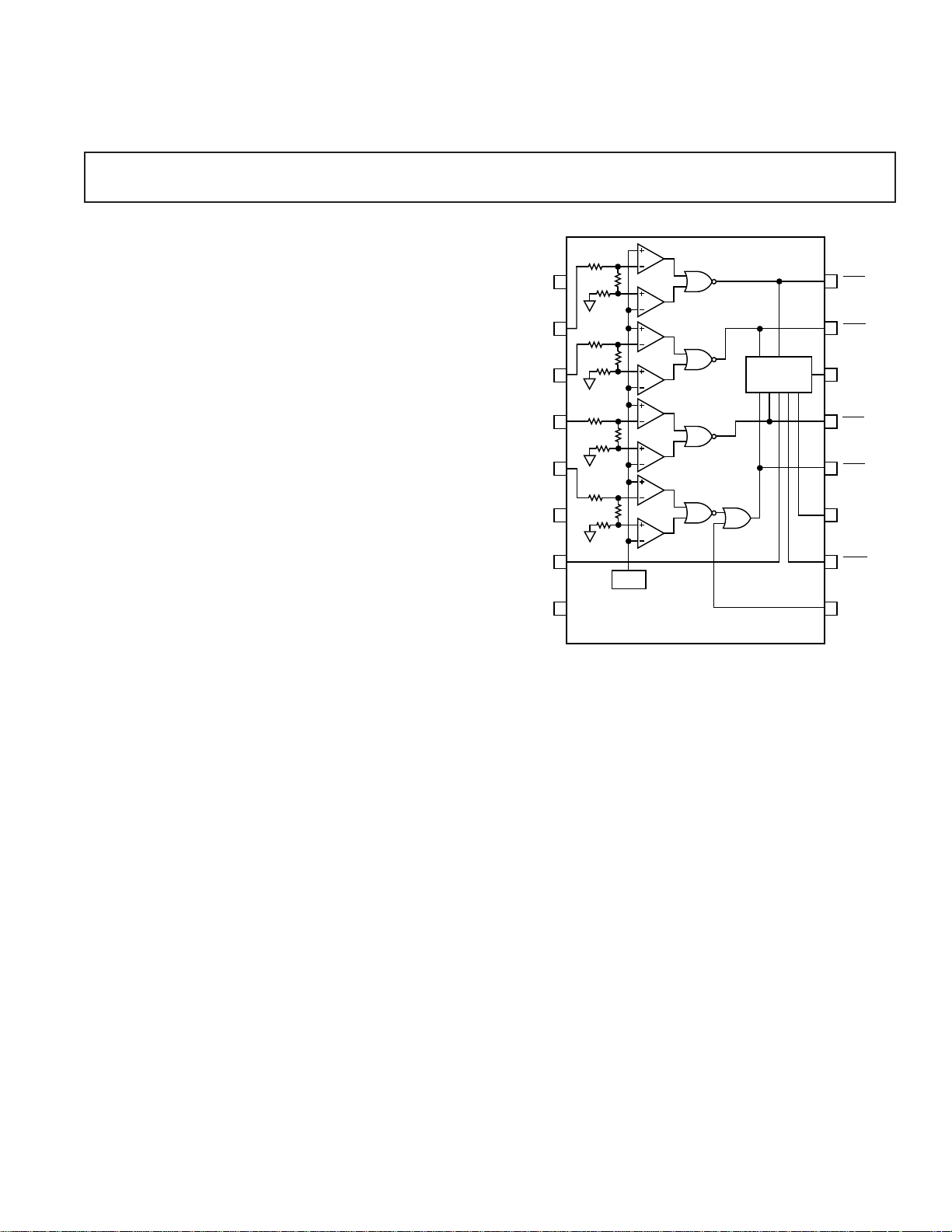
The ADM9264 is a Quad Supply Monitor IC which simultaneously monitors four separate power supply voltages and outputs error signals if any of the supply voltages go out of limits.
It is designed for PC supply monitoring but can be used on
any system where multiple power supplies require monitoring. The error output signals are available individually and also
gated into a common output - PWROK. Auxiliary inputs
ERRX, ERRY are provided which are also gated into the main
PWROK signal. These inputs allow signals from other monitoring circuits (for example temperature sensor, alarm, etc.) to be
linked into the ADM9264.
Each power supply monitor circuit uses a proprietary window
comparator design whereby a three resistor network is used in
conjunction with two comparators and a single precision voltage
reference to check if the supply is within its required operating
tolerance. An added feature of this design is that the power
supply voltages being monitored can be higher than the power
supply voltage to the monitoring IC itself.
for Desktop PCs
ADM9264
FUNCTIONAL BLOCK DIAGRAM
Analog Devices’ experience in the design of power supply supervisory circuits is used to provide an optimum solution for the
overall circuit in terms of cost, performance and power consumption. Key features of the design include the incorporation
of hysteresis and glitch immunity into the comparators, which
minimizes the possibility of spurious triggering by noise spikes
on the supplies being monitored.
The part is manufactured on one of Analog Devices’ proprietary
BiCMOS processes, which also includes high performance thin
film resistors to achieve the accuracy required for the precision
voltage reference and power supply high and low trip points.
REV. 0
Information furnished by Analog Devices is believed to be accurate and
reliable. However, no responsibility is assumed by Analog Devices for its
use, nor for any infringements of patents or other rights of third parties
which may result from its use. No license is granted by implication or
otherwise under any patent or patent rights of Analog Devices.
One Technology Way, P.O. Box 9106, Norwood, MA 02062-9106, U.S.A.
Tel: 617/329-4700 World Wide Web Site: http://www.analog.com
Fax: 617/326-8703 © Analog Devices, Inc., 1997
Page 2

ADM9264–SPECIFICATIONS
(VCC = Full Operating Range, TA = T
MIN
to T
unless otherwise noted)
MAX
Parameter Min Typ Max Units Test Conditions/Comments
OPERATING TEMPERATURE RANGE –40 85 °C Industrial (A Version)
VCC SUPPLY VOLTAGE 2.5 6.0 V
V
SUPPLY CURRENT 25 75 µA Digital Inputs = V
CC
/GND
CC
SU1 INPUT RESISTANCE 200 240 kΩ I IN ~ 50 µA when SU1 = 12 V
SU2 INPUT RESISTANCE 85 100 kΩ I IN ~ 50 µA when SU2 = 5 V
SU3 INPUT RESISTANCE 55 66 kΩ I IN ~ 50 µA when SU3 = 3.3 V
SU4 INPUT RESISTANCE 45 56 kΩ I IN ~ 50 µA when SU4 = 2.8 V
SU1 HIGH TRIP POINT 12.72 12.96 13.2 V Measured with SU1 Rising
SU2 HIGH TRIP POINT 5.35 5.45 5.55 V Measured with SU2 Rising
SU3 HIGH TRIP POINT 3.53 3.60 3.66 V Measured with SU3 Rising
SU4 HIGH TRIP POINT 2.94 3.00 3.05 V Measured with SU4 Rising
SU1 LOW TRIP POINT 10.8 11.04 11.28 V Measured with SU1 Falling
SU2 LOW TRIP POINT 4.45 4.55 4.65 V Measured with SU2 Falling
SU3 LOW TRIP POINT 2.94 3.00 3.07 V Measured with SU3 Falling
SU4 LOW TRIP POINT 2.55 2.60 2.66 V Measured with SU4 Falling
SU1 HYSTERESIS 320 mV Measured at SU1
SU2 HYSTERESIS 130 mV Measured at SU2
SU3 HYSTERESIS 90 mV Measured at SU3
SU4 HYSTERESIS 80 mV Measured at SU4
GLITCH IMMUNITY 10 µs 100 mV Glitch on V
or SU1-4
CC
PROPAGATION DELAY 10 µs Delay from Supply Going Outside
Tolerance until Output Changes
DIGITAL INPUT LOW, V
DIGITAL INPUT HIGH, V
DIGITAL INPUT LOW, V
DIGITAL INPUT HIGH, V
IL
IH
IL
IH
2.4 V 4.0 V < VCC < 6 V
2.0 V 2.5 V < VCC < 4.0 V
0.8 V 4.0 V < VCC < 6 V
0.5 V 2.5 V < VCC < 4.0 V
DIGITAL INPUT CURRENT –1 +1 µA (ERRX, ERRY, DIS)
OPEN DRAIN OUTPUT LOW 0.4 V 10 kΩ External to Positive Supply V+
OPEN DRAIN OUTPUT HIGH V+ –0.25 V 10 kΩ External to Positive Supply V+
SUPPLY RANGE FOR V+ 2.5 6.0 V V+ Can Be Different from V
Specifications subject to change without notice.
CC
–2–
REV. 0
Page 3
ADM9264
WARNING!
ESD SENSITIVE DEVICE
ABSOLUTE MAXIMUM RATINGS*
(T
= +25°C unless otherwise noted)
A
ORDERING GUIDE
VCC . . . . . . . . . . . . . . . . . . . . . . . . . . . . . . . . . –0.3 V to +6 V
SU1, SU2, SU3, SU4 . . . . . . . . . . . . . . . . . . –0.3 V to +15 V
All Other Inputs . . . . . . . . . . . . . . . . . . –0.3 V to V
+ 0.3 V
CC
All Outputs . . . . . . . . . . . . . . . . . . . . . . . . . . . –0.3 V to +6 V
Output Current
ERR1-4, PWROK . . . . . . . . . . . . . . . . 20 mA
Operating Temperature Range
Industrial (A Version) . . . . . . . . . . . . . . . . –40°C to +85°C
Power Dissipation, R-16A . . . . . . . . . . . . . . . . . . . 700 mW
θ
Thermal Impedance . . . . . . . . . . . . . . . . . . . 110°C/W
JA
Lead Temperature (Soldering, 10 secs) . . . . . . . . . . . . +300°C
Model Range Option
ADM9264ARN –40°C to +85°C R-16A
ADM9264ARN-REEL
ADM9264ARN-REEL7
NOTES
1
R = Small Outline IC.
2
2500 devices per reel.
3
1000 devices per reel.
2
3
Vapor Phase (60 secs) . . . . . . . . . . . . . . . . . . . . . . . +215°C
Infrared (15 secs) . . . . . . . . . . . . . . . . . . . . . . . . . . . +220°C
Storage Temperature Range . . . . . . . . . . . . –65°C to +150°C
*Stresses above those listed under Absolute Maximum Ratings may cause perma-
nent damage to the device. This is a stress rating only; functional operation of the
device at these or any other conditions above those listed in the operational sections
of this specification is not implied. Exposure to absolute maximum ratings for
extended periods of time may affect device reliability.
CAUTION
ESD (electrostatic discharge) sensitive device. Electrostatic charges as high as 4000 V readily
accumulate on the human body and test equipment and can discharge without detection.
Although the ADM9264 features proprietary ESD protection circuitry, permanent damage may
occur on devices subjected to high energy electrostatic discharges. Therefore, proper ESD
precautions are recommended to avoid performance degradation or loss of functionality.
Temperature Package
–40°C to +85°C R-16A
–40°C to +85°C R-16A
1
REV. 0
–3–
Page 4
ADM9264
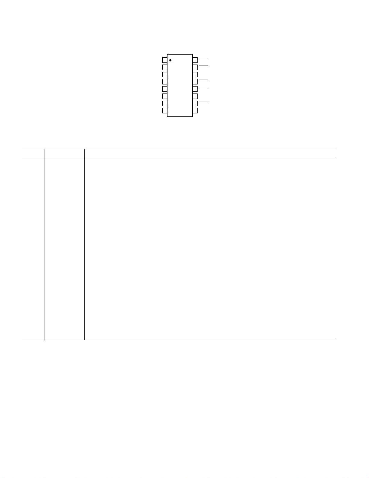
PIN CONFIGURATION
GND
1
SU1
2
SU2
3
SU3
4
SU4
5
NC
6
ERRX
7
V
8
CC
NC = NO CONNECT
ADM9264
TOP VIEW
(Not to Scale)
16
15
14
13
12
11
10
9
ERR1
ERR2
PWROK
ERR3
ERR4
DIS
ERRY
SU4DET
PIN FUNCTION DESCRIPTIONS
Pin No. Mnemonic Function
1 GND Ground.
2 SU1 Supply to Be Monitored. 12 V ± 6%.
3 SU2 Supply to Be Monitored. 5 V ± 7%.
4 SU3 Supply to Be Monitored. 3.3 V ± 7%.
5 SU4 Supply to Be Monitored. 2.8 V ± 5%.
6 NC No Connect.
7 ERRX Digital Input. Auxiliary error input (active high). When High it forces PWROK to be Low.
8V
CC
Supply Monitor IC Power Supply. Can be powered off any power supply between 2.5 V and 6 V
including one of the supplies being monitored (except for SU1).
9 SU4DET Digital Input. Disable SU4. When High it causes ERR4 to pull high through 10 kΩ external resistor to
a positive power supply.
10 ERRY Digital Input. Auxiliary error input (active low). When Low it forces PWROK to be Low.
11 DIS Digital Input. When High it forces PWROK to be High.
12 ERR4 Open Drain Output. Pulls high through 10 kΩ external resistor to a positive power supply when
SU4DET is high or SU4 is within its required tolerance of 2.8 V ± 5%. Pulls Low otherwise.
13 ERR3 Open Drain Output. Low when SU3 is outside its required tolerance of 3.3 V ± 7%. Pulls High other-
wise through 10 kΩ external resistor to a positive power supply.
14 PWROK Open Drain Output. Pulls High through external 10 kΩ resistor to a positive power supply when SU1,
SU2, SU3 and SU4 are all within their required tolerances and when ERRY is High and when ERRX
is Low. Pulls Low otherwise.
15 ERR2 Open Drain Output. Low when SU2 is outside its required tolerance of 5 V ± 7%. Pulls High other-
wise through 10 kΩ external resistor to a positive power supply.
16 ERR1 Open Drain Output. Low when SU1 is outside its required tolerance of 12 V ± 6%. Pulls High other-
wise through 10 kΩ external resistor to a positive power supply.
–4–
REV. 0
Page 5

ADM9264
CIRCUIT INFORMATION
Monitor Inputs SU1 to SU4
The ADM9624 is provided with four analog inputs, SU1 to
SU4, to monitor supply voltages of +12 V, +5 V, +3.3 V and
+2.8 V. Each input is connected to a window comparator consisting of a pair of voltage comparators and a two-input NOR
gate. Each pair of comparators obtains a reference voltage
from a precision internal reference, and each input to be
monitored is connected to the comparators via a precision,
thin film attenuator, whose resistor ratios determine the trip
points of each comparator. As the input voltages are attenuated before reaching the comparators, they may exceed the
supply voltage of the ADM9264 without exceeding the common-mode or differential input range of the comparators.
When the input voltage is within limits, the outputs of both
comparators are low, so the output of the NOR gate is high. If
the voltage on the inverting input of the low comparator falls
below the reference voltage, or the voltage on the noninverting
input of the high comparator rises above the reference voltage,
the output of the NOR gate will go low.
Error Outputs
Error outputs ERR1 to ERR4 are open-drain outputs that are
OFF (high) when the corresponding input voltage is within
limits and ON (low) when the input is out of limit. Each error
output requires a 10 kΩ pull-up resistor to a positive supply,
which may be different from V
if required. The open-drain
CC
construction allows two or more of these outputs to be wireANDed together if required.
Auxiliary Inputs ERRX, ERRY
ERRX and ERRY are TTL-compatible auxiliary inputs that
allow external signals such as temperature alarms to be linked
into the ADM9264. ERRX is active high and forces PWROK
low when it is high. ERRY is active low and forces PWROK low
when it is low.
DIS Input
The disable input, DIS, is a TTL-compatible input. It overrides
all other inputs to the PWROK logic and forces PWROK high
when it is high.
SU4DET Input
SU4DET is a TTL-compatible input that disables the ERR4
output, causing ERR4 to go high when SU4DET is high. This
allows the SU4 input to be disabled easily for systems that do
not have a 2.8 V supply.
PWROK Output
The PWROK output combines the four error outputs and the
auxiliary inputs to give a common “Power OK” output. If the
four error outputs are high, ERRX is low, ERRY is high and
DIS is low then PWROK is high, otherwise PWROK is low.
PWROK is an open-drain output and requires a 10K pull-up
resistor to a positive supply, which may be different from V
CC
if
required. A truth table for the PWROK output is following.
Truth Table
DIS ERRX ERRY ERR4 ERR3 ERR2 ERR1 PWROK
00 1 1111 1
0X X XXX0 0
0XXXX0X0
0XXX0XX0
0XX0XXX0
0X 0 XXXX 0
01 X XXXX 0
1X X XXXX 1
X = don’t care.
Power Supply V
CC
The ADM9264 can be powered from any supply voltage between
2.5 V and 6 V. This includes any of the supply voltages apart
from that connected to SU1, since this is greater than 6 V.
The logic outputs are open-drain and take their output high
level from the voltage connected to the pull-up resistor, so they
are not dependent on the value of V
CC
.
REV. 0
–5–
Page 6

Typical Performance Characteristics–ADM9264
0.5
0.4
0.3
0.2
HYSTERESIS – Volts
0.1
0
–30 85–20
0 15253545556575
TEMPERATURE – °C
Figure 1. Hysteresis vs. Temperature for SU1—Low to High
0.5
0.4
0.3
0.2
HYSTERESIS – Volts
0.1
0.25
0.2
0.15
0.1
HYSTERESIS – Volts
0.05
0
–30 85–20
0 15253545556575
TEMPERATURE – °C
Figure 4. Hysteresis vs. Temperature for SU2—High to Low
0.12
0.1
0.08
0.06
0.04
HYSTERESIS – Volts
0.02
0
–30 85–200 15253545556575
TEMPERATURE – °C
Figure 2. Hysteresis vs. Temperature for SU1—High to Low
0.2
0.15
0.1
HYSTERESIS – Volts
0.05
0
–30 85–20
015253545556575
TEMPERATURE – °C
Figure 3. Hysteresis vs. Temperature for SU2—Low to High
0
–30 85–20
0 15253545556575
TEMPERATURE – °C
Figure 5. Hysteresis vs. Temperature for SU3—Low to High
0.14
0.12
0.1
0.08
0.06
HYSTERESIS – Volts
0.04
0.02
0
–30 85–20
015253545556575
TEMPERATURE – °C
Figure 6. Hysteresis vs. Temperature for SU3—High to Low
–6–
REV. 0
Page 7

ADM9264
60
40
50
0
–10
–20
–30
20
10
30
TEMPERATURE – °C
1000 20406080
–20
TRIP POINT VARIATION – mV
60
40
50
0
–10
–20
–30
20
10
30
TEMPERATURE – °C
1000 20406080
–20
TRIP POINT VARIATION – mV
0.12
0.1
0.08
0.06
0.04
HYSTERESIS – Volts
0.02
0
–30 85–200 15253545556575
TEMPERATURE – °C
Figure 7. Hysteresis vs. Temperature for SU4—Low to High
0.12
0.1
0.08
0.06
60
50
40
30
20
10
0
TRIP POINT VARIATION – mV
–10
–20
–30
–20
TEMPERATURE – °C
1000 20406080
Figure 10. Variation of SU1 Low Trip Point With
Temperature
Figure 8. Hysteresis vs. Temperature for SU4—High to Low
Figure 9. Variation of SU1 High Trip Point With
Temperature
REV. 0
0.04
HYSTERESIS – Volts
0.02
0
–30 85–20
60
50
40
30
20
10
0
TRIP POINT VARIATION – mV
–10
–20
–30
–20
0 15253545556575
TEMPERATURE – °C
TEMPERATURE – °C
Figure 11. Variation of SU2 High Trip Point With
Temperature
1000 20406080
Figure 12. Variation of SU2 Low Trip Point With
Temperature
–7–
Page 8

ADM9264
60
50
40
30
20
10
0
TRIP POINT VARIATION – mV
–10
–20
–30
–20
TEMPERATURE – °C
1000 20406080
Figure 13. Variation of SU3 High Trip Point With
Temperature
60
50
40
30
20
10
0
TRIP POINT VARIATION – mV
–10
–20
–30
–20
TEMPERATURE – °C
1000 20406080
60
50
40
30
20
10
0
TRIP POINT VARIATION – mV
–10
–20
–30
–20
TEMPERATURE – °C
1000 20406080
Figure 16. Variation of SU4 Low Trip Point With
Temperature
308
306
304
302
300
INPUT RESISTANCE – kΩ
298
296
0 10010
20 30 40 50 60 70 80 90
TEMPERATURE – °C
Figure 14. Variation of SU3 Low Trip Point With
Temperature
60
50
40
30
20
10
0
TRIP POINT VARIATION – mV
–10
–20
–30
–20
TEMPERATURE – °C
1000 20406080
Figure 15. Variation of SU4 High Trip Point With
Temperature
Figure 17. SU1 Input Resistance vs. Temperature
132
130
128
126
124
INPUT RESISTANCE – kΩ
122
120
0 10010
20 30 40 50 60 70 80 90
TEMPERATURE – °C
Figure 18. SU2 Input Resistance vs. Temperature
–8–
REV. 0
Page 9

ADM9264
GLITCH AMPLITUDE – mV
100
40
0
0 1000100 200 300 400 500 600 700 800 900
90
50
30
10
70
60
20
80
GLITCH WIDTH – µs
90
88
86
84
82
INPUT RESISTANCE – kΩ
80
78
0 10010
20 30 40 50 60 70 80 90
TEMPERATURE – °C
Figure 19. SU3 Input Resistance vs. Temperature
74
72
70
68
30
25
20
15
10
SUPPLY CURRENT – µA
5
0
–30 85–20
0 15253545556575
TEMPERATURE – °C
Figure 21. Supply Current vs. Temperature
66
INPUT RESISTANCE – kΩ
64
62
0 10010 20 30 40 50 60 70 80 90
Figure 20. SU4 Input Resistance vs. Temperature
REV. 0
TEMPERATURE – °C
Figure 22. Glitch Immunity
–9–
Page 10

ADM9264
APPLICATIONS
A typical application of the ADM9264 is shown in Figure 23.
The analog inputs SU1 to SU4 are connected to the four power
supply outputs of a system to monitor the supply voltages.
One of the digital inputs, ERRY, is connected to a temperature
sensor such as the TMP01 or AD22105. The trip point of the
overtemperature comparator is set by R
so that the output
SET
goes low when the temperature exceeds safe limits. (See the
appropriate Analog Devices data sheet for more information on
these devices.)
The other digital input, ERRX, is connected to a fan failure
sensor. This can be something as simple as a vane switch
mounted in the fan air flow, which opens if the air flow fails.
PSU #1
12V
PSU #2
5V
PSU #3
3.3V
PSU #4
2.8V
SU1
SU2
SU3
SU4
ERR1
ERR2
ERR3
ERR4
The digital outputs of the ADM9264 are interfaced to the
system microprocessor through the GPIO lines or via an I/O
adapter chip. Depending on the level of fault diagnostics
required in the system, the four error outputs (ERR1 to ERR4)
corresponding to the analog inputs SU1 to SU4 can be individually connected to the I/O chip to give specific indication of
which supply voltage has failed, while the PWROK output
indicates an overtemperature or system cooling failure. Alternatively, the PWROK output can be used alone to give a
nonspecific failure indication.
V
CC
10kΩ
V
CC
10kΩ
V
CC
V
CC
10kΩ
10kΩ
SUPER I/O
CHIP
MICROPROCESSOR
FAN
(ALARM MONITOR)
6
AD22105
R
SET
TEMPERATURE
SENSOR
3
7
1
2
V
CC
ERRX
ADM9264
ERRY
DIS SU4DET
Figure 23. Typical Application of ADM9264
–10–
REV. 0
Page 11

OUTLINE DIMENSIONS
Dimensions shown in inches and (mm).
16-Lead Narrow SOIC
(R-16A)
0.3937 (10.00)
0.3859 (9.80)
ADM9264
0.1574 (4.00)
0.1497 (3.80)
0.0098 (0.25)
0.0040 (0.10)
SEATING
PLANE
16 9
PIN 1
0.0500
0.0192 (0.49)
(1.27)
0.0138 (0.35)
BSC
0.2440 (6.20)
81
0.2284 (5.80)
0.0688 (1.75)
0.0532 (1.35)
0.0099 (0.25)
0.0075 (0.19)
0.0196 (0.50)
0.0099 (0.25)
8°
0°
0.0500 (1.27)
0.0160 (0.41)
x 45°
REV. 0
–11–
Page 12

C3040-10-4/97
–12–
PRINTED IN U.S.A.
 Loading...