

Page 1
Low Cost Microprocessor
a
FEATURES
Six Direct Voltage Measurement Inputs (Including Two
Processor Core Voltages) with On-Chip Attenuators
On-Chip Temperature Sensor
Five Digital Inputs for VID Bits
Fully Supports Intel’s LANDesk Client Manager (LDCM)
Register-Compatible with LM7x Products
Two Fan Speed Monitoring Inputs
2C®
I
Compatible System Management Bus (SMBus)
Chassis Intrusion Detect
Interrupt Output
Programmable RESET I/O Pin
Shutdown Mode to Minimize Power Consumption
Limit Comparison of all Monitored Values
APPLICATIONS
Network Servers and Personal Computers
Microprocessor-Based Office Equipment
Test Equipment and Measuring Instruments
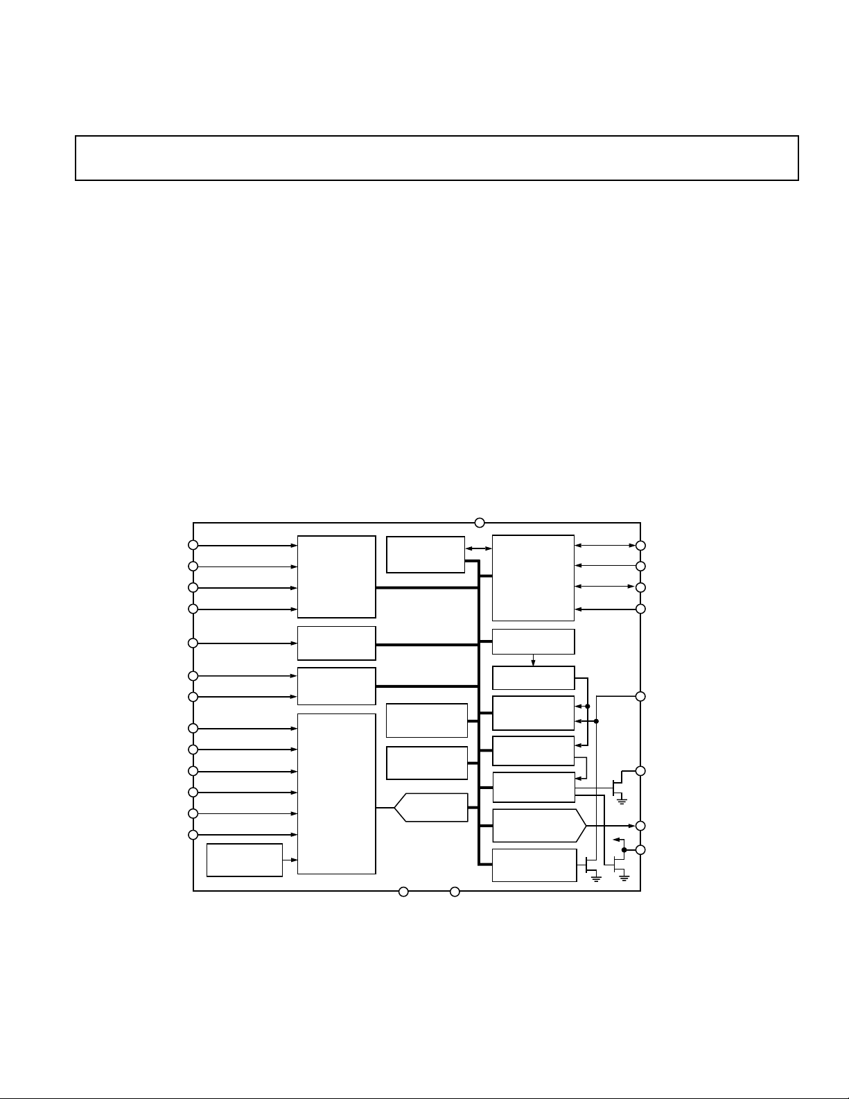
FUNCTIONAL BLOCK DIAGRAM
System Hardware Monitor
ADM9240
PRODUCT DESCRIPTION
The ADM9240 is a complete system hardware monitor for
microprocessor-based systems, providing measurement and
limit comparison of up to four power supplies and two processor core voltages, plus temperature, two fan speeds and chassis
intrusion. Measured values can be read out via an I
ible serial System Management Bus, and values for limit comparisons can be programmed in over the same serial bus. The
high speed successive approximation ADC allows frequent
sampling of all analog channels to ensure a fast interrupt
response to any out-of-limit measurement.
The ADM9240’s 2.85 V to 5.75 V supply voltage range, low
supply current and I
2
C compatible interface, make it ideal for a
wide range of applications. These include hardware monitoring
and protection applications in personal computers, electronic
test equipment and office electronics.
V
CC
2
C-compat-
VID0
VID1
VID2
VID3
VID4
FAN1
FAN2 CI
+V
CCP1
+2.5V
IN
+3.3V
IN
+5V
IN
+12V
IN
+V
CCP2
BANDGAP
TEMPERATURE
SENSOR
VID0 - 3 AND
FAN DIVISOR
REGISTERS
VID4 AND
DEVICE ID
REGISTER
FAN SPEED
COUNTER
INPUT
ATTENUATORS
AND
ANALOG
MULTIPLEXER
SERIAL BUS
ADDRESS
REGISTER
ADDRESS
POINTER
REGISTER
TEMPERATURE
CONFIGURATION
REGISTER
9-BIT ADC
ADM9240
GNDA GNDD
SERIAL BUS
INTERFACE
VALUE AND LIMIT
REGISTERS
LIMIT
COMPARATORS
INTERRUPT
STATUS
REGISTERS
INT MASK
REGISTERS
CONFIGURATION
REGISTER
ANALOG
OUTPUT REGISTER
AND 8-BIT DAC
CHASSIS
INTRUSION
CLEAR REGISTER
NTEST_OUT/A0
A1
SDA
SCL
INT
NTEST_IN/AOUT
RESET
I2C is a registered trademark of Philips Corporation.
REV. 0
Information furnished by Analog Devices is believed to be accurate and
reliable. However, no responsibility is assumed by Analog Devices for its
use, nor for any infringements of patents or other rights of third parties
which may result from its use. No license is granted by implication or
otherwise under any patent or patent rights of Analog Devices.
One Technology Way, P.O. Box 9106, Norwood, MA 02062-9106, U.S.A.
Tel: 781/329-4700 World Wide Web Site: http://www.analog.com
Fax: 781/326-8703 © Analog Devices, Inc., 1998
Page 2

1, 2
ADM9240–SPECIFICA TIONS
(TA = T
Parameter Min Typ Max Units Test Conditions/Comments
POWER SUPPLY
Supply Voltage, V
Supply Current, I
CC
CC
2.85 5 5.75 V
TEMPERATURE-TO-DIGITAL CONVERTER
Accuracy ± 3 °C –40°C ≤ T
Resolution ±0.5 °C
ANALOG-TO-DIGITAL CONVERTER
(INCLUDING MUX AND ATTENUATORS)
Total Unadjusted Error, TUE ±2 % Note 3
Differential Nonlinearity, DNL ±1 LSB
Power Supply Sensitivity ±1 %/V
Total Monitoring Cycle Time 311 331 µs +25°C ≤ T
Input Resistance 100 140 200 kΩ
ANALOG OUTPUT
Output Voltage Range 0 1.25 V
Total Unadjusted Error, TUE ±3% I
Full-Scale Error ±1 ±3%
Zero Error 2 LSB No Load
Differential Nonlinearity, DNL ±1 LSB
Integral Nonlinearity ±1 LSB Monotonic by Design
Output Source Current 2 mA
Output Sink Current 1 mA
FAN RPM-TO-DIGITAL CONVERTER
Accuracy ±6 % +25°C ≤ T
Full-Scale Count 255
FAN1 and FAN2 Nominal Input RPM 8800 rpm Divisor = 1, Fan Count = 153
Internal Clock Frequency 21.1 22.5 23.9 kHz +25°C ≤ T
19.8 22.5 25.2 kHz –40oC ≤ TA ≤ +125°C
DIGITAL OUTPUT NTEST_OUT
Output High Voltage, V
OH
2.4 V I
2.4 V I
Output Low Voltage, V
OL
OPEN-DRAIN DIGITAL OUTPUTS
(INT, RESET, CI)
Output Low Voltage, V
High Level Output Current, I
OL
OH
RESET and CI Pulsewidth 20 45 ms
to T
MIN
, VCC = V
MAX
MIN
to V
, unless otherwise noted)
MAX
1.4 2.0 mA Interface Inactive, ADC Active
1.0 mA ADC Inactive, DAC Active
25 100 µA Shutdown Mode
≤ +125°C
A
±2 °C T
311 353 µs –40°C ≤ T
±12 % –40
= +25°C
A
≤ +125°C (Note 4)
A
≤ +125°C (Note 4)
A
= 2 mA
L
≤ +125°C
A
o
C ≤ TA ≤ +125°C
(Note 5)
4400 rpm Divisor = 2, Fan Count = 153
(Note 5)
2200 rpm Divisor = 3, Fan Count = 153
(Note 5)
1100 rpm Divisor = 4, Fan Count = 153
(Note 5)
≤ +125°C
A
= 5.0 mA,
OUT
= 4.25 V–5.75 V
V
CC
= 3.0 mA,
OUT
= 2.85 V–3.45 V
V
0.4 V I
0.4 V I
CC
= –5.0 mA,
OUT
= 4.25 V–5.75 V
V
CC
= –3.0 mA,
OUT
VCC = 2.85 V–3.45 V
0.4 V I
0.4 V I
0.1 100 µAV
= –5.0 mA, VCC = 5.75 V
OUT
= –3.0 mA, VCC = 3.45 V
OUT
= V
OUT
CC
–2– REV. 0
Page 3

ADM9240
Parameter Min Typ Max Units Test Conditions/Comments
OPEN-DRAIN SERIAL DATA BUS
OUTPUT (SDA)
Output Low Voltage, V
OL
0.4 V I
0.4 V I
High Level Output Current, I
OH
0.1 100 µAV
SERIAL BUS DIGITAL INPUTS
(SCL, SDA)
Input High Voltage, V
Input Low Voltage, V
IL
IH
0.7 × V
CC
0.3 × V
CC
V
V
Hysteresis 500 mV
DIGITAL INPUT LOGIC LEVELS
(A0, A1, CI, RESET, VID0 – VID4,
FAN1, FAN2)
Input High Voltage, V
Input Low Voltage, V
IL
Input High Voltage, V
Input Low Voltage, V
IL
IH
IH
2.4 V VCC = 4.25 V–5.75 V
0.8 V VCC = 4.25 V–5.75 V
2.0 V VCC = 2.85 V–3.45 V
0.4 V VCC = 2.85 V–3.45 V
NTEST_IN
Input High Voltage, V
Input High Voltage, V
IH
IH
2.4 V VCC = 4.25 V–5.75 V
2.0 V VCC = 2.85 V–3.45 V
DIGITAL INPUT CURRENT
Input High Current, I
Input High Current, A0, A1, I
Input Low Current, I
Input Capacitance, C
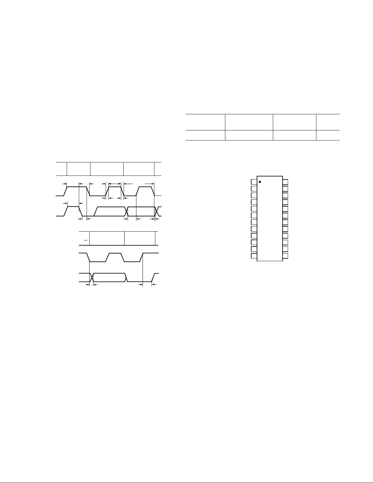
SERIAL BUS TIMING
Clock Frequency, f
Glitch Immunity, t
Bus Free Time, t
Start Setup Time, t
Start Hold Time, t
SCL Low Time, t
SCL High Time, t
SCL, SDA Rise Time, t
SCL, SDA Fall Time, t
Data Setup Time, t
Data Hold Time, t
NOTES
1
All voltages are measured with respect to GND, unless otherwise noted.
2
Typicals are at TA = +25°C and represent most likely parametric norm. Shutdown current typ is measured with VCC = 3.3 V.
3
TUE (Total Unadjusted Error) includes Offset, Gain and Linearity errors of the ADC, multiplexer and on-chip input attenuators, including an external series input
protection resistor value between zero and 1 k Ω.
4
Total monitoring cycle time is the time taken to measure all six analog inputs plus the temperature sensor.
5
The total fan count is based on 2 pulses per revolution of the fan tachometer output.
6
A0 and A1 have internal 75 kΩ pull-down.
7
Timing specifications are tested at logic levels of V
Specifications subject to change without notice.
SCLK
SW
BUF
SU;STA
HD;STA
LOW
HIGH
SU;DAT
HD;DAT
IH
IH
IL
IN
7
R
F
= 0.3 × VCC for a falling edge and V
IL
–1 µAV
–200 75 µAV
1 µAV
20 pF
400 kHz See Figure 1
50 ns See Figure 1
1.3 µs See Figure 1
600 ns See Figure 1
600 ns See Figure 1
1.3 µs See Figure 1
0.6 µs See Figure 1
300 ns See Figure 1
300 µs See Figure 1
100 ns See Figure 1
900 ns See Figure 1
= 0.7 × VCC for a rising edge.
IH
= –3.0 mA,
OUT
= 4.25 V–5.75 V
V
CC
= –3.0 mA
OUT
= 2.85 V–3.45 V
V
CC
= V
OUT
IN
IN
IN
= V
= V
= 0
CC
CC
(Note 6)
CC
–3–REV. 0
Page 4
ADM9240
TOP VIEW
(Not to Scale)
24
23
22
21
20
19
18
17
16
15
14
13
1
2
3
4
5
6
7
8
9
10
11
12
ADM9240
RESET
NTEST_IN/AOUT
INT
V
CC
GNDD
NTEST_OUT/A0
A1
SDA
SCL
CI
FAN2
FAN1
GNDA
+V
CCP2
+12V
IN
+5V
IN
+3.3V
IN
VID0
VID1
VID2
VID3
+2.5V
IN
+V
CCP1
VID4
ABSOLUTE MAXIMUM RATINGS*
Positive Supply Voltage (VCC) . . . . . . . . . . . . . . . . . . . . . 6.5 V
Voltage on Any Input or Output Pin . . –0.3 V to (V
+ 0.3 V)
CC
(Except Analog Inputs)
16 V V
. . . . . . . . . . . . . . . . . . . . . . . . . . . . . . . . . . . . +16 V
IN
All Other Analog Inputs . . . . . . . . . . . . . . . . . . . . . . . . . +7.5 V
Ground Difference (GNDD–GNDA) . . . . . . . . . . . . ±300 mV
Input Current At Any Pin . . . . . . . . . . . . . . . . . . . . . . . ±5 mA
Package Input Current . . . . . . . . . . . . . . . . . . . . . . . . ±20 mA
Maximum Junction Temperature (T
max) . . . . . . . . . . 150°C
J
Storage Temperature Range . . . . . . . . . . . . .–65°C to +150°C
Lead Temperature, Soldering
Vapor Phase 60 (sec) . . . . . . . . . . . . . . . . . . . . . . . . +215°C
Infrared 15 (sec) . . . . . . . . . . . . . . . . . . . . . . . . . . . +200°C
ESD Rating All Pins Except Pin 15 . . . . . . . . . . . . . . . .2000 V
ESD Rating Pin 15 . . . . . . . . . . . . . . . . . . . . . . . . . . . . . 500 V
PROTOCOL
SCL
SDA
PROTOCOL
Condition
t
SU;STA
t
BUF
Start
(S)
t
HD;STA
Bit 0
LSB
(R/W)
Bit 7
MSB
(A7)
t
t
LOW
t
r
Acknowledge
(A)
HIGH
t
f
1/f
t
SU;DAT
Stop
Condition
Bit 6
(A6)
(P)
SCL
t
HD;DAT
*Stresses above those listed under Absolute Maximum Ratings may cause perma-
nent damage to the device. This is a stress rating only; functional operation of the
device at these or any other conditions above those indicated in the operational
section of this specification is not implied. Exposure to absolute maximum rating
conditions for extended periods may affect device reliability.
THERMAL CHARACTERISTICS
24-Lead Small Outline Package:
= 50°C/Watt, θ
θ
JA
= 10°C/Watt
JC
ORDERING GUIDE
Temperature Package Package
Model Range Description Option
ADM9240ARU –40°C to +125°C 24-Lead TSSOP RU-24
PIN CONFIGURATION
SCL
SDA
t
VD;DAT
Figure 1. Diagram for Serial Bus Timing
t
SU;STO
–4– REV. 0
Page 5

ADM9240
PIN FUNCTION DESCRIPTIONS
Pin Number Mnemonic Description
1 NTEST_OUT/A0 Digital I/O. Dual Function Pin. The lowest order programmable bit of the Serial Bus Address.
This pin functions as an output when doing a NAND Tree test.
2 A1 Digital Input. The highest order programmable bit of the Serial Bus Address.
3 SDA Digital I/O. Serial Bus Bidirectional Data. Open-drain output.
4 SCL Digital Input. Serial Bus Clock.
5 FAN1 Digital Input. 0 to V
6 FAN2 Digital Input. 0 to V
7 CI Digital I/O. An active high input from an external circuit that latches a Chassis Intrusion
event. This line can go high without any clamping action regardless of the powered state of
the ADM9240. The ADM9240 provides an internal open drain on this line, controlled by
Bit 6 of Register 40h or Bit 7 of Register 46h, to provide a minimum 20 ms pulse on this line,
to reset the external Chassis Intrusion Latch.
8 GNDD Digital Ground. Internally connected to all of the digital circuitry.
9V
CC
Power (+2.85 V to +5.75 V). Typically powered from +3.3 V or +5 V power rail. Bypass with
the parallel combination of 10 µF (electrolytic or tantalum) and 0.1 µF (ceramic) bypass
capacitors.
10 INT Digital Output. Interrupt Request (open drain). The output is enabled when Bit 1 of the
Configuration Register is set to 1. The default state is disabled.
11 NTEST_IN/AOUT Digital Input/Analog Output. An active-high input that enables NAND Tree mode board-
level connectivity testing. Refer to section on NAND Tree testing. Also functions as a pro-
grammable analog output when NAND Tree is not selected
12 RESET Digital I/O. Master Reset, 5 mA driver (open drain), active low output with a 20 ms minimum
pulsewidth. Available when enabled via Bit 7 in Register 44h, and set using Bit 4 in Register
40h. Also acts as reset input when pulled low (e.g., power-on reset).
13 GNDA Analog Ground. Internally connected to all analog circuitry. The ground reference for all
analog inputs.
14 +V
CCP2
Analog Input. Monitors processor core voltage +V
monitor the –12 V supply by adding two external resistors.
15 +12 V
16 +5 V
IN
17 +3.3 V
18 +2.5 V
19 +V
CCP1
IN
IN
IN
Analog Input. Monitors +12 V supply.
Analog Input. Monitors +5 V supply.
Analog Input. Monitors +3.3 V supply.
Analog Input. Monitors +2.5 V supply.
Analog Input. Monitors processor core voltage +V
20 VID4 Digital Input. Core Voltage ID readouts from the processor. This value is read into the
VID4 Status Register.
21 VID3 Digital Input. Core Voltage ID readouts from the processor. This value is read into the
VID0–VID3 Status Register.
22 VID2 Digital Input. Core Voltage ID readouts from the processor. This value is read into the
VID0–VID3 Status Register.
23 VID1 Digital Input. Core Voltage ID readouts from the processor. This value is read into the
VID0–VID3 Status Register.
24 VID0 Digital Input. Core Voltage ID readouts from the processor. This value is read into the
VID0–VID3 Status Register.
amplitude fan tachometer input.
CC
amplitude fan tachometer input.
CC
CCP2
CCP1
(0 V–3.6 V). Can also be used to
(0 V–3.6 V).
–5–REV. 0
Page 6

ADM9240
GENERAL DESCRIPTION
The ADM9240 is a complete system hardware monitor for
microprocessor-based systems. The device communicates with
the system via a serial System Management Bus. The serial bus
controller has two hardwired address lines for device selection
(Pin 1 and Pin 2), a serial data line for reading and writing
addresses and data (Pin 3), and an input line for the serial clock
(Pin 4). All control and programming functions of the ADM9240
are performed over the serial bus.
An on-chip analog-to-digital converter with six multiplexed
analog inputs measures power supply voltages (+12 V, +5 V,
+3.3 V, +2.5 V—Pins 15 to 18) and processor core voltages
CCP1
and +V
(+V
input from an on-chip bandgap temperature sensor that monitors system ambient temperature.
Two count inputs (Pins 5 and 6) are provided for monitoring
the speed of fans with tachometer outputs. To accommodate
fans with different speeds and different tacho outputs, a divisor
of 1, 2, 4 or 8 can be programmed into the counter.
Five digital inputs (VID4 to VID0—Pins 20 to 24) read the
processor Voltage ID code, while a chassis intrusion input
(Pin 7) is provided to detect unauthorized tampering with the
equipment.
When the ADM9240 monitoring sequence is started, it cycles
sequentially through the measurement of analog inputs and the
temperature sensor, while at the same time the fan speed inputs
are independently monitored. Measured values from these inputs are stored in value registers. These can be read out over the
serial bus, or can be compared with programmed limits stored
in the limit registers. The results of out-of-limit comparisons are
stored in the interrupt status registers and will generate an interrupt on the INT line (Pin 10).
Any or all of the Interrupt Status Bits can be masked by appropriate programming of the Interrupt Mask Register.
A RESET input/output (Pin 12) is provided. Pulling this pin
low will reset all ADM9240 internal registers to default values.
The ADM9240 can also be programmed to give a low-going
20 ms reset pulse at this pin.
The ADM9240 contains an on-chip, 8-bit digital-to-analog
converter with an output range of zero to 1.25 V (Pin 11). This
is typically used to implement a temperature-controlled fan by
controlling the speed of a fan dependent upon the temperature
measured by the on-chip temperature sensor.
Testing of board level connectivity is simplified by providing a
NAND tree test function. The AOUT (Pin 11) also doubles as
a NAND test input, while Pin 1 doubles as a NAND tree output.
—Pins 19 and 14). The ADC also accepts
CCP2
INTERNAL REGISTERS OF THE ADM9240
A brief description of the ADM9240’s principal internal registers is given below. More detailed information on the function
of each register is given in Tables V to XVII.
Configuration Register: Provides control and configuration.
Serial Address Register: Stores the serial bus address of the
ADM9240.
Address Pointer Register: Contains the address that selects
one of the other internal registers. When writing to the ADM9240,
the first byte of data is always a register address, which is written
to the Address Pointer Register.
Interrupt (INT) Status Registers: Two registers to provide
status of each Interrupt event.
Interrupt (INT) Mask Registers: Allow masking of individual Interrupt sources.
Temperature Configuration Register: The configuration of
the temperature interrupt is controlled by the lower three bits of
this register.
VID/Fan Divisor Registers: The status of the VID0 to VID4
pins of the processor can be written to and read from these
registers. Divisor values for fan-speed measurement are also
stored in one of these registers.
Value and Limit Registers: The results of analog voltage
inputs, temperature and fan speed measurements are stored in
these registers, along with their limit values.
Analog Output Register: The code controlling the analog
output DAC is stored in this register.
Chassis Intrusion Clear Register: A signal latched on the
chassis intrusion pin can be cleared by writing to this register.
–6– REV. 0
Page 7
ADM9240
SERIAL BUS INTERFACE
Control of the ADM9240 is carried out via the serial bus. The
ADM9240 is connected to this bus as a slave device, under the
control of a master device, e.g., the PIIX4.
The ADM9240 has a 7-bit serial bus address. When the device
is powered up, it will do so with a default serial bus address.
The five MSBs of the address are set to 01011, the two LSBs
are determined by the logical states of Pin 1(NTEST_OUT/A0)
and Pin 2 (A1) at power-up. These pins have internal 75 kΩ
pull-down resistors, so if they are left open-circuit the default
address will be 0101100.
The facility to make hardwired changes to A1 and A0 allows the
user to avoid conflicts with other devices sharing the same serial
bus, for example if more than one ADM9240 is used in a system. Once the ADM9240 has been powered up, the five MSBs
of the serial bus address may be changed by writing a 7-bit word
to the serial Address Pointer Register (the hardwired values of
A0 and A1 cannot be overwritten). Thereafter, the new serial
bus address must be used to select the ADM9240, until it is
changed again, or the device is powered off.
The serial bus protocol operates as follows:
1. The master initiates data transfer by establishing a START
condition, defined as a high-to-low transition on the serial
data line SDA while the serial clock line SCL remains high.
This indicates that an address/data stream will follow. All
slave peripherals connected to the serial bus respond to the
START condition, and shift in the next eight bits, consisting
of a 7-bit address (MSB first) plus an R/W bit, which determines the direction of the data transfer, i.e., whether data
will be written to or read from the slave device.
The peripheral whose address corresponds to the transmitted
address responds by pulling the data line low during the low
period before the ninth clock pulse, known as the acknowledge bit. All other devices on the bus now remain idle while
the selected device waits for data to be read from or written
to it. If the R/W bit is a 0, the master will write to the slave
device. If the R/W bit is a 1, the master will read from the
slave device.
2. Data is sent over the serial bus in sequences of nine clock
pulses, eight bits of data followed by an acknowledge bit
from the slave device. Transitions on the data line must
occur during the low period of the clock signal and remain
stable during the high period, as a low-to-high transition
when the clock is high may be interpreted as a STOP signal.
The number of data bytes that can be transmitted over the
serial bus in a single READ or WRITE operation is limited
only by what the master and slave devices can handle.
3. When all data bytes have been read or written, stop conditions are established. In WRITE mode, the master will pull
the data line high during the tenth clock pulse to assert a
STOP condition. In READ mode, the master device will
override the acknowledge bit by pulling the data line high
during the low period before the ninth clock pulse. This is
known as No Acknowledge. The master will then take the
data line low during the low period before the tenth clock
pulse, then high during the tenth clock pulse to assert a
STOP condition.
Any number of bytes of data may be transferred over the serial
bus in one operation, but it is not possible to mix read and write
in one operation, because the type of operation is determined at
the beginning and cannot subsequently be changed without
starting a new operation.
In the case of the ADM9240, write operations contain either
one or two bytes, and read operations contain one byte and
perform the following functions:
To write data to one of the device data registers or read data
from it, the Address Pointer Register must be set so that the
correct data register is addressed, then data can be written into
that register or read from it. The first byte of a write operation
always contains an address that is stored in the Address Pointer
Register. If data is to be written to the device, then the write
operation contains a second data byte that is written to the
register selected by the Address Pointer Register.
This is illustrated in Figure 2a. The device address is sent over
the bus followed by R/W set to 0. This is followed by two data
bytes. The first data byte is the address of the internal data
register to be written to, which is stored in the Address Pointer
Register. The second data byte is the data to be written to the
internal data register.
SCL
SDA
START BY
MASTER
19
0
1 0 1 1 A1 A0 D7
FRAME 1
SERIAL BUS ADDRESS BYTE
SCL (CONTINUED)
SDA (CONTINUED)
R/W
ACK. BY
ADM9240
1
1
D7 D6
D6
D5 D4 D3
ADDRESS POINTER REGISTER BYTE
D5 D4 D3
FRAME 2
FRAME 3
DATA BYTE
D2
D2
D1 D0
D1
ACK. BY
ADM9240
D0
9
9
ACK. BY
ADM9240
STOP BY
MASTER
Figure 2a. Writing a Register Address to the Address Pointer Register, then Writing Data to the Selected Register
–7–REV. 0
Page 8

ADM9240
When reading data from a register there are two possibilities:
1. If the ADM9240’s Address Pointer Register value is unknown or not the desired value, it is first necessary to set it to
the correct value before data can be read from the desired
data register. This is done by performing a write to the
ADM9240 as before, but only the data byte containing the
register address is sent, as data is not to be written to the
register. This is shown in Figure 2b.
A read operation is then performed consisting of the serial
bus address, R/W bit set to 1, followed by the data byte read
from the data register. This is shown in Figure 2c.
2. If the Address Pointer Register is known to be already at the
desired address, data can be read from the corresponding
data register without first writing to the Address Pointer
Register, so Figure 2b can be omitted.
Notes:
1. Although it is possible to read a data byte from a data register
without first writing to the Address Pointer Register, if the
Address Pointer Register is already at the correct value, it is
not possible to write data to a register without writing to the
Address Pointer Register, because the first data byte of a
write is always written to the Address Pointer Register.
191
SCL
2. In Figures 2a to 2c, the serial bus address is shown as the
default value 01011(A1)(A0), where A1 and A0 are
hardwired to either Logic 0 or Logic 1.
ANALOG INPUTS
The ADM9240 has six analog inputs. Four of these are dedicated to monitoring the following power supply voltages: +12 V,
+5 V, +3.3 V, +2.5 V.
These inputs are multiplexed into the on-chip, successive approximation, analog-to-digital converter. This has a resolution
of ten bits, but only eight bits are used for the voltage measurement and limit comparison. The basic input range of the ADC
is 0 V to 2.5 V, and the power supply inputs are scaled by onchip attenuators such that the ADC produces an output of 3/4 ×
full scale or 192 decimal, when the input voltage is at its nominal value. The use of on-chip scaling guarantees accuracy and
removes the need for precision external resistors.
9
SDA
START BY
MASTER
SCL
SDA
START BY
MASTER
0
10
SERIAL BUS ADDRESS BYTE
1A1A0 D7
1
FRAME 1
R/W
ACK. BY
ADM9240
D6
D4 D3 D2 D1
D5
ADDRESS POINTER REGISTER BYTE
FRAME 2
D0
ACK. BY
ADM9240
Figure 2b. Writing to the Address Pointer Register only
191
0
10
SERIAL BUS ADDRESS BYTE
1A1A0 D7
1
FRAME 1
R/W
ACK. BY
ADM9240
D6 D5
D4 D3 D2 D1
DATA BYTE FROM ADM9240
FRAME 2
D0
BY MASTER
Figure 2c. Reading Data from a Previously Selected Register
9
NO ACK.
STOP BY
MASTER
STOP BY
MASTER
–8– REV. 0
Page 9

The input ranges of the analog inputs are shown in more detail
MUX
+V
CCP2
97.3kV
50pF
42.7kV
+5V
22.7kV
35pF
122.2kV
55.2kV
25pF
91.6kV
80.9kV
25pF
61.1kV
111.2kV
25pF
36.7kV
97.3kV
50pF
42.7kV
+12V
+3.3V
+2.5V
+V
CCP1
in Table I.
The +V
CCP1
and +V
inputs are used to measure processor
CCP2
core voltages, and have an input range from 0 V to 3.6 V. If
only a single processor core voltage is being monitored, the
input may be used to monitor the –12V supply. This is
V
CCP2
achieved by using a resistive divider network referenced to a
known positive dc voltage. This is illustrated in Figure 4.
INPUT CIRCUITS
The internal structure for the analog inputs is shown in Figure
3. Each input circuit consists of an input protection diode, an
attenuator, plus a capacitor to form a first order low-pass filter
which gives the input immunity to high frequency noise.
ADM9240
Figure 3. Internal Structure of Analog Inputs
Table I. A/D Output Code vs. V
IN
Input Voltage A/D Output
+12 V
IN
+5 V
IN
+3.3 V
IN
+2.5 V
IN
+V
CCP1
+V
CCP2
Decimal Binary
<0.062 <0.026 <0.0172 <0.013 <0.014 <0.014 0 00000000
0.062–0.125 0.026–0.052 0.017–0.034 0.013–0.026 0.014–0.028 0.014–0.028 1 00000001
0.125–0.187 0.052–0.078 0.034–0.052 0.026–0.039 0.028–0.042 0.028–0.042 2 00000010
0.188–0.250 0.078–0.104 0.052–0.069 0.039–0.052 0.042–0.056 0.042–0.056 3 00000011
0.250–0.313 0.104–0.130 0.069–0.086 0.052–0.065 0.056–0.070 0.056–0.070 4 00000100
0.313–0.375 0.130–0.156 0.086–0.103 0.065–0.078 0.070–0.084 0.070–0.084 5 00000101
0.375–0.438 0.156–0.182 0.103–0.120 0.078–0.091 0.084–0.098 0.084–0.098 6 00000110
0.438–0.500 0.182–0.208 0.120–0.138 0.091–0.104 0.098–0.112 0.098–0.112 7 00000111
0.500–0.563 0.208–0.234 0.138–0.155 0.104–0.117 0.112–0.126 0.112–0.126 8 00001000
l
l
l
4.000–4.063 1.666–1.692 1.100–1.117 0.833–0.846 0.900–0.914 0.900–0.914 64 (1/4 Scale) 01000000
l
l
l
8.000–8.063 3.330–3.560 2.200–2.217 1.667–1.680 1.800–1.814 1.800–1.814 128 (1/2 Scale) 10000000
l
l
12.000–12.063 5.000–5.026 3.300–3.317 2.500–2.513 2.700–2.714 2.700–2.714 192 (3/4 Scale) 11000000
15.313–15.375 6.380–6.406 4.210–4.230 3.190–3.203 3.445–3.459 3.445–3.459 245 11110101
15.375–15.438 6.406–6.432 4.230–4.245 3.203–3.216 3.459–3.473 3.459–3.473 246 11110110
15.438–15.500 6.432–6.458 4.245–4.263 3.216–3.229 3.473–3.487 3.473–3.487 247 11110111
15.500–15.563 6.458–6.484 4.263–4.280 3.229–3.242 3.487–3.501 3.487–3.501 248 11111000
15.563–15.625 6.484–6.510 4.280–4.300 3.242–3.255 3.501–3.515 3.501–3.515 249 11111001
15.625–15.688 6.510–6.536 4.300–4.314 3.255–3.268 3.515–3.529 3.515–3.529 250 11111010
15.688–15.750 6.536–6.562 4.314–4.331 3.268–3.281 3.529–3.543 3.529–3.543 251 11111011
15.750–15.813 6.562–6.588 4.331–4.348 3.281–3.294 3.543–3.558 3.543–3.558 252 11111100
15.813–15.875 6.588–6.615 4.348–4.366 3.294–3.307 3.558–3.572 3.558–3.572 253 11111101
15.875–15.938 6.615–6.640 4.366–4.383 3.307–3.320 3.572–3.586 3.572–3.586 254 11111110
>15.938 >6.640 >4.383 >3.320 >3.586 >3.586 2 55 11111111
l
l
l
l
–9–REV. 0
Page 10

ADM9240
SETTING OTHER INPUT RANGES
If any of the inputs is unused, and there is a requirement for
monitoring another power supply such as –12 V, the input range
of the unused input can easily be scaled and offset to accommodate this. For example, if only one processor core voltage is to
be monitored, the unused V
input can be used to monitor
CCP
another supply voltage.
If the voltage to be monitored is positive, it is simply a matter of
using an input with a lower full scale than the voltage to be
measured and adding an external input attenuator, but bear in
mind that the input resistance (≈140 kΩ) of the on-chip attenuator will load the external attenuator. This can be accounted for
in the calculation, but the values of the on-chip attenuator resistors are not precise and vary with temperature. Therefore, the
external attenuator should have a much lower output resistance
to minimize the loading. If this is not acceptable, a buffer amplifier can be used.
If the input voltage range is negative, it must first be converted
to a positive voltage. The simplest way to do this is simply to
attenuate and offset the voltage, as shown in Figure 4, which
shows the +V
input scaled to measure a –12 V input. Using
CCP2
the values shown, the input range is zero to –13.5 V, which will
accommodate a +12.5% tolerance on the nominal value.
+5V
R2
R1
–13.2V TO 0V IN
2.7kV
0V TO 3.6V
Figure 4. Scaling V
1kV
+V
CCP2
R3
39kV
to –12 V (+10%)
CCP2
<140kV
The resistor ratios are calculated as follows:
R1/R2 = |V–|(max)/V+
(to give zero volts at the input for the most negative value of V–.
R2 has no effect under this condition as the voltage across it is
zero)
and:
(V+ – V
(to give a voltage V
)/VFS = R2/RP = (R1 and R2 in Parallel)
FS
at the input when V– is zero, where VFS is
FS
the normal full-scale voltage of the input used).
This is a simple and cheap solution, but the following points
should be noted.
1. Since the input signal is not inverted, an increase in the magnitude of the –12V supply (going more negative), will cause
the input voltage to fall and give a lower output code from
the ADC. Conversely, a decrease in the magnitude of the
–12 V supply will cause the ADC code to increase. This
means that the upper and lower limits will be transposed.
2. Since the offset voltage is derived from the +5 V supply,
variations in this supply will affect the ADC code.
It is therefore a good idea to read the value of the +5 V supply and adjust the limits for the –12V supply accordingly.
The 5 V supply is attenuated by a factor R
is the parallel combination of R1 and R3. An increase in
R
P
/(R2+RP), where
P
the 5 V supply increases the ADC input by the DV × RP/
(R2+R
), while a decrease in the 5 V supply correspondingly
P
decreases the input to the ADC.
3. The on-chip input attenuators will load the external attenuator, as mentioned earlier.
This technique can be applied to any other unused input. By
suitable choice of V+ and the input resistors, a variety of negative and/or bipolar input ranges can be obtained.
TEMPERATURE MEASUREMENT SYSTEM
The ADM9240 contains an on-chip bandgap temperature sensor. The on-chip ADC performs 9-bit conversions on the output
of this sensor and outputs the temperature data in 9-bit twos
complement format, but only the eight most significant bits are
used for temperature limit comparison. The full 9-bit temperature data can be obtained by reading the 8 MSBs from the Temperature Value Register (Address 27h) and the LSB from Bit 7
of the Temperature Configuration Register (Address 4Bh).
The format of the temperature data is shown in Table II. Theoretically, the temperature sensor and ADC can measure temperatures from –128°C to +127°C with a resolution of 0.5°C,
although temperatures below –40°C and above +125°C are
outside the operating temperature range of the device.
Table II. Temperature Data Format
Temperature Digital Output
–128°C 1 0000 0000
–125°C 1 0000 0110
–100°C 1 0011 1000
–75°C 1 0110 1010
–50°C 1 1001 1100
–25°C 1 1100 1110
–0.5°C 1 1111 1111
0°C 0 0000 0000
+0.5°C 0 0000 0001
+10°C 0 0001 0100
+25°C 0 0011 0010
+50°C 0 0110 0100
+75°C 0 1001 0110
+100°C 0 1100 1000
+125°C 0 1111 1010
+127°C 0 1111 1111
LIMIT VALUES
Limit values for analog measurements are stored in the appropriate limit registers. In the case of voltage measurements, high
and low limits can be stored so that an interrupt request will be
generated if the measured value goes above or below acceptable
values. In the case of temperature, a Hot Temperature Limit
can be programmed, and a Hot Temperature Hysteresis Limit,
which will usually be some degrees lower. This can be useful as
it allows the system to be shut down when the hot limit is exceeded, and automatically restarted when it has cooled down to
a safe temperature.
–10– REV. 0
Page 11

ADM9240
MONITORING CYCLE TIME
The monitoring cycle begins when a one is written to the Start
Bit (Bit 0), and a zero to the INT_Clear Bit (Bit 3) of the Configuration Register. INT_Enable (Bit 1) should be set to one to
enable the INT output. The ADC measures each analog input
in turn, starting with V
and finishing with the on-chip tem-
CCP2
perature sensor. As each measurement is completed the result
is automatically stored in the appropriate value register. This
“round-robin” monitoring cycle continues until it is disabled by
writing a 0 to Bit 0 of the Configuration Register.
The counter controlling the multiplexer is driven by an on-chip
clock of nominally 22.5 kHz, so the entire measurement sequence
takes (nominally):
µ
s × 7 = 310.8 µs
44.4
This rapid sampling of the analog inputs ensures a quick response in the event of any input going out of limits, unlike other
monitoring chips that employ slower ADCs.
When a monitoring cycle is started, monitoring of the fan speed
inputs begins at the same time as monitoring of the analog inputs. However, the two monitoring cycles are not synchronized
in any way, and the monitoring cycle time for the fan inputs is
dependent on fan speed and much slower than for the analog
inputs. For more details see the Fan Speed Measurement section.
INPUT SAFETY
Scaling of the analog inputs is performed on-chip, so external
attenuators are normally not required. However, since the
power supply voltages will appear directly at the pins, it is advisable to add small external resistors in series with the supply
traces to the chip to prevent damaging the traces or power supplies should an accidental short such as a probe connect two
power supplies together.
As the resistors will form part of the input attenuators, they will
affect the accuracy of the analog measurement if their value is
too high. The analog input channels are calibrated assuming an
external series resistor of 500 Ω, and the accuracy will remain
within specification for any value from zero to 1 kΩ, so a standard 510 Ω resistor is suitable.
The worst such accident would be connecting –12 V to +12 V—
a total of 24 V difference, with the series resistors this would
draw a maximum current of approximately 24 mA.
ANALOG OUTPUT
The ADM9240 has a single analog output from an unsigned
8-bit DAC which produces 0 V–1.25 V. The analog output
register defaults to FF during power-on reset, which produces
maximum fan speed. The analog output may be amplified and
buffered with external circuitry such as an op amp and transistor
to provide fan speed control.
A suitable drive circuit is given in Figure 5.
Care must be taken when choosing the op amp to ensure that its
input common-mode range and output voltage swing are suitable.
The op amp may be powered from the +12 V rail alone or from
±12 V. If it is powered from +12 V then the input commonmode range should include ground to accommodate the minimum output voltage of the DAC, and the output voltage should
swing below 0.6 V to ensure that the transistor can be turned
fully off.
If the op amp is powered from –12 V, precautions such as a
clamp diode to ground may be needed to prevent the baseemitter junction of the transistor being reverse-biased in the
unlikely event that the output of the op amp should swing negative for any reason.
The positive output swing of the op amp should be as close to
+12 V as possible so that the maximum voltage can be obtained
from the transistor. Even if the op amp swings to the rail, the
maximum voltage from the emitter of the transistor will be
about 11.4 V. typical values for this condition would be:
Gain = 11.4/1.25 = 9.12 = 1 + R1/R2
R1 = 82 kΩ, R2 = 10 kΩ (nearest preferred value)
giving an actual gain of 9.2.
The transistor should have a reasonably high h
to avoid its
FE
base current pulling down the output of the op amp, it must
have an I
greater than the maximum fan current and be
CMAX
capable of dissipating power due to the voltage dropped across it
when the fan is not operating at full speed. Depending on the
fan parameters, some suitable devices would be 2N2219A,
2N3019 or ZTX450.
+12V
NTEST_IN/AOUT
R1
R2
Figure 5. Analog Output Driving Fan
LAYOUT AND GROUNDING
Analog inputs will provide best accuracy when referred to the
GNDA pin. A separate, low impedance ground plane for analog
ground, which provides a ground point for the voltage dividers
and analog components, will provide best performance but is
not mandatory.
The power supply bypass, the parallel combination of 10 µF
(electrolytic or tantalum) and 0.1 µF (ceramic) bypass capaci-
tors connected between Pin 9 and ground, should also be located as close as possible to the ADM9240.
–11–REV. 0
Page 12

ADM9240
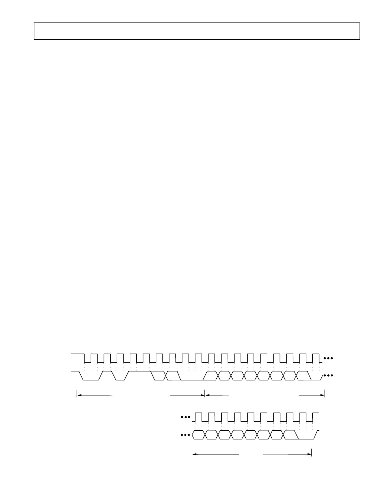
22.5kHz
CLOCK
CONFIG
REG. BIT 0
FAN1
INPUT
FAN1
MEASUREMENT
PERIOD
FAN2
MEASUREMENT
PERIOD
START OF
MONITORING
CYCLE
FAN2
INPUT
FAN INPUTS
Two inputs are provide for monitoring the condition of cooling
fans. Signal conditioning in the ADM9240 accommodates the
slow rise and fall times typical of fan tachometer outputs. The
maximum input signal range is 0 to V
inputs are supplied from fan outputs that exceed 0 to V
. In the event that these
CC
CC
,
either resistive attenuation of the fan signal or diode clamping
must be included to keep inputs within an acceptable range.
Figures 6a to 6c show circuits for most common fan tacho
outputs.
If the fan tacho output has a resistive pull-up to V
it can be
CC
connected directly to the fan input, as shown in Figure 6a.
+12V
PULL-UP
4.7kV
TYP.
TACHO
OUTPUT
FAN1
OR FAN2
Figure 6a. Fan with Tachometer Pull-Up to +V
V
CC
FAN SPEED
COUNTER
CC
If the fan output has a resistive pull-up to +12 V (or other
voltage greater than V
), the fan output can be clamped with
CC
a Zener diode, as shown in Figure 6b. The Zener voltage
should be chosen so that it is greater than V
, allowing for the voltage tolerance of the Zener. A value of
V
CC
about 0.8 × V
+12V
is suitable.
CC
*CHOOSE ZD1 VOLTAGE APPROX. 0.8 3 V
PULL-UP
4.7kV
TYP.
TACHO
OUTPUT
ZD1*
ZENER
FAN1
OR FAN2
but less than
IH
V
CC
CC
FAN SPEED
COUNTER
Figure 6b. Fan with Tachometer Pull-Up to Voltage >V
(e.g., 12 V) Clamped with Zener Diode
If the fan has a strong pull-up (less than 1 kΩ) to +12 V, or a
totem-pole output, a series resistor can be added to limit the
zener current, as shown in Figure 6c. Alternatively, a resistive
attenuator may be used, as shown in Figure 6d.
R1 and R2 should be chosen such that:
2 V < V
PULL-UP
× R2/(R
+ R1 + R2) < V
PULL-UP
CC
If the value of the pull-up resistor is not known, the value of R1
and R2 should be made fairly large, but not so large that the
input leakage current will cause a large voltage drop across
them.
With a pull-up voltage of 12 V and pull-up resistor less than
1 kΩ, suitable values for R1 and R2 would be 100 kΩ and
47 kΩ. This will give a high input voltage of 3.83 V.
+12V
*CHOOSE ZD1 VOLTAGE APPROX. 0.8 3 V
TACHO
OUTPUT
PULL-UP
TYP. < 1kV
OR TOTEM-POLE
R1
10kV
FAN1
OR FAN2
ZD1*
ZENER
V
CC
CC
FAN SPEED
COUNTER
Figure 6c. Fan with Strong Tachometer Pull-Up to
>V
or Totem-Pole Output, Clamped with Zener and
CC
Resistor
+12V
< 1kV
R1*
TACHO
OUTPUT
*SEE TEXT
FAN1
OR FAN2
R2*
V
CC
FAN SPEED
COUNTER
Figure 6d. Fan with Strong Tachometer Pull-Up to
>V
or Totem-Pole Output, Attenuated with R1/R2
CC
INPUT CURRENT LIMITING
If the fans are powered while the ADM9240 is unpowered, the
inputs of the ADM9240 will try to clamp the fan output voltage. In this case the input current must be limited to less than
the maximum value in the Absolute Maximum Ratings table.
The pull-up resistor of the fan tacho output may provide this
current limiting but, if its value is too low, it may be necessary
to add additional resistance in series with the fan input pins.
FAN SPEED MEASUREMENT
The fan counter does not count the fan tacho output pulses
directly, because the fan speed may be less than 1000 rpm and
it would take several seconds to accumulate a reasonably large
and accurate count. Instead, the period of the fan revolution is
measured by gating an on-chip 22.5 kHz oscillator into the
input of an 8-bit counter for two periods of the fan tacho output, as shown in Figure 7, so the accumulated count is actually
proportional to the fan tacho period and inversely proportional
to the fan speed.
The monitoring cycle begins when a one is written to the start
bit (Bit 0), and a zero to the INT_Clear bit (Bit 3) of the Configuration Register INT_Enable (Bit 1) should be set to one to
enable the INT output. The measurement begins on the rising
CC
edge of a fan tacho pulse, and ends on the next-but-one rising
edge. Once the fan speeds have been measured, they will be
stored in the Fan Speed Value Registers and can be read at any
time. The measurements will be updated as long as the monitoring cycle continues.
Figure 7. Fan Speed Measurement
–12– REV. 0
Page 13

ADM9240
To accommodate fans of different speed and/or different numbers of output pulses per revolution, a prescaler (divisor) of 1, 2,
4 or 8 may be added before the counter. The default value is 2,
which gives a count of 153 for a fan running at 4400 rpm producing two output pulses per revolution.
The count is calculated by the equation:
3
Count = (22.5 × 10
× 60) /(rpm × Divisor)
For constant speed fans, fan failure is normally considered to
have occurred when the speed drops below 70% of nominal,
which would correspond to a count of 219. Full scale (255)
would be reached if the fan speed fell to 60% of its nominal
value. For temperature controlled variable speed fans the situation will be different.
Table III shows the relationship between fan speed and time per
revolution at 60%, 70% and 100% of nominal rpm for fan
speeds of 1100 rpm, 2200 rpm, 4400 rpm and 8800 rpm, and
the divisor that would be used for each of these fans, based on
two tacho pulses per revolution.
Table III. Fan Speeds and Divisors
Time per Time per Time per
Nominal 70% Rev 60% Rev 60% Rev
Divisor rpm (ms) rpm (ms) rpm (ms)
1 8800 6.82 6160 9.74 5280 11.36
2 4400 13.64 3080 19.48 2640 22.73
4 2200 27.27 1540 38.96 1320 45.45
8 1100 54.54 770 77.92 660 90.9
Note that Fan 1 and Fan 2 Divisors are programmed into Bits 4
to 7 of the VID0–VID3/Fan Divisor Register.
LIMIT VALUES
Fans in general will not overspeed if run from the correct voltage, so the failure condition of interest is underspeed due to
electrical or mechanical failure. For this reason only low speed
limits are programmed into the limit registers for the fans. It
should be noted that, since fan period rather than speed is being
measured, a fan failure interrupt will occur when the measurement exceeds the limit value.
MONITORING CYCLE TIME
The monitoring cycle time depends on the fan speed and number of tacho output pulses per revolution. Two complete periods
of the fan tacho output (three rising edges) are required for each
fan measurement. Therefore, if the start of a fan measurement
just misses a rising edge, the measurement can take almost three
tacho periods. In order to read a valid result from the fan value
registers, the total monitoring time allowed after starting the
monitoring cycle should therefore be three tacho periods of
FAN1 plus three tacho periods of FAN2 at the lowest normal
fan speed.
Although the fan monitoring cycle and the analog input monitoring cycle are started together, they are not synchronized in
any other way.
FAN MANUFACTURERS
Manufacturers of cooling fans with tachometer outputs are
listed below:
NMB Tech
9730 Independence Ave.
Chatsworth, California 91311
818-341-3355
818-341-8207
Airflow
Model Frame Size CFM
2408NL 2.36 in sq. × 0.79 in (60 mm sq. × 20 mm) 9–16
2410ML 2.36 in sq. × 0.98 in (60 mm sq. × 25 mm) 14–25
3108NL 3.15 in sq. × 0.79 in (80 mm sq. × 20 mm) 25–42
3110KL 3.15 in sq. × 0.98 in (80 mm sq. × 25 mm) 25–40
Mechatronis Inc.
P.O. Box 613
Preston, WA 98050
800-453-4569
Models—Various sizes available with tach output option.
Sanyo Denki/Keymarc Electronics
468 Amapola Ave.
Torrance, CA 90501
310-783-5400
Models—109P Series
CHASSIS INTRUSION INPUT
The Chassis Intrusion (CI) input is an active high input/opendrain output intended for detection and signalling of unauthorized tampering with the system. An external circuit powered
from the system’s CMOS backup battery is used to detect and
latch a chassis intrusion event, whether the system is powered up
or not. Once a chassis intrusion has been detected and latched,
the CI input will generate an interrupt when the system is powered up.
The actual detection of chassis intrusion is performed by an
external circuit that will, for example, detect when the cover has
been removed. A wide variety of techniques may be used for the
detection:
– Microswitch that opens or closes when the cover is removed.
– Reed switch operated by magnet fixed to the cover.
– Hall-effect switch operated by magnet fixed to the cover.
– Phototransistor that detects light when cover is removed.
The chassis intrusion interrupt will remain asserted until the
external detection circuit is reset. This can be achieved by setting Bit 6 of the Configuration Register, or Bit 7 of the Chassis
Intrusion Clear Register to one, which will cause the CI pin to be
pulled low for at least 20 ms. These register bits are self-clearing.
–13–REV. 0
Page 14

ADM9240
R1
10kV
V
C
CI
AD22105
TEMP.
SENSOR
R
SET
Q1
The chassis intrusion circuit should be designed so that it can be
reset by pulling its output low. A suitable chassis intrusion circuit using a phototransistor is shown in Figure 8. Light falling
on the phototransistor when the PC cover is removed will cause
it to turn on and pull up the input of N1, thus setting the latch
N3/N4. After the cover is replaced, a low reset on the CI output
will pull down the input of N4, resetting the latch.
1N914
100kV
+5V
CI
10kV
CMOS
BACKUP
BATTERY
1N914
MRD901
74HC132
470kV
Figure 8a. Chassis Intrusion Detector and Latch
The Chassis Intrusion input can also be used for other types of
alarm input. Figure 8b shows a temperature alarm circuit using
an AD22105 temperature switch sensor. This produces a lowgoing output when the preset temperature is exceeded, so the
output is inverted by Q1 to make it compatible with the CI
input. Q1 can be almost any small-signal NPN transistor, or a
TTL or CMOS inverter gate may be used if one is available. See
the AD22105 data sheet for information on selecting R
SET
.
Figure 8b. Using the CI Input with a Temperature Sensor
Note: The chassis intrusion input does not have a protective
clamp diode to V
, as this could pull down the chassis intru-
CC
sion latch and reset it when the ADM9240 was powered down.
THE ADM9240 INTERRUPT STRUCTURE
The Interrupt Structure of the ADM9240 is shown in Figure 9.
As each measurement value is obtained and stored in the
appropriate value register, the value and the limits from the
corresponding limit registers are fed to the high and low limit
comparators. The result of each comparison (1 = out of limit,
0 = in limit) is routed to the corresponding bit input of the
Interrupt Status Registers via a data demultiplexer and used to
set that bit high or low as appropriate.
The Interrupt Mask Registers have bits corresponding to each of
the Interrupt Status Register Bits. Setting an Interrupt Mask Bit
high forces the corresponding Status Bit output low, while setting an Interrupt Mask Bit low allows the corresponding Status
Bit to be asserted. After masking, the status bits are all ORed
together to produce the INT output, which will pull low if any
unmasked status bit goes high, i.e., when any measured value
goes out of limit.
The INT output is enabled when Bit 1 of the Configuration
Register (INT_Enable) is high, and Bit 3 (INT_Clear) is low.
+V
CCP2
+12V
+3.3V
+2.5V
+V
TEMP
FAN1
FAN2
+5V
CCP1
INTERRUPT
STATUS
REGISTERS
INTERRUPT
MASK
REGISTERS
MASK GATING 3 10
STATUS
BIT
MASK
BIT
INT_ENABLE INT_CLEAR
CONFIGURATION
REGISTER
INT
FROM VALUE
AND LIMIT
REGISTERS
HIGH LIMIT
VALUE
LOW LIMIT
HIGH AND
LOW LIMIT
COMPARATORS
1 = OUT
OF LIMIT
DATA
DEMULTIPLEXER
CI (CHASSIS INTRUSION)
MASKING DATA
FROM BUS
Figure 9. Interrupt Register Structure
–14– REV. 0
Page 15

ADM9240
READ READ READ READ READ READ READ
INT
T
HOT
T
HOTHYST
TEMP
INT
T
HOT
TEMP
INTERRUPT CLEARING
Reading an Interrupt Status Register will output the contents of
the Register, then clear it. It will remain cleared until the monitoring cycle updates it, so the next read operation should not be
performed on the register until this has happened, or the result
will be invalid. The time taken for a complete monitoring cycle
is mainly dependent on the time taken to measure the fan speeds,
as described earlier.
The INT output is cleared with the INT_Clear bit, which is Bit
3 of the Configuration Register, without affecting the contents
of the Interrupt (INT) Status Registers. When this bit is high,
the ADM9240 monitoring loop will stop. It will resume when
the bit is low.
TEMPERATURE INTERRUPT MODES
As mentioned earlier, two limit values can be programmed for
the temperature measurement, a Hot Temperature Limit (T
and a Hot Temperature Hysteresis Limit (T
HOTHYST
), which is
normally some degrees lower.
The interrupt function of the temperature sensor differs from
the interrupt operation of the other inputs in that there are three
interrupt modes, called “One-Time Interrupt” mode, “Default
Interrupt” mode and “Comparator” mode.
DEFAULT INTERRUPT MODE
Exceeding T
causes an Interrupt that will remain active
HOT
indefinitely until reset by reading Interrupt Status Register 1 or
cleared by the INT_Clear bit in the Configuration register.
Once an Interrupt event has occurred by crossing T
HOT
, then
reset, an Interrupt will occur again once the next temperature
conversion has completed. The interrupts will continue to occur
in this manner until the temperature goes below T
HOTHYST
Operation in the default interrupt mode is illustrated in Figure
10. For clarity, in this illustration the interval between read
operations is shown as considerably longer than the monitoring
cycle time, so that the interrupt is always reasserted after being
reset, before the next read operation occurs.
T
HOT
T
HOTHYST
TEMP
INT
READ READ READ READ READ
Figure 10. Temperature
READ
INT
Output in Default Interrupt
READ
Mode
ONE-TIME INTERRUPT MODE
Exceeding T
causes an Interrupt that will remain active
HOT
indefinitely until reset by reading Interrupt Status Register 1 or
cleared by the INT_Clear bit in the Configuration Register.
Once an Interrupt event has occurred by crossing T
HOT
, then
reset, an Interrupt will not occur again until the temperature
HOT
.
goes below T
HOTHYST
. Operation in the one-time interrupt
mode is illustrated in Figure 11. Again, the interval between
read operations is shown as being longer than the monitoring
cycle time.
Figure 11.
INT
Output in One-Time Interrupt Mode
),
COMPARATOR MODE
Exceeding T
remain Low until the temperature goes below T
temperature goes below T
causes the INT output to go Low. INT will
HOT
, INT will go High. T
HOT
HOT
. Once the
HOTHYST
is
ignored. In other words, Comparator Mode operates like a
thermostat with no hysteresis. Operation in the comparator
mode is illustrated in Figure 12.
Figure 12.
INT
Output in Comparator Mode
RESET INPUT/OUTPUT
RESET (Pin 12) is an I/O pin that can function as an opendrain output, providing a low going 20 ms output pulse when
Bit 4 of the Configuration Register is set to 1, provided the reset
function has first been enabled by setting Bit 7 of Interrupt
Mask Register #2 to 1. The bit is automatically cleared when
the reset pulse is output. Pin 11 can also function as a RESET
input by pulling this pin low to reset the internal registers of the
ADM9240 to default values. Only those registers that have
power on default values as listed in Table VI are affected by this
function. The DAC register, Value and Limit Registers are not
affected.
NAND TREE TESTS
A NAND tree is provided in the ADM9240 for Automated Test
Equipment (ATE) board level connectivity testing. The device
is placed into NAND Test Mode by powering up with Pin 11
held high. This pin is sampled automatically after power-up and
if it connected high, then the NAND test mode is invoked.
In NAND test mode, all digital inputs may be tested as illustrated below. A0/NTEST_OUT will become the NAND tree
output pin. To perform a NAND tree test, all pins included in
the NAND tree should be driven high.
–15–REV. 0
Page 16

ADM9240
The structure of the NAND tree is shown in Figure 13.
Beginning with A1 and working clockwise around the chip, each
pin can be toggled and a resulting toggle can be observed on
NTEST_OUT/A0.
Allow for a typical propagation delay of 500 ns.
A1
SDA
SCL
FAN1
FAN2
VID0
VID1
VID2
VID3
VID4
NTEST_OUT
Figure 13. NAND Tree
Note: If any of the inputs shown in Figure 9 are unused, they
should not be connected directly to ground, but via a resistor
such as 10 kΩ. This will allow the ATE (Automatic Test Equipment) to drive every input high so that the NAND tree test can
be properly carried out.
USING THE ADM9240
POWER-ON RESET
When power is first applied, the ADM9240 performs a “poweron reset” on several of its registers. Registers whose power-on
values are not shown have power-on conditions that are indeterminate (this includes the Value and Limit Registers). The ADC
is inactive. In most applications, usually the first action after
power-on would be to write limits into the Limit Registers.
Power-on reset clears or initializes the following registers (the
initialized values are shown in Table VI:
– Configuration Register
– Serial Address Register
– Interrupt (INT) Status Registers #1 and #2
– Interrupt (INT) Mask Registers #1 and #2
– VID /Fan Divisor Register
– VID4 Register
– Chassis Intrusion Clear Register
– Temperature Configuration Register
– Test Register
– Compatibility Register
– Analog Output Register
INITIALIZATION
Configuration Register INITIALIZATION performs a similar,
but not identical, function to power-on reset. The Test Register
and Analog Output Register are not initialized.
Configuration Register INITIALIZATION is accomplished by
setting Bit 7 of the Configuration Register high. This bit automatically clears after being set.
Using the Configuration Register
Control of the ADM9240 is provided through the Configuration
Register. The ADC is stopped upon power-up, and the INT_Clear
signal is asserted, clearing the INT output. The Configuration
Register is used to start and stop the ADM9240; enable or disable interrupt outputs and modes, and provide the initialization
function described above.
Bit 0 of the Configuration Register controls the monitoring loop
of the ADM9240. Setting Bit 0 low stops the monitoring loop
and puts the ADM9240 into a low power mode thereby reducing power consumption. Serial bus communication is still possible with any register in the ADM9240 while in low power
mode. Setting Bit 0 high starts the monitoring loop.
Bit 1 of the Configuration Register enables or disables the INT
Interrupt output. Setting Bit 1 high enables the INT output,
setting Bit 1 low disables the output.
Bit 3 of the Configuration Register is used to clear the INT
interrupt output when set high. The ADM9240 monitoring
function will stop until Bit 3 is set low. Interrupt Status Register
contents will not be affected.
Bit 4 of the Configuration Register is used to initiate a minimum 20 ms RESET signal on the RESET output if the function
is enabled by Bit 7 in Register 44.
Bit 6 of the Configuration Register is used to reset the Chassis
Intrusion (CI) output pin when set high.
Bit 7 of the Configuration Register is used to start a Configuration Register Initialization when taken high.
STARTING CONVERSION
The monitoring function (analog inputs, temperature and fan
speeds) in the ADM9240 is started by writing to the Configuration Register and setting Start (Bit 0), high, INT_Enable (Bit 1)
high and INT_Clear (Bit 3) low. Apart from initially starting
together, the analog measurements and fan speed measurements
proceed independently and are not synchronized in any way.
The analog measurements will be completed in no more than
353 µs. The time taken to complete the fan speed measurements
depends on the fan speed and the number of tacho output pulses
per revolution.
Once the measurements have been completed, the results can be
read from the Value Registers at any time.
Table IV shows the measurement sequence for the analog inputs.
Table IV. Measurement Sequence
Measurement # Parameter
1 Analog +V
2 Analog +12 V
3 Analog +5 V
4 Analog +3.3 V
5 Analog +2.5 V
6 Analog +V
CCP2
IN
IN
IN
IN
CCP1
7 Temperature Reading
LOW POWER AND SHUTDOWN MODE
The ADM9240 can be placed in a low power mode by setting
Bit 0 of the Configuration register to 0. This disables the internal ADC. Full shutdown mode may then be achieved by setting
Bit 0 of the Test Register to 1. This turns off the analog output
and stops the monitoring cycle, if running, but it does not affect
the condition of any of the registers. The device will return to its
previous state when this bit is reset to zero.
–16– REV. 0
Page 17

+
+12V
SDA
SCL
SERIAL BUS
+3.3V
+3.3V
+12V
RESET
+3.3V
+V
CCP2
+12V
IN
+5V
IN
+3.3V
IN
+2.5V
IN
+V
CCP1
VID0
VID1
VID2
VID3
VID4
FROM VID PINS
OF PROCESSOR
NTEST_OUT/A0
A1
CI
FAN1
FAN2
GNDD
V
CC
INT
NTEST_IN/AOUT
GNDA
510V
ADM9240
10mF 0.1mF
2N2219A
+3.3V
CMOS
BACKUP
BATTERY
1N914
1N914
74HC132
470kV
MRD901
100kV
10kV
OP295
10kV
82kV
510V
510V
510V
510V
510V
APPLICATION CIRCUIT
Figure 14 shows a generic application circuit using the
AD9240. The analog monitoring inputs are connected to the
power supplies including two processor core voltage inputs. The
VID inputs are connected to the processor voltage ID pins.
There are two tacho inputs from fans, and the analog output is
used to control the speed of a third fan. A chassis intrusion
latch with an opto-sensor is connected to the CI input. Of
course, in an actual application, every input and output may not
be used, in which case unused analog and digital inputs should
be tied to analog or digital ground as appropriate.
ADM9240
Figure 14. Application Circuit
–17–REV. 0
Page 18

ADM9240
Table V. Address Pointer Register
Bit Name R/W Description
7–0 Address Pointer Write Address of ADM9240 Registers. See the tables below for detail.
Table VI. List of Registers
Notes
Address Description Power on Value A7–A0 (Binary Bit 7–0)
15h Test Register 0000 0000 Setting Bit 0 of this register to 1 selects
shutdown mode. Caution: Do Not write to
any other bits in this register.
19h Programmed Value of Analog Output 1111 1111
20h +2.5 V Measured Value Indeterminate Read Only
21h +V
22h +3.3 V Measured Value Indeterminate Read Only
23h +5 V Measured Value Indeterminate Read Only
24h +12 V Measured Value Indeterminate Read Only
25h V
26h Reserved Indeterminate
27h Temperature Reading Indeterminate Read Only
28h FAN1 Reading Indeterminate Read Only
29h FAN2 Reading Indeterminate Read Only
2Ah Reserved Indeterminate
2Bh +2.5 V High Limit Indeterminate
2Ch +2.5 V Low Limit Indeterminate
2Dh +V
2Eh +V
2Fh +3.3 V High Limit Indeterminate
30h +3.3 V Low Limit Indeterminate
31h +5 V High Limit Indeterminate
32h +5 V Low Limit Indeterminate
33h +12 V High Limit Indeterminate
34h +12V Low Limit Indeterminate
35h V
36h V
37h Reserved Indeterminate
38h Reserved Indeterminate
39h Hot Temperature Limit (High) Indeterminate
3Ah Hot Temperature Hysteresis Limit (Low) Indeterminate
3Bh FAN1 Fan Count Limit Indeterminate
3Ch FAN2 Fan Count Limit Indeterminate
3Dh Reserved Indeterminate
3Eh Company ID Number 0010 0011 This location will contain the company
3Fh Revision Number Die Revision This location will contain the revision
40h Configuration Register 0000 1000 See Table VII
41h Interrupt INT Status Register 1 0000 0000 See Table VIII
42h Interrupt INT Status Register 2 0000 0000 See Table IX
43h INT Mask Register 1 0000 0000 See Table X
44h INT Mask Register 2 0000 0000 See Table XI
45h Compatibility Register 0000 0000 See Table XII
46h Chassis Intrusion Clear Register 0000 0000 See Table XIII
47h VID0–3/Fan Divisor Register 0101 (VID3–VID0) See Table XIV
48h Serial Address Register 0010 11(A1)(A0) See Table XV
49h VID4 Register 1000 000(VID4) See Table XVI
4Bh Temperature Configuration Register 0000 0001 See Table XVII
Measured Value Indeterminate Read Only
CCP1
Measured Value Indeterminate Read Only
CCP2
High Limit Indeterminate
CCP1
Low Limit Indeterminate
CCP1
High Limit Indeterminate
CCP2
Low Limit Indeterminate
CCP2
identification number (Read Only).
number of the part. (Read Only).
–18– REV. 0
Page 19

ADM9240
Table VII. Register 40h, Configuration Register (Power-On Default = 08h)
Bit Name R/W Description
0 START R/W Logic 1 enables startup of ADM9240, Logic 0 places it in standby mode. Caution: the out-
puts of the Interrupt pins will not be cleared if the user writes a zero to this location after an
interrupt has occurred (see “INT_Clear” bit). At startup, limit checking functions and scanning begins. Note, all high and low limits should be set into the ADM9240 prior to turning
on this bit. (Power-Up Default = 0.)
1 INT_Enable R/W Logic 1 enables the INT output. 1 = Enabled 0 = Disabled (Power-Up Default = 0).
2 Reserved Default = 0.
3 INT_Clear R/W During Interrupt Service Routine (ISR) this bit is asserted Logic 1 to clear INT output
without affecting the contents of the Interrupt Status Register. The device will stop monitor-
ing. It will resume upon clearing of this bit. (Power-Up Default = 1.)
4 RESET R/W Creates a RESET (Active Low) signal for 20 ms minimum (Power-Up Default = 0).
This bit is cleared once the pulse goes active.
5 Reserved R/W Default = 0.
6 CI_Reset R/W A “1” outputs a minimum 20 ms active low pulse on the Chassis Intrusion pin. (Power-Up
Default = 0.) (Note: This bit performs the same function as Bit 7 in Register 46h).
7 Initialization R/W Logic 1 restores power-up default values to the Configuration register, Interrupt status regis-
ters, Interrupt Mask Registers, Fan Divisor Register and the Temperature Configuration
Register. This bit automatically clears itself since the power-on default is zero.
Table VIII. Register 41h, Interrupt Status Register 1 (Power-On Default = 00h)
Bit Name R/W Description
0 +2.5 V_Error Read Only A “1” indicates a high or low limit has been exceeded.
1V
_Error Read Only A “1” indicates a high or low limit has been exceeded.
CCP
2 +3.3 V_Error Read Only A “1” indicates a high or low limit has been exceeded.
3 +5 V_Error Read Only A “1” indicates a high or low limit has been exceeded.
4 Temp_Error Read Only A “1” indicates that a temperature interrupt has been set.
5 Reserved Read Only Undefined.
6 FAN1_Error Read Only A “1” indicates that a fan count limit has been exceeded.
7 FAN2_Error Read Only A “1” indicates that a fan count limit has been exceeded.
Table IX. Register 42h, Interupt Status Register 2 (Power-On Default = 00h)
Bit Name R/W Description
0 +12 V_Error Read Only A “1” indicates a high or low limit has been exceeded.
1V
_Error Read Only A “1” indicates a high or low limit has been exceeded.
CCP2
2 Reserved Read Only Undefined.
3 Reserved Read Only Undefined.
4 Chassis_Error Read Only A “1” indicates chassis intrusion has gone high.
5 Reserved Read Only Undefined.
6 Reserved Read Only Undefined.
7 Reserved Read Only Undefined.
Note: Any time the STATUS Register is read out, the conditions (i.e., Register) that are read are automatically reset. In the case of the channel priority indication, if
two or more channels were out of limits, another indication would automatically be generated if it were not handled during the ISR. In the Mask Register, the errant
voltage interrupt may be disabled until the operator has time to clear the errant condition or set the limit higher/lower.
–19–REV. 0
Page 20

ADM9240
Table X. Register 43h, INT Interrupt Mask Register 1 (Power-On Default = 00h)
Bit Name R/W Description
0 +2.5 V Read/Write A “1” disables the corresponding interrupt status bit for INT interrupt.
1+V
CCP1
2 +3.3 V Read/Write A “1” disables the corresponding interrupt status bit for INT interrupt.
3 +5 V Read/Write A “1” disables the corresponding interrupt status bit for INT interrupt.
4 Temp Read/Write A “1” disables the corresponding interrupt status bit for INT interrupt.
5 Reserved Read/Write Power-On Default = 0.
6 FAN1 Read/Write A “1” disables the corresponding interrupt status bit for INT interrupt.
7 FAN2 Read/Write A “1” disables the corresponding interrupt status bit for INT interrupt.
Table XI. Register 44h, INT Mask Register 2 (Power-On Default = 00h)
Bit Name R/W Description
0 +12 V Read/Write A “1” disables the corresponding interrupt status bit for INT interrupt.
1V
CCP2
2 Reserved Read/Write Power-up default set to Low.
3 Reserved Read/Write Power-up default set to Low.
4 CI Read/Write A “1” disables the corresponding interrupt status bit for INT interrupt.
5 Reserved Read/Write Undefined.
6 Reserved Read/Write Undefined.
7 RESET Enable Read/Write A “1” enables the RESET function in the configuration register.
Read/Write A “1” disables the corresponding interrupt status bit for INT interrupt.
Read/Write A “1” disables the corresponding interrupt status bit for INT interrupt.
Table XII. Register 45h, Reserved Compatibility (Power-On Default = 00h)
Bit Name R/W Description
0–7 Reserved Read/Write Reserved for Compatibility.
Table XIII. Register 46h, Chassis Intrusion Clear (Power-On Default = 00h)
Bit Name R/W Description
0–6 Reserved Read/Write Undefined (Power On Default = 00h)
7 Chassis Int. Clear Read/Write A “1” outputs a minimum 20 ms active low pulse on the chassis intrusion
pin. The register bit clears itself after the pulse has been output.
Table XIV. Register 47h, VID0–3/Fan Divisor Register (Power-On Default 0101(VID3–VID0))
Bit Name R/W Description
0–3 VID Read The VID[3:0] inputs from processor core power supplies to indicate the
operating voltage (e.g., 1.3 V to 3.5 V).
4–5 FAN1 Divisor Read/Write Sets Counter Prescaler for FAN1 Speed Measurement
<5:4> = 00 – Divide by 1
<5:4> = 01 – Divide by 2
<5:4> = 10 – Divide by 4
<5:4> = 11 – Divide by 8
6–7 FAN2 Divisor Read/Write Sets Counter Prescaler for FAN2 Speed Measurement
<7:6> = 00 – Divide by 1
<7:6> = 01 – Divide by 2
<7:6> = 10 – Divide by 4
<7:6> = 11 – Divide by 8
–20– REV. 0
Page 21

ADM9240
Table XV. Register 48h, Serial Address Register (Power-On Default = 0010 11(A1)(A0))
Bit Name R/W Description
0–6 Serial Bus Address Read/Write Serial Bus Address (Bits 0 and 1 are Set by A0, A1 and Bit 7 is Read Only)
Table XVI. Register 49h, VID 4/Device ID Register (Power-On Default 1000000(VID4))
Bit Name R/W Description
0 VID4 Read VID4 Input from Pentium
1–7 Reserved Read/Write
Table XVII. Register 4Bh, Temperature Configuration Register (Power-On Default = 01h)
Bit Name R/W Description
0–1 Hot Temperature Read/Write If Bit 0 and Bit 1 of this register are both zero or one, this selects the default
Interrupt Mode interrupt mode, which gives the user an interrupt if the temperature goes above
Select Bits the hot limit. The interrupt will be cleared once the status register is read, but it
will again be generated when the next conversion has completed. It will continue to
do so until the temperature goes below the hysteresis limit.
A 0 on Bit 1 and a 1 on Bit 0 selects the one-time interrupt mode, which gives the
user an interrupt when the temperature goes above the hot limit. The interrupt will
be cleared once the status register is read. Another interrupt will not be generated
until the temperature first goes below the hysteresis limit. No more interrupts will
be generated until the temperature again goes above the hot limit. The corresponding bit will be cleared in the status register every time it is read, but may not set
again when the next conversion is done. Note that this is the power-up default
mode.
A 1 on Bit 1 and a 0 on Bit 0 selects the comparator mode. This gives an INT
when the temperature exceeds the hot limit. This INT remains active until the
temperature goes below the hot limit (no hysteresis), when the INT will become
inactive.
2–6 Reserved Read/Write Default = 00000
7 Temp Read only LSB of Temperature Reading = 0.5°C
®
Pentium is a registered trademark of Intel Corp.
–21–REV. 0
Page 22

ADM9240
OUTLINE DIMENSIONS
Dimensions shown in inches and (mm).
0.311 (7.90)
0.303 (7.70)
24 13
0.177 (4.50)
0.169 (4.30)
1
24-Lead TSSOP
(RU-24)
0.256 (6.50)
0.246 (6.25)
12
C3295–8–3/98
0.006 (0.15)
0.002 (0.05)
SEATING
PLANE
PIN 1
0.0256 (0.65)
BSC
0.0118 (0.30)
0.0075 (0.19)
0.0433
(1.10)
MAX
0.0079 (0.20)
0.0035 (0.090)
8°
0°
0.028 (0.70)
0.020 (0.50)
–22– REV. 0
PRINTED IN U.S.A.
 Loading...