

Page 1
Switched-Capacitor
a
FEATURES
Inverts Input Supply Voltage
99% Voltage Conversion Efficiency
25 mA Output Current
Shutdown Function
Requires Only Two Capacitors
1 mF Capacitors
18 V Output Resistance
+1.5 V to +5.5 V Input Range
600 mA Quiescent Current
20 nA Shutdown Current (ADM8828)
APPLICATIONS
Handheld Instruments
LCD Panels
Cellular Phones
PDAs
Remote Data Acquisition
Op Amp Power Supplies
Voltage Inverter with Shutdown
ADM8828/ADM8829
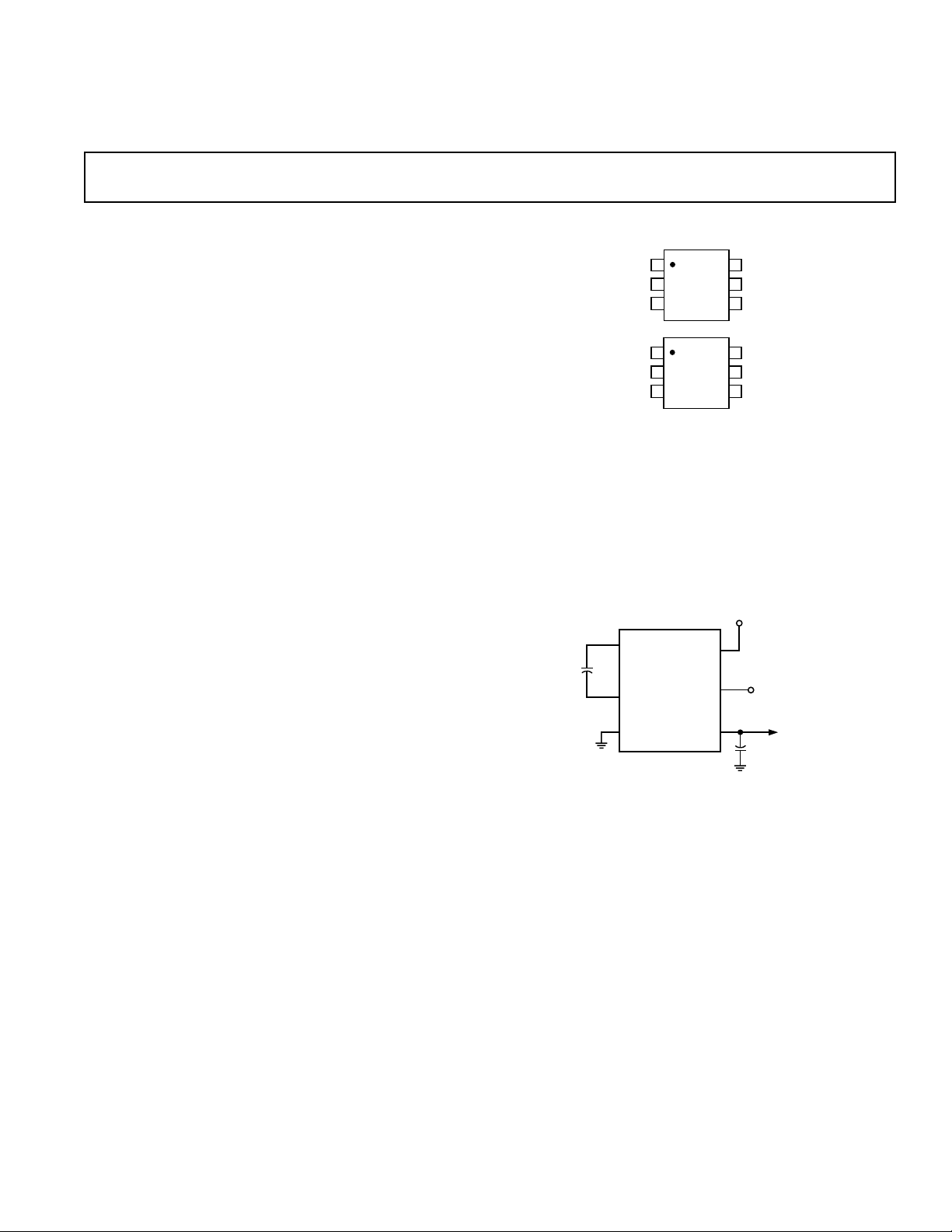
FUNCTIONAL BLOCK DIAGRAMS
1
OUT
2
IN
3
CAP–
1
OUT
2
IN
3
CAP–
NC = NO CONNECT
ADM8828
TOP VIEW
(Not to Scale)
ADM8829
TOP VIEW
(Not to Scale)
6
CAP+
5
SHDN
4
GND
6
CAP+
5
NC
4
GND
GENERAL DESCRIPTION
The ADM8828/ADM8829 is a charge-pump voltage inverter
which may be used to generate a negative supply from a positive
input. Input voltages ranging from +1.5 V to +5.5 V can be
inverted into a negative –1.5 V to –5.5 V output supply. This
inverting scheme is ideal for generating a negative rail in single
power-supply systems. Only two small external capacitors are
needed for the charge pump. Output currents up to 25 mA with
greater than 99% efficiency are achievable.
The ADM8828 also features a low power shutdown (SHDN)
pin. This can be used to disable the device and reduce the quiescent current to 20 nA.
The ADM8828/ADM8829 is available in a 6-lead SOT-23
package.
+1.5V TO +5.5V
INPUT
1mF
CAP+
+
C1
CAP–
GND
ADM8828/
ADM8829
SHDN
OUT
IN
SHUTDOWN
CONTROL
INVERTED
NEGATIVE
OUTPUT
C2
+
1mF
Figure 1. Typical Circuit Configuration
REV. A
Information furnished by Analog Devices is believed to be accurate and
reliable. However, no responsibility is assumed by Analog Devices for its
use, nor for any infringements of patents or other rights of third parties
which may result from its use. No license is granted by implication or
otherwise under any patent or patent rights of Analog Devices.
One Technology Way, P.O. Box 9106, Norwood, MA 02062-9106, U.S.A.
Tel: 781/329-4700 World Wide Web Site: http://www.analog.com
Fax: 781/326-8703 © Analog Devices, Inc., 1999
Page 2
ADM8828/ADM8829–SPECIFICATIONS
(VIN = +5 V, C1, C2 = 1 mF,1 TA = T
wise noted)
MIN
to T
MAX
unless other-
Parameter Min Typ Max Units Test Conditions/Comments
Input Voltage, IN 1.5 5.5 V R
= 10 kΩ
L
Supply Current 600 1000 µA Unloaded
Output Current 25 mA
Output Resistance 18 28 Ω I
Output Ripple 25 mV p-p I
= 5 mA
L
= 5 mA
L
130 mV p-p IL = 25 mA
Charge-Pump Frequency 50 120 190 kHz
65 kHz VIN = +2.25 V
Power Efficiency 90 % R
87 % R
= 200 Ω
L
= 1 kΩ
L
Voltage Conversion Efficiency 99.5 99.96 % No Load
Shutdown Supply Current, I
Shutdown Input Voltage, V
SHDN
SHDN
98 % R
91 % R
0.02 2 µA SHDN = IN
2.0 V SHDN High = Disabled
= 1 kΩ
L
= 200 Ω
L
0.8 V SHDN Low = Enabled
Shutdown Exit Time 175 µsI
NOTES
1
C1 and C2 are low ESR (<0.2 Ω) electrolytic capacitors. High ESR will degrade performance.
Specifications subject to change without notice.
= 5 mA
L
ABSOLUTE MAXIMUM RATINGS*
(T
= +25°C unless otherwise noted)
A
Input Voltage (IN to GND) . . . . . . . . . . . . . . . –0.3 V to +6 V
OUT to GND . . . . . . . . . . . . . . . . . . . . . . . . –6.0 V to +0.3 V
OUT, IN Output Current (Continuous) . . . . . . . . . . . . 50 mA
Output Short Circuit Duration to GND . . . . . . . . . . . 10 secs
Power Dissipation, RT-6 . . . . . . . . . . . . . . . . . . . . . . 570 mW
(Derate 8.3 mW/°C above +70°C)
θ
, Thermal Impedance . . . . . . . . . . . . . . . . . . . . 120°C/W
JA
Operating Temperature Range
Industrial (A Version) . . . . . . . . . . . . . . . . – 40°C to +85°C
Storage Temperature Range . . . . . . . . . . . –65°C to +150°C
Lead Temperature Range (Soldering 10 sec) . . . . . . . . +300°C
Vapor Phase (70 sec) . . . . . . . . . . . . . . . . . . . . . . . . +215°C
Infrared (15 sec) . . . . . . . . . . . . . . . . . . . . . . . . . . . . +220°C
ESD Rating . . . . . . . . . . . . . . . . . . . . . . . . . . . . . . . . >3500 V
*This is a stress rating only and functional operation of the device at these or any
other conditions above those indicated in the operation section of this specification
is not implied. Exposure to absolute maximum rating conditions for extended
periods may affect device reliability.
ORDERING GUIDE
Temperature Branding Package
Model Range Information Option*
ADM8828ART –40°C to +85°C MM0 RT-6
ADM8829ART –40°C to +85°C MN0 RT-6
*RT-6 = 6-lead SOT-23.
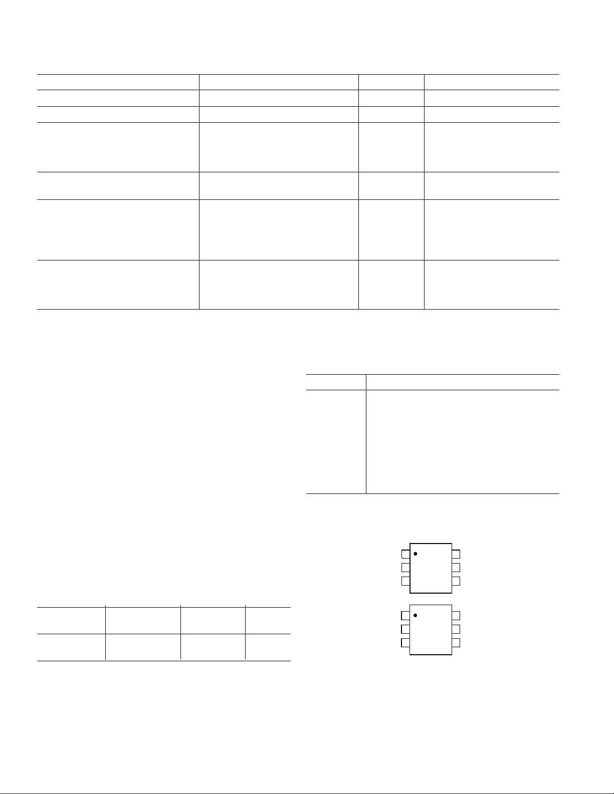
PIN FUNCTION DESCRIPTIONS
Mnemonic Function
CAP+ Positive Charge-Pump Capacitor Terminal.
GND Power Supply Ground.
CAP– Negative Charge-Pump Capacitor Terminal.
OUT Output, Negative Voltage.
SHDN Shutdown Control Input. This input, when
high, is used to disable the charge pump
thereby reducing the power consumption.
IN Positive Power Supply Input.
PIN CONFIGURATIONS
1
OUT
2
IN
(Not to Scale)
3
CAP–
1
OUT
IN
2
(Not to Scale)
3
CAP–
NC = NO CONNECT
ADM8828
TOP VIEW
ADM8829
TOP VIEW
6
5
4
6
5
4
CAP+
SHDN
GND
CAP+
NC
GND
–2–
REV. A
Page 3

Typical Performance Characteristics–
CAPACITANCE – mF
60
50
0
0.47 3.31
OUTPUT VOLTAGE RIPPLE – mV p-p
2.2
40
30
20
10
OUTPUT VOLTAGE RIPPLE
@ V
IN
= 4.75V
OUTPUT VOLTAGE RIPPLE
@ V
IN
= 3.15V
OUTPUT VOLTAGE RIPPLE
@ V
IN
= 1.9V
IL = 5mA
CAPACITANCE – mF
350
300
0
0.47 3.31
OUTPUT VOLTAGE RIPPLE – mV p-p
2.2
200
150
100
50
250
OUTPUT VOLTAGE RIPPLE
@ V
IN
= 1.9V, V
OUT
= –1.5V
OUTPUT VOLTAGE RIPPLE
@ V
IN
= 4.75V, V
OUT
= –4.0V
OUTPUT VOLTAGE RIPPLE
@ V
IN
= 3.15V, V
OUT
= –2.5V
0.8
0.7
0.6
0.5
0.4
0.3
SUPPLY CURRENT – mA
0.2
0.1
0
1 5.51.5
Figure 2. Power Supply Current vs. Voltage
35
30
25
2 2.5 3 3.5 4 4.5 5
SUPPLY VOLTAGE – V
ADM8828/ADM8829
Figure 5. Output Voltage Ripple vs. Capacitance
20
15
10
OUTPUT RESISTANCE – V
5
0
1.5 5.52
Figure 3. Output Source Resistance vs. Supply Voltage
20
18
16
14
12
10
8
6
OUTPUT CURRENT – mA
4
2
0
0.47 3.31
Figure 4. Output Current vs. Capacitance
2.5 3 3.5 4 4.5 5
SUPPLY VOLTAGE – V
OUTPUT CURRENT @ VIN = 4.75V
OUTPUT CURRENT @ VIN = 3.15V
OUTPUT CURRENT @ VIN = 1.9V
CAPACITANCE – mF
2.2
Figure 6. Output Voltage Ripple vs. Capacitance
0
–0.5
–1
–1.5
–2
–2.5
–3
–3.5
OUTPUT VOLTAGE – V
–4
–4.5
–5
0
OUTPUT VOLTAGE @ VIN = 2.0V
OUTPUT VOLTAGE @ VIN = 3.3V
OUTPUT VOLTAGE @ VIN = 5.0V
10 15 20 25 30 35 40
OUTPUT CURRENT – mA
455
Figure 7. Output Voltage vs. Output Current
–3–REV. A
Page 4

ADM8828/ADM8829
100
– %
EFF
P
90
80
70
60
50
40
30
20
10
0
0
P
EFF
10 15 20 25 30 35 40 45
P
EFF
@ VIN = 2.0V
I
– mA
@ VIN = 5.0V
P
@ VIN = 3.3V
EFF
505
Figure 8. Power Efficiency vs. Output Current
50
45
40
35
30
25
20
15
OUTPUT RESISTANCE – V
10
5
0
–50 125–30
RESISTANCE (V) @ VIN = 1.5V
RESISTANCE (V) @ VIN = 3.3V
RESISTANCE (V) @ VIN = 5.0V
–10 10 25 40 60 80 90 110
TEMPERATURE – 8C
Figure 9. Output Resistance vs. Temperature
200
180
160
140
120
100
80
60
PUMP FREQUENCY – kHz
40
20
0
–50 125–30
PUMP FREQUENCY
= 3.3V
@ V
IN
PUMP FREQUENCY
= 5.0V
@ V
IN
PUMP FREQUENCY
@ V
= 1.5V
IN
–10 10 25 40 60 80 90 110
TEMPERATURE – 8C
Figure 10. Charge Pump Frequency vs. Temperature
–4–
REV. A
Page 5

ADM8828/ADM8829
GENERAL INFORMATION
The ADM8828/ADM8829 is a switched capacitor voltage converter that can be used to invert the input supply voltage.
The voltage conversion task is achieved using a switched capacitor technique using two external charge storage capacitors. An
on-chip oscillator and switching network transfers charge between
the charge storage capacitors. The basic principle behind the
voltage conversion scheme is illustrated below.
S1
V+
S2
CAP+
S3
+
C1
S4
CAP–
F1 F2
4 2
OSCILLATOR
+
OUT = –V+
C2
Figure 11. Voltage Inversion Principle
An oscillator generating antiphase signals φ1 and φ2 controls
switches S1, S2 and S3, S4. During φ1, switches S1 and S2 are
closed while S3 and S4 are open, thereby charging C1 up to the
voltage at V+. During φ2, S1 and S2 open and S3 and S4 close.
The positive terminal of C1 is connected to GND via S3 during
this phase and the negative terminal of C1 connects to V
via S4. The net result is voltage inversion at V
OUT
OUT
wrt GND.
Charge on C1 is transferred to C2 during φ2. Capacitor C2
maintains this voltage during φ1. The charge transfer efficiency
depends on the on-resistance of the switches, the frequency at
which they are being switched and also on the equivalent series
resistance (ESR) of the external capacitors. For maximum efficiency, capacitors with low ESR are, therefore, recommended.
Shutdown Input
The ADM8828 contains a shutdown input that can be used to
disable the device and hence reduce the power consumption. A
logic high level on the SHDN input shuts the device down
reducing the quiescent current to 0.02 µA. During shutdown
the output voltage discharges to 0 V. Therefore, ground referenced loads are not powered during this state. When exiting
shutdown, it takes several cycles (approximately 175 µs) for the
charge pump to reach its final value. If the shutdown function is
not being used, SHDN should be hardwired to GND.
Capacitor Selection
The flying capacitor C1 can be increased to reduce the output
resistance.
The output capacitor size C2 affects the output ripple. Increasing the capacitor size reduces the peak-peak ripple. The ESR
affects both the output impedance and the output ripple.
Reducing the ESR reduces the output impedance and ripple.
For convenience it is recommended that both C1 and C2 be the
same value.
The ac impedance of the ADM8828/ADM8829 may be reduced
by using a bypass capacitor on the input supply. This capacitor
should be connected between the input supply and GND. It will
provide instantaneous current surges as required. Suitable capaci-
tors of 1 µF or greater may be used.
+1.5V TO +5.5V
INPUT
1mF
CAP+
+
C1
CAP–
GND
ADM8828/
ADM8829
SHDN
OUT
IN
SHUTDOWN
CONTROL
INVERTED
NEGATIVE
OUTPUT
C2
+
1mF
Figure 12. Typical Circuit Configuration
–5–REV. A
Page 6

ADM8828/ADM8829
OUTLINE DIMENSIONS
Dimensions shown in inches and (mm).
6-Lead SOT-23
(RT-6)
0.122 (3.10)
0.106 (2.70)
0.071 (1.80)
0.059 (1.50)
0.051 (1.30)
0.035 (0.90)
PIN 1
0.006 (0.15)
0.000 (0.00)
1
0.075 (1.90)
2
BSC
0.020 (0.50)
0.010 (0.25)
4 5 6
0.118 (3.00)
0.098 (2.50)
3
0.037 (0.95) BSC
0.057 (1.45)
0.035 (0.90)
SEATING
PLANE
0.009 (0.23)
0.003 (0.08)
108
08
C3352a–0–10/99
0.022 (0.55)
0.014 (0.35)
–6–
PRINTED IN U.S.A.
REV. A
 Loading...