

Page 1

A
ADM8211
IEEE802.11b WLAN NIC Solution
PCI/miniPCI/Cardbus Interface w i th M AC Unit +
Baseband Processor (BBP)
DATASHEET
Rev. 1.1
Feb, 2003
Information in this document is provided in connection with ADMtek products. ADMtek may make changes to
specifications and product descriptions at any time, without notice. Designers must not rely on the absence or
characteristics of any features or instructions marked "reserved" or "undefined." ADMtek reserves these for future
definition and shall have no responsibility whatsoever for conflicts or incompatibilities arising from future changes to
them.
The products may contain design defects or errors known as errata, which may cause the product to deviate from
published specifications. Current characterized errata are available on request. To obtain latest documents, please contact
your local ADMtek sales office or your distributor or visit ADMtek’s website at http://www.ADMtek.com.tw
*Third-party brands and names are the property of their respective owners.
DMtek
Partnership Now & Future
1
Page 2

A
REVISION HISTORY
Revision Date Revision Description
Mar, 2002 0.1 Draft
Apr, 2002 0.3 Preliminary version
Apr, 2002 0.4 Change EEPROM format
Rename GPIO0
May, 2002 0.5 Rename EEPROM [54:60] as Tx Power
May, 2002 0.6 Add missed pins in Pin Description, C1, C2, D1, D2
Oct, 2002 0.7 Remove unnecessary chapters
Update EEPROM format
Nov, 2002 0.8 Remove PWRLEDACT
Remove GPIO2
Feb, 2003 1.0 Formal release
Mar, 2003 1.1 Correct Chapter 6, Electrical Specifications
DMtek
Partnership Now & Future
2
Page 3

A
Content
1 GENERAL DESCRIPTION.................................................................5
2 FEATURES ............................................................................................6
2.1 HOST PCI INTERFACE.....................................................................................................................6
2.2 INDUSTRY STANDARD ......................................................................................................................6
2.3 802.11 MAC....................................................................................................................................6
2.4 WEP................................................................................................................................................6
2.5 WLAN TX/RX FIFO.....................................................................................................................7
2.6 WLAN SYNTHESIZER INTERFACE .................................................................................................7
2.7 EEPROM INTERFACE....................................................................................................................7
2.8 LED DISPLAY..................................................................................................................................7
2.9 MISCELLANEOUS.............................................................................................................................7
3 APPLICATION DIAGRAM.................................................................8
4 PIN ASSIGNMENT DIAGRAM..........................................................9
5 PIN DESCRIPTION............................................................................10
5.1 PCI INTERFACE.............................................................................................................................10
5.2 EEPROM INTERFACE..................................................................................................................11
5.3 SERIAL INTERF A CE TO SYNTHESIZER ..........................................................................................12
5.4 RF I/F............................................................................................................................................12
5.5 LED DISPLAY, GPIO.....................................................................................................................12
5.6 MISCELLANEOUS...........................................................................................................................13
5.7 ON CHIP REGULATOR PINS............................................................................................................13
5.8 DIGITAL POWER PINS ...................................................................................................................13
5.9 ANALOG POWER PINS...................................................................................................................13
DMtek
Partnership Now & Future
3
Page 4

A
5.10 CLOCK PINS ............................................................................................................................... ...13
6 ELECTRICAL SPE C IFICATIONS AND TIMINGS......................14
6.1 ABSOLUTE MAXIMUM RATINGS ...................................................................................................14
6.2 OPERATING CONDITION................................................................................................................14
6.3 DC SPECIFICATIONS .....................................................................................................................14
6.4 EEPROM INTERFACE DC SPECIFICATION..................................................................................14
6.5 GPIO INTERFACE DC SPECIFICATION ........................................................................................15
6.6 RESET TIMING...............................................................................................................................15
6.7 EEPROM INTERFACE TIMING SPECIFICATION..........................................................................15
7 PACKAGE............................................................................................17
DMtek
Partnership Now & Future
4
Page 5
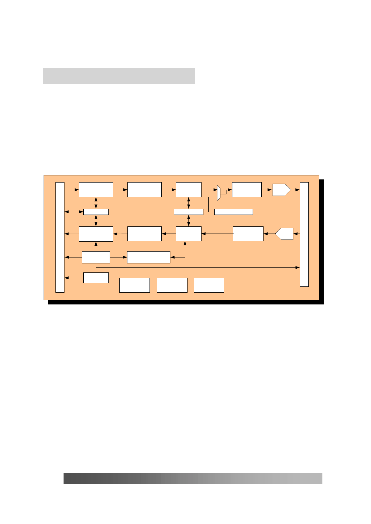
11
Tx MAC
Rx MAC
Modulator
Preamble/Header
Demodulator ADC
DAC
GGeenneerraall DDeessccrriippttiioonn
ADM8211 is a high performance PCI/miniPCI/Cardbus single chip with WLAN MAC cont roller and
Baseband processor integrated.
ADMtek is the leading of networking SOC, based on mature experience, ADM8211 is designed as
hardwired architecture to reach the cost eff ective target.
With the features of SRAM-needless, power saving, WEP/f ix, small-package…etc. ADM8211 is
versatile for W LAN system manuf acturers to develop IEEE 802.11b wireless product.
Tx Buffer
Management
Arbiter WEP Engine
PCI/IF Control
Rx Buffer
Management
WLAN CSR
Tx FIFO
Rx FIFO
Magic Pkt / Wake-up
Frame
Synthesizer, RF I/F
WLAN CR
EEPROM I/F LED/GPIO Clock Gen
ADMtek
Partnership Now & Future
5
Page 6

2
2
FFeeaattuurreess
2.1 Host PCI interface
Provides 32-bit PCI bus master data transfer
Supports network operation with PCI system clock from 22 MHz to 33MHz
Provides performance meter, PCI bus master latency timer, for tuning the threshold to
enhance the performance
Provides burst-transmit packet interrupt and transmit/receive early interrupt to reduce host
CPU utilization.
Supports memory-read, memory-read-line, memory-read-multiple, memory-write,
memory-write-and-invalidate command while being bus master
Supports big or little endian byt e ordering
Arbitration between DMA channel to minimize underflow or overflow
2.2 Industry standard
PCI 2.2 /Cardbus interface
ACPI and PCI power management 1.1 standard compliant
IEEE802.11, IEEE802.11b
2.3 802.11 MAC
MAC implement s with State Machine
No External SRAM needed
Support auto-fallback from 11Mbps to 5. 5, 2 and 1Mbps.
Support Infrastructure, Ad-hoc under Dist ributed Coordination Function (DCF)
Implementation the Point Coordination Function (PCF) operation
RTS/CTS generation, Fragmentation, Beacon monitor/loss detection/generation.
RX DA address filtering (multicast) with 64 entries.
TIM (Traffic Indication Map) field decoding at Beacon frame reception
Support DSSS (Direct Sequence Spread Spectrum) PHY.
Front end chip power s equence contr ol
2.4 WEP
Internal encryption engine for WEP function, RC4, 40/104 bits k ey length selectable.
ADMtek
Partnership Now & Future
6
Page 7

Randomly generated IV ( I nit ialization Vector) for TX.
ICV (Integrity Check Value) generation and check.
4 default shared key supported.
TA/RA WEP individual key management with a 20-entry table.
2.5 WLAN TX/RX FIFO
Provides two independent long FIFOs with 4k bytes each for transmission and receiving
Bus master descriptor based host memory access
Pre-fetch up to two transmit packets to guarantee standard inter frame spac e (I FS)
Re-transmits no-ACKed packet without reloading from host memory.
Support two TX descriptors for DCF and PCF application
Automatically re-t rans mit t ing if T X under-run happened.
2.6 WLAN Synthesizer Interface
Support RFMD compatible interface
2.7 EEPROM Interface
Provides serial interface for read/write 93C46/93C66 EEPROM
Automatically loads device I D, vendor ID, subsystem ID, subsystem vendor ID,
Maximum-Latency, and Minimum-Grand from the 64 byte contents of 93C46/93C66 aft er
PCI reset de-asserted in PCI environment.
CIS data is recalled from 93C66 through ADM8211 in CARDBUS environment.
2.8 LED Display
Power: Power on indication
Link: Keep on while link
Activity: Blinking at 10Hz while activity
2.9 Miscellaneous
Low power application
Support 3 GPIO pins
CMOS .25um Process
Provides 156/BGA package
On chip 3. 3V ~ 2.5V regulator
3.3V power supply with 5V/3.3V I/O tolerance
ADMtek
Partnership Now & Future
7
Page 8

3
3
AApppplliiccaattiioonn DDiiaaggrraam
* Please refer to schematic provided by ADMtek
EEPROM
ADM8211
MAC+BBP
PCI / miniPCI / Cardbus Interface
m
RF
SAW
PA
44M Hz
Crystal
LEDs
ADMtek
Partnership Now & Future
8
Page 9

4
4
PPiinn AAssssiiggnnm
meenntt DDiiaaggrraa
1413121110987654321
Bottom View
156-Pin BGA
m
m
A1 Ball Pad Corner
A
B
C
D
E
F
G
H
J
K
L
M
N
P
1 2 3 4 5 6 7 8 9 10 11 12 13 14
A VSS PA_PE PE1 PE2 VD33 EECS EEDI LEDACT
B VDDA GNDA LE_IF# SYNDATA SYNCLK VD33 VD33 EECK EEDO VSSPST
C Q_in I_in RXVGC MCLK LEDLINK OSC44O CLK_44
D Q_out I_out TXVGC LNA_GS GNDD VDDD VSSPST VSSPST OSC44I GPIO3
E VREF ANTSEL VSSPST BW_SEL VSSPST VSSPST
F VDDA GNDA VD33 VSSPST GPIO1
G VSS INTA# VSS VSSPST VSENSE VSA VCTL VDDAH
H REQ# PCI-CLK VD33 VD33 VSSPST VAUX3.3 AD0
J AD31
K GNT# VSSPST VSSPST RST# AD5 AD3 VSSPST VD33
L AD28 AD29 AD30 AD17 AD26 AD20 AD25 DEVSEL# AD16 AD9 AD12 AD11 AD4 AD6
M VDD FRAME# VDD VDD AD27 VD33 VSSPST AD13 PERR# STOP# AD15 VSS AD8 C-BEB0
N AD24 C-BEB3 AD22 VDD C-BEB2 VSS AD18 SERR# VSS VD33 PAR VSS AD14 AD7
P IDSEL AD23 AD19 AD21 IRDY# TRDY# VSSPST VSSPST PCI/CB VD33 C-BEB1 AD10
PME#/
CSTSCHG
VDD VD33 AD2 AD1 VCC_DETECT CLKRUN
ADMtek
Partnership Now & Future
9
Page 10

5
5
PPiinn DDeessccrriippttiioonn
5.1 PCI Interface
Pin Name Type Description
G2 INTA# O/D PCI interrupt acknowledge.
K4 RST# I
H2 PCI-CLK I This PCI clock inputs to ADM8211. The bus signals are recognized on
K1 GNT# I This signal indicates that the bus request of ADM8211 have been
H1 REQ# O Bus master device request.
J2 PME# /
CSTSCHG
J1
AD31
L3
AD30
L2
AD29
L1
AD28
M5
AD27
L5
AD26
L7
AD25
N1
AD24
P3
AD23
N3
AD22
P5
AD21
L6
AD20
P4
AD19
N8
AD18
L4
AD17
L9
AD16
M11
AD15
N13
AD14
M8
AD13
L11
AD12
M12
AD11
P13
AD10
I/O The Power Management Event signal is an open drain, active low
I/O Multiplexed address data pin of PCI Bus
PCI reset signal, at least 100µs. During the reset period, all the
output pins of ADM8211 wi ll be set to tri-state and a ll the O/D pins
are floated.
rising edge of PCI-CLK. The frequency range of PCI-CLK is limited
between 20MHz and 33MHz.
accepted.
signal for PCI (PME#)
When CSR18.bit19 is set into “1”, means that the ADM8211 is set
into Power Save mode. In this mode, when the ADM821 1 receives a
Beacon (TIM) or ATIM frame from network then the ADM8211 will
active this signal too.
ADMtek
Partnership Now & Future
10
Page 11

L10
AD9
M13
AD8
N14
AD7
L14
AD6
K11
AD5
L13
AD4
K12
AD3
J11
AD2
J12
AD1
H14
AD0
N2
C-BEB3
N5
C-BEB2
P12
C-BEB1
M14
C-BEB0
P2 IDSEL I Initialization Device Select. This signal is asserted when host issues
M2 FRAME# I/O Begin and duration of bus access, driven by master device
P6 IRDY# I/O Master device is ready to data transaction
P7 TRDY# I/O Slave device is ready to data transaction
L8 DEVSEL# I/O Device select, target is driving to indicate the address is decoded
M10 STOP# I/O Target device request the master device to stop the current
M9 PERR# I/O Data parity error is detected, driven by the agent receiving data
N8 SERR# O/D Address parity error
N11 PAR I/O Parity, even parity (AD[31:0] + C/BE[3:0]), master drives par for
J14 CLKRUN I/O
P10 PCI/CB I Bonding low to select CARD bus mode.
I/O Bus command and byte enable
the configuration cycles to the ADM8211.
transaction
address and write data phase, target drives par for read data phase
Clock Run for PCI system. In the normal operation situation, Host
O/D
should assert this signal to indicate ADM8211 about the normal
situation. On the other hand, when Host will deassert this signal
when the clock is going down to a nonoperating frequency. When
ADM8211 recognizes the deasserted status of clk-run, then it will
assert clk-run to request host to maintain the normal clock
operation. When clk-ru n function is disabled then the ADM8 211 will
set clk-run in tri-state.
Internal pull up. 5V-tolerant
5.2 EEPROM Interface
Pin Name Type Description
B11 EECK I /O ECK: Clock output to serial EEPROM.
A12 EEDI I/O EDI: Data output to serial EEPROM.
ADMtek
Partnership Now & Future
pull-up, 5V tolerant
pull-up, 5V tolerant
11
Page 12

B12 EEDO I/O EDO: Data input from serial EEPROM
pull-up, 5V tolerant
A11 EECS O Chip Select of serial EEPROM
Pull-down, 5V tolerant
5.3 Serial Interface to Synthesizer
Pin Name Type Description
B5 LEIF# O, pull-up Synthesizer 2 Chip Select
B7 SYNCLK O, pull-up Clock
B6 SYNDATA O, pull-up Data
5.4 RF I/F
Pin Name Type Description
A8 PE1 O, pull-up Power enable 1
A9 PE2 O, pull-up Power enable 2
E12 BW_SEL O Channel 14 control pin
A7 PA_PE O, pull-up Transmit PA Power Enable
C1 Q_in I Analog Q input
D1 Q_out O Analog Q output 1.6V-1.8V
C2 I_in I Analog I input
D2 I_out O Analog I output 1.6V-1.8V
5.5 LED display, GPIO
Pin Name Type Description
C12 LEDLINK O, pull-up
A13 LEDACT O, pull-up
F12
GPIO1 I/O
D14
GPIO3 I/O
LED Drive.
10 Hz blinking while either of following 2 conditions
effective, even at D3-Cold.
(1) Association successful with AP
(2) Beacon reception when join IBSS
LED Drive.
10 Hz blinking while TX/RX Frame is detected
General-purpose I/O pins, refer to GPIOEN setting (CSR11A).
Pull-up, 5V tolerant
General-purpose I/O pins, capable of event, rise/fall edge
or toggle, capturing to generate interrupt to host, if
enabled.
Pull-up, 5V tolerant
ADMtek
Partnership Now & Future
12
Page 13

5.6 Miscellaneous
Pin Name Type Description
H13 Vaux3.3 I, Schmmit
5V tolerant
J13 VDD_detect I, Schmmit
5V tolerant
5.7 On chip regulator Pins
Pin Name Type Description
G13 REGCTL I/O Regulator control pin
G12 VSA Power GND for regulator
G14 VDDAH Power 3.3V for regulator
G11 VSENSE I 2.5V sense input
When asserted, it indicates an auxiliary power source is
supported
ACPI purpose, for detecting the auxiliary power source.
When asserted, it indicates PCI power source is supported .
ACPI purpose, for detecting the main power is remained or
not, this pin should be connected to PCI bus power sour ce
+3.3V.
5.8 Digital Power Pins
Pin Name Type Description
F4, H4, J4, M 6, B9, A10, B10, H11, N1 0, P11,
J14
K2, K3, G4, M7, P8, P9, D11, E11, F11, D12,
H12, E13, K13, B14, E14
G1, M1, J1, M3, M4, N4, M12, N12 VDD Power 2.5V for core
A2, G3, N6, N9, VSS Power Gnd for core
D8 VDDD Power Vcc for BBP (leave open)
D7 GNDD Power Gnd for BBP
5.9 Analog Power Pins
Pin Name Type Description
B1, F2 VDDA Power 3.0V for BBP
B2, F3 GNDA Power Analog Gnd for BBP
5.10 Clock Pins
Pin Name Type Description
A13 OSC44I I 44 MHz clock input
C13 OSC44O O 44 MHz clock output
C14 CLK 44 O, pull-up Buffered 44Mhz clock output
VDD33 Power 3.3V for IO
VSSPST Power Gnd for IO
This signal will be stopped, forced low, during MAC
enter into power saving mode.
ADMtek
Partnership Now & Future
13
Page 14

6
6
EElleeccttrriiccaall SSppeecciiffiiccaattiioonnss aanndd TTiim
miinnggss
6.1 Absolute Maximum Ratings
Supply Voltage (VDD) -0.3 V to 3.6 V
DC Input Voltage (VIN) -0.5 V to VDD+0.5V
DC Output Voltage (VOUT) -0.5 V to VDD+0.5V
Storage Temperature
Ambient Temperature 0 C to 70 C
ESD Rating
-65 C to 150 C
2000V
6.2 Operating Condition
Symbol Parameter Condition Min Max Units
VDD Supply Voltage 3.0 3.6 V
6.3 DC Specifications
Symbol Parameter Condition Min Max Units
Vih Input High Voltage 2.0 V
Vil Input Low Voltage 0.8 V
Iih Differential Input Sensitivity 0.1 V
V
cm
Voh Output High Voltage 2.8 3.6 V
Vol Output Low Voltage 0.0 0.3 V
V
crs
Differential Common Mode
Range
Output Signal Crossover
Voltage
0.8 2.5 V
0.8 2.5 V
6.4 EEPROM Interface DC specification
Standard Vcc (4.5V to 5.5V) DC Specification
Symbol Parameter Condition Min Max Units
Vih Input H igh Voltage 2.0 Vcc +1 V
Vil Input Low Voltage -0.1 0.8 V
Iih Input High Leakage Current 0<V
I
il
Vol Output Low Voltage
Voh Output High Voltage
Cin Input Pin Capacitance 5 pF
ADMtek
Partnership Now & Future
Input Low Leakage Current 0<V
I
oH
I
oL
< Vcc 1
in
< Vcc -1
in
= -10 µA
= 10 µA
Vcc –0.2 V
0.2 V
µA
µA
14
Page 15

Low Vcc (2.7V to 5.5V) DC Specification
Symbol Parameter Condition Min Max Units
Vih Input H igh Voltage 0.8Vcc V cc +1 V
Vil Input Low Voltage -0.1 0.15Vcc V
Iih Input High Leakage Current 0<V
I
il
Input Low Leakage Current 0<V
Voh Output High Voltage
Vol Output Low Voltage
Cin Input Pin Capacitance 5 pF
6.5 GPIO Interface DC Specification
Symbol Parameter Condition Min Max Units
Vih Input High Voltage 2.0 V
Vil Input Low Voltage 0.8 V
Iih Input High Leakage Current 0<V
I
il
Voh Output High Voltage IoH = -4 mA 2.4 V
Vol Output Low Voltage IoL = 4 mA 0.4 V
Input Low Leakage Current 0<V
< Vcc 1
in
< Vcc -1
in
= -10 µA
I
oH
= 10 µA
I
oL
< Vcc 10
in
< Vcc -10
in
0.9Vcc V
0.1Vcc V
µA
µA
µA
µA
6.6 Reset Timing
ADM8211 can be reset either by hardware, software or USB reset.
A hardware reset is accomplished by asserting the RST# pin after power up the device. It should
have a duration of at least 50 ms to ensure the ex t ernal 48MHz crystal is in stable and correct
frequency. All registers will be res et to default values.
A software reset is accomplished by setting the reset bit. This software reset will reset all registers
to default values.
6.7 EEPROM Interface Timing Specification
Symbol Parameter Min Max Units
t
EESK Clock Frequency 0 1 MHz
EESK
T
EECS Setup Time to EESK 0.2
EECSS
T
EECS Hold Time from EESK 0 ns
EECSH
T
EEDO Hold Time from EESK 70 ns
EEDOH
T
EEDO Output Delay to “1” or “0” 2
EEDOP
µs
µs
ADMtek
Partnership Now & Future
15
Page 16

t
EEDI Setup Time to EESK 0.4
EEDIS
t
EEDI Hold Time from EESK 0.4
EEDIH
µs
µs
ADMtek
Partnership Now & Future
16
Page 17

77
PPaacckkaaggee
Package: 156-pin BGA
Dimension: 15mm*15mm*1.81mm
ADMtek
Partnership Now & Future
17
 Loading...