

Page 1

ADM7008
Octal Ethernet 10/100M PHY
Datasheet
Version 1.0
ADMtek.com.tw
Information in this document is provided in connection with ADMtek products. ADMtek may make
changes to specifications and product descriptions at any time, without notice. Designers must not rely on
the absence or characteristics of any features or instructions marked “reserved” or “undefined”. ADMtek
reserves these for future definition and shall have no responsibility whatsoever for conflicts or
incompatibilities arising from future changes to them
The products may contain design defects or errors know as errata, which may cause the product to deviate
from published specifications. Current characterized errata are available on request. To obtain latest
documentation please contact you local ADMtek sales office or visit ADMtek’s website at
http://www.ADMtek.com.tw
*Third-party brands and names are the property of their respective owners.
Copyright 2003 by ADMtek Incorporated All Rights Reserved
Page 2

ADMtek Inc. V1.0
About this Manual
Intended Audience
Structure
This Data sheet contains 6 chapters
Chapter 1 Product Overview
Chapter 2 Interface Description
Chapter 3 Function Description
Chapter 4. Register Description
Chapter 5. Electrical Specification
Chapter 6. Packaging
Revision History
Date Version Change
23 January 2003
1.0 First release of ADM7008
Customer Support
ADMtek Incorporated,
2F, No.2, Li-Hsin Rd.,
Science-based Industrial Park,
Hsinchu, 300, Taiwan, R.O.C.
Sales Information
Tel + 886-3-5788879
Fax + 886-3-5788871
ADM7008
Page 3

ADMtek Inc. V1.0
Table of Contents
Chapter 1 Product Overview ........................................................................................ 1-1
1.1 Overview.......................................................................................................... 1-1
1.2 Features............................................................................................................1-2
1.3 Block Diagram.................................................................................................1-3
1.4 Abbreviations...................................................................................................1-3
1.5 Conventions ..................................................................................................... 1-5
1.5.1 Data Lengths............................................................................................ 1-5
1.5.2 Register Type Descriptions...................................................................... 1-5
1.5.3 Pin Type Descriptions.............................................................................. 1-5
Chapter 2 Interface Description................................................................................... 2-1
2.1 Pin Diagram ..................................................................................................... 2-1
2.2 Pin Description................................................................................................. 2-2
2.2.1 Twisted Pair Interface, 32 pins................................................................ 2-2
2.2.2 Ground and Power, 20 pins..................................................................... 2-2
2.2.3 Mode Setting ............................................................................................2-2
2.2.4 Clock Input Select .................................................................................... 2-2
2.2.5 Clock Input, 3 pins ................................................................................... 2-3
2.2.6 RMII/SMII Interface, 48 pins................................................................... 2-3
2.2.7 ATPG Signals, 2 pins ............................................................................. 2-16
2.2.8 Reset Pin ................................................................................................ 2-16
2.2.9 Control Signals, 3 pins........................................................................... 2-16
2.2.10 LED Interface, 2 pins............................................................................. 2-17
2.2.11 Regulator Control, 2 pins ......................................................................2-17
2.2.12 Digital Power/Ground, 13 pins.............................................................. 2-17
Chapter 3 Function Description ................................................................................... 3-1
3.1 10/100M PHY Block .......................................................................................3-2
3.1.1 100Base-X Module................................................................................... 3-2
3.1.2 100Base-TX Receiver............................................................................... 3-2
3.1.3 100Base-TX Transmitter.......................................................................... 3-7
3.1.4 100Base-FX Receiver............................................................................... 3-7
3.1.5 100Base-FX Transmitter.......................................................................... 3-8
3.1.6 10Base-T Module..................................................................................... 3-8
3.1.7 Operation Modes .....................................................................................3-8
3.1.8 Manchester Encoder/Decoder ................................................................. 3-8
3.1.9 Transmit Driver and Receiver .................................................................3-9
3.1.10 Smart Squelch ..........................................................................................3-9
3.1.11 Carrier Sense ........................................................................................... 3-9
3.1.12 Collision Detection ................................................................................ 3-10
3.1.13 Jabber Function..................................................................................... 3-10
3.1.14 Link Test Function ................................................................................. 3-10
3.1.15 Automatic Link Polarity Detection ........................................................ 3-11
3.1.16 Clock Synthesizer................................................................................... 3-11
3.1.17 Cable Broken Auto Detection ................................................................3-11
3.1.18 Auto Negotiation .................................................................................... 3-12
3.1.19 Auto Negotiation and Speed Configuration........................................... 3-13
ADM7008 i
Page 4

ADMtek Inc. V1.0
3.2 MAC Interface ............................................................................................... 3-13
3.2.1 Reduced Media Independent Interface (RMII) ...................................... 3-14
3.2.2 Receive Path for 100M........................................................................... 3-14
3.2.3 Receive Path for 10M............................................................................. 3-16
3.2.4 Transmit Path for 100M ........................................................................ 3-16
3.2.5 Transmit Path for 10M .......................................................................... 3-16
3.2.6 Serial and Source Synchronous Media Independent Interface.............. 3-17
3.2.7 100M Receive Path ................................................................................ 3-18
3.2.8 10M Receive Path .................................................................................. 3-19
3.2.9 100M Transmit Path .............................................................................. 3-20
3.2.10 10M Transmit Path ................................................................................ 3-20
3.3 LED Display ..................................................................................................3-21
3.3.1 Single Color LED................................................................................... 3-21
3.3.2 Dual Color LED..................................................................................... 3-23
3.3.3 Serial Output LED Status ...................................................................... 3-23
3.3.4 RMII Mode (RSMODE1 = 1)................................................................. 3-24
3.3.5 SMII/SS_SMII Mode (RSMODE1 = 0).................................................. 3-24
3.4 Management Register Access........................................................................ 3-24
3.4.1 Preamble Suppression ...........................................................................3-25
3.4.2 Reset Operation .....................................................................................3-25
3.5 Power Management .......................................................................................3-26
3.5.1 Medium Detect Power Saving................................................................ 3-26
3.5.2 Transmit Power Saving.......................................................................... 3-27
3.6 Voltage Regulator .......................................................................................... 3-28
Chapter 4 Register Description .................................................................................... 4-1
4.1 Register Mapping.............................................................................................4-1
4.2 Register Bit Mapping....................................................................................... 4-2
4.2.1 Register #0h -- Control Register.............................................................. 4-2
4.2.2 Register #1h – Status Register ................................................................. 4-2
4.2.3 Register #2h – PHY ID Register (002E) .................................................. 4-2
4.2.4 Register #3h – PHY ID Register (CC11) ................................................. 4-2
4.2.5 Register #4h – Advertisement Register .................................................... 4-2
4.2.6 Register #5h – Link Partner Ability Register........................................... 4-2
4.2.7 Register #6h – Auto Negotiation Expansion Register.............................. 4-2
4.2.8 Register #7h – # Fh Reserved .................................................................. 4-2
4.2.9 Register #10h – PHY Configuration Register.......................................... 4-2
4.2.10 Register #11h – 10M Configuration Register.......................................... 4-3
4.2.11 Register #12h – 100M Configuration Register........................................ 4-3
4.2.12 Register #13h – LED Configuration Register.......................................... 4-3
4.2.13 Register #14h – Interrupt Enable Register .............................................. 4-3
4.2.14 Register #16h – PHY Generic Status Register......................................... 4-3
4.2.15 Register #17h – PHY Specific Status Register......................................... 4-3
4.2.16 Register #18h – Recommend Value Storage Register ............................. 4-3
4.2.17 Register #19h – Interrupt Status Register................................................ 4-3
4.2.18 Register #1dh – Receive Error Counter .................................................. 4-4
4.2.19 Register #1eh – Chip ID (8888
) ............................................................... 4-4
ADM7008 ii
Page 5

ADMtek Inc. V1.0
4.2.20 Register #1fh –Total Interrupt Status (only For Port 0).......................... 4-4
4.3 Register Description......................................................................................... 4-4
4.3.1 Control (Register 0h) ............................................................................... 4-4
4.3.2 Status (Register 1h).................................................................................. 4-6
4.3.3 PHY Identifier Register (Register 2h)...................................................... 4-8
4.3.4 PHY Identifier Register (Register 3h)...................................................... 4-8
4.3.5 Advertisement (Register 4h)..................................................................... 4-9
4.3.6 Auto Negotiation Link Partner Ability (Register 5h)............................. 4-10
4.3.7 Auto Negotiation Expansion Register (Register 6h).............................. 4-11
4.3.8 Register Reserved (Register 7h-Fh).......................................................4-11
4.3.9 Generic PHY Configuration Register (Register 10h) ............................ 4-11
4.3.10 PHY 10M Module Configuration Register (Register 11h) ....................4-12
4.3.11 PHY 100M Module Control Register (Register 12h)............................. 4-13
4.3.12 LED Configuration Register (Register 13h).......................................... 4-13
4.3.13 Interrupt Enable Register (Register 14h) ..............................................4-15
4.3.14 PHY Generic Status Register (Register 16h)......................................... 4-16
4.3.15 PHY Specific Status Register (Register 17h) ......................................... 4-17
4.3.16 PHY Recommend Value Status Register (Register 18h)........................ 4-18
4.3.17 Interrupt Status Register (Register 19h)................................................ 4-18
4.3.18 Receive Error Counter Register (Register 1Dh).................................... 4-19
4.3.19 Chip ID Register (Register 1Fh)............................................................4-20
4.3.20 Per port Interrupt and Revision ID Register (Register 1Eh)................. 4-20
Chapter 5 Electrical Specification................................................................................ 5-1
5.1 DC Characterization......................................................................................... 5-1
5.1.1 Absolute Maximum Rating....................................................................... 5-1
5.1.2 Recommended Operating Conditions ...................................................... 5-1
5.1.3 DC Electrical Characteristics for 3.3V Operation.................................. 5-1
5.2 AC Characterization......................................................................................... 5-2
5.2.1 XI/OSCI (Crystal/Oscillator) Timing....................................................... 5-2
5.3 RMII Timing.................................................................................................... 5-3
5.3.1 REFCLK Input Timing (When REFCLK_SEL is set to 1) .......................5-3
5.3.2 REFCLK Output Timing (When REFCLK_SEL is set to 0)..................... 5-4
5.3.3 RMII Transmit Timing .............................................................................5-5
5.3.4 RMII Receive Timing ...............................................................................5-6
5.4 SMII Clock Timing..........................................................................................5-7
5.4.1 REFCLK Input Timing (When REFCLK_SEL is set to 1) -..................... 5-7
5.4.2 REFCLK Output Timing (When REFCLK_SEL is set to 1)..................... 5-8
5.4.3 SMII/SS_SMII Transmit Timing............................................................... 5-9
5.4.4 SMII/SS_SMII Receive Timing............................................................... 5-10
5.5 Serial Management Interface (MDC/MDIO) Timing.................................... 5-11
5.6 Power On Configuration Timing ................................................................... 5-12
Chapter 6 Packaging...................................................................................................... 6-1
ADM7008 iii
Page 6

ADMtek Inc. V1.0
List of Figures
Figure 1-1 ADM7008 Block Diagram.......................................................................................1-3
Figure 2-1 ADM7008 Pin Assignment ......................................................................................2-1
Figure 3-1 ADM7008 Switch Application (10/100M TP Mode) ..................................................... 3-1
Figure 3-2 100Base-X Block Diagram and Data Path................................................................... 3-3
Figure 3-3 10Base-T Block Diagram and Data Path................................................................... 3-10
Figure 3-4 RMII Signal Diagram ...........................................................................................3-14
Figure 3-5 RMII Reception Without Error ...............................................................................3-15
Figure 3-6 RMII Reception with False Carrier (100M Only)........................................................ 3-15
Figure 3-7 RMII Reception with Symbol Error ......................................................................... 3-15
Figure 3-8 10M RMII Receive Diagram .................................................................................. 3-16
Figure 3-9 100M RMII Transmit Diagram ............................................................................... 3-16
Figure 3-10 10M RMII Transmit Diagram ............................................................................... 3-17
Figure 3-11 SMII Signal Diagram .......................................................................................... 3-18
Figure 3-12 SS_SMII Signal Diagram..................................................................................... 3-18
Figure 3-13 100M SMII Receive Timing Diagram .................................................................... 3-18
Figure 3-14 100M SS_SMII Receive Timing Diagram ...............................................................3-18
Figure 3-15 10M SMII Receive Timing Diagram ...................................................................... 3-19
Figure 3-16 10M SS_SMII Receive Timing Diagram................................................................. 3-19
Figure 3-17 100M SMII Transmit Timing Diagram ...................................................................3-20
Figure 3-18 100M SS_SMII Transmit Timing Diagram.............................................................. 3-20
Figure 3-19 10M SMII Transmit Timing Diagram..................................................................... 3-20
Figure 3-20 10M SS_SMII Transmit Timing Diagram ............................................................... 3-21
Figure 3-21 Stream LED under RMII Mode............................................................................. 3-24
Figure 3-22 Stream LED under SMII/SS_SMII Mode................................................................ 3-24
Figure 3-23 SMI Read Operation ...........................................................................................3-25
Figure 3-24 SMI Write Operation...........................................................................................3-25
Figure 3-25 Medium Detect Power Management Flow Chart.......................................................3-27
Figure 3-26 Low Power Link Pulse during TX for Power Management .........................................3-28
Figure 3-27 External PNP Power Transistor Diagram................................................................. 3-29
Figure 5-1 Crystal/Oscillator Timing ........................................................................................ 5-2
Figure 5-2 REFCLK Input Timing ...........................................................................................5-3
Figure 5-3 REFCLK Output Timing ......................................................................................... 5-4
Figure 5-4 RMII Transmit Timing............................................................................................ 5-5
Figure 5-5 RMII Receive Timing ............................................................................................. 5-6
Figure 5-6 REFCLK Input Timing ...........................................................................................5-7
Figure 5-7 SMII/SS_SMII REFCLK Output Timing.................................................................... 5-8
Figure 5-8 SMII/SS_SMII Transmit Timing............................................................................... 5-9
Figure 5-9 SMII/SS_SMII Receive Timing .............................................................................. 5-10
Figure 5-10 Serial Management Interface (MDC/MDIO) Timing ................................................. 5-11
Figure 5-11 Power On Configuration Timing ...........................................................................5-12
ADM7008 iv
Page 7

ADMtek Inc. V1.0
List of Tables
Table 3-1 Look-up Table for translating 5B Symbols into 4B Nibbles. ............................................3-5
Table 3-2 Channel Configuration ........................................................................................... 3-17
Table 3-3 Receive Data Encoding for SMII/SS_SMII mode ........................................................ 3-19
Table 3-4 Speed LED Display ............................................................................................... 3-21
Table 3-5 Duplex LED Display ............................................................................................. 3-22
Table 3-6 Activity/Link LED Display ..................................................................................... 3-22
Table 3-7 Different Blinking Time for Different Speed .............................................................. 3-22
Table 3-8 Cable Distance LED Display ................................................................................... 3-22
Table 3-9 Speed LED Display ............................................................................................... 3-23
Table 3-10 Activity/Link LED Display ................................................................................... 3-23
Table 5-1 Electrical Absolute Maximum Rating.......................................................................... 5-1
Table 5-2 Recommended Operating Conditions .......................................................................... 5-1
Table 5-3 DC Electrical Characteristics for 3.3V Operation........................................................... 5-1
Table 5-4 Crystal/Oscillator Timing ......................................................................................... 5-2
Table 5-5 REFCLK Input Timing ............................................................................................ 5-3
Table 5-6 REFCLK Output Timing .......................................................................................... 5-4
Table 5-7 RMII Transmit Timing............................................................................................. 5-5
Table 5-8 RMII Receive Timing .............................................................................................. 5-6
Table 5-9 REFCLK Input Timing ............................................................................................ 5-7
Table 5-10 SMII/SS_SMII REFCLK Output Timing ...................................................................5-8
Table 5-11 SMII/SS_SMII Transmit Timing ..............................................................................5-9
Table 5-12 SMII/SS_SMII Receive Timing.............................................................................. 5-10
Table 5-13 Serial Management Interface (MDC/MDIO) Timing ..................................................5-11
Table 5-14 Power On Configuration Timing.............................................................................5-12
ADM7008 v
Page 8

ADM7008 Product Review
Chapter 1 Product Overview
1.1 Overview
The ADM7008 is a single chip eight port 10/100M PHY, which is designed for today’s
low cost and low power dual speed application.
It supports eight auto sensing 10/100 Mbps ports with on-chip clock recovery and base
line wander correction including integrated MLT-3 functionality for 100 Mbps operation.
It also supports Manchester Code Converter with on chip clock recovery circuitry for 10
Mbps functionality, provides Reduced MII (RMII), Serial MII (SMII) and Source
Synchronous MII (SS_SMII) interface to facilitate high port count switch system
application and reduce the pin number simultaneously.
For today’s Information Application (IA), ADM7008 also supports “Auto Cross Over
Detection” function to eliminate the technical barrier between networking and the end
user. With the aid of this auto cross over detection function, Plug-n-Play features can be
easily applied to IA relative products.
To make the user interface as friendly as possible, ADM7008 provides cable length
information for CAT5 cable and also detects that the wire connection on the RJ-45 is
broken or not. This function is specifically helpful in system debugging, especially for
high port count approach system debugging.
The major design goal for ADM7008 is to reduce the power consumption and system
radiation for the whole system. With the aid of this low power consumption and low
radiation chip, fan and on-system power supply can be removed to save the total
manufacture cost and make SOHO application achievable.
ADMtek Inc. 1-1
Page 9

ADM7008 Product Review
1.2 Features
• IEEE 802.3 compatible (2000 edition) 10BASE-T and 100BASE-T physical layer
interface and ANSI X3.263 TP-PMD compatible transceiver.
• Eight-port, single chip, integrated physical layer and transceivers for 10BASE-T and
100BASE-TX function.
• Reduced MII (RMII), Serial MII (SMII) and Source Synchronous MII (SS_SMII) for
high port count switch.
• Built-in 10Mbit transmit filter.
• 10 Mbit PLL, exceeding tolerances for both preamble and data jitter.
• 100Mbit PLL, combined with the digital adaptive equalizer and performance exceeds
140 meters for UTP 5.
• 125MHz Clock Generator and Timing Recovery.
• Integrated Base Line Wander Correction.
• Carrier Integrity Monitor function supported.
• Supports FEFI when Auto Negotiation is disabled.
• Supports Auto Cross Over Detection function for Plug-and-Play.
• IEEE 802.3u Clause 28 compliant auto negotiation for full 10 Mbps and 100 Mbps
control.
• Supports programmable LED for different Switch Application and Power On LED
Self Test.
• Supports Cable Length Indication both in MII Register and LED (Programmable).
• Supports Cable Broken Auto Detection function and indicate cable broken location.
• Supports PECL interface for fiber connection.
• Built-in 3.3V to 1.8V Regulator Control Signal.
• Built-in Clock Generator and Power On Reset Signal to save system cost.
• 128 PQFP with 1.8V/3.3V Power Supply.
• Support Power saving function.
• Support Parallel/Serial LED output.
ADMtek Inc. 1-2
Page 10
ADM7008 Product Review
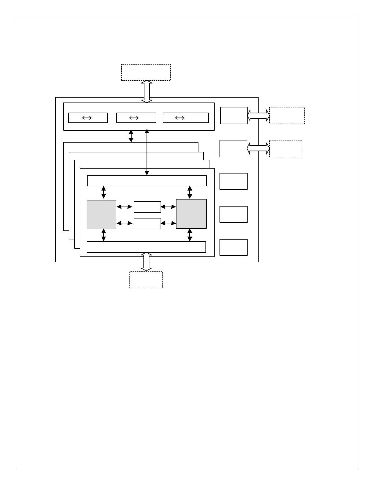
1.3 Block Diagram
RMII/SMII/
SS_SMII
PORT0
PORT1
...
PORT7
100M
Module
MAC Interface
MII RMII MII SS_S MIIMII SMII
MI I
Auto
Negotiation
Cable Broken
Detec tor
Driver
Twisted
Pair
Interface
10M
Module
LED
Display
SMI
Power
Management
CLOCK
GE NERAT OR
Voltage
Regulator
Serial /
Parallel
LED
MDC/MDIO
Figure 1-1 ADM7008 Block Diagram
1.4 Abbreviations
ANSI American National Standards Institute
BER Bit Error Rate
COL Collision
CRS Carrier Sense
CRSDV Carrier Sense and Data Valid
CTL Crystal
DSP Digital Signal Processor
DUPCOL Duplex and Collision
ESD End of Stream Delimiter
FEFI Far End Fault Indication
ADMtek Inc. 1-3
Page 11

ADM7008 Product Review
FIFO First In First Out
FLP Fast Link Pulse
FX Fiber
IA Information Application
LFSR Linear Feedback Shifter Register
LLP Low-power Link Pulse
LNKACT Link and Activity
LVTTL TTL Level
MAC Media Access Controller
MD Medium Detect
MDC Management Data Clock
MDIO Management Data Input/Output
MII Media Independent Interface
NRZ None Return to Zero
NRZI None Return to Zero Inverter
OP Operation Code
PCS Physical Coding Sub-layer
PECL Pseudo Emitter Couple Logic
PHY Physical Layer
PHYADDR PHY Address
PMA Physical Medium Attachment
PMD Physical Medium Dependent
PNP A type of Transistor
PQFP Plastic Quad Flat Pack
REFCLK Reference Clock
RF Remote Fault
RMII Reduced Media Independent Interface
RSMODE RMII/SMII/SS_SMII Mode Select
RXC Receive Clock
RXD Receive Data
RXDV Receive Data Valid
RXER Receive Data Error
RXN Receive Negative (Analog receive differential signal)
RXP Receive Positive (Analog receive differential signal)
RX_SYNC Receive Synchronous
SDN Signal Detect Negative (Fiber signal detect)
SDP Signal Detect Positive (Fiber signal detect)
SELFX Select Fiber
SMI Serial Management Interface
SMII Serial Media Independent Interface
SOHO Small Office and Home Office
SQE Signal Quality Error
SSD Start of Stream Delimiter
SS_SMII Source Synchronous Media Independent Interface
SYNC Synchronous
TA Turn Around
ADMtek Inc. 1-4
Page 12

ADM7008 Product Review
TDR Time Domain Reflectometry
TP Twisted Pair
TP-PMD Twisted Pair Physical Medium Dependent
TTL Transistor Transistor Logic
TXC Transmission Clock (MII)
TXCLK Transmission Clock (SMII/SS_SMII)
TXD Transmission Data
TXEN Transmission Enable
TXER Transmission Error
TXN Transmission Negative
TXP Transmission Positive
/J/K 5B signal to detect the start of a frame
/T/R 5B signal to detect the end of a frame
1.5 Conventions
1.5.1 Data Lengths
qword 64-bits
dword 32-bits
word 16-bits
byte 8 bits
nibble 4 bits
1.5.2 Register Type Descriptions
Register Type Description
RO Read Only
R/W Read and Write capable
SC Self-clearing
LL Latching low, unlatch on read
LH Latching high, unlatch on read
COR Clear On Read
1.5.3 Pin Type Descriptions
Pin Type Description
I: Input
O: Output
I/O: Bi-directional
OD: Open drain
SCHE: Schmitt Trigger
PU: Pull Up
PD: Pull Down
ADMtek Inc. 1-5
Page 13

ADM7008 Interface Description
Chapter 2 Interface Description
2.1 Pin Diagram
118
117
116
119
120
123
122
128
127
126
125
RXN0
VCCAD
RXP0
GNDRT
1
RXN1
2
RXP1
3
GND RT
4
TXN1
5
TXP1
6
VCCA2
7
TXP2
8
TXN2
9
GND RT
10
RXP2
11
RXN2
12
VCCAD
13
RXN3
14
RXP3
15
GND RT
16
TXN3
17
TXP3
18
VCCA2
19
TXP4
20
TXN4
21
GND RT
22
RXP4
23
RXN4
24
VCCAD
25
RXN5
6
2
RXP5
27
GND RT
28
TXN5
29
TXP5
30
VCCA2
31
TXP6
32
TXN6
33
GND RT
34
RXP6
35
RXN6
36
VCCAD
37
RXN7
38
RXP7
TXN7
RSMODE1
VCCA2
TXP7
GNDRT
121
124
RTX
VCCPLL2
VCCA2
TXP0
TXN0
GNDRCV
Revision A1
PHYADDR1
REFCLK_SEL
VCC2I K
GNDIK
RST_N
115
VCCAD
XI
XO
CONTROL
QFP 128
(REC_10M_P7) RXD1_P7/SPEED_LED_P7
(EN_AUTOMDIX) RXD0_ P7/R XD_P 7
LED_ DATA
LED_ CLK
111
114
113
112
110
109
108
107
106
105
104
103
VCC3O
GNDO
RXD1_P0/SPDLED_P0 (REC_10M_P0)
RXD0 _P0 /RXD_P0 (TESTSEL0)
CRSDV_P0 (SELFX0)
TXD1_ P0 /LNKAC T_P0
TXD0_ P0/TXD_P0
TXEN_ P0 /NA
REFCLK
GNDIK
SCAN_ MODE
SCAN_ EN
102
MDC
101
MDIO
GND IK
GND O
VCC3O
GND IK
100
99
98
97
96
95
94
93
92
91
90
89
88
87
86
85
84
83
82
81
80
79
78
77
76
75
74
73
72
71
70
69
68
67
66
65
TXEN_ P1 /NA
TXD0 _P 1/TX D_P 1
TXD1_P1/LNKACT_P1
CRS DV_P1 /NA (SELFX1)
RXD0 _P1 /RXD_P1 (TESTSEL1)
RXD1_P1/SPDLED_P1 (REC_10M_P1)
RXD0 _P2 /RXD_P2 (PHYADDR0 )
ADM7008
(REC_10M_P6) RXD1_P6/SPEED_LED_P6
(FX_PAUS E) CRSDV_ P7
TXD1_P7/LNKACT_P7
TXD0_ P7/TXD_P7
TXEN_ P7 /NA
VCC3O
GNDO
RXD1_P2/SPDLED_P2 (REC_10M_P2)
CR SD V_ P3 /R X_ SYNC (TESTS EL2 )
RXD0 _P3 /RXD_P3 (ANENDIS)
RXD1_P3 /SPDLED_P3 (REC_10M_P3)
CRSDV_P4/RX_CLK (DLY2NS)
RXD0 _P4 /R XD_P4 (TPDUPLEX)
RXD1_P4 /SPDLED_P4 (REC_10M_P4)
(LEDMD0) RXD0 _ P6/R XD_P 6
(RSMODE0) CRSDV_P6/NA
TXD1_P6/LNKACT_P6
CRSDV_P5 /NA (TP_PAUSE)
RXD0_P5/RXD_P5 (PWSAVE_DIS)
RXD1_P5 /SPDLED_P5 (REC_10M_P5)
TXD0_ P6/TXD_P6
TXEN_ P6 /NA
TXEN_ P2 /NA
TXD0 _P 2/TX D_P 2
TXD1_P2/LNKACT_P2
CRS DV_P2 (FXDUPLEX)
VCC2I K
TXEN_P3/TX_SYNC
TXD0 _P 3/TX D_P 3
TXD1_P3/LNKACT_P3
TXEN_ P4 /TX_ CLK
TXD0 _P 4/TX D_P 4
TXD1_P4/LNKACT_P4
VCC2I K
TXEN_ P5 /NA
TXD0 _P 5/TX D_P 5
TXD1_P5/LNKACT_P5
46474849505152535455565758596061626364
45
44
43
424140
39
Figure 2-1 ADM7008 Pin Assignment
ADMtek Inc. 2-1
Page 14

ADM7008 Interface Description
2.2 Pin Description
Note:
For those pins, which have multiple functions, pin name is separated by slash (“/”).
If not specified, all signals are default to digital signals.
Please refer to section ‘1.5.3 Pin Type Descriptions’ for an explanation of pin
abbreviations.
2.2.1 Twisted Pair Interface, 32 pins
Pin # Pin Name Type Description
123, 5, 7, 17
19, 29, 31, 41
124, 4, 8, 16
20, 28, 32, 40
126, 2, 10, 14
22, 26, 34, 38
127, 1, 11, 23
23, 25, 35, 37
TXP[0:7] O,
Analog
TXN[0:7] O,
Analog
RXP[0:7] I, Analog Twisted Pair Receive Input Positive.
RXN[0:7] I, Analog Twisted Pair Receive Input Negative.
Twisted Pair Transmit Output Positive.
Twisted Pair Transmit Output Negative.
2.2.2 Ground and Power, 20 pins
Pin # Pin Name Type Description
125, 3, 9, 15,
21, 27, 33, 39
118, 128, 12,
24, 36
122, 6, 18, 30,
42
120 GNDRCV Analog
121 VCCPLL2 Analog
GNDRT Analog
Ground
VCCAD Analog
Power
VCCA2 Analog
Power
Ground
Power
Analog Ground Pad
Analog 3.3V Power
Analog 1.8V Power
Analog Ground used by Clock Generator module
Analog 1.8V Power used by Clock Generator module
2.2.3 Mode Setting
Pin # Pin Name Type Description
43 RSMODE1 I, PD RMII and SMII/SS_SMII mode select signal. Dedicated input
provided by ADM7008 to determine the interface:
0: SMII or SS_SMII interface (See CRSDV_P6 power on setting
for more detail)
1: RMII interface
2.2.4 Clock Input Select
Pin # Pin Name Type Description
48 REFCLK_SEL I, PD XI/XO and REFCLK clock select signal. Dedicated input
provided by ADM7008 to determine the clock source for
ADM7008.
0: ADM7008 will use XI/XO as clock source for internal clock
generator. In this mode, REFCLK (pin 112) will output 50M
clock in RMII mode (RSMODE1 is set to 1) and 125M clock
in either SMII or SS_SMII mode (RSMODE1 is set to 0) \
1: ADM7008 will use the input of REFCLK (pin 112) as the
ADMtek Inc. 2-2
Page 15

ADM7008 Interface Description
A
Pin # Pin Name Type Description
clock source for internal clock generator.
Note: that when RSMODE1 is set to 1 (RMII mode), the input
of REFCLK should be 50M; when RSMODE1 is set to 0
(SMII or SS_SMII mode) the clock input on REFCLK
should be 125M
2.2.5 Clock Input, 3 pins
Pin # Pin Name Type Pin Description
115 XI/OSCI I, CTL Crystal/Oscillator input.
REFCLK_SEL = 0: 25M Crystal/Oscillator Input.
REFCLK_SEL = 1: Leave unconnected
116 XO O, CTL Crystal output. When 25M Oscillator is used, this pin should be
left unconnected. See XI/OSCI description above.
111 REFCLK I/O,
16mA
LVTTL
Reference clock. Function on this pin is highly depended upon
the setting on REFCLK_SEL and RSMODE1:
REFCLK_SEL RSMODE1 REFCLK (Direction/Frequency)
0 0 Output/125 MHz
0 1 Output/50 MHz
1 0 Input/125 MHz with maximum 100ppm
1 1 Input/50 MHz with maximum 100ppm
2.2.6 RMII/SMII Interface, 48 pins
Pin # Pin Name Type Pin Description
51, 52 Power On
Setting
REC_10M_P7,
EN_AUTOMDIX
RMII Mode
RXD[1:0]_P7
SMII/SS_SMII
Mode
SPDLED_P7,
SMII_RXD_P7
I/O,
8mA,
PD/PU
REC_10M: Value on RXD1_P7 will be latched by ADM7008
during power on reset as Port 7 10M Re-command value.
0: Recommend Port 7 to operate in 100M Mode
1: Recommend Port 7 to operate in 10M Mode
ADM7008 during power on reset as Auto MDIX function control
signal.
0: Disable all ports’ Auto MDIX function.
1: Enable all ports’ Auto MDIX function.
Port 7 RMII Receive Data. RXD[1:0] are the port 7 output dibits synchronously to REFCLK. Upon assertion of CRSDV_P,
RXD0 and RXD1 remain at 00 until valid data is output from the
FIFO onto RXD. 01 on RXD1 and RXD0 indicates the start of
valid data. If a false carrier or a symbol error is detected, RXD1
and RXD0 are set to 10 for the duration of the activity. Note
that in 100Mb/s mode RXD can change once per REFCLK
cycle, whereas in 10Mb/s mode RXD must be held steady for
10 consecutive REFCLK cycles.
Port 7 SMII Receive Data. RXD0 for the designated port
outputs data or in-band management information
synchronously to SMII REFCLK (pin 70). In 100Mb/s mode,
RXD0 outputs a new 10-bit segment starting with SYNC. In
10Mb/s mode, RXD0 must repeat each 10 bits segment 10
times. RXD1 for the designated port is acted as Speed Status
LED for port 7.
uto MDIX Enable signal: Value on RXD0_P7 will be latched by
ADMtek Inc. 2-3
Page 16

ADM7008 Interface Description
Pin # Pin Name Type Pin Description
SS_SMII Mode
SPDLED_P7,
SSS_SMII_RXD
_P7
53 Power On
Setting
FX_PAUSE
RMII Mode
CRSDV_P7
SMII/SS_SMII
Mode N/A
54, 55 RMII Mode
TXD[1:0]_P7
SMII Mode
LNKACT_P7,
SMII_TXD_P7
SMII Mode
LNKACT_P7,
SSSMII_TXD_P7
56 RMII Mode
TXEN_P7
SMII/SS_SMII
LOW
I, LVTTL,
O, 8mA
PD
I, TTL,
PD
I, TTL Port 7 Transmit Enable. Transmit Enable for port 7 indicates
Port 7 SS_SMII Receive Data. RXD0 for the designated port
outputs data or in-band management information
synchronously to RXCLK (pin 75). In 100Mb/s mode, RXD0
outputs a new 10-bit segment starting with SYNC. In 10Mb/s
mode, RXD0 must repeat each 10 bits segment 10 times.
RXD1 for the designated port is acted as Speed Status LED for
port 7.
Fiber PAUSE Recommend Value. Value on this pin will be
latched by ADM7008 during power on reset as Fiber port (See
SELFX power on setting for more detail) pause capability
control signal.
0: Pause off for all fiber ports
1: Pause on for all fiber ports
Port 7 Carrier Sense/Receive Data Valid. CRSDV_P7 asserts
when the receive medium is non-idle. The assertion of
CRSDV_P7 is asynchronous to REFCLK. At the de-assertion
of carrier, CRSDV_P7 de-asserts synchronously to REFCLK
only on the first di-bit of RXD. If there is still data in the FIFO
not yet presented onto RXD, then on the second di-bit of RXD,
CRSDV_P7 is asserted synchronously to REFCLK. The
toggling of CRSDV_P7 on the first and second di-bit continues
until all the data in the FIFO is presented onto RXD.
CRSDV_P7 is asserted for the duration of carrier activity for a
false carrier event.
Not used in SMII/SS_SMII Mode
Port 7 RMII Transmit Data. Transmit data for port 7 input the
di-bits that re transmitted and are driven synchronously to
REFCLK.
Note: that in 100Mb/s mode, TXD can change once per
REFCLK cycle, whereas in 10Mb/s mode, TXD must be held
steady for 10 consecutive REFCLK cycles.
Link and Activity LED/Port 7 SMII Transmit Data. TXD0 for port
7 inputs the data that is transmitted and is driven synchronously
to SMII_REFCLK (pin 70). In 100Mb/s mode, TXD0 inputs a
new 10-bit segment starting with SYNC. In 10Mb/s mode,
TXD0 must repeat each 10-bit segment 10 times. TXD1_P7
acts as Port 7 Link/Activity LED in both SMII and SS_SMII
Mode. See LED Description for more detail.
Link and Activity LED/Port 7 SS_SMII Transmit Data. TXD0 for
port 7 inputs the data that is transmitted and is driven
synchronously to TXCLK (pin 70). In 100Mb/s mode, TXD0
inputs a new 10-bit segment starting with SYNC. In 10Mb/s
mode, TXD0 must repeat each 10-bit segment 10 times.
that the di-bit on TXD is valid and it is driven synchronously to
REFCLK.
TIED TO LOW. TXEN_P7 should be tied to low for normal
operation.
ADMtek Inc. 2-4
Page 17

ADM7008 Interface Description
Pin # Pin Name Type Pin Description
59, 60
61
Power On
Setting
REC_10M_P6,
DUALLED
RMII Mode
RXD[1:0]_P6
SMII Mode
SPDLED_P6,
SMII_RXD_P6
SS_SMII Mode
SPDLED_P6,
SSSMII_RXD_P
6
Power On
Setting
RSMODE0
RMII Mode
CRSDV_P6
PD,
PD,
8mA
8mA
8mA
LVTTL,
PD
8mA
REC_10M: Value on RXD1_P6 will be latched by ADM7008
I
during power on reset as Port 6 10M Re-command value.
0: Recommend Port 6 to operate in 100M Mode
1: Recommend Port 6 to operate in 10M Mode
Dual Color LED Mode. Value on RXD0_P6 will be latched by
ADM7008 during power on reset to form LED control signal.
Value on this pin will affect the output value on Serial LED
output.
0: Single Color 3 bits/port serial stream (Default Value)
1: Dual Color 3 bits/port serial stream
Port 6 RMII Receive Data. RXD[1:0] are the port 6 output di-
O,
bits synchronously to REFCLK. Upon assertion of CRSDV_P,
RXD0 and RXD1 remain at 00 until valid data is output from the
FIFO onto RXD. The start of valid data is indicated by 01 on
RXD1 and RXD0. If a false carrier or a symbol error is
detected, RXD1 and RXD0 are set to 10 for the duration of the
activity. Note that in 100Mb/s mode RXD can change once per
REFCLK cycle, whereas in 10Mb/s mode RXD must be held
steady for 10 consecutive REFCLK cycles.
Port 6 SMII Receive Data. RXD0 for the designated port
O,
outputs data or in-band management information
synchronously to SMII REFCLK (pin 70). In 100Mb/s mode,
RXD0 outputs a new 10-bit segment starting with SYNC. In
10Mb/s mode, RXD0 must repeat each 10 bits segment 10
times. RXD1 for the designated port is acted as Speed Status
LED for port 6.
Port 6 SS_SMII Receive Data. RXD0 for the designated port
O,
outputs data or in-band management information
synchronously to RXCLK (pin 75). In 100Mb/s mode, RXD0
outputs a new 10-bit segment starting with SYNC. In 10Mb/s
mode, RXD0 must repeat each 10 bits segment 10 times.
RXD1 for the designated port is acted as Speed Status LED for
port 6.
RMII/SMII/SS_SMII Configuration bit 0. Value on this pin will
I,
be latched by ADM7008 during power on reset as interface
configuration bit 0. Combined with RSMODE1 (pin 43), three
possible interfaces are provided by ADM7008
RSMODE[1:0] Interface
00 SMII
01 SS_SMII
1x RMII
Port 6 Carrier Sense/Receive Data Valid. CRSDV_P6 asserts
O,
when the receive medium is non-idle. The assertion of
CRSDV_P6 is asynchronous to REFCLK. At the de-assertion
of carrier, CRSDV_P6 de-asserts synchronously to REFCLK
only on the first di-bit of RXD. If there is still data in the FIFO
not yet presented onto RXD, then on the second di-bit of RXD,
ADMtek Inc. 2-5
Page 18

ADM7008 Interface Description
g
Pin # Pin Name Type Pin Description
62, 63
64
65, 66
SMII/SS_SMII
Mode
N/A
RMII Mode
TXD[1:0]_P6
SMII Mode
LNKACT_P6,
SMII_TXD_P6
SS_SMII Mode
LNKACT_P6,
SSSMII_TXD_P6
RMII Mode
TXEN_P6
SMII/SS_SMII
LOW
Power On
Setting
REC_10M_P5,
PWSAVE_DIS
RMII Mode
RXD[1:0]_P5
LVTTL,
PD,
PD
TTL
I,
PD,
PD
O,
8mA
CRSDV_P6 is asserted synchronously to REFCLK. The
toggling of CRSDV_P6 on the first and second di-bit continues
until all the data in the FIFO is presented onto RXD.
CRSDV_P6 is asserted for the duration of carrier activity for a
false carrier event.
Not Used.
Not used in SMII/SS_SMII Mode
I,
Port 6 RMII Transmit Data. Transmit data for port 6 input the
di-bits that re transmitted and are driven synchronously to
REFCLK. Note that in 100Mb/s mode, TXD can change once
per REFCLK cycle, whereas in 10Mb/s mode, TXD must be
held steady for 10 consecutive REFCLK cycles.
Link and Activity LED/Port 6 SMII Transmit Data. TXD0 for port
6 inputs the data that is transmitted and is driven synchronously
to SMII_REFCLK (pin 70). In 100Mb/s mode, TXD0 inputs a
new 10-bit segment starting with SYNC. In 10Mb/s mode,
TXD0 must repeat each 10-bit segment 10 times.
TXD1_P6 acts as Port 6 Link/Activity LED in both SMII and
SS_SMII Mode. See LED Description for more detail.
Link and Activity LED/Port 6 SS_SMII Transmit Data. TXD0 for
port 6 inputs the data that is transmitted and is driven
synchronously to TXCLK (pin 70). In 100Mb/s mode, TXD0
inputs a new 10-bit segment starting with SYNC. In 10Mb/s
mode, TXD0 must repeat each 10-bit segment 10 times.
I,
Port 6 Transmit Enable. Transmit Enable for port 6 indicates
that the di-bit on TXD is valid and it is driven synchronously to
REFCLK.
TIED TO LOW. TXEN_P6 should be tied to low for normal
operation in both SMII and SS_SMII Mode.
REC_10M: Value on RXD1_P5 will be latched by ADM7008
during power on reset as Port 5 10M Re-command value.
0: Recommend Port 5 to operate in 100M Mode (Default)
1: Recommend Port 5 to operate in 10M Mode
Lower power Link Pulse Function (Power Saving, LLP) Disable.
Value on RXD1 will be latched by ADM7008 during power on
reset as power saving disable signal. (See Lower Power Link
Pulse Function description for more detail)
0: Power Saving Enable
1: Power Saving disable (Default)
Port 5 RMII Receive Data. RXD[1:0] are the port 5 output dibits synchronously to REFCLK. Upon assertion of CRSDV_P,
RXD0 and RXD1 remain at 00 until valid data is output from the
FIFO onto RXD. 01 on RXD1 and RXD0 indicates the start of
valid data. If a false carrier or a symbol error is detected, RXD1
and RXD0 are set to 10 for the duration of the activity. Note
that in 100Mb/s mode RXD can chan
e once per REFCLK
ADMtek Inc. 2-6
Page 19

ADM7008 Interface Description
Pin # Pin Name Type Pin Description
67
68, 69
SMII Mode
SPDLED_P5,
SMII_RXD_P5
SS_SMII Mode
SPDLED_P5,
SSSMII_RXD_P
5
Power On
Setting
TP_PAUSE
RMII Mode
CRSDV_P5
SMII/SS_SMII
Mode
N/A
RMII Mode
TXD[1:0]_P5
SMII Mode
LNKACT_P5,
SMII_TXD_P5
LVTTL,
PU
8mA
TTL,
PD
cycle, whereas in 10Mb/s mode RXD must be held steady for
10 consecutive REFCLK cycles.
Port 5 SMII Receive Data. RXD0 for the designated port
outputs data or in-band management information
synchronously to SMII REFCLK (pin 70). In 100Mb/s mode,
RXD0 outputs a new 10-bit segment starting with SYNC. In
10Mb/s mode, RXD0 must repeat each 10 bits segment 10
times. RXD1 for the designated port is acted as Speed Status
LED for port 5.
Port 5 SS_SMII Receive Data. RXD0 for the designated port
outputs data or in-band management information
synchronously to RXCLK (pin 75). In 100Mb/s mode, RXD0
outputs a new 10-bit segment starting with SYNC. In 10Mb/s
mode, RXD0 must repeat each 10 bits segment 10 times.
RXD1 for the designated port is acted as Speed Status LED for
port 5.
I,
Twisted Pair PAUSE Recommend Value. Value on this pin will
be latched by ADM7008 during power on reset as twisted pair
port (See SELFX power on setting for more detail) pause
capability control signal.
0: Pause off for all twisted pair ports
1: Pause on for all twisted pair ports
O,
Port 5 Carrier Sense/Receive Data Valid. CRSDV_P5 asserts
when the receive medium is non-idle. The assertion of
CRSDV_P5 is asynchronous to REFCLK. At the de-assertion
of carrier, CRSDV_P5 de-asserts synchronously to REFCLK
only on the first di-bit of RXD. If there is still data in the FIFO
not yet presented onto RXD, then on the second di-bit of RXD,
CRSDV_P5 is asserted synchronously to REFCLK. The
toggling of CRSDV_P5 on the first and second di-bit continues
until all the data in the FIFO is presented onto RXD.
CRSDV_P5 is asserted for the duration of carrier activity for a
false carrier event.
Not Used.
Not used in SMII/SS_SMII Mode
I,
Port 5 RMII Transmit Data. Transmit data for port 5 inputs the
di-bits that re transmitted and are driven synchronously to
REFCLK. Note that in 100Mb/s mode, TXD can change once
per REFCLK cycle, whereas in 10Mb/s mode, TXD must be
held steady for 10 consecutive REFCLK cycles.
Link and Activity LED/Port 5 SMII Transmit Data. TXD0 for port
5 inputs the data that is transmitted and is driven synchronously
to SMII_REFCLK (pin 70). In 100Mb/s mode, TXD0 inputs a
new 10-bit segment starting with SYNC. In 10Mb/s mode,
TXD0 must repeat each 10-bit segment 10 times.
TXD1_P5 acts as Port 5 Link/Activity LED in both SMII and
SS_SMII Mode. See LED Description for more detail.
ADMtek Inc. 2-7
Page 20

ADM7008 Interface Description
Pin # Pin Name Type Pin Description
70
73, 74
75
SS_SMII Mode
LNKACT_P5,
SSSMII_TXD_P5
RMII Mode
TXEN_P5
SMII/SS_SMII
LOW
Power On
Setting
REC_10M_P4,
TP_DUPLEX
RMII Mode
RXD[1:0]_P4
SMII Mode
SPDLED_P4,
SMII_RXD_P4
SS_SMII Mode
SPDLED_P4,
SSSMII_RXD_P
4
Power On
Setting
DLY2NS
TTL
I/O,
8mA,
PD/PU
LVTTL,
PD
Link and Activity LED/Port 5 SS_SMII Transmit Data. TXD0 for
port 5 inputs the data that is transmitted and is driven
synchronously to TXCLK (pin 70). In 100Mb/s mode, TXD0
inputs a new 10-bit segment starting with SYNC. In 10Mb/s
mode, TXD0 must repeat each 10-bit segment 10 times.
I,
Port 5 Transmit Enable. Transmit Enable for port 5 indicates
that the di-bit on TXD is valid and it is driven synchronously to
REFCLK.
SMII/SS_SMII Mode. Keep LOW for normal operation.
REC_10M: Value on RXD1_P4 will be latched by ADM7008
during power on reset as Port 4 10M Re-command value.
0: Recommend Port 4 to operate in 100M Mode
1: Recommend Port 4 to operate in 10M Mode
Twisted Pair Duplex Recommend Value. Value on RXD1 will
be latched by ADM7008 during power on reset as duplex
recommend value for twisted pair interface.
0: Half Duplex for all twisted pair ports
1: Full Duplex for all twisted pair ports
Port 4 RMII Receive Data. RXD[1:0] are the port 4 output dibits synchronously to REFCLK. Upon assertion of CRSDV_P,
RXD0 and RXD1 remain at 00 until valid data is output from the
FIFO onto RXD. 01 on RXD1 and RXD0 indicates the start of
valid data. If a false carrier or a symbol error is detected, RXD1
and RXD0 are set to 10 for the duration of the activity. Note
that in 100Mb/s mode RXD can change once per REFCLK
cycle, whereas in 10Mb/s mode RXD must be held steady for
10 consecutive REFCLK cycles.
Port 4 SMII Receive Data. RXD0 for the designated port
outputs data or in-band management information
synchronously to SMII REFCLK (pin 70). In 100Mb/s mode,
RXD0 outputs a new 10-bit segment starting with SYNC. In
10Mb/s mode, RXD0 must repeat each 10 bits segment 10
times. RXD1 for the designated port is acted as Speed Status
LED for port 4.
Port 4 SS_SMII Receive Data. RXD0 for the designated port
outputs data or in-band management information
synchronously to RXCLK (pin 75). In 100Mb/s mode, RXD0
outputs a new 10-bit segment starting with SYNC. In 10Mb/s
mode, RXD0 must repeat each 10 bits segment 10 times.
RXD1 for the designated port is acted as Speed Status LED for
port 4.
I,
REFCLK Delay 2ns. Value on this pin will be latched by
ADM7008 during power on reset as delay select signal for
REFCLK input when REFCLK_SEL and RSMODE1 are both
set to 1 (RMII interface with REFCLK as clock input)
ADMtek Inc. 2-8
Page 21

ADM7008 Interface Description
/
Pin # Pin Name Type Pin Description
76, 77
78
RMII Mode
CRSDV_P4
SMII Mode
N/A
SS_SMII Mode
RXCLK
RMII Mode
TXD[1:0]_P4
SMII Mode
LNKACT_P4,
SMII_TXD_P4
SS_SMII Mode
LNKACT_P4,
SSSMII_TXD_P4
RMII Mode
TXEN_P4
SMII Mode
SMII_REFCLK
O,
8mA
I,
TTL,
PD
I,
TTL
0: Normal REFCLK clock path
1: REFCLK delay by 2 ns
Port 4 Carrier Sense/Receive Data Valid. CRSDV_P4 asserts
when the receive medium is non-idle. The assertion of
CRSDV_P4 is asynchronous to REFCLK. At the de-assertion
of carrier, CRSDV_P4 de-asserts synchronously to REFCLK
only on the first di-bit of RXD. If there is still data in the FIFO
not yet presented onto RXD, then on the second di-bit of RXD,
CRSDV_P4 is asserted synchronously to REFCLK. The
toggling of CRSDV_P4 on the first and second di-bit continues
until all the data in the FIFO is presented onto RXD.
CRSDV_P4 is asserted for the duration of carrier activity for a
false carrier event.
Not Used.
Not used in SMII Mode
125M Receive Clock. This pin acts as 125M receive clock
when ADM7008 is programmed to SS_SMII mode. All
SSS_SMII_RXD are synchronous to the rising edge of this
clock.
Note: that clock on this pin will not be active during power on
reset due to power on setting.
Port 4 RMII Transmit Data. Transmit data for port 4 inputs the
di-bits that re transmitted and are driven synchronously to
REFCLK. Note that in 100Mb/s mode, TXD can change once
per REFCLK cycle, whereas in 10Mb/s mode, TXD must be
held steady for 10 consecutive REFCLK cycles.
Link and Activity LED
4 inputs the data that is transmitted and is driven synchronously
to SMII_REFCLK (pin 70). In 100Mb/s mode, TXD0 inputs a
new 10-bit segment starting with SYNC. In 10Mb/s mode,
TXD0 must repeat each 10-bit segment 10 times.
TXD1_P4 acts as Port 4 Link/Activity LED in both SMII and
SS_SMII Mode. See LED Description for more detail.
Link and Activity LED/Port 4 SS_SMII Transmit Data. TXD0 for
port 4 inputs the data that is transmitted and is driven
synchronously to TXCLK (pin 70). In 100Mb/s mode, TXD0
inputs a new 10-bit segment starting with SYNC. In 10Mb/s
mode, TXD0 must repeat each 10-bit segment 10 times.
Port 4 Transmit Enable. Transmit Enable for port 4 indicates
that the di-bit on TXD is valid and it is driven synchronously to
REFCLK.
SMII 125M Reference Clock. In SMII Mode, this pin acts as
125M reference clock for all ports. All transmit and receive data
(include transmit enable and receive data valid) should be
synchronous to the rising edge of this clock.
Port 4 SMII Transmit Data. TXD0 for port
ADMtek Inc. 2-9
Page 22

ADM7008 Interface Description
Pin # Pin Name Type Pin Description
81, 82
83
SS_SMII Mode
TXCLK
Power On
Setting
REC_10M_P3,
ANENDIS
RMII Mode
RXD[1:0]_P3
SMII Mode
SPDLED_P3,
SMII_RXD_P3
SS_SMII Mode
SPDLED_P3,
SSSMII_RXD_P
3
Power On
Setting
TESTSEL2
RMII Mode
CRSDV_P3
I/O,
8mA,
PD
PD
8mA
SS_SMII 125M Transmit Clock. In SS_SMII Mode, this pin acts
as 125M transmit clock for all ports. TXD and TXEN should be
synchronous to the rising edge of this clock.
REC_10M: Value on RXD1_P3 will be latched by ADM7008
during power on reset as Port 3 10M Re-command value.
0: Recommend Port 3 to operate in 100M Mode
1: Recommend Port 3 to operate in 10M Mode
Twisted Pair Duplex Recommend Value. Value on RXD1 will
be latched by ADM7008 during power on reset as auto
negotiation disable recommend value for twisted pair interface.
0: Auto-negotiation Enable for all twisted pair ports.
1: Auto-negotiation Disable for all twisted pair ports
Port 3 RMII Receive Data. RXD[1:0] are the port 3 output dibits synchronously to REFCLK. Upon assertion of CRSDV_P,
RXD0 and RXD1 remain at 00 until valid data is output from the
FIFO onto RXD. The start of valid data is indicated by 01 on
RXD1 and RXD0. If a false carrier or a symbol error is
detected, RXD1 and RXD0 are set to 10 for the duration of the
activity. Note that in 100Mb/s mode RXD can change once per
REFCLK cycle, whereas in 10Mb/s mode RXD must be held
steady for 10 consecutive REFCLK cycles.
Port 3 SMII Receive Data. RXD0 for the designated port
outputs data or in-band management information
synchronously to SMII REFCLK (pin 70). In 100Mb/s mode,
RXD0 outputs a new 10-bit segment starting with SYNC. In
10Mb/s mode, RXD0 must repeat each 10 bits segment 10
times. RXD1 for the designated port is acted as Speed Status
LED for port 3.
Port 3 SS_SMII Receive Data. RXD0 for the designated port
outputs data or in-band management information
synchronously to RXCLK (pin 75). In 100Mb/s mode, RXD0
outputs a new 10-bit segment starting with SYNC. In 10Mb/s
mode, RXD0 must repeat each 10 bits segment 10 times.
RXD1 for the designated port is acted as Speed Status LED for
port 3.
I,
Industrial Test Mode Select 2. Value on this pin will be latched
by ADM7008 during power on reset as industrial test mode
select bit 2. Pull down for normal operation. For Test Mode,
See test select 0 for more detail
O,
Port 3 Carrier Sense/Receive Data Valid. CRSDV_P3 asserts
when the receive medium is non-idle. The assertion of
CRSDV_P3 is asynchronous to REFCLK. At the de-assertion
of carrier, CRSDV_P3 de-asserts synchronously to REFCLK
only on the first di-bit of RXD. If there is still data in the FIFO
not yet presented onto RXD, then on the second di-bit of RXD,
CRSDV_P3 is asserted synchronously to REFCLK. The
toggling of CRSDV_P3 on the first and second di-bit continues
ADMtek Inc. 2-10
Page 23

ADM7008 Interface Description
Pin # Pin Name Type Pin Description
84, 85
86
89, 90
SMII Mode
N/A
SS_SMII Mode
RX_SYNC
RMII Mode
TXD[1:0]_P3
SMII Mode
LNKACT_P3,
SMII_TXD_P3
SS_SMII Mode
LNKACT_P3,
SSSMII_TXD_P3
RMII Mode
TXEN_P3
SMII Mode
SMII_SYNC
SS_SMII Mode
TX_SYNC
Power On
Setting
REC_10M_P2,
PHYADDR0
RMII Mode
RXD[1:0]_P2
TTL,
PD
TTL
PD,
PD
8mA
until all the data in the FIFO is presented onto RXD.
CRSDV_P3 is asserted for the duration of carrier activity for a
false carrier event.
Not Used.
Not used in SMII Mode
SS_SMII Receive Synchronization Signal. In SS_SMII Mode,
this pin sets the bit stream alignment of SSS_SMII_RXD for all
ports.
I,
Port 3 RMII Transmit Data. Transmit data for port 3 inputs the
di-bits that re transmitted and are driven synchronously to
REFCLK. Note that in 100Mb/s mode, TXD can change once
per REFCLK cycle, whereas in 10Mb/s mode, TXD must be
held steady for 10 consecutive REFCLK cycles.
Link and Activity LED/Port 3 SMII Transmit Data. TXD0 for port
3 inputs the data that is transmitted and is driven synchronously
to SMII_REFCLK (pin 70). In 100Mb/s mode, TXD0 inputs a
new 10-bit segment starting with SYNC. In 10Mb/s mode,
TXD0 must repeat each 10-bit segment 10 times.
TXD1_P3 acts as Port 3 Link/Activity LED in both SMII and
SS_SMII Mode. See LED Description for more detail.
Link and Activity LED/Port 3 SS_SMII Transmit Data. TXD0 for
port 3 inputs the data that is transmitted and is driven
synchronously to TXCLK (pin 70). In 100Mb/s mode, TXD0
inputs a new 10-bit segment starting with SYNC. In 10Mb/s
mode, TXD0 must repeat each 10-bit segment 10 times.
I,
Port 3 Transmit Enable. Transmit Enable for port 3 indicates
that the di-bit on TXD is valid and it is driven synchronously to
REFCLK.
SMII Synchronization Signal. In SMII Mode, this pin sets the bit
stream alignment of SMII_TXD and SMII_RXD for all ports.
SS_SMII Transmit Synchronization Signal. In SS_SMII Mode,
this pin sets the bit stream alignment of SSS_SMII_TXD for all
ports.
REC_10M: Value on RXD1_P2 will be latched by ADM7008
I,
during power on reset as Port 2 10M Re-command value.
0: Recommend Port 2 to operate in 100M Mode (100M)
1: Recommend Port 2 to operate in 10M Mode
PHY Address Bit 0. Value on RXD1 will be latched by
ADM7008 during power on reset as PHY address bit 0.
Combined with PHYADDR1 (pin 44) to form PHY address for
ADM7008. See PHYADDR1 description for more detail
Port 2 RMII Receive Data. RXD[1:0] are the port 2 output di-
O,
bits synchronously to REFCLK. Upon assertion of CRSDV_P,
RXD0 and RXD1 remain at 00 until valid data is output from the
ADMtek Inc. 2-11
Page 24

ADM7008 Interface Description
Pin # Pin Name Type Pin Description
91
92, 93
SMII Mode
SPDLED_P2,
SMII_RXD_P2
SS_SMII Mode
SPDLED_P2,
SSSMII_RXD_P
2
Power On
Setting
FX_DUPLEX
RMII Mode
CRSDV_P2
SMII/SS_SMII
Mode
N/A
RMII Mode
TXD[1:0]_P2
SMII Mode
LNKACT_P2,
SMII_TXD_P2
I/O,
8mA
PU
TTL,
PD
FIFO onto RXD. The start of valid data is indicated by 01 on
RXD1 and RXD0. If a false carrier or a symbol error is
detected, RXD1 and RXD0 are set to 10 for the duration of the
activity. Note that in 100Mb/s mode RXD can change once per
REFCLK cycle, whereas in 10Mb/s mode RXD must be held
steady for 10 consecutive REFCLK cycles.
Port 2 SMII Receive Data. RXD0 for the designated port
outputs data or in-band management information
synchronously to SMII REFCLK (pin 70). In 100Mb/s mode,
RXD0 outputs a new 10-bit segment starting with SYNC. In
10Mb/s mode, RXD0 must repeat each 10 bits segment 10
times. RXD1 for the designated port is acted as Speed Status
LED for port 2.
Port 2 SS_SMII Receive Data. RXD0 for the designated port
outputs data or in-band management information
synchronously to RXCLK (pin 75). In 100Mb/s mode, RXD0
outputs a new 10-bit segment starting with SYNC. In 10Mb/s
mode, RXD0 must repeat each 10 bits segment 10 times.
RXD1 for the designated port is acted as Speed Status LED for
port 2.
Duplex Recommend Value for Fiber Port. Value on this pin will
be latched by ADM7008 during power on reset as duplex
recommend value for all fiber ports.
0: Half duplex for all fiber ports.
1: Full duplex for all fiber ports.
Port 2 Carrier Sense/Receive Data Valid. CRSDV_P2 asserts
when the receive medium is non-idle. The assertion of
CRSDV_P2 is asynchronous to REFCLK. At the de-assertion
of carrier, CRSDV_P2 de-asserts synchronously to REFCLK
only on the first di-bit of RXD. If there is still data in the FIFO
not yet presented onto RXD, then on the second di-bit of RXD,
CRSDV_P2 is asserted synchronously to REFCLK. The
toggling of CRSDV_P2 on the first and second di-bit continues
until all the data in the FIFO is presented onto RXD.
CRSDV_P2 is asserted for the duration of carrier activity for a
false carrier event.
Not Used.
Not used in SMII and SS_SMII Mode
I,
Port 2 RMII Transmit Data. Transmit data for port 2 inputs the
di-bits that re transmitted and are driven synchronously to
REFCLK. Note that in 100Mb/s mode, TXD can change once
per REFCLK cycle, whereas in 10Mb/s mode, TXD must be
held steady for 10 consecutive REFCLK cycles.
Link and Activity LED/Port 2 SMII Transmit Data. TXD0 for port
2 inputs the data that is transmitted and is driven synchronously
to SMII_REFCLK (pin 70). In 100Mb/s mode, TXD0 inputs a
ADMtek Inc. 2-12
Page 25

ADM7008 Interface Description
Pin # Pin Name Type Pin Description
94
95, 96
97
SS_SMII Mode
LNKACT_P2,
SSSMII_TXD_P2
RMII Mode
TXEN_P2
SMII/SS_SMII
LOW
Power On
Setting
REC_10M_P1,
TESTSEL1
RMII Mode
RXD[1:0]_P1
SMII Mode
SPDLED_P1,
SMII_RXD_P1
SS_SMII Mode
SPDLED_P1,
SSSMII_RXD_P
1
Power On
TTL
I/O,
8mA,
PD
I/O, Fiber/Twisted Pair Configuration bit 1. Value on RXD1 will be
new 10-bit segment starting with SYNC. In 10Mb/s mode,
TXD0 must repeat each 10-bit segment 10 times.
TXD1_P2 acts as Port 2 Link/Activity LED in both SMII and
SS_SMII Mode. See LED Description for more detail.
Link and Activity LED/Port 2 SS_SMII Transmit Data. TXD0 for
port 2 inputs the data that is transmitted and is driven
synchronously to TXCLK (pin 70). In 100Mb/s mode, TXD0
inputs a new 10-bit segment starting with SYNC. In 10Mb/s
mode, TXD0 must repeat each 10-bit segment 10 times.
I,
Port 2 Transmit Enable. Transmit Enable for port 2 indicates
that the di-bit on TXD is valid and it is driven synchronously to
REFCLK.
Not Used. Tied to LOW for normal operation in SMII/SS_SMII
mode.
REC_10M: Value on RXD1_P1 will be latched by ADM7008
during power on reset as Port 1 10M Re-command value.
0: Recommend Port 1 to operate in 100M Mode
1: Recommend Port 1 to operate in 10M Mode
Industrial Test Mode Select 1. Value on RXD0_P1 will be
latched by ADM7008 during power on reset as industrial test
mode select bit 1. Pull down for normal operation. For Test
Mode, See test select 0 for more detail
Port 1 RMII Receive Data. RXD[1:0] are the port 1 output dibits synchronously to REFCLK. Upon assertion of CRSDV_P,
RXD0 and RXD1 remain at 00 until valid data is output from the
FIFO onto RXD. The start of valid data is indicated by 01 on
RXD1 and RXD0. If a false carrier or a symbol error is
detected, RXD1 and RXD0 are set to 10 for the duration of the
activity. Note that in 100Mb/s mode RXD can change once per
REFCLK cycle, whereas in 10Mb/s mode RXD must be held
steady for 10 consecutive REFCLK cycles.
Port 1 SMII Receive Data. RXD0 for the designated port
outputs data or in-band management information
synchronously to SMII REFCLK (pin 70). In 100Mb/s mode,
RXD0 outputs a new 10-bit segment starting with SYNC. In
10Mb/s mode, RXD0 must repeat each 10 bits segment 10
times. RXD1 for the designated port is acted as Speed Status
LED for port 1.
Port 1 SS_SMII Receive Data. RXD0 for the designated port
outputs data or in-band management information
synchronously to RXCLK (pin 75). In 100Mb/s mode, RXD0
outputs a new 10-bit segment starting with SYNC. In 10Mb/s
mode, RXD0 must repeat each 10 bits segment 10 times.
RXD1 for the designated port is acted as Speed Status LED for
port 1.
ADMtek Inc. 2-13
Page 26

ADM7008 Interface Description
Pin # Pin Name Type Pin Description
98, 99
100
Setting
SELFX1
RMII Mode
CRSDV_P1
SMII/SS_SMII
Mode
N/A
RMII Mode
TXD[1:0]_P1
SMII Mode
LNKACT_P1,
SMII_TXD_P1
SS_SMII Mode
LNKACT_P1,
SSSMII_TXD_P1
RMII Mode
TXEN_P1
SMII/SS_SMII
LOW
8mA
PD
I,
TTL,
PD
I,
TTL
latched by ADM7008 during power on reset as fiber/twisted pair
interface configuration bit 1. Combined with SELFX0 (Power
On setting value on RXD0_P0) to program ADM7008 into 4
different modes.
00: all ports are twisted ports
01: only port 7 is fiber port, and all the other ports are twisted
ports.
10: only port 7 and port 6 are fiber ports, and all the other port
are twisted
port
11: all ports are fiber ports.
Port 1 Carrier Sense/Receive Data Valid. CRSDV_P1 asserts
when the receive medium is non-idle. The assertion of
CRSDV_P1 is asynchronous to REFCLK. At the de-assertion
of carrier, CRSDV_P1 de-asserts synchronously to REFCLK
only on the first di-bit of RXD. If there is still data in the FIFO
not yet presented onto RXD, then on the second di-bit of RXD,
CRSDV_P1 is asserted synchronously to REFCLK. The
toggling of CRSDV_P1 on the first and second di-bit continues
until all the data in the FIFO is presented onto RXD.
CRSDV_P1 is asserted for the duration of carrier activity for a
false carrier event.
Not Used.
Not used in SMII and SS_SMII Mode
Port 1 RMII Transmit Data. Transmit data for port 1 inputs the
di-bits that re transmitted and are driven synchronously to
REFCLK. Note that in 100Mb/s mode, TXD can change once
per REFCLK cycle, whereas in 10Mb/s mode, TXD must be
held steady for 10 consecutive REFCLK cycles.
Link and Activity LED/Port 1 SMII Transmit Data. TXD0 for port
1 inputs the data that is transmitted and is driven synchronously
to SMII_REFCLK (pin 70). In 100Mb/s mode, TXD0 inputs a
new 10-bit segment starting with SYNC. In 10Mb/s mode,
TXD0 must repeat each 10-bit segment 10 times.
TXD1_P1 acts as Port 1 Link/Activity LED in both SMII and
SS_SMII Mode. See LED Description for more detail.
Link and Activity LED/Port 1 SS_SMII Transmit Data. TXD0 for
port 1 inputs the data that is transmitted and is driven
synchronously to TXCLK (pin 70). In 100Mb/s mode, TXD0
inputs a new 10-bit segment starting with SYNC. In 10Mb/s
mode, TXD0 must repeat each 10-bit segment 10 times.
Port 1 Transmit Enable. Transmit Enable for port 1 indicates
that the di-bit on TXD is valid and it is driven synchronously to
REFCLK.
Not Used. Tied to LOW for normal operation in SMII/SS_SMII
mode.
ADMtek Inc. 2-14
Page 27

ADM7008 Interface Description
Pin # Pin Name Type Pin Description
105, 106
107
Power On
Setting
REC_10M_P0,
TESTSEL0
RMII Mode
RXD[1:0]_P0
SMII Mode
SPDLED_P0,
SMII_RXD_P0
SS_SMII Mode
SPDLED_P0,
SSSMII_RXD_P
0
Power On
Setting
SELFX0
RMII Mode
CRSDV_P0
I/O,
8mA,
PD
I/O,
8mA
PD
REC_10M: Value on RXD1_P0 will be latched by ADM7008
during power on reset as Port 0 10M Re-command value.
0: Recommend Port 0 to operate in 100M Mode
1: Recommend Port 0 to operate in 10M Mode
Industrial Test Mode Select 0. Value on RXD0_P1 will be
latched by ADM7008 during power on reset as industrial test
mode select bit 0. Pull down TESTSEL[2:0] for normal
operation.
TESTSEL Mode
000: Normal Mode
Port 0 RMII Receive Data. RXD[1:0] are the port 0 output dibits synchronously to REFCLK. Upon assertion of CRSDV_P,
RXD0 and RXD1 remain at 00 until valid data is output from the
FIFO onto RXD. The start of valid data is indicated by 01 on
RXD1 and RXD0. If a false carrier or a symbol error is
detected, RXD1 and RXD0 are set to 10 for the duration of the
activity. Note that in 100Mb/s mode RXD can change once per
REFCLK cycle, whereas in 10Mb/s mode RXD must be held
steady for 10 consecutive REFCLK cycles.
Port 0 SMII Receive Data. RXD0 for the designated port
outputs data or in-band management information
synchronously to SMII REFCLK (pin 70). In 100Mb/s mode,
RXD0 outputs a new 10-bit segment starting with SYNC. In
10Mb/s mode, RXD0 must repeat each 10 bits segment 10
times. RXD1 for the designated port is acted as Speed Status
LED for port 0.
Port 0 SS_SMII Receive Data. RXD0 for the designated port
outputs data or in-band management information
synchronously to RXCLK (pin 75). In 100Mb/s mode, RXD0
outputs a new 10-bit segment starting with SYNC. In 10Mb/s
mode, RXD0 must repeat each 10 bits segment 10 times.
RXD1 for the designated port is acted as Speed Status LED for
port 0.
Fiber/Twisted Pair Configuration bit 0. Value on RXD1 will be
latched by ADM7008 during power on reset as fiber/twisted pair
interface configuration bit 1. Combined with SELFX1 (Power
On setting value on RXD0_P1) to program ADM7008 into 4
different modes. See SELFX1 for more detail
Port 0 Carrier Sense/Receive Data Valid. CRSDV_P0 asserts
when the receive medium is non-idle. The assertion of
CRSDV_P0 is asynchronous to REFCLK. At the de-assertion
of carrier, CRSDV_P0 de-asserts synchronously to REFCLK
only on the first di-bit of RXD. If there is still data in the FIFO
not yet presented onto RXD, then on the second di-bit of RXD,
CRSDV_P0 is asserted synchronously to REFCLK. The
toggling of CRSDV_P0 on the first and second di-bit continues
until all the data in the FIFO is presented onto RXD.
ADMtek Inc. 2-15
Page 28

ADM7008 Interface Description
p
Pin # Pin Name Type Pin Description
108, 109
110
SMII/SS_SMII
Mode
N/A
RMII Mode
TXD[1:0]_P0
SMII Mode
LNKACT_P0,
SMII_TXD_P0
SS_SMII Mode
LNKACT_P0,
SSSMII_TXD_P0
RMII Mode
TXEN_P0
SMII/SS_SMII
LOW
TTL,
PD
TTL
CRSDV_P0 is asserted for the duration of carrier activity for a
false carrier event.
Not Used.
Not used in SMII and SS_SMII Mode
I,
Port 0 RMII Transmit Data. Transmit data for port 1 inputs the
di-bits that re transmitted and are driven synchronously to
REFCLK. Note that in 100Mb/s mode, TXD can change once
per REFCLK cycle, whereas in 10Mb/s mode, TXD must be
held steady for 10 consecutive REFCLK cycles.
Link and Activity LED/Port 0 SMII Transmit Data. TXD0 for port
0 inputs the data that is transmitted and is driven synchronously
to SMII_REFCLK (pin 70). In 100Mb/s mode, TXD0 inputs a
new 10-bit segment starting with SYNC. In 10Mb/s mode,
TXD0 must repeat each 10-bit segment 10 times.
TXD1_P0 acts as Port 0 Link/Activity LED in both SMII and
SS_SMII Mode. See LED Description for more detail.
Link and Activity LED/Port 0 SS_SMII Transmit Data. TXD0 for
port 1 inputs the data that is transmitted and is driven
synchronously to TXCLK (pin 70). In 100Mb/s mode, TXD0
inputs a new 10-bit segment starting with SYNC. In 10Mb/s
mode, TXD0 must repeat each 10-bit segment 10 times.
I,
Port 0 Transmit Enable. Transmit Enable for port 0 indicates
that the di-bit on TXD is valid and it is driven synchronously to
REFCLK.
Not Used. Tied to LOW for normal operation in SMII/SS_SMII
mode.
2.2.7 ATPG Signals, 2 pins
Pin # Pin Name Type Description
114 SCAN_EN I
VLTTL
113 SCAN_MODE I
VLTTL
SCAN_EN: Scan enable for test 0: Normal mode
SCAN_MODE: Scan mode select for test 0: Normal mode
2.2.8 Reset Pin
Pin # Pin Name Type Description
47 RESET# I,
SCHE
Reset Signal. Active low to bring ADM7008 into reset
condition. Recommend keeping low for at least 200 ms to
ensure the stability of the system after power on reset.
2.2.9 Control Signals, 3 pins
Pin # Pin Name Type Pin Description
101 MDIO I/O,
LVTTL
102 MDC I,
LVTTL
Management Data. MDIO transfers management data in and
out of the device synchronous to MDC.
Management Data Reference Clock. A non-continuous clock
input for management usage. ADM7008 will use this clock to
sam
le data input on MDIO and drive data onto MDIO
ADMtek Inc. 2-16
Page 29

ADM7008 Interface Description
according to rising edge of this clock.
44 PHYADDR1 I,
LVTTL
PHY Address Bit 1. Pure input of ADM7008. Combined with
PHYADDR0 to form the Most Significant 2 bits of PHY address
for ADM7008. The LSB 3 bits will be assigned by ADM7008
automatically according to port number
000 Port 0
001 Port 1
010 Port 2
011 Port 3
100 Port 4
101 Port 5
110 Port 6
111 Port 7
2.2.10 LED Interface, 2 pins
Pin # Pin Name Type Description
50 LED_CLK I/O,
4mA,
PD
49 LED_DATA I/O,
4mA,
PD
LED Clock. Non-Continuous Clock for Serial Output LED
status. The clock high duration is 40 ns and low for 600ns.
This 640 ns period forms one clock cycle and 24 clocks form
one LED burst. The first clock output is used to latch the first
bit on LED_DATA (See LED_DATA for more detail) and the
final clock is used to latch the last data on LED_DATA.
LED_CLK will be kept low for 40 ms before next LED stream
data is output.
LED Data. 8 port Status Output with difference sequence
according to different interface. DATA_LED is driven out by
ADM7008 at the falling edge of CLK_LED. System design
should use the rising edge of LED_CLK to latch the data on
LED_DATA.
The output sequence is:
DUPCOL0 (First Bit Output) Æ DUPCOL1 Æ … Æ DUPCOL7
Æ
SPEED0 Æ SPEED1 Æ … Æ SPEED7 Æ
LNKACT0 Æ LNKACT1 Æ … Æ LNKACT7 (Last Bit Output)
2.2.11 Regulator Control, 2 pins
Pin # Pin Name Type Description
117 CONTROL O,
Analog
119 RTX I,
Analog
Regulator Control.
Voltage Control to external 1.8V Regulator. See 4.2.9 for more
function description.
Constant Voltage Reference.
External 1.1kΩ1% resistor connection to ground.
2.2.12 Digital Power/Ground, 13 pins
Pin # Pin Name Type Pin Description
58, 80
104
46, 72,
88, 112
57, 79 VCC3O Digital 3.3V Power used by I/O
GNDO Digital
Ground
GNDIK Digital
Ground
Ground used by 3.3V I/O.
Ground used by Core.
ADMtek Inc. 2-17
Page 30

ADM7008 Interface Description
103 Power
45, 71,
87
VCC2IK Digital
Power
1.8V Power used by Core
ADMtek Inc. 2-18
Page 31

ADM7008 Function Description
Chapter 3 Function Description
ADM7008 integrates eight 100Base-X physical sublayer (PHY), 100Base-TX physical
medium dependent (PMD) transceivers, eight complete 10Base-T modules into a single
chip for both 10 Mbits/s and 100 Mbits/s Ethernet operation. It also supports 100BaseFX operation through external fiber-optic transceivers. The device is capable of
operating in either full-duplex mode or half-duplex mode in either 10 Mbits/s or 100
Mbits/s operation. Operational modes can be selected by hardware configuration pins,
software settings of management registers, or determined by the on-chip auto negotiation
logic.
The 10Base-T section of the device consists of the 10 Mbits/s transceiver module with
filters and a Manchester ENDEC module.
Switch Fabric
MAC MAC MAC MAC MAC MAC MAC MAC
RMII/S MII[0 ] RMII/ SMII[ 1] RMII/S MII[2 ] RMII/S MII[3 ] RMII/ SMII[ 4] RMII/S MII[5 ] RMII/ SMII[6 ] RMII/ SMII[ 7]
ADM7008
TXP[0] /TXN[0 ]
RXP[0] /RXN[0 ]
RJ-45
TXP[0] /TXN[0 ]
RXP[0] /RXN[0 ]
TXP[0] /TXN[0 ]
RXP[0] /RXN[0 ]
TXP[0] /TXN[0 ]
RXP[0] /RXN[0 ]
TXP[0] /TXN[0 ]
RXP[0] /RXN[0 ]
TXP[0] /TXN[0 ]
RXP[0] /RXN[0 ]
TXP[0] /TXN[0 ]
RXP[0] /RXN[0 ]
MAGNETICS MAGNETICS
RJ-45 RJ-45 RJ-4 5 RJ-45 RJ-45 RJ-45 RJ-4 5
Figure 3-1 ADM7008 Switch Application (10/100M TP Mode)
REFCLK
TXP[0] /TXN[0 ]
50/ 12 5M Hz
RXP[0] /RXN[0 ]
ADM7008 consists of eight kinds of major blocks:
• Eight 10/100M PHY Blocks
• MAC Interface
• LED Display
• SMI
ADMtek Inc. 3-1
Page 32

ADM7008 Function Description
• Power Management
• Clock Generator
• Voltage Regulator
Each 10/100M PHY block contains:
• 10M PHY block
• 100M PHY block
• Auto-negotiation
• Cable Broken Detector
• Other Digital Control Blocks
3.1 10/100M PHY Block
The 100Base-X section of the device implements he following functional blocks :
• 100Base-X physical coding sub-layer (PCS)
• 100Base-X physical medium attachment (PMA)
• Twisted-pair PMD (TP-PMD) transceiver
The 100Base-X and 10Base-T sections share the following functional blocks :
• Clock synthesizer module
• MII Registers
• IEEE 802.3u auto negotiation
The interfaces used for communication between PHY block and switch core is MII
interface.
3.1.1 100Base-X Module
ADM7008 implements 100Base-X compliant PCS and PMA and 100Base-TX compliant
TP-PMD as illustrated in Figure 4. Bypass options for each of the major functional
blocks within the 100Base-X PCS provides flexibility for various applications. 100
Mbps PHY loop back is included for diagnostic purpose.
3.1.2 100Base-TX Receiver
For 100Base-TX operation, the on-chip twisted pair receiver that consists of a differential
line receiver, an adaptive equalizer and a base-line wander compensation circuits detects
the incoming signal.
ADM7008 uses an adaptive equalizer that changes filter frequency response in
accordance with cable length. The cable length is estimated based on the incoming signal
strength. The equalizer tunes itself automatically for any cable length to compensate for
the amplitude and phase distortions incurred from the cable.
The 100Base-X receiver consists of functional blocks required to recover and condition
the 125 Mbps receive data stream. The ADM7008 implements the 100Base-X receiving
state machine diagram as given in ANSI/IEEE Standard 802.3u, Clause 24. The 125
Mbps receive data stream may originate from the on-chip twisted-pair transceiver in a
ADMtek Inc. 3-2
Page 33

ADM7008 Function Description
100Base-TX application. Alternatively, the receive data stream may be generated by an
external optical receiver as in a 100Base-FX application.
The receiver block consists of the following functional sub-blocks :
• A/D Converter
• Adaptive Equalizer and Timing Recovery Module
• NRZI/NRZ and Serial/Parallel Decoder
• Descrambler
• Symbol Alignment Block
• Symbol Decoder
• Collision Detect Block
• Carrier Sense Block
• Stream Decoder Block
A/D Converter
High performance A/D converter with 125M sampling rate converts signals received on
RXP/RXN pins to 6 bits data streams; besides it possess auto-gain-control capability that
will further improve receive performance especially under long cable or harsh
detrimental signal integrity. Due to high pass characteristic on transformer, built in baseline-wander correcting circuit will cancel it out and restore its DC level.
RXD
SYNC
SYNC
TXD
SDP
4B/5B
RXD[3:0]
DECODER
BP_D SCR
MII TO SMII CONVERTER
SMII TO MII CONVERTER
CRS
RXDV
RXER
COL
TXCL K
TXEN
TXER
4B/5B DECODER
TXD[3 : 0
]
RX ST ATE
MACHI NE
BP_SCR
SCRAMBL ER
TX STAT E
MACHIN E
DESCRAMBLER
SERIAL-TO-PARALLEL
NRZ to NRZI
PARALLAL-TO-SERIAL
CLOCK/DATA RECOVERY
ADAPTIVE EQ UALIZER
10 0B AS E-X RECEIVER
MLT-3
STATE
MACHINE
100BASE-X TRANSMITTER
TESTM
D
10/100
DRIVER
DRIVER
TX
FIBER
OPT IC
RXP
RXN
Receiver
Fiber Optic
RXP
RXN
A/D Block
NRZI to 6B
TXP
TXN
TXP
TXN
Figure 3-2 100Base-X Block Diagram and Data Path
Adaptive Equalizer and timing Recovery Module
All digital design is especial immune from noise environments and achieves better
ADMtek Inc. 3-3
Page 34

ADM7008 Function Description
correlations between production and system testing. Baud rate Adaptive
Equalizer/Timing Recovery compensates line loss induced from twisted pair and tracks
far end clock at 125M samples per second. Adaptive Equalizer implemented with Feed
forward and Decision Feedback techniques meet the requirement of BER less than 10-12
for transmission on CAT5 twisted pair cable ranging from 0 to 140 meters.
NRZI/NRZ and Serial/Parallel Decoder
The recovered data is converted from NRZI to NRZ. The data is not necessarily aligned
to 4B/5B code group’s boundary.
Data Descrambling
The descrambler acquires synchronization with the data stream by recognizing idle bursts
of 40 or more bits and locking its deciphering Linear Feedback Shift Register (LFSR) to
the state of the scrambling LFSR. Upon achieving synchronization, the incoming data is
XORed by the deciphering LFSR and descrambled.
In order to maintain synchronization, the descrambler continuously monitors the validity
of the unscrambled data that it generates. To ensure this, a link state monitor and a hold
timer are used to constantly monitor the synchronization status. Upon synchronization of
the descrambler the hold timer starts a 722 us countdown. Upon detection of at least 6
idle symbols (30 consecutive “1”) within the 722 us period, the hold timer will reset and
begin a new countdown. This monitoring operation will continue indefinitely given a
properly operating network connection with good signal integrity. If the link state
monitor does not recognize at least 6 unscrambled idle symbols within 722 us period, the
descrambler will be forced out of the current state of synchronization and reset in order to
re-acquire synchronization.
Symbol Alignment
The symbol alignment circuit in the ADM7008 determines code word alignment by
recognizing the /J/K delimiter pair. This circuit operates on unaligned data from the
descrambler. Once the /J/K symbol pair (11000 10001) is detected, subsequent data is
aligned on a fixed boundary.
Symbol Decoding
The symbol decoder functions as a look-up table that translates incoming 5B symbols
into 4B nibbles as shown in Table 3-1. The symbol decoder first detects the /J/K symbol
pair preceded by idle symbols and replaces the symbol with MAC preamble. All
subsequent 5B symbols are converted to the corresponding 4B nibbles for the duration of
the entire packet. This conversion ceases upon the detection of the /T/R symbol pair
denoting the end of stream delimiter (ESD). The translated data is presented on the
internal RXD[3:0] signal lines with RXD[0] represents the least significant bit of the
translated nibble.
ADMtek Inc. 3-4
Page 35

ADM7008 Function Description
PCS code-group
[4:0]
11110 0 0000 Data 0
01001 1 0001 Data 1
10100 2 0010 Data 2
10101 3 0011 Data 3
01010 4 0100 Data 4
01011 5 0101 Data 5
01110 6 0110 Data 6
01111 7 0111 Data 7
10010 8 1000 Data 8
10011 9 1001 Data 9
10110 A 1010 Data A
10111 B 1011 Data B
11010 C 1100 Data C
11011 D 1101 Data D
11100 E 1110 Data E
11101 F 1111 Data F
11111 I Undefined IDLE
11000 J 0101 Start-of-Stream Delimiter, Part 1 of 2;
10001 K 0101 Start-of-Stream Delimiter, Part 2 of 2;
01101 T Undefined Start-of-Stream Delimiter, Part 1 of 2;
0111 R Undefined Start-of-Stream Delimiter, Part 2 of 2;
00100 H Undefined Transmit Error;
00000 V Undefined Invalid code
00001 V Undefined Invalid code
00010 V Undefined Invalid code
00011 V Undefined Invalid code
00101 V Undefined Invalid code
00110 V Undefined Invalid code
01000 V Undefined Invalid code
01100 V Undefined Invalid code
10000 V Undefined Invalid code
11001 V Undefined Invalid code
Table 3-1 Look-up Table for translating 5B Symbols into 4B Nibbles.
Name
MII (TXD/RXD)
<3:0>
Interpretation
used as inter-stream fill code
always used in pairs with K
always used in pairs with J
always used in pairs with R
always used in pairs with T
used to force signaling errors
ADMtek Inc. 3-5
Page 36

ADM7008 Function Description
Valid Data Signal
The valid data signal (RXDV) indicates that recovered and decoded nibbles are being
presented on the internal RXD[3:0] synchronous to receive clock, RXCLK. RXDV is
asserted when the first nibble of translated /J/K is ready for transfer over the internal MII.
It remains active until either the /T/R delimiter is recognized, link test indicates failure, or
no signal is detected. On any of these conditions, RXDV is deasserted.
Receive Errors
The RXER signal is used to communicate receiver error conditions. While the receiver is
in a state of holding RXDV asserted, the RXER will be asserted for each code word that
does not map to a valid code-group.
100Base-X Link Monitor
The 100Base-X link monitor function allows the receiver to ensure that reliable data is
being received. Without reliable data reception, the link monitor will halt both transmit
and receive operations until such time that a valid link is detected.
The ADM7008 performs the link integrity test as outlined in IEEE 100Base-X (Clause 24)
link monitor state diagram. The link status is multiplexed with 10 Mbits/s link status to
form the reportable link status bit in serial management register 1h, and driven to the
LNKACT pin.
When persistent signal energy is detected on the network, the logic moves into a LinkReady state after approximately 500 us, and waits for an enable from the auto negotiation
module. When receive, the link-up state is entered, and the transmission and reception
logic blocks become active. Should auto negotiation be disabled, the link integrity logic
moves immediately to the link-up state after entering the link-ready state.
Carrier Sense
Carrier sense (CRS) for 100 Mbits/s operation is asserted upon the detection of two
noncontiguous zeros occurring within any 10-bit boundary of the received data stream.
The carrier sense function is independent of symbol alignment. In switch mode, CRS is
asserted during either packet transmission or reception. For repeater mode, CRS is
asserted only during packet reception. When the idle symbol pair is detected in the
received data stream, CRS is deasserted. In repeater mode, CRS is only asserted due to
receive activity. CRS is intended to encapsulate RXDV.
Bad SSD Detection
A bad start of stream delimiter (Bad SSD) is an error condition that occurs in the
100Base-X receiver if carrier is detected (CRS asserted) and a valid /J/K set of codegroup (SSD) is not received.
If this condition is detected, then the ADM7008 will assert RXER and present RXD[3:0]
= 1110 to the internal MII for the cycles hat correspond to received 5B code-groups until
ADMtek Inc. 3-6
Page 37

ADM7008 Function Description
at least two idle code-groups are detected. Once at least two idle code groups are
detected, RXER and CRS become deasserted.
Far-End Fault
Auto negotiation provides a mechanism for transferring information from the Local
Station to the link Partner that a remote fault has occurred for 100Base-TX. As auto
negotiation is not currently specified for operation over fiber, the far end fault indication
function (FEFI) provides this capability for 100Base-FX applications.
A remote fault is an error in the link that one station can detect while the other cannot.
An example of this is a disconnected wire at a station’s transmitter. This station will be
receiving valid data and detect that the link is good via the link integrity monitor, but will
not be able to detect that its transmission is not propagating to the other station.
A 100Base-FX station that detects such a remote fault may modify its transmitted idle
stream from all ones to a group of 84 ones followed by a single 0. This is referred to as
the FEFI idle pattern.
The FEFI function is controlled by bit 3 of register 11h. It is initialized to 1 (encoded) if
the SELFX pin is at logic high level during power on reset. If the FEFI function is
enabled the ADM7008 will halt all current operations and transmit the FEFI idle pattern
when FOSD signal is de-asserted following a good link indication from the link integrity
monitor. FOSD signal is generated internally from the internal signal detect circuit.
Transmission of the FEFI idle pattern will continue until link up signal is asserted. If
three or more FEFI idle patterns are detected by the ADM7008, then bit 4 of the Basic
mode status register (address 1h) is set to one until read by management. Additionally,
upon detection of far end fault, all receive and transmit MII activity is disabled/ignored.
3.1.3 100Base-TX Transmitter
ADM7008 implements a TP-PMD compliant transceiver for 100Base-TX operation. The
differential transmit driver is shared by the 10Base-T and 100Base-TX subsystems. This
arrangement results in one device that uses the same external magnetics for both the
10Base-T and the 100Base-TX transmission with simple RC component connections.
The individually wave-shaped 10Base-T and 100Base-TX transmit signals are
multiplexed in the transmission output driver selection.
ADM7008 100Base-TX transmission driver implements MLT-3 translation and waveshaping functions. The rise/fall time of the output signal is closely controlled to conform
to the target range specified in the ANSI TP-PMD standard.
3.1.4 100Base-FX Receiver
Signal is received through PECL receiver inputs from fiber transceiver, and directly
passed to clock recovery circuit for data/clock recovery. Scrambler/de-scrambler is
bypassed in 100Base-FX.
ADMtek Inc. 3-7
Page 38

ADM7008 Function Description
Automatic “Signal_Detect” Function Block
Due to pin limitation, ADM7008 doesn’t support SDP/SDN in fiber mode, which is used
to connect to fiber transceiver to indicate there is signal on the fiber. Instead, ADM7008
use the data on RXP/RXN to detect consecutive 65 “1” on the receive data (Recovered
from RXP/RXN) to determine whether “Signal” is detected or not. When the detect
condition is true (Consecutive 65 bits “1”), internal signal detect signal will be asserted to
inform receive relative blocks to be ready for coming receive activities.
3.1.5 100Base-FX Transmitter
In 100Base FX transmit, the serial data stream is driven out as NRZI PECL signals,
which enters fiber transceiver in differential-pairs form. Fiber transceiver should be
available working at 3.3V environment.
3.1.6 10Base-T Module
The 10Base-T Transceiver Module is IEEE 802.3 compliant. It includes the receiver,
transmitter, collision, heartbeat, loopback, jabber, waveshaper, and link integrity
functions, as defined in the standard. Figure 5 provides an overview for the 10Base-T
module.
The ADM7008 10Base-T module is comprised of the following functional blocks:
• Manchester encoder and decoder
• Collision detector
• Link test function
• Transmit driver and receiver
• Serial and parallel interface
• Jabber and SQE test functions
• Polarity detection and correction
3.1.7 Operation Modes
The ADM7008 10Base-T module is capable of operating in either half-duplex mode or
full-duplex mode. In half-duplex mode, the ADM7008 functions as an IEEE 802.3
compliant transceiver with fully integrated filtering. The COL signal is asserted during
collisions or jabber events, and the CRS signal is asserted during transmit and receive. In
full duplex mode the ADM7008 can simultaneously transmit and receive data.
3.1.8 Manchester Encoder/Decoder
Data encoding and transmission begins when the transmission enable input (TXEN) goes
high and continues as long as the transceiver is in good link state. Transmission ends
when the transmission enable input goes low. The last transition occurs at the center of
the bit cell if the last bit is a 1, or at the boundary of the bit cell if the last bit is 0.
A differential input receiver circuit accomplishes decoding and a phase-locked loop that
separate the Manchester-encoded data stream into clock signals and NRZ data. The
decoder detects the end of a frame when no more midbit transitions are detected. Within
one and half bit times after the last bit, carrier sense is deasserted.
ADMtek Inc. 3-8
Page 39

ADM7008 Function Description
3.1.9 Transmit Driver and Receiver
The ADM7008 integrates all the required signal conditioning functions in its 10Base-T
block such that external filters are not required. Only one isolation transformer and
impedance matching resistors are needed for the 10Base-T transmit and receive interface.
The internal transmit filtering ensures that all the
harmonics in the transmission signal are
attenuated properly.
3.1.10 Smart Squelch
The smart squelch circuit is responsible for determining when valid data is present on the
differential receive. The ADM7008 implements an intelligent receive squelch on the
RXP/RXN differential inputs to ensure that impulse noise on the receive inputs will not
be mistaken for a valid signal. The squelch circuitry employs a combination of amplitude
and timing measurements (as specified in the IEEE 802.3 10Base-T standard) to
determine the validity of data on the twisted-pair inputs.
The signal at the start of the packet is checked by the analog squelch circuit and any
pulses not exceeding the squelch level (either positive or negative, depending upon
polarity) will be rejected. Once this first squelch level is overcome correctly, the
opposite squelch level must then be exceeded within 150ns. Finally, the signal must
exceed the original squelch level within an additional 150ns to ensure that the input
waveform will not be rejected.
Only after all these conditions have been satisfied will a control signal be generated to
indicate to the remainder of the circuitry that valid data is present.
Valid data is considered to be present until the squelch level has not been generated for a
time longer than 200 ns, indicating end of packet. Once good data has been detected, the
squelch levels are reduced to minimize the effect of noise, causing premature end-ofpacket detection. The receive squelch threshold level can be lowered for use in longer
cable applications. This is achieved by setting bit 7 of register address 10h.
3.1.11 Carrier Sense
Carrier Sense (CRS) is asserted due to receive activity once valid data is detected via the
smart squelch function. For 10 Mbps half duplex operation, CRS is asserted during either
packet transmission or reception. For 10 Mbps full duplex and repeater mode operations,
the CRS is asserted only due to receive activity
.85
ADMtek Inc. 3-9
Page 40

ADM7008 Function Description
RXD
SYNC
MII TO SMII CONVERTER
SYNC
TXD
SMII TO MII CONVERTER
3.1.12 Collision Detection
The SMII does not have a collision pin. Collision is detected internal to the MAC, which
is generated by an AND function of TXEN and CRS derived from TXD and RXD,
respectively. The internal MII will still generate the COL signal, but this information is
not passed to the AMC via the SMII.
10BASE-T RECEIVER
FILTER
SMART SQUELTH
PLL CLOCK
PHASE
GENERATOR
WAVE
SHAPER
RECEIVE
FILTER
10BASE-T TRANSMITTER
10/100 TX
DRIVER
CRS
RXD[3:0]
RXDV
COL
TXEN
TXER
TXD[3:0]
TXCLK
RXCLK
TESTMD
1M8 TO MII
MANCHESTER
CODE DECODER
MANCHESTER CODE
ENCODER
NRZ to NRZI
MII TO 1M8
Figure 3-3 10Base-T Block Diagram and Data Path
RXP
RXN
TXP
TXN
3.1.13 Jabber Function
The jabber function monitors the ADM7008 output and disables the transmitter if it
attempts to transmit a longer than legal sized packet. If TXEN is high for greater than
24ms, the 10Base-T transmitter will be disabled. Once disabled by the jabber function,
the transmitter stays disabled for the entire time that the TXEN signal is asserted. This
signal has to be deasserted for approximately 408 ms (The un-jab time) before the jabber
function re-enables the transmit outputs. The jabber function can be disabled by
programming bit 0 of register address 10h to high.
3.1.14 Link Test Function
A link pulse is used to check the integrity of the connection with the remote end. If valid
link pulses are not received, the link detector disables the 10Base-T twisted-pair
transmitter, receiver, and collision detection functions.
The link pulse generator produces pulses as defined in IEEE 802.3 10Base-T standard.
Each link pulse is nominally 100ns in duration and is transmitted every 16 ms, in the
absence of transmit data. Setting bit 10 of register 10h to high can disable link pulse
check function.
ADMtek Inc. 3-10
Page 41

ADM7008 Function Description
3.1.15 Automatic Link Polarity Detection
ADM7008’s 10Base-T transceiver module incorporates an “automatic link polarity
detection circuit”. The inverted polarity is determined when seven consecutive link
pulses of inverted polarity or three consecutive packets are received with inverted end-ofpacket pulses. If the input polarity is reversed, the error condition will be automatically
corrected and reported in bit 13 of register 11h.
3.1.16 Clock Synthesizer
The ADM7008 implements a clock synthesizer that generates all the reference clocks
needed from a single external frequency source. The clock source must be a TTL level
signal at 25 MHz +/- 50ppm.
3.1.17 Cable Broken Auto Detection
The Cable Broken Auto Detection Feature uses Time Domain Reflectometry (TDR) to
determine if the cable opens. The TDR test can be performed when the ADM7008 is
Auto-Negotiating or sending 10Mbit idle link pulses. After power on reset, the
ADM7008 transmits link pulses down the pair of an attached cable continuously. The
magnitude of the reflection and the time it takes for the reflection to come back are
recorded. Using the recorded information, the cable status and the distance to the broken
location can be determined and are shown in register22.13 and 22.12:11 respectively. If
the cable properly terminated there will be no reflections. If there are no reflections it will
declare the cable is connected properly. If medium detect function is turn on and the
received signal is detected. MD in register 22:10 is “1”, it will also declare the cable is
not broken. If the cable is connection properly, the cable length can be determined by
DSP algorithms at 100M good link state and as indicated in register 22.7:0.
ADMtek Inc. 3-11
Page 42

ADM7008 Function Description
L
p
H
igh Z
ow Z
Comparator with positive threshold voltage in TRXANA, then the pulse
will
ass to PHYDIG.
Comparator with negative threshold voltage in TRXANA, then the pulse
will pass to PHYDIG.
3.1.18 Auto Negotiation
The Auto Negotiation function provides a mechanism for exchanging configuration
information between two ends of a link segment and automatically selecting the highest
performance mode of operation supported by both devices. Fast Link Pulse (FLP) Bursts
provide the signaling used to communicate auto negotiation abilities between two devices
at each end of a link segment. For further detail regarding auto negotiation, refer to
Clause 28 of the IEEE 802.3u specification. The ADM7008 supports four different
Ethernet protocols, so the inclusion of auto negotiation ensures that the highest
performance protocol will be selected based on the ability of the link partner.
The auto negotiation function within the ADM7008 can be controlled either by internal
register access or by the use of configuration pins are sampled. If disabled, auto
negotiation will not occur until software enables bit 12 in register 0. If auto negotiation is
enabled, the negotiation process will commence immediately.
When auto negotiation is enabled, the ADM7008 transmits the abilities programmed into
the auto negotiation advertisement register at address 04h via FLP bursts. Any
combination of 10 Mbits/s, 100 Mbits/s, half duplex and full duplex modes may be
selected. Auto negotiation controls the exchange of configuration information. Upon
successfully auto negotiation, the abilities reported by the link partner are stored in the
auto negotiation link partner ability register at address 05h.
The contents of the “auto negotiation link partner ability register” are used to
automatically configure to the highest performance protocol between the local and farend nodes. Software can determine which mode has been configured by auto negotiation
ADMtek Inc. 3-12
Page 43

ADM7008 Function Description
by comparing the contents of register 04h and 05h and then selecting the technology
whose bit is set in both registers of highest priority relative to the following list.
1. 100Base-TX full duplex (highest priority)
2. 100Base-TX half duplex
3. 10Base-T full duplex
4. 10Base-T half duplex (lowest priority)
The basic mode control register at address 0h provides control of enabling, disabling, and
restarting of the auto negotiation function. When auto negotiation is disabled, the speed
selection bit (bit 13) controls switching between 10 Mbps or 100 Mbps operation, while
the duplex mode bit (bit 8) controls switching between full duplex operation and half
duplex operation. The speed selection and duplex mode bits have no effect on the mode
of operation when the auto negotiation enable bit (bit 12) is set.
The basic mode status register at address 1h indicates the set of available abilities for
technology types (bit 15 to bit 11), auto negotiation ability (bit 3), and extended register
capability (bit 0). These bits are hardwired to indicate the full functionality of the
ADM7008. The BMSR also provides status on :
1.Whether auto negotiation is complete (bit 5)
2.Whether the Link Partner is advertising that a remote fault has occurred (bit 4)
3.Whether a valid link has been established (bit 2)
The auto negotiation advertisement register at address 4h indicates the auto negotiation
abilities to be advertised by the ADM7008. All available abilities are transmitted by
default, but writing to this register or configuring external pins can suppress any ability.
The auto negotiation link partner ability register at address 05h indicates the abilities of
the Link Partner as indicated by auto negotiation communication. The contents of this
register are considered valid when the auto negotiation complete bits (bit 5, register
address 1h and bit 4, register 17h) is set.
3.1.19 Auto Negotiation and Speed Configuration
The twelve sets of four pins listed in Table 3-2 configure the speed capability of each
channel of ADM7008. The logic state of these pins is latched into the advertisement
register (register address 4h) for auto negotiation purpose. These pins are also used for
evaluating the default value in the base mode control register (register 0h) according to
Table 3-2.
3.2 MAC Interface
The ADM7008 interfaces to eight 10/100 Media Access Controllers (MAC) via the RMII,
SMII, or Source Synchronous MII (SS_SMII) Interface. All ports on the device operate
in the same interface mode that is selected.
ADMtek Inc. 3-13
Page 44

ADM7008 Function Description
3.2.1 Reduced Media Independent Interface (RMII)
The reduced media Independent interface (RMII) is compliant to the RMII consortium’s
RMII Rev. 1.2 specification. The REFCLK pin that supplies the 50 MHz reference clock
to the AD2106 is used as the RMII REFCLK signal. All RMII signals with the exception
of the assertion of CRSDV_P are synchronous to REFCLK.
TXEN
TXD0
TXD1
MAC PHY
3.2.2 Receive Path for 100M
Figure 3-5 shows the relationship among REFCLK, CRSDV_P, RXD0_P, RXD1_P and
RXER_P while receiving a valid packet. Carrier sense is detected, which causes
CRSDV_P to assert asynchronously to REFCLK. The received data is then placed into
the FIFO for resynchronization. After a minimum of 12 bits are placed into the FIFO, the
received data is presented onto RXD[1:0]_P synchronously to REFCLK. Note that while
the FIFO is filling up RXD[1:0]_P is set to 00 until the first received di-bit of preamble
(01) is presented onto RXD[1:0]_P. When carrier sense is de-asserted at the end of a
packet, CRSDV_P is de-asserted when the first di-bit of a nibble is presented onto
RXD[1:0]_P synchronously to REFCLK. If there is still data in the FIFO that has not yet
been presented onto RXD[1:0]_P, then on the second di-bit of a nibble, CRSDV_P
reasserts. This pattern of assertion and de-assertion continues until all received data in
the FIFO has been presented onto RXD[1:0]_P. RXER_P is inactive for the duration of
the received valid packet.
Figure 3-6 shows the relationship among REFCLK, CRSDV_P and RXD[1:0]_P during a
received false carrier event. CRSDV_P is asserted asynchronously to REFCLK as in the
valid receive case shown in Figure 3-5. However, once false carrier is detected,
RXD[1:0]_P is changed to (10) (11) (Value 1110 in MII) and RXER_P is asserted. Both
RXD[1:0]_P and RXER_P transition synchronously to REFCLK. After carrier sense is
CRSDV
RXD0
RXD1
RXER
REFCLK
Figure 3-4 RMII Signal Diagram
ADMtek Inc. 3-14
Page 45

ADM7008 Function Description
de-asserted, CRSDV_P is de-asserted synchronously to REFCLK.
REFCLK
CRSDV
00 00 00 00 00 00 01 01 01 01 01 11 Data Data Data Data Da ta Data Data Data Data 00
RXD
00 00
RXER
Carrier Sense
Detected
Preamble SFD
Carrier
Deasserted
Data
Figure 3-5 RMII Reception Without Error
REFCLK
CRSDV_P
00 00 00 00 10 11 10 11 10 11 10 11 10 11 10 00 00 00 00 00 00 00
RXD_P
RXER_P
Carrier Sense
Detected
False Carrier
Detected
False Carrier
Carrier
Deasserted
Figure 3-6 RMII Reception with False Carrier (100M Only)
A receive symbol error event is shown in Figure 3-7. The packet with the symbol error is
treated as if it were a valid packet with the exception that all di-bits are substituted with
the (01) pattern.
00 00
REFCLK
CRSDV_P
RXD_P
RXER_P
00 00 00 00 00 00 01 01 Data Data 00
Carrier Sense
Detected
RX Error
Detected
01 01 01 01 01 01 01 01 01 01 01
Carrier
Deasserted
Error Data
00 00
Figure 3-7 RMII Reception with Symbol Error
ADMtek Inc. 3-15
Page 46

ADM7008 Function Description
3.2.3 Receive Path for 10M
REFCLK
CRSDV
RXD
00 00
01 Data Data
Preamble/SFD Transition once every 10 cycles
In 10M Mode, RXER_P will maintain low all the time due to False Carrier and symbol
error is not supported by 10M Mode. Different from 100M mode, RXD_P and
CRSDV_P can transition once per 10 REFCLK cycles. After carrier sense is de-asserted
yet the FIFO data is not fully presented onto RXD_P, the CRSDV_P de-assertion and reassertion also follows this rule.
3.2.4 Transmit Path for 100M
Figure 3-9 shows the relationship among REFCLK, TXEN_P and TXD[1:0]_P during a
transmit event. TXEN_P and TXD[1:0]_P are synchronous to REFCLK. When TXEN_P
is asserted, it indicates that TXD[1:0]_P contains valid data to be transmitted. When
TXEN_P is de-asserted, value on TXD[1:0]_P should be ignored. If an odd number of
di-bits are presented onto TXD[1:0]_P and TXEN_P, the final di-bit will be discarded by
AD2106.
REFCLK
Data Transition o nce every 10 cycles
Figure 3-8 10M RMII Receive Diagram
TXEN
TXD[1:0]
00 00 01 01 01 01 01 11 Data Data Data Data Data Data Data Data Data 00 00 00
01010101
Preamble SFD Data
Figure 3-9 100M RMII Transmit Diagram
3.2.5 Transmit Path for 10M
In 10MBSE-T mode, each di-bit must be repeated 10 times by the MAC, TXEN_P and
TXD[1:0]_P should be synchronous to REFCLK. When TXEN_P is asserted, it indicates
that data on TXD[1:0]_P is valid for transmission.
In 10BASE-T mode, it is possible that the number of preamble bits and the number of
frame bits received are not integer nibbles. The preamble is always padded up such that
the SFD appears on the RMII aligned to the nibble boundary. Extra bits at the end of the
frame that do not complete a nibble are truncated by AD2106. Figure 12 shows the
ADMtek Inc. 3-16
Page 47

ADM7008 Function Description
timing diagram for 10M Transmission.
REFCLK
TXEN_P
TXD_P
00 00
Preamble/SFD Transition on ce every 10 cycles
01 Data Data
Figure 3-10 10M RMII Transmit Diagram
Recommend Value Auto Negotiation Capability
ANENDIS
REC_10M
0 0 1
0 0 0
0 1 1
0 1 0
1 0 1
1 0 0
1 1 1
1 1 0
TP_FULLDUPLEX
Enable Disable 100 Full 100 Half 10 Full 10 Half
9
9
9
9
Table 3-2 Channel Configuration
Data Transition once every 10 cycles
9 9
9
9
9
9 9 9 9
9
9
9 9
9
9
9
9
3.2.6 Serial and Source Synchronous Media Independent Interface
The Synchronous Media Independent Interface (SMII) conforms to the SMII
specification Rev. 2.1. The REFCLK pin that supplies the 125MHz reference clock to the
ADM7008 is used as the SMII/Serial and Source Synchronous Media Independent
Interface (SS_SMII) reference clock.
All SMII/SS_SMII signals are synchronous to REFCLK. The differences between SMII
and SS_SMII are
1. SMII shares the same SYNC signal from MAC yet SS_SMII take TX_SYNC signal as
synchronization input for transmission and output RX_SYNC to MAC for reception
synchronization usage.
2. SMII use REFCLK (125MHz) for both receive and transmit blocks. SS_SMII takes
TXCLK as transmit block reference clock and output an 125MHz RXCLK to MAC for
receive usage. All signals output from ADM7008 are synchronous to RXCLK.
In this mode, REFCLK will be divided by 5 to generate 25M clock before it is fed into
ADM7008 internal PLL block. SS_SMII mode is enabled by setting RSMODE1 (pin 43)
ADMtek Inc. 3-17
Page 48

ADM7008 Function Description
to low and placing a pull up resistor on CRSDV_P6. In this mode, CRSDV_P[3]
becomes RX_SYNC, CRSDV_P4 becomes RXCLK and TXEN_P4 acts as TX_SYNC.
TXD0_P[7:0]
MAC PHY
RXD0_P[7:0]
Figure 3-11 SMII Signal Diagram
3.2.7 100M Receive Path
Received data and control information is grouped in 10-bit segments that are delimited by
the SYNC signal in SMII mode (or SYNC_RX in SS_SMII mode) as shown in figure 15.
Each segment represents a new byte of data.
SYNC
REFCLK
TXCLK_SSMII
SYN C_TX
TXD0_P[7:0]
MAC PHY
RXCLK_SSMII
SYN C_RX
RXD0_P[7:0]
Figure 3-12 SS_SMII Signal Diagram
REFCLK
SYNC
RXD_P
RXD7 CRS RXDV RXD0 RXD1 RXD2 RXD3 RXD4 RXD6 RXD7RXD5 CRS RXDV RXD0 RXD1 RXD2 RXD3 RXD4 RXD6 RXD7RXD5 CRS RXDV RXD0 RXD1 RXD2
Figure 3-13 100M SMII Receive Timing Diagram
In SS_SMII mode, REFCLK and SYNC are no longer common for both transmit and
receive blocks. They are renamed to RXCLK and RX_SYNC.
RXCLK_SSMII
SYNC_RX
RXD_P
RXD7 CRS
RXD
RXD0 RXD1 RXD2 RXD3 RXD4 RXD6 RXD7RXD5 CRS
V
Figure 3-14 100M SS_SMII Receive Timing Diagram
RXD
RXD0 RXD1 RXD2 RXD3 RXD4 RXD6 RXD7RXD5 CRS
V
RXD
V
RXD0 RXD1 RXD2
ADMtek Inc. 3-18
Page 49

ADM7008 Function Description
In SMII mode, when RXDV bit is high, RXD[7:0] are used to convey packet data; when
RXDV bit is low, RXD[7:0] are carrying PHY status. See Table 3-3 for more detail.
CRS RXDV RXD0 RXD1 RXD2 RXD3 RXD4 RXD5 RXD6 RXD7
X 0 RXER From
Previous
Frame
Speed
0 = 10Mb/s
1 =
100Mb/s
Duplex
0 = Half
1 = Full
Link
0 = Down
1 = Up
Jabber
0 = O.K.
1 = Error
Upper
Nibble
0 = Invalid
1 = Valid
False
Carrier
0 = NO
1 =
Detected
1
X 1 One Data Byte (Two MII Data Nibble)
Table 3-3 Receive Data Encoding for SMII/SS_SMII mode
3.2.8 10M Receive Path
Similar to 100M Receive path except that each segment is repeated 10 times. The MAC
can sample any one of every 10 segments in 10BASE-T mode. The MAC also has to
generate a SYNC pulse once every 10 clock cycles.
REFCLK
SYNC
CRS_
RXD_P
RXD7_
RXCLK_SSMII
SYNC_RX
RXD_P
RXD7_
RXDV_1RXD0_1RXD1_1RXD2_1RXD3_1RXD4_
0
1
CRS_
RXDV_1RXD0_1RXD1_1RXD2_1RXD3_1RXD4_
0
1
RXD6_1RXD7_
RXD5_
1
1
Data Repeated 10 Times (Use 10 SYNC for 1 Byte Data)
1
Figure 3-15 10M SMII Receive Timing Diagram
RXD6_1RXD7_
RXD5_
1
1
Data Repeated 10 Times (Use 10 SYNC_RX for 1 Byte Data)
1
CRS_
RXDV_1RXD0_1RXD1_1RXD2_1RXD3_1RXD4_1RXD5_1RXD6_1RXD7_
1
CRS_
RXDV_1RXD0_1RXD1_1RXD2_1RXD3_1RXD4_1RXD5_1RXD6_1RXD7_
1
CRS_
RXDV_2RXD0_
1
2
CRS_
1
2
RXDV_2RXD0_
2
2
Figure 3-16 10M SS_SMII Receive Timing Diagram
ADMtek Inc. 3-19
Page 50

ADM7008 Function Description
3.2.9 100M Transmit Path
Similar to 100M Receive path, transmit data is grouped in 10-bit segments that are
delimited by the SYNC signal (or TX_SYNC in SS_SMII mode), each segment
represents a new byte of data. See Figure 3-17 for 100M SMII transmit timing diagram
and Figure 3-18 for SS_SMII timing diagram.
In SS_SMII mode, REFCLK and SYNC are no longer commonly used for both transmit
and receive blocks. They are renamed to TXCLK and TX_SYNC. When TXEN bit is
low, data on TXD[7:0] will be ignored by ADM7008. See Table 3-4 transmit data
encoding for more detail.
REFCLK
SYNC
TXD_P
TXD7 TXER TXEN TXD0 TXD1 TXD2 TXD3 TXD4 TXD6 TXD7TXD5 TXER TXEN TXD0 TXD1 TXD2 TXD3 TXD4 TXD6 TXD7TXD5 TXER TXEN TXD0 TXD1 TXD2
TXCLK_SSMII
SYNC_TX
TXD_P
TXD7 TXER TXEN TXD0 TXD1 TXD2 TXD3 TXD4 TXD6 TXD7TXD5 TXER TXEN TXD0 TXD1 TXD2 TXD3 TXD4 TXD6 TXD7TXD5 TXER TXEN TXD0 TXD1 TXD2
Figure 3-18 100M SS_SMII Transmit Timing Diagram
3.2.10 10M Transmit Path
In 10BASE-T mode, each segment must be repeated 10 times by the MAC. In this mode,
the MAC must generate the same data in each of the 10 segments. ADM7008 will
sample the incoming data at the 5
REFCLK
SYNC
TXD_P
TXD7_0TXER_1TXEN_1TXD0_1TXD1_1TXD2_1TXD3_1TXD4_
Figure 3-17 100M SMII Transmit Timing Diagram
th
SYNC (or SYNC_TX) location.
TXD6_1TXD7_
TXD5_
1
1
1
TXER_1TXEN_1TXD0_1TXD1_1TXD2_1TXD3_1TXD4_1TXD5_1TXD6_1TXD7_1TXER_2TXEN_2TXD0_
2
Data Repeated 10 Times (Use 10 SYNC for 1 Byte Data)
Figure 3-19 10M SMII Transmit Timing Diagram
ADMtek Inc. 3-20
Page 51

ADM7008 Function Description
TXCLK_SSMII
SYNC_TX
TXD_P
TXD7_0TXER_
TXD0_1TXD1_1TXD2_1TXD3_1TXD4_
TXEN_1
1
TXD6_1TXD7_
TXD5_
1
1
Data Repeated 10 Times (Use 10 SYNC_RX for 1 Byte Data)
1
TXER_
TXD0_1TXD1_1TXD2_1TXD3_1TXD4_1TXD5_1TXD6_1TXD7_1TXER_
TXEN_1
1
TXD0_
TXEN_2
2
2
Figure 3-20 10M SS_SMII Transmit Timing Diagram
3.3 LED Display
Register 19 is used for different mode led display. There are two kind of led display
mechanisms provided by ADM7008: single and dual color led mode, either mode provide
power on LED self test to minimize and ease the system test cost.
3.3.1 Single Color LED
When Single Color LED is programmed (DUALLED is set to low during power on reset),
all ports LED will be Off during power on reset (Output value same as recommend value
on LED pins). After power on reset, all internal parallel LEDs will be On for 2 seconds,
internal parallel LED status will be streamed out through LED_DATA and this signal is
output by ADM7008 at the falling edge of LED_CLK. Before describing the serial LED
output data format, we tend to describe the meaning of internal parallel LEDs.
There are three types of LED supported by ADM7008 internally. The first is LNKACT,
which represents the status of Link and Transmit/Receive Activity; the second is LDSPD,
which indicates the speed status and the last is DUPCOL, which shows pure duplex status
in full duplex and duplex/collision combined status in half duplex. All these three LED
can be controlled by Register 19 to change display contents.
After LED self test, Table 3-4, 3-5 and 3-6 show the On/Off polarity according to
different recommended value setting for LDSPD, DUPCOL and LNKACT. When the
recommend value is high, ADM7008 will drive LED LOW; ADM7008 will drive the
LED HIGH when the recommend value is low, instead.
SPEED LDSPD
10M 0
100M 1
LINK FAIL 1
Table 3-4 Speed LED Display
DUPLEX DUPCOL
ADMtek Inc. 3-21
Page 52

ADM7008 Function Description
HALF FULL
LINK UP Blink (HIGH) When Collision LOW All the Time
LINK FAIL HIGH All the Time HIGH All the Time
Table 3-5 Duplex LED Display
SPEED
Link Activity
LINK UP LOW Blink (HIGH) When RX/TX
LINK FAIL HIGH All the Time HIGH All the Time
Table 3-6 Activity/Link LED Display
Link/Activity
Blinking time is programmed through BLINK_TM[1:0] in register 19 bit 13 to 12.
Combined with detected speed within each port, different blinking time will be
determined and this different blinking time can be used to distinguish the speed.
Blinking time is summarized in Table 3-7.
BLINK_TM
10M 100M
00 100 ms 100 ms
01 200 ms 100 ms
10 400 ms 100 ms
11 100 ms 50 ms
Table 3-7 Different Blinking Time for Different Speed
Blinking Time
Besides duplex, speed, link and activity status, ADM7008 also provides cable
information that can be shown on LEDs when register 19 is programmed to distance LED
display (see Table 3-8).
LNKACT DUPCOL LEDSPD Cable Distance
1 1 0 0 to 40 meters
1 0 0 40 to 80 meters
0 0 0 80 to 120 meters
1 1 1 Cable Broken
Table 3-8 Cable Distance LED Display
ADMtek Inc. 3-22
Page 53

ADM7008 Function Description
3.3.2 Dual Color LED
When Dual Color LED is programmed (DUALLED is set to high during power on reset),
all ports LED will be off during power on reset (Output high on LNKACT and LDSPD
and output recommend value on DUPCOL). After power on reset, all LEDs will be on
for 1 seconds to test 10M mode LNKACT/LDSPD connection and on for another 1
second to test 100M mode LNKACT/LDSPD wire connection. This period allow
manufacture operator to check whether the LED wire connection on PCB board is correct
or not.
After LED self-test, Table 3-9 and Table 3-10 show the On/Off polarity according to
different speed detected by ADM7008. DUPCOL is always set to single color mode
display no matter the value of DUALLED is.
SPEED LDSPD
10M 0
100M 1
LINK FAIL 1
SPEED
100M LINK UP LOW Blink (HIGH) When RX/TX
10M LINK_UP HIGH Blink (LOW) When RX/TX
LINK FAIL HIGH All the Time HIGH All the Time
Cable Length LED display mode controlled by register 19 will be disabled when dual
color mode is selected, by not displaying cable length, instead, ADM7008 display LED
status by default setting, i.e., LNKACT for Link/Activity LED, DUPCOL for
duplex/collision display and LDSPD for speed indication.
Refer to Table 3-7 for dual color blinking time.
3.3.3 Serial Output LED Status
Internal LED status will be streamed output through two pins – LED_DATA and
LED_CLK, where LED_DATA is used to indicate internal 8 port LED status and
synchronous to LED_CLK. Serial LED output sequence is programmed through
DUALLED during power on reset. RSMODE1 also affects the sequence of LED_DATA
and will be described as follows.
Table 3-9 Speed LED Display
Link/Activity
Link Activity
Table 3-10 Activity/Link LED Display
ADMtek Inc. 3-23
Page 54

ADM7008 Function Description
3.3.4 RMII Mode (RSMODE1 = 1)
LED_CLK
LED_DATA
DUPCOL1DUPCOL2DUPCOL3DUPCOL4DUPCOL5DUPCOL6DUPCOL
DUPCOL
0
SPEED0SPEED1SPEED2SPEED3SPEED4SPEED5SPEED6SPEE
7
Figure 3-21 Stream LED under RMII Mode
3.3.5 SMII/SS_SMII Mode (RSMODE1 = 0)
LED_CLK
DUPCOL1DUPCOL2DUPCOL3DUPCOL4DUPCOL5DUPCOL6DUPCOL
LED_DATA
DUPCOL
0
LNKACT0LNKACT1LNKACT2LNKACT3LNKACT4LNKACT5LNKACT6LNKACT
7
Figure 3-22 Stream LED under SMII/SS_SMII Mode
The high duration for LED_CLK is 40ns and the low duration is 600ns to form 640ns
period clock. ADM7008 will burst 24 bit status in one time in order to display internal
LINK/Activity, Duplex/Collision and Speed status according to different mode. When a
burst is completed, LED_CLK will keep low for 40 ms and system can use it to
distinguish between two bursts.
LNKACT0LNKACT1LNKACT2LNKACT3LNKACT4LNKACT5LNKACT6LNKACT
D7
SPEED0SPEED1SPEED2SPEED3SPEED4SPEED5SPEED6SPEE
7
DUPCOL
DUPCOL
0
0
7
D7
3.4 Management Register Access
The SMI consists of two pins, management data clock (MDC) and management data
input/output (MDIO). The ADM7008 is designed to support an MDC frequency
specified in the IEEE specification of up to 2.5 MHz. The MDIO line is bi-directional
and may be shared by up to 32 devices.
The MDIO pin requires a 1.5 KΩ pull-up which, during idle and turnaround periods, will
pull MDIO to a logic one state. Each MII management data frame is 64 bits long. The
first 32 bits are preamble consisting of 32 contiguous logic one bits on MDIO and 32
corresponding cycles on MDC. Following preamble is the start-of-frame field indicated
by a <01> pattern. The next field signals the operation code (OP) : <10> indicates read
from MII management register operation, and <01> indicates write to MII management
register operation. The next two fields are PHY device address and MII management
register address. Both of them are 5 bits wide and the most significant bit is transferred
first.
ADMtek Inc. 3-24
Page 55

ADM7008 Function Description
During Read operation, a 2-bit turn around (TA) time spacing between the register
address field and data field is provided for the MDIO to avoid contention. Following the
turnaround time, a 16-bit data stream is read from or written into the MII management
registers of the ADM7008.
3.4.1 Preamble Suppression
The ADM7008 supports a preamble suppression mode as indicated by an 1 in bit 6 of the
basic mode status register (Register 1h). If the station management entity (i.e. MAC or
other management controller) determines that all PHYs in the system support preamble
suppression by reading a 1 in this bit, then the station management entity needs not
generate preamble for each management transaction. The ADM7008 requires a single
initialization sequence of 32 bits of preamble following powerup/hardware reset. This
requirement is generally met by pulling-up the resistor of MDIO. While the ADM7008
will respond to management accesses without preamble, a minimum of one idle bit
between management transactions is required as specified in IEEE 802.3u.
When ADM7008 detects that there is physical address match, then it will enable
Read/Write capability for external access. When neither physical address nor register
address is matched, then ADM7008 will tri-state the MDIO pin.
MDC
MDIO (MAC)
MDIO (PHY)
z 0 1 1 0 0 1 1 0 0 0 0 0 0 0 z 0 0 0 1 0 0 1 1 0 0 0 0 0 0 0 0 z
Preamble Start
3.4.2 Reset Operation
The ADM7008 can be reset either by hardware or software. A hardware reset is
accomplished by applying a negative pulse, with duration of at least 200 ms to the RC pin
of the ADM7008 during normal operation to guarantee internal Power On Reset Circuit
is reset well. Software reset is activated by setting the reset bit in the basic mode control
register (bit 15, register 0h). This bit is self-clearing and, when set, will return a value of
1 until the software reset operation has completed, please note that internal SRAM will
not be reset during software reset.
MDC
MDIO (MAC)
z 0 1 0 1 0 1 1 0 0 0 0 0 0 0 1 0 0 0 10 0 110 0 0 0 0 0 0 0 z
Preamble Start
Opcode
(Read)
Opcode
(Write)
PHY Address
(5'h0C in this exam ple)
Register Address
(5'h00 in this exam ple)
TA Register Data (16'h1300 in this Example)
Figure 3-23 SMI Read Operation
PHY Address
(5'h0C in this exam ple)
Register Address
(5'h00 in this exam ple)
TA Register Data (16'h1300 in this Example)
0
Figure 3-24 SMI Write Operation
ADMtek Inc. 3-25
Page 56

ADM7008 Function Description
Hardware reset operation samples the pins and initializes all registers to their default
values. This process includes re-evaluation of all hardware configurable registers. A
hardware reset affects all the eight PHYs in the device.
A software reset can reset an individual PHY and it does not latch the external pins nor
reset the registers to their respective default value.
Logic levels on several I/O pins are detected during a hardware reset to determine the
initial functionality of ADM7008. Some of these pins are used as output ports after reset
operation.
Care must be taken to ensure that the configuration setup will not interfere with normal
operation. Dedicated configuration pins can be tied to VCC or Ground directly.
Configuration pins multiplexed with logic level output functions should be either weakly
pulled up or weakly pulled down through resistors. Configuration pins multiplexed with
LED outputs should be set up with one of the following circuits shown in Figure 3-24.
3.5 Power Management
There are two types of power saving mode provided by ADM7008: Receive Power
Saving (So Called Medium Detect Power Saving) and Transmit Power Saving Mode (So
Called Low Power Link Pulse power saving mode).
3.5.1 Medium Detect Power Saving
An analog block is designed for carrier sense detecting. When there is no carrier sense
presented on medium (cable not attached), then “SIGNAL DETECT” will not be ON.
Whenever cable is attached to ADM7008 and the voltage threshold is above +/- 50mV,
then SD will be asserted HIGH to indicate that there is cable attached to ADM7008. All
internal blocks except Management block will be disabled (reset) before SD is asserted.
When SD is asserted, internal Auto Negotiation block will be turned on and the 10M
transmit driver will also be turned on for auto negotiation process. Auto negotiation will
issue control signals to control 10M receive and 100M A/D block according to different
state in arbitration block diagram. During auto negotiation, all digital blocks except
management and link monitor blocks will be disabled to reduce power consumption.
Whenever operating speed is determined (Either auto negotiation is On or Off), the nonactive speed relative circuit will be disabled all the time to save more power. For
example, when corresponding port is operating on 10M, then 100M relative blocks will
be disabled and 10M relative blocks will be disabled whenever corresponding port is in
100M mode. Auto negotiation block will be reset when SD signal goes from high to low.
See Figure 3-25 for the state diagram for this algorithm.
ADMtek Inc. 3-26
Page 57

ADM7008 Function Description
3.5.2 Transmit Power Saving
In ADM7008, enabling TX Power Saving Feature could save transmit power before any
link partner trying to link up. Two transmit power saving methods are applied to
ADM7008 by register 17.5 configuration. When setting register 17.5 to “0”, the transmitdriver will lower the driving current all the time to save power before the receiver detects
signals coming in. When setting to “1”, ADM7008 transmit Low-power Link Pulse
(LLP) to the cable. The waveform of LLP is the same as NLP and FLP, the difference is
the period of LLP is around 100ms. Besides the longer period, ADM7008 also lower the
transmit-driving current between sending a pulse and a pulse. The TX Power Saving
Feature is activated by setting ADM7008 of N-way or 10M capabilities. See Figure 3-26
for reference.
PWR_RST ||
Software_RST
IDLE
DISALL = 1
ENCARDET = 1
NO
Carrier ?
YES
SD = 1
ENANEN = 1
YES
Auto Negotiation
Process
Figure 3-25 Medium Detect Power Management Flow Chart
Another way to reduce instant power is to separate the LED display period. All 24 LEDs
will be divided into 24 time frame and each time frame occupies 1 us. One and only one
LED will be driven at each time frame to reduce instant current consumed from LED.
ADMtek Inc. 3-27
Page 58

ADM7008 Function Description
PW_SAVE_TX = OFF or
Medium detect = ON or
IDLE
PW_SAVE_TX = ON and
Medium detect = OFF and
(Autonegiation enable = ON or
Force in 10M mode) and
FORCE_GOOD_LINK=OFF if 10 M
mode
FORCE_GOOD_LINK=ON in 10
M or
Force in 100M mode
FLP = 80 mA(AN)
NLP = 80 mA(10M)
MLT3 = 40 mA(100M)
DRVON = 1
TX
PWSAVING
MODE
RG16DRV62MA =
OFF
NLP = 60 mA(10M)
FLP = 60 mA(AN)
DRVON = 0
Figure 3-26 Low Power Link Pulse during TX for Power Management
3.6 Voltage Regulator
ADM7008 requires two different levels, 3.3V and 1.8V, of voltage supply to provide the
power to different parts of circuitry inside the chip. ADM7008 has a build-in voltage
regulator circuitry to generate the 1.8V voltage from 3.3V power source. Therefore, an
external PNP power transistor is also needed and the block diagram of voltage regulator
is shown as below.
RG16DRV62MA =
ON
LLP = 20 mA
or 60 mA(AN or 10M)
DRVON = 0
ADMtek Inc. 3-28
Page 59

ADM7008 Function Description
V3.3v
Band-gap
Reference Voltage
generator
Vref
V1.8v
R2
R1+R2
Internal Circuit of Regulator
Figure 3-27 External PNP Power Transistor Diagram
Vref
R1
R2
Control
PNP Power Transistor
1.8v
V
ADMtek Inc. 3-29
Page 60

ADM7008 Register Description
Chapter 4 Register Description
Note:
Please refer to section ‘1.5.2 Register Type Descriptions’ for an explanation of pin
abbreviations.
4.1 Register Mapping
Address Register Name Default
0h Control Register 3000
1h Status Register 7849
2h – 3h PHY Identifier Register CC42002E
4h Auto Negotiation Advertisement Register 01E1
5h Auto Negotiation Link Partner Ability Register 01E1
6h Auto Negotiation Expansion Register 0000
7h - Fh Reserved Reserved
10h PHY Control Register 1000
11h PHY 10M Configuration Register 0008
12h PHY 100M Configuration Register 0022
13h LED Configuration Register 0A34
14h Interrupt Enable Register 03FF
16h PHY Generic Status Register 0000
17h PHY Specific Status Register 0060
18h Recommend Value Storage Register 0000
19h Global Interrupt Status Register 0000
1Dh Receive Error Counter 0000
1Eh Chip ID Register “AT” 8818
1Fh Global Interrupt Register (Only available in port 0) 0000
ADMtek Inc. 4-1
Page 61

ADM7008 Register Description
4.2 Register Bit Mapping
4.2.1 Register #0h -- Control Register
15 14 13 12 11 10 9 8 7 6 5 4 3 2 1 0
RST LPBK SPD_L ANEN PDN ISO RSTAR DPLX COLTST SPDMSB 0 0 0 0 0 0
R/W R/W R/W R/W R/W R/W R/W PIN R/W R/W RO RO RO RO RO RO
4.2.2 Register #1h – Status Register
15 14 13 12 11 10 9 8 7 6 5 4 3 2 1 0
CAPT4 TXFUL TXHALF TFUL THALF CAPT2 0 0 0 MFSUP
RO RO RO RO RO RO RO RO RO RO RO RO RO RO RO RO
ANCOMP
4.2.3 Register #2h – PHY ID Register (002E)
4.2.4 Register #3h – PHY ID Register (CC11)
4.2.5 Register #4h – Advertisement Register
15 14 13 12 11 10 9 8 7 6 5 4 3 2 1 0
NPAGE 0 RF 0
R/W RO R/W RO R/W R/W RO R/W R/W R/W R/W RO RO RO RO RO
ASM_DIR
PAUSE T4 FDX100 HDX100 FDX10 HDX10 0 0 0 0 1
RMFLT ANEN LINK JAB EXTCAP
4.2.6 Register #5h – Link Partner Ability Register
15 14 13 12 11 10 9 8 7 6 5 4 3 2 1 0
NPAGE ACK RF 0 LP_DIR LP_PAU LP_T4 LP_FDX LP_HDX LP_F10 LP_H10 0 0 0 0 1
RO RO RO RO RO RO RO RO RO RO RO RO RO RO RO RO
4.2.7 Register #6h – Auto Negotiation Expansion Register
15 14 13 12 11 10 9 8 7 6 5 4 3 2 1 0
0 0 0 0 0 0 0 0 0 0 0 PDFLT LPNPAB NPABLE PGRCV LPANAB
RO RO RO RO RO RO RO RO RO RO RO RO RO RO RO RO
4.2.8 Register #7h – # Fh Reserved
4.2.9 Register #10h – PHY Configuration Register
15 14 13 12 11 10 9 8 7 6 5 4 3 2 1 0
IFSEL 0 0 0 0 0 0 0 0 0 0 XOVEN 0 0 0 DISPMG
RO RO RO RO RO RO RO RO RO RO RO R/W R/W R/W RO R/W
ADMtek Inc. 4-2
Page 62

ADM7008 Register Description
4.2.10 Register #11h – 10M Configuration Register
15 14 13 12 11 10 9 8 7 6 5 4 3 2 1 0
0 0
RO RO RO RO RO RO RO RO RO RO R/W R/W R/W R/W R/W R/W
0
0 0 0
0 0 0 0 DRV62mA
APDIS ENRJAB DISTJAB NTH FGDLNK
4.2.11 Register #12h – 100M Configuration Register
15 14 13 12 11 10 9 8 7 6 5 4 3 2 1 0
0 0 0 0 0 0 0 0 SELFX
RO RO RO RO RO RO RO RO R/W RO RO R/W R/W RO RO RO
0 0
DISSCR ENFEFI
0 1
0
4.2.12 Register #13h – LED Configuration Register
15 14 13 12 11 10 9 8 7 6 5 4 3 2 1 0
0 0 0 0 LNKC3 LNKC2 LNKC1 LNKC0 DUPC3 DUPC2 DUPC1 DUPC0 SPDC3 SPDC2 SPDC1 SPDC0
RO RO RO RO R/W R/W R/W R/W R/W R/W R/W R/W R/W R/W R/W R/W
4.2.13 Register #14h – Interrupt Enable Register
15 14 13 12 11 10 9 8 7 6 5 4 3 2 1 0
0 0 0 0 0 0
RO RO RO RO RO RO R/W R/W R/W R/W R/W R/W R/W R/W R/W R/W
XOVCHG SPDCHG DUPCHG PGRCHG LNKCHG SYMERR
FCAR
FOURUN TJABINT RJABINT
4.2.14 Register #16h – PHY Generic Status Register
15 14 13 12 11 10 9 8 7 6 5 4 3 2 1 0
0 0 CBBRK BRK1 BRK0 MD FXEN XOVER CBLEN7 CBLEN6 CBLEN5 CBLEN4 CBLEN3 CBLEN2 CBLEN1 CBLEN0
RO RO RO RO RO RO RO RO RO RO RO RO RO RO RO RO
4.2.15 Register #17h – PHY Specific Status Register
15 14 13 12 11 10 9 8 7 6 5 4 3 2 1 0
0 0 0 0 JABRX JABTX POLAR PAUOUT PAUIN DUPLEX SPEED LINK RECPAU RECDUP RECSPD RECAN
RO RO RO RO RO RO RO RO RO RO RO RO RO RO RO RO
4.2.16 Register #18h – Recommend Value Storage Register
15 14 13 12 11 10 9 8 7 6 5 4 3 2 1 0
PWRDN RECAN SELFX REC100 RECFUL PAUREC DISFEFI XOVEN XOVER
RO RO RO RO RO RO RO RO RO RO RO RO RO RO RO RO
RMII_SMII
REPEATER
PHYA4 PHYA3 PHYA2 PHYA1 PHYA0
4.2.17 Register #19h – Interrupt Status Register
15 14 13 12 11 10 9 8 7 6 5 4 3 2 1 0
0 0 0 0 0 0
RO RO RO RO RO RO RO RO RO RO RO RO RO RO RO RO
XOVCHG SPDCHG DUPCHG PGRCHG LNKCHG SYMERR
FCAR
FOURUN TJABINT RJABINT
ADMtek Inc. 4-3
Page 63

ADM7008 Register Description
R
B
y
4.2.18 Register #1dh – Receive Error Counter
15 14 13 12 11 10 9 8 7 6 5 4 3 2 1 0
ERB15 ERB14 ERB13 ERB12 ERB11 ERB10 ERB9 ERB8 ERB7 ERB6 ERB5 ERB4 ERB3 ERB2 ERB1 ERB0
RO RO RO RO RO RO RO RO RO RO RO RO RO RO RO RO
4.2.19 Register #1eh – Chip ID (8888)
15 14 13 12 11 10 9 8 7 6 5 4 3 2 1 0
CID33 CID32 CID31 CID30 CID23 CID22 CID21 CID20 CID13 CID12 CID11 CID10 CID03 CID02 CID01 CID00
RO RO RO RO RO RO RO RO RO RO RO RO RO RO RO RO
4.2.20 Register #1fh –Total Interrupt Status (only For Port 0)
15 14 13 12 11 10 9 8 7 6 5 4 3 2 1 0
INT7 INT6 INT5 INT4 INT3 INT2 INT1 INT0 0 0 0 0 0 0 0 0
RO RO RO RO RO RO RO RO RO RO RO RO RO RO RO RO
4.3 Register Description
4.3.1 Control (Register 0h)
Bit # Name Description Type Default Interface
15 RST
1: PHY Reset
0: Normal operation
Setting this bit initiates the software reset
function that resets the selected port,
except for the phase-locked loop circuit.
It will re-latch in all hardware
configuration pin values. The software
reset process takes 25us to complete.
This bit, which is self-clearing, returns a
value of 1 until the reset process is
complete.
14 LPBK
1:Enable loop back mode
0: Disable Loop back mode
This bit controls the PHY loop back
operation that isolates the network
transmitter outputs (TXP and TXN) and
routes the MII transmit data to the MII
receive data path. This function should
onl
ESET
ack Enable
be used when auto negotiation is
R/W
SC
R/W 0h 1.Updated by
0h 1.Updated by
2.Connect to
Control the Wire
connection in
Driver
MDC/MDIO.
Central
Control Block
to Generate
Reset Signal.
MDC/MDIO
Only.
ADMtek Inc. 4-4
Page 64

ADM7008 Register Description
N
A
p
p
p
P
p
I
Bit # Name Description Type Default Interface
disabled (bit12 = 0). The specific PHY
(10Base-T or 100Base-X) used for this
operation is determined by bits 12 and
13.
13 SPEED_LS
B
12 ANEN
11 PDN
10 ISO
Speed Selection LSB
0.60.13
0 0 10 Mbps
0 1 100 Mbps
1 0 1000 Mbps
1 1 Reserved
Link speed is selected by this bit or by
auto negotiation if bit 12 of this register
is set (in which case, the value of this bit
is ignored).
1: Enable auto negotiation process
0: Disable Auto negotiation process
This bit determines whether the link
speed should set up by the auto
negotiation process or not. It is set at
Twisted-Pair Mode.
1: Power Down
0: Normal Operation
Ored result with PI_PWRDN pin.
Setting this bit high or asserting the
PI_PWRDN puts the PHY841F into
down mode, TXP/TXN and all LED
outputs are tri-stated and the MII/RMII
interfaces are isolated.
1: Isolate PHY from MII/RMII
0: Normal Operation
Setting this control bit isolates the part
from the RMII/MII, with the exception of
the serial management interface. When
this bit is asserted, the PHY841F does not
respond to TXD, TXEN and TXER
inputs, and it presents a high impedence
on its TXC, RXC, CRSDV, RXER,
RXD, COL and CRS outputs.
uto Negotiation Enable
ower up or reset if the PI_RECANEN
in detects a logic 1 input level in
ower Down Enable
ower down mode. During the power
solate PHY841F from Network
R/W 1h When Auto
egotiation is
enable, this pin
has no effect.
R/W 1h This bit ANDed
with
PI_RECANEN
in determines
auto negotiation
capability of
PHY841F.
R/W 0h 1.Only Access
through
MDC/MDIO
R/W 0h 1.Only Access
through
MDC/MDIO
2.Used to reset
corresponding
port.
ADMtek Inc. 4-5
Page 65

ADM7008 Register Description
R
p
p
D
p
Bit # Name Description Type Default Interface
9 ANEN_RS
T
8 DPLX
7 COLTST
6 SPEED_M
SB
5:0 Reserved RO 00h Always 0.
estart Auto Negotiation
1: Restart Auto Negotiation Process
0: Normal Operation
Setting this bit while auto negotiation is
enabled forces a new auto negotiation
rocess to start. This bit is self-clearing
and returns to 0 after the auto negotiation
rocess has commenced.
uplex Mode
1: Full Duplex mode
0: Half Duplex mode
If auto negotiation is disabled, this bit
determines the duplex mode for the link.
Collision Test
1: Enable COL signal test
0: Disable COL signal test
When set, this bit will cause the COL
signal of MII interface to be asserted in
response to the assertion of TXEN.
Speed Selection MSB
Set to 0 all the time indicate that the
PHY841F does not support 1000 Mbps
function.
R/W
SC
R/W 0h This bit Ored
R/W 0h
RO 0h Always 0.
0h
with RECFUL
in determines
the duplex
capability of
PHY841F when
ANEN disabled.
4.3.2 Status (Register 1h)
Bit # Name Description Type Default Interface
15 CAP_T4
14 CAP_TXF
13 CAP_TXH
12 CAP_TF
ADMtek Inc. 4-6
100Base-T4 Capable
Set to 0 all the time to indicate that the
PHY841F does not support 100Base-T4
100Base-X Full Duplex Capable
Set to 1 all the time to indicate that the
PHY841F does support Full Duplex
mode
100Base-X Half Duplex Capable
Set to 1 all the time to indicate that the
PHY841F does support Half Duplex
mode
10M Full Duplex Capable
TP : Set to 1 all the time to indicate that
the PHY841F does support 10M Full
RO 0h
RO 1h
RO 1h
RO 1h
Page 66

ADM7008 Register Description
p
p
A
p
N
R
N
A
Bit # Name Description Type Default Interface
Duplex mode
FX : Set to 0 all the time to indicate that
the PHY841F does not support 10M Full
Duplex mode
11 CAP_TH
10 CAP_T2
9:7 Reserved RO 0h
6 CAP_SUPR
5 AN_COMP
4 REM_FLT
3 CAP_ANE
G
10M Half Duplex Capable
TP : Set to 1 all the time to indicate that
the PHY841F does support 10M Half
Duplex mode
FX : Set to 0 all the time to indicate that
the PHY841F does not support 10M Half
Duplex mode
100Base-T2 Capable
Set to 0 all the time to indicate that the
PHY841F does not support 100Base-T2
MF Preamble Suppression Capable
This bit is hardwired to 1 indicating that
the PHY841F accepts management frame
without preamble. Minimum 32
reamble bits are required following
ower-on or hardware reset. One idle bit
is required between any two management
transactions as per IEEE 802.3u
specification.
uto Negotiation Complete
1: Auto Negotiation process completed
0: Auto Negotiation process not
completed
If auto negotiation is enabled, this bit
indicates whether the auto negotiation
rocess has been completed or not.
Set to 0 all the time when Fiber Mode is
selected.
emote Fault Detect
1: Remote Fault detected
0: Remote Fault not detected
This bit is latched to 1 if the RF bit in the
auto negotiation link partner ability
register (bit 13, register address 05h) is
set or the receive channel meets the far
end fault indication function criteria. It is
unlatched when this register is read.
uto Negotiation Ability
1: Capable of auto negotiation
RO 1h
RO 0h
RO 1h Use to Control
RO 0h Status Updated
RO 0h Status Updated
RO 1h
MDC/MDIO
State Machine.
by Auto
egotiation
Control Block.
by Auto
egotiation
Control Block
ADMtek Inc. 4-7
Page 67

ADM7008 Register Description
L
p
J
p
E
Bit # Name Description Type Default Interface
0: Not capable of auto negotiation
TP : This bit is set to 1 all the time,
indicating that PHY841F is capable of
auto negotiation.
FX : This bit is set to 0 all the time,
indicating that PHY841F is not capable
of auto negotiation in Fiber Mode.
2 LINK
1: Link is up
0: Link is down
ink Status
RO,
LL
0h Updated By Per
ort Link
Monitor
This bit reflects the current state of the
link -test-fail state machine. Loss of a
valid link causes a 0 latched into this bit.
It remains 0 until this register is read by
the serial management interface.
Whenever Linkup, this bit should be read
twice to get link up status
1 JAB
abber Detect
1: Jabber condition detected
0: Jabber condition not detected
0 EXTREG
xtended Capability
RO,
LH
RO 1h
0h Updated by Per
ort Jabber
Detector
1: Extended register set
0: No extended register set
This bit defaults to 1, indicating that the
PHY841F implements extended registers.
4.3.3 PHY Identifier Register (Register 2h)
Bit # Name Description Type Default Interface
15:0 PHY-
ID[15:0]
IEEE Address RO 002E Rg2_PHY_ID
Input
4.3.4 PHY Identifier Register (Register 3h)
Bit # Name Description Type Default Interface
15:10 PHY-
ID[15:0]
9:4 MODEL[5:
0]
3:0 REV-
IEEE Address/Model No./Rev. No. RO CC10 RG3_PHY_ID
Input
ADMTEK PHY Revision ID. RO CC10 RG3_MODEL_I
D Input
ADMTEK PHY Revision ID. RO 4h0 Rev_id input
ID[3:0]
ADMtek Inc. 4-8
Page 68

ADM7008 Register Description
N
R
p
A
P
N
N
N
N
4.3.5 Advertisement (Register 4h)
Bit # Name Description Type Default Interface
15 NP
14 Reserved RO 0h
13 RF
12 Reserved RO 0h
11 ASM_DIR
10 PAUSE
9 T4
8 TX_FDX
7 TX_HDX
6 10_FDX
5 10_HDX
ext Page
This bit is defaults to 1, indicating that
PHY841F is next page capable.
emote Fault
1 Remote Fault has been detected
0 No remote fault has been detected
This bit is written by serial management
interface for the purpose of
communicating the remote fault
condition to the auto negotiation link
artner.
symmetric Pause Direction
Bit[11:10] Capability
00 No Pause
01 Symmetric PAUSE
10 Asymmetric PAUSE toward Link
Partner
11 Both Symmetric PAUSE and
Asymmetric PAUSE toward
local device
ause Operation for Full Duplex
Value on PAUREC will be stored in this
bit during power on reset.
Technology Ability for 100Base-T4
Defaults to 0.
100Base-TX Full Duplex
1: Capable of 100M Full duplex
operation
0: Not capable of 100M Full duplex
operation
100Base-TX Half Duplex
1: Capable of 100M operation
0: Not capable of 100M operation
10BASE-T Full Duplex
1: Capable of 10M Full Duplex operation
0: Not capable of 10M full duplex
operation
10Base-T Half Duplex
1: Capable of 10M operation
0: Not capable of 10M operation
R/W 0h
R/W 0h S/W should read
status from
Register 1 (bit
1.4) and fill out
this bit during
Auto Negotiation
in case Remote
Fault is detected.
R/W 0h
R/W pin PI_PAUREC
RO 0h
R/W 1h Used by Auto
egotiation
Block
R/W 1h Used By Auto
egotiation
Block
R/W 1h Used By Auto
egotiation
Block
R/W 1h Used By Auto
egotiation
Block
ADMtek Inc. 4-9
Page 69

ADM7008 Register Description
N
N
N
N
A
N
R
N
L
D
N
L
N
L
N
N
N
Bit # Name Description Type Default Interface
ote: that bit 8:5
should be
combined with
REC100,
RECFUL pin
input to
determine the
finalized speed
and duplex
mode.
4:0 Selector
Field
4.3.6 Auto Negotiation Link Partner Ability (Register 5h)
Bit # Name Description Type Default Interface
15 NPAGE
14 ACK
13 RF
12 Reserved RO 0h
11 LP_DIR
10 LP_PAU
9 LP_T4
8 LP_FDX
7 LP_HDX
These 5 bits are hardwired to 00001b,
indicating that the PHY841F supports
IEEE 802.3 CSMA/CD.
ext Page
1: Capable of next page function
0: Not capable of next page function
cknowledge
1: Link Partner acknowledges reception
of the ability data word
0: Not acknowledged
emote Fault
1: Remote Fault has been detected
0: No remote fault has been detected
ink Partner Asymmetric Pause
irection.
ink Partner Pause Capability
Value on PAUREC will be stored in this
bit during power on reset.
ink Partner Technology Ability for
100Base-T4
Defaults to 0.
100Base-TX Full Duplex
1: Capable of 100M Full duplex
operation
0: Not capable of 100M Full duplex
operation
100Base-TX Half Duplex
1: Capable of 100M operation
RO 01h Used by Auto
egotiation
Block.
RO 0h Updated by Auto
egotiation
Block
RO 0h Updated by Auto
egotiation
Block
RO 0h Updated by Auto
egotiation
Block
RO 0h Updated by Auto
egotiation
Block
RO 0h Updated by Auto
egotiation
Block
RO 0h Updated by Auto
egotiation
Block
RO 1h Used by Auto
egotiation
Block
RO 1h Used By Auto
egotiation
ADMtek Inc. 4-10
Page 70

ADM7008 Register Description
N
N
E
N
P
N
N
N
P
N
L
N
Bit # Name Description Type Default Interface
0: Not capable of 100M operation Block
6 LP_F10
10BASE-T Full Duplex
1: Capable of 10M Full Duplex operation
0: Not capable of 10M full duplex
RO 1h Used By Auto
egotiation
Block
operation
5 LP_H10
10Base-T Half Duplex
1: Capable of 10M operation
0: Not capable of 10M operation
4:0 Selector
Field
ncoding Definitions.
RO 1h Used By Auto
egotiation
Block
RO 01h Updated By Auto
egotiation
Block.
4.3.7 Auto Negotiation Expansion Register (Register 6h)
Bit # Name Description Type Default Interface
15:5 Reserved RO 000h 000h
4 PFAULT
1: Fault has been detected
0: No Fault Detect
3 LPNPABL
E
Link Partner Next Page Able
1: Link Partner is next page capable
0: Link Partner is not next page capable
2 NPABLE
arallel Detection Fault
ext Page Able
RO,
LH
RO 0h Updated By Auto
RO 0h
0h Updated by Auto
egotiation
Block
egotiation
Block
0: Next page Disable
1: Next page Enable.
1 PGRCV
1: A new page has been received
0: No new page has been received
age Received
RO,
LH
0h Updated By
Auto
egotiation
Block
0 LPANABL
E
ink Partner Auto Negotiation Able
1: Link Partner is auto negotiable
0: Link Partner is not auto negotiable
RO 0h Updated By
Auto
egotiation
Block
4.3.8 Register Reserved (Register 7h-Fh)
Bit # Name Description Type Default Interface
15:0 Reserved
4.3.9 Generic PHY Configuration Register (Register 10h)
Note: PHY Control/Configuration Registers start from address 16 to 21.
Bit # Name Description Type Default Interface
ADMtek Inc. 4-11
Page 71

ADM7008 Register Description
D
R
A
E
D
N
F
Bit # Name Description Type Default Interface
15:5 Reserved
14 XOVEN
3:1 Reserved
0 DISPMG
4.3.10 PHY 10M Module Configuration Register (Register 11h)
Bit # Name Description Type Default Interface
15:6 Reserved
5 DRV62MA
4 APDIS
3 ENRJAB
2 DISTJAB
1 NTH
0 FGDLNK
Cross Over Auto Detect Enable.
0: Disable
1: Enable
isable Power Management Feature.
0: Enable. Enable Medium Detect
Function.
1: Disable. Medium_On is high all the
time.
educe 10M Driver to 62mA.
1: 62mA
0: Normal
uto Polarity Disable
1: Auto Polarity Function Disabled
0: Normal
nable Receive Jabber Monitor.
0: Disable
1: Enable
isable Transmit Jabber
1: Disable Transmit Jabber Function
0: Enable Transmit Jabber Function
ormal Threshold
0: Lower 10BASE-T Receive threshold
1: Normal 10BASE-T Receive threshold
orce 10M Receive Good Link
1: Force Good Link
0: Normal Operation
RO 1h
R/W pin PI_XOVEN
RO 0h
R/W 0h REC_DISPMG
RO 0h
R/W 0h Will be On
when DISPMG
is set to low
during power
on reset.
R/W 0h REC_APOLDIS
TP Module
Polarity pin.
R/W 1h REC_ENRJAB
Control two
blocks :
1.Receive Jabber
(CRS keeps
high all the
time)
2.CRS Low less
than 2 3 us
R/W 0h REC_DISTJAB
R/W 0h REC_NTH
R/W 0h REC_FGDLINK
ADMtek Inc. 4-12
Page 72

ADM7008 Register Description
F
D
p
E
L
4.3.11 PHY 100M Module Control Register (Register 12h)
Bit # Name Description Type Default Interface
15:8 Reserved
7 SELFX
6:5 Reserved
4 DISSCR
3 ENFEFI
2 Reserved
1 Reserved
0 Reserved
iber Select
1: Fiber Mode
0: TP Mode
isable Scrambler
1: Disable Scrambler
0: Enable Scrambler
When set to fiber mode, this bit will be
forced to 1 automatically. Write 0 to this
bit in Fiber Mode has no effect.
nable FEFI
1: Enable FEFI
0: Disable FEFI
RO 0h
R/W pin ~PI_SELTP
R/W 1h
R/W pin When
rogrammed to
fiber mode, set to
1 automatically
R/W pin ~DISFEFI
ORed result of
ENFEFI and
FTPREN
RO 0h
R/W 1h
R/W 0h
4.3.12 LED Configuration Register (Register 13h)
Bit # Name Description Type Default Interface
15:14 Reserved
13:12 BLINK_T
M
11:8 LNKCTRL
10/100M Blink Timer Select.
Value 10M Blink Time 100M Blink
Time
00 100 ms 100 ms
01 200 ms 100 ms
10 400 ms 100 ms
11 100 ms 50 ms
ink/Act LED Control.
0000: Collision
0001: All Errors
0010: Duplex
0011: Duplex/Collision
0100: Speed
0101: Link
0110: Transmit Activity
0111: Receive Activity
1000: TX/RX Activity
1001: Link/Receive Activity
RO 0h
RO 00 REC_BLINK_T
M
RO 1010 REC_LNKLED_
CTRL
ADMtek Inc. 4-13
Page 73

ADM7008 Register Description
D
Bit # Name Description Type Default Interface
1010: Link and TX/RX Activity
1011: 100M False Carrier Error/10M
Receive Jabber
1100: 100M Error End of Stream/10M
Transmit Jabber
1101: 100M Symbol Error
1110: Distance (See LED Description for
more detail)
1111: Cable Broken Distance
7:4 DUPCTRL
0000: Collision
0001: All Errors
0010: Duplex
0011: Duplex/Collision
0100: Speed
0101: Link
0110: Transmit Activity
0111: Receive Activity
1000: TX/RX Activity
1001: Link/Receive Activity
1010: Link and TX/RX Activity
1011: 100M False Carrier Error/10M
Receive Jabber
1100: 100M Error End of Stream/10M
Transmit Jabber
1101: 100M Symbol Error
1110: Distance (See LED Description for
more detail)
1111: Cable Broken Distance
3:0 SPDCTRL
Speed LED Control.
0000: Collision
0001: All Errors
0010: Duplex
0011: Duplex/Collision
0100: Speed
0101: Link
0110: Transmit Activity
0111: Receive Activity
1000: TX/RX Activity
1001: Link/Receive Activity
1010: Link and TX/RX Activity
1011: 100M False Carrier Error/10M
Receive Jabber
1100: 100M Error End of Stream/10M
uplex LED Control.
RO 0011 REC_DUPLED_
CTRL
RO 0100 REC_SPDLED_
CTRL
ADMtek Inc. 4-14
Page 74

ADM7008 Register Description
E
D
P
L
F
R
E
Bit # Name Description Type Default Interface
Transmit Jabber
1101: 100M Symbol Error
1110: Distance (See LED Description for
more detail)
1111: Cable Broken Distance
4.3.13 Interrupt Enable Register (Register 14h)
Bit # Name Description Type Default Interface
15:10 Reserved RO 00h
9 XOVCHG
8 SPDCHG
7 DUPCHG
6 PGRCHG
5 LNKCHG
4 SYMERR
3 FCAR
2 TJABINT
1 RJABINT
0 ESDERR
Cross Over mode Changed Interrupt
1: Interrupt Enable
0: Interrupt Disable
Speed Changed Interrupt Enable
1: Interrupt Enable
0: Interrupt Disable
1: Interrupt Enable
0: Interrupt Disable
1: Interrupt Enable
0: Interrupt Disable
1: Interrupt Enable
0: Interrupt Disable
Symbol Error Interrupt Enable
1: Interrupt Enable
0: Interrupt Disable
1: Interrupt Enable
0: Interrupt Disable
Transmit Jabber Interrupt Enable
1: Interrupt Enable
0: Interrupt Disable
1: Interrupt Enable
0: Interrupt Disable
1: Interrupt Enable
0: Interrupt Disable
nable
uplex Changed Interrupt Enable
age Received Interrupt Enable
ink Status Changed Interrupt Enable
alse Carrier Interrupt Enable
eceive Jabber Interrupt Enable
rror End of Stream Enable
R/W 1h
R/W 1h
R/W 1h
R/W 1h
R/W 1h
R/W 1h
R/W 1h
R/W 1h
R/W 1h
R/W 1h
ADMtek Inc. 4-15
Page 75

ADM7008 Register Description
r
M
F
R
4.3.14 PHY Generic Status Register (Register 16h)
Note: PHY Status Registers start from 22 to 28 (29 to 30 reserves for further use)
Bit # Name Description Type Default Interface
15:14 Reserved RO 00h
13 CBBRK
12:11 BRKDIST[
1:0]
10 MD
9 FXEN
8 XOVER
7:0 CBLEN Cable Length. Only valid for 100M
4.3.4 PHY Identifier Register (Registe
3h)
0: Connection properly
1: Broken
Cable Broken Distance
00: 0 – 60m
01: 60– 90m
10: 90 – 130m
11: 130 – 170m
edium Detect. Real Time Status for
Medium_Detect Signal
0: Medium_Detect Fail
1: Medium_Detect Pass
iber Enable. Only Changed when PHY
eset
0: TX
1: FX mode
OR’ed result of PI_SELFX and 17.9
(SELFX)
Cross Over status.
0: MDI mode
1: MDIX mode
MSB is IC0
8’h1C: 40 meters
8’h25: 60 meters
8’h2E: 80 meters
8’h3b: 100 meters
8’hbc: 120 meters
8’hd2: 140 meters
RO 0h
RO 0h
RO 0h
RO pin PI_SELFX
RO 0h
RO 00h
ADMtek Inc. 4-16
Page 76

ADM7008 Register Description
R
R
P
P
P
R
P
D
4.3.15 PHY Specific Status Register (Register 17h)
Bit # Name Description Type Default Interface
15:12 Reserved RO 0h Force to 0 all the
time.
11 JAB-RX
1: Jabber
0: No jabber
10 JAB_TX
1:Jabber
0: No Jabber
9
8 PAUOUT
7 PAUIN
6 DUPLEX
5 SPEED
4 LINK
3 RECPAU
2 RECDUP
1 RECSPD
POLAR
Only available in 10M
0: Normal Polarity
1: Polarity Reversed
Duplex.
0: Lack of Pause Out capability
1: Has Pause Out capability
Duplex.
0: Lack of Pause In capability
1: Has Pause In capability
Operating Duplex
1: Full Duplex
0: Half Duplex
Operating Speed
1: 100Mb/s
0: 10Mb/s
1: Link Up
0: Link Down
when PHY Reset. This bit is disabled
automatically when RECDUP is 0.
0: Pause Disable
1: Pause Enable
Changed when PHY Reset
1: Full Duplex
0: Half Duplex
Speed Recommend Value. Only Changed
eal Time 10M Receive Jabber Status
eal Time 10M Transmit Jabber Status
olarity.
ause Out capability. Disabled when Half
ause In capability. Disabled when Half
eal Time Link Status
ause Recommend Value. Only Changed
uplex Recommended Value. Only
RO 0h
RO 0h Updated by 10M
Block
RO 0h
RO 0h
RO 0h
RO 1h
RO 1h
RO 0h
RO pin PI_PAUREC
RO pin PI_DUPFUL
RO pin PI_REC100
ADMtek Inc. 4-17
Page 77

ADM7008 Register Description
R
P
A
F
D
P
F
R
R
P
Bit # Name Description Type Default Interface
when PHY Reset
1: 100M
0: 10M
0 RECANEN
4.3.16 PHY Recommend Value Status Register (Register 18h)
Bit # Name Description Type Default Interface
15 PWEDN
14 RECAN
13 SELFX
12 REC100
11 RECFUL
10 PAUREC
9 DISFEFI
8 XOVEN
7 XOVER
6 RMII_SMII
5 REPEATE
R
4:0 PHYA
ecommended Auto Negotiation Value.
Only Changed when PHY Reset
ower Down Status
uto Negotiation Recommend Value
iber Select Recommend Value
Speed Recommend Value
0: 10M
1: 100M
uplex Recommend Value.
0: Half Duplex
1: Full Duplex
ause Capability Recommend Value
1: Pause Enable
0: Pause Disable
ar End Fault Disable.
0: Enable
1: Disable
Cross Over Capability Recommend Value.
0: Disable
1: Enable
Cross Over Status.
0: Non-Cross Over
1: Cross Over
MII_SMII Interface
1: RMII or SMII Interface used
0: Non RMII_SMII Interface
epeater Mode Recommend Value
1: Repeater
0: NIC/SW
HY Address
RO pin PI_RECANEN
RO pin
RO pin
RO pin
RO pin
RO pin
RO pin
RO Pin
RO Pin
RO 0h
RO Pin
RO Pin
RO 0h
4.3.17 Interrupt Status Register (Register 19h)
Bit # Name Description Type Default Interface
ADMtek Inc. 4-18
Page 78

ADM7008 Register Description
N
D
N
P
N
L
N
F
N
R
E
Bit # Name Description Type Default Interface
15:10 Reserved COR 00h
9 XOVCHG
Cross Over mode Changed
1: Cross Over mode Changed
COR 0h Updated By
PMD Block
0: Cross Over mode Not Changed
28 SPDCHG
Speed Changed
1: Speed Changed
0: Speed Not Changed
7 DUPCHG
1: Duplex Changed
0: Duplex not changed
6 PGRCHG
1: Page Received
0: Page not received
5 LNKCHG
1:Link Status Changed
0: Link Status not Changed
4 SYMERR
Symbol Error
1: Symbol Error
uplex Changed
age Received
ink Status Changed
COR 0h Updated By Auto
egotiation
Block
COR 0h Updated By Auto
egotiation
Block
COR 0h Updated By Auto
egotiation
Block
COR 0h Updated By Auto
egotiation
Block
COR 0h Updated By
100M Block
0: No symbol Error
3 FCAR
1: False Carrier
alse Carrier
COR 0h Updated By
100M Block
0: No false carrier
ote: high whenever Link is Failed.
2 TJABINT
Transmit Jabber
1: Jabber
COR 0h Updated By 10M
Block
0: No Jabber
1 RJABINT
1: Jabber
eceive Jabber
COR 0h Updated By 10M
Block
0: No Jabber
0 ESDERR
1: ESD Error
rror End of Stream
COR 0h Updated By
100M Block
0: No ESD Error
4.3.18 Receive Error Counter Register (Register 1Dh)
Bit # Name Description Type Default Interface
15:0 ERB[15:0] Error Counter. Includes
RO 0000h
1.100M False Carrier
2.100M Symbol Error
3.10M Transmit Jabber
4.10M Receive Jabber
5.Error Start of Stream
6.Error End of Stream
ADMtek Inc. 4-19
Page 79

ADM7008 Register Description
p
4.3.19 Chip ID Register (Register 1Fh)
Bit(s) Name R/W Default Interface
15:0 CHIPID[15:
0]
ADMtek CHIP ID RO 8818
Description
4.3.20 Per port Interrupt and Revision ID Register (Register 1Eh)
Bit # Name Description Type Default Interface
15:8 INTP[7:0] Per Port Interrupt Status. Only available
in Port 0.
1 - Interrupt asserted in corresponding port
0 - Interrupt not asserted in corresponding
ort
7:0 Reserved RO 8’h00
RO 8’h00
ADMtek Inc. 4-20
Page 80

ADM7008 Electrical Specification
Chapter 5 Electrical Specification
5.1 DC Characterization
5.1.1 Absolute Maximum Rating
Symbol Parameter Rating Units
V
V
VIN Input Voltage -0.3 to V
Vout Output Voltage -0.3 to Vcc33 + 0.3 V
TSTG Storage Temperature -55 to 155
PD Power Dissipation 1.5 W
ESD ESD Rating 2000 V
3.3V Power Supply 3.0 to 3.6 V
CC33
1.8V Power Supply 1.62 to 1.98 V
CC18
+ 0.3 V
CC33
Table 5-1 Electrical Absolute Maximum Rating
°C
5.1.2 Recommended Operating Conditions
Symbol Parameter Min Typ Max Units
Vcc33 Power Supply 3.135 3.3 3.465 V
Vin Input Voltage 0 - Vcc V
Tj Junction Operating Temperature 0 25 115
°C
Table 5-2 Recommended Operating Conditions
5.1.3 DC Electrical Characteristics for 3.3V Operation
(Under Vcc=3.0V~3.6V, Tj= 0 °C ~ 115 °C )
Symbol Parameter Conditions Min Typ Max Units
VIL Input Low Voltage CMOS 0.3 * Vcc V
VIH Input High Voltage CMOS 0.7 * Vcc V
VOL Output Low Voltage CMOS 0.4 V
VOH Output High Voltage CMOS 2.3 V
RI Input Pull_up/down
Resistance
VIL=0V or
VIH = Vcc
75
Table 5-3 DC Electrical Characteristics for 3.3V Operation
KΩ
ADMtek Inc. 5-1
Page 81

ADM7008 Electrical Specification
5.2 AC Characterization
5.2.1 XI/OSCI (Crystal/Oscillator) Timing
t_XI_PER
t_XI_HI t_XI_LO
V
IH_XI
V
IL_XI
t_XI_RISE t_XI_FALL
Figure 5-1 Crystal/Oscillator Timing
Symbol Description MIN TYP MAX UNIT
t_XI_PER XI/OSCI Clock Period 40.0 -
50ppm
40.0 40.0 +
ns
50pp
m
T_XI_HI XI/OSCI Clock High 14 20.0
T_XI_LO XI/OSCI Clock Low 14 20.0
T_XI_RISE XI/OSCI Clock Rise Time , V
(max) to V
IL
4 ns
IH
ns
ns
(min)
T_XI_FALL XI/OSCI Clock Fall Time , V
(min) to V
IH
IL
4 ns
(max)
Table 5-4 Crystal/Oscillator Timing
ADMtek Inc. 5-2
Page 82

ADM7008 Electrical Specification
5.3 RMII Timing
5.3.1 REFCLK Input Timing (When REFCLK_SEL is set to 1)
t_IN50_PER
t_IN50_HI t_IN50_LO
V
IH_RMII
V
IL_RMII
t_IN50_RISE t_IN50_FALL
Figure 5-2 REFCLK Input Timing
Symbol Description MIN TYP MAX UNIT
t_IN50_PER REFCLK Clock Period 40.0 -
50ppm
40.0 40.0 +
50pp
ns
m
t_IN50_HI REFCLK Clock High 14 20.0
t_IN50_LO REFCLK Clock Low 14 20.0
t_IN50_RISE REFCLK Clock Rise Time , V
(max) to V
IL
2 ns
IH
ns
ns
(min)
t_IN50_FALL REFCLK Clock Fall Time , V
(min) to V
IH
IL
2 ns
(max)
Table 5-5 REFCLK Input Timing
ADMtek Inc. 5-3
Page 83

ADM7008 Electrical Specification
5.3.2 REFCLK Output Timing (When REFCLK_SEL is set to 0)
t_OUT50_PER
t_OUT50_HI t_OUT50_LO
V
IH_RMII
V
IL_RMII
t_OUT50_RISE t_OUT50_FALL
Figure 5-3 REFCLK Output Timing
Symbol Description MIN TYP MAX UNIT
t_OUT50_PER REFCLK Clock Period 40.0 -
50ppm
40.0 40.0 +
50pp
ns
m
t_OUT50_HI REFCLK Clock High 14 20.0 26 ns
t_OUT50_LO REFCLK Clock Low 14 20.0 26 ns
t_OUT50_RISE REFCLK Clock Rise Time , V
(max) to V
IL
2 ns
IH
(min)
t_OUT50_FALL REFCLK Clock Fall Time , V
(min) to V
IH
IL
2 ns
(max)
t_OUT50_JIT REFCLK Clock Jittering (p-p) 0.15 ns
Table 5-6 REFCLK Output Timing
ADMtek Inc. 5-4
Page 84

ADM7008 Electrical Specification
5.3.3 RMII Transmit Timing
REFCLK
TXEN
TXD
PREAM
t_RT_DSETUP
PREAM
TXD0 TXD1 TXD2 TXD3 TXD4 TXD5
t_RT_DHOLD
TXDN
00
00
t_RT_TXE2MH
DATA On Medium
t_RT_TXE2ML
Figure 5-4 RMII Transmit Timing
Symbol Description MIN TYP MAX UNIT
t_RT_DSETUP TXD to REFCLK Rising Setup Time 2
t_RT_DHOLD TXD to REFCLK Rising Hold Time 2
t_RT_TXE2MH
00
t_RT_TXE2MH
0
t_RT_TXE2ML
0
TXEN asserts to data transmit to medium 235
1
TXEN asserts to data transmit to medium 1550
1
TXEN de-asserts to finish transmitting 260
10
t_RT_TXE2ML10 TXEN de-asserts to finish transmitting 1250
Table 5-7 RMII Transmit Timing
ns
ns
ns
ns
ns
ns
ADMtek Inc. 5-5
Page 85

ADM7008 Electrical Specification
5.3.4 RMII Receive Timing
REFCLK
NON_IDLE
(Internal)
CRSDV
RXD
t_RR_MH2CSH
t_RR_CSH2DAT
PREAM
PREAM
RXD0 RXD1 RXD2
t_RR_DDLY
t_RR_ML2CSL
t_RR_CSL2DAT
RXD4 RXD5 RXD6 RXDN
00
Figure 5-5 RMII Receive Timing
Symbol Description MIN TYP MAX UNIT
t_RR_MH2CSH
00
t_RR_MH2CSH
0
t_RR_ML2CSL
0
Signal Detected on Medium to CRSDV High 265 ns
1
Signal Detected on Medium to CRSDV High 1000 ns
1
IDLE Detected on Medium to CRSDV low 260 ns
10
t_RR_ML2CSL10 IDLE Detected on Medium to CRSDV low 570 ns
t_RR_CSH2DAT
100
t_RR_CSH2DAT
10
t_RR_CSL2DAT
100
t_RR_CSL2DAT
10
CRSDV High to Receive Data on RXD 160 ns
CRSDV High to Receive Data on RXD 1600 ns
CRSDV Toggle to End of Data Receiving 160 ns
CRSDV Toggle to End of Data Receiving 1600 ns
t_RR_DDLY REFCLK Rising to RXD/CRSDV Delay Time 5 ns
Table 5-8 RMII Receive Timing
ADMtek Inc. 5-6
Page 86

ADM7008 Electrical Specification
5.4 SMII Clock Timing
5.4.1 REFCLK Input Timing (When REFCLK_SEL is set to 1) -
Also apply to TX_CLK
t_IN125_PER
t_IN125_HI t_IN125_LO
V
IH_SMII
V
IL_SMII
REFCLK
t_IN125_RISE t_IN125_FALL
Figure 5-6 REFCLK Input Timing
Symbol Description MIN TYP MAX UNIT
t_IN125_PER REFCLK/TXCLK Clock Period 8.0 -
50ppm
8.0 8.0 +
ns
50pp
m
t_IN125_HI REFCLK/TXCLK Clock High 2.8 4.0
t_IN125_LO REFCLK/TXCLK Clock Low 2.8 4.0
t_IN125_RISE
REFCLK/TXCLK Clock Rise Time , V
to V
IH
(min)
t_IN125_FALL REFCLK/TXCLK Clock Fall Time , V
to V
(max)
IL
IL
(min)
IH
(max)
2
ns
ns
ns
2
ns
Table 5-9 REFCLK Input Timing
ADMtek Inc. 5-7
Page 87

ADM7008 Electrical Specification
5.4.2 REFCLK Output Timing (When REFCLK_SEL is set to 1)
Also apply to RXCLK in SS_SMII Mode
t_OUT125_PER
t_OUT125_PER
t_OUT125_HI t_OUT125_LO
t_OUT125_HI t_OUT125_LO
V
IH_SMII
V
IH_SMII
V
IL_SMII
V
REFCLK
IL_SMII
REFCLK
t_OUT125_RISE t_OUT125_FALL
t_OUT125_RISE t_OUT125_FALL
Figure 5-7 SMII/SS_SMII REFCLK Output Timing
Symbol Description MIN TYP MAX UNIT
t_OUT125_PER REFCLK Clock Period 8.0 -
50ppm
8.0 8.0 +
50pp
ns
m
t_OUT125_HI REFCLK Clock High 2.4 4.0
ns
t_OUT125_LO REFCLK Clock Low 2.4 4.0 26 ns
t_OUT125_RISE
REFCLK Clock Rise Time , V
(max) to V
IL
2 ns
IH
(min)
t_OUT125_FALL REFCLK Clock Fall Time , V
(min) to V
IH
IL
2 ns
(max)
t_OUT125_JIT REFCLK Clock Jittering (p-p) 0.15 ns
Table 5-10 SMII/SS_SMII REFCLK Output Timing
ADMtek Inc. 5-8
Page 88

ADM7008 Electrical Specification
5.4.3 SMII/SS_SMII Transmit Timing
TXCLK
SYNC (SMII)
TX_SYNC (SSMII)
TXD
Transmit To Medium
TXER
TXEN
= 1
t_ST_DSETUP
TXEN
TXER
t_ST_TXE2MH
TXD0 TXD1 0
= 1
t_ST_DHOLD
TXER
t_ST_TXE2ML
TXEN
= 0
0
Figure 5-8 SMII/SS_SMII Transmit Timing
Symbol Description MIN TYP MAX UNIT
t_ST_DSETUP TXD to REFCLK Rising Setup Time 2
t_ST_DHOLD TXD to REFCLK Rising Hold Time 2
t_ST_TXE2MH
0
t_ST_TXE2MH10 TXEN asserts to data transmit to medium
TXEN asserts to data transmit to medium
10
(100M)
390
2340
ns
ns
ns
ns
(10M)
t_ST_TXE2ML
0
t_ST_TXE2ML10 TXEN de-asserts to finish transmitting (10M) 3800
TXEN de-asserts to finish transmitting (100M) 430
10
ns
ns
Table 5-11 SMII/SS_SMII Transmit Timing
ADMtek Inc. 5-9
Page 89

ADM7008 Electrical Specification
5.4.4 SMII/SS_SMII Receive Timing
TXCLK (SMII)
RXCLK(SS_SMII)
NON_IDLE
(Internal)
SYNC (SMII)
RX_SYNC (SS_SMII)
RXD
CRS
= 1
t_SR_MH2DVH
t_SR_MH2CSH
RXDV
= 0
CRS
= 1
RXDV
= 1
RXD5
VALID
t_SR_ML2CSL
t_SR_DDLY
RXD6
FCE
RXD7
RXD7
CRS
= 0
RXDV
= 0
Figure 5-9 SMII/SS_SMII Receive Timing
Symbol Description MIN TYP MAX UNIT
t_SR_MH2CSH
0
t_SR_MH2CSH10 Signal Detected on Medium to CRS High
Signal Detected on Medium to CRS High
10
(100M)
430
680
ns
ns
(10M)
t_SR_ML2CSL
0
t_SR_ML2CSL
t_SR_MH2DVH
00
t_SR_MH2DVH
0
t_SR_DDLY
IDLE Detected on Medium to CRS low (100M) 420
10
IDLE Detected on Medium to CRS low (10M) 240
10
Signal Detected on Medium to Receive Data
1
470
Valid (100M)
Signal Detected on Medium to Receive Data
1
3840
Valid (10M)
TXCLK Rising to SYNC/RXD Delay Time
SMII
5
ns
ns
ns
ns
ns
(SMII)
t_SR_DDLY
MII
RXCLK Rising to RX_SYNC/RXD Delay
SS_S
Time (SS_SMII)
5
ns
Table 5-12 SMII/SS_SMII Receive Timing
ADMtek Inc. 5-10
Page 90

ADM7008 Electrical Specification
5.5 Serial Management Interface (MDC/MDIO) Timing
MDC
MDIO(Output)
MDC
MDIO(Input)
t_MDC_PER
t_MDIO_DLY
t_MDIO_SETUP t_MDIO_HOLD
t_MDC_LO
t_MDC_HI
Figure 5-10 Serial Management Interface (MDC/MDIO) Timing
Symbol Description MIN TYP MAX UNIT
t_MDC_PER MDC Period 100
t_MDC_HI MDC High 40
t_MDC_LO MDC High 40
t_MDIO_DLY MDC to MDIO Delay Time 20
t_MDIO_SETUP MDIO Input to MDC Setup Time 10
t_MDIO_HOLD MDIO Input to MDC Hold Time 10
ns
ns
ns
ns
ns
ns
Table 5-13 Serial Management Interface (MDC/MDIO) Timing
ADMtek Inc. 5-11
Page 91

ADM7008 Electrical Specification
5.6 Power On Configuration Timing
VCC3.3
VCC1.8
RST_N
REFCLK
PWR ON
LATCH
t_V33_V18
t_V18_RST
t_PL_DHOLD
t_RST_PW
t_PL_DSETUP
Figure 5-11 Power On Configuration Timing
Symbol Description MIN TYP MAX UNIT
t_V33_V18 3.3V Power Good to 1.8V Power Good TBD
t_V18_RST Hardware Reset With Device Powered up 200
t_RST_PW Hardware Reset With Clock Running 800
t_PL_DSETUP Reset High to Configuration Setup Time 200
t_PL_DHOLD Reset High to Configuration Hold Time 0
Table 5-14 Power On Configuration Timing
ms
ms
ns
ns
ns
ADMtek Inc. 5-12
Page 92

Model: XX Appendix
Chapter 6 Packaging
17.2 +/- 0.2 mm
14.0 +/- 0.1 mm
12.5 mm
18.5 mm
20.0 +/- 0.1 mm
23.2 +/- 0.2 mm
0.5 mm
MAX
3.4 mm
ADMtek Inc. 6-1
 Loading...